JP3979391B2 - Circuit forming substrate manufacturing method and circuit forming substrate manufacturing material - Google Patents
Circuit forming substrate manufacturing method and circuit forming substrate manufacturing material Download PDFInfo
- Publication number
- JP3979391B2 JP3979391B2 JP2004016795A JP2004016795A JP3979391B2 JP 3979391 B2 JP3979391 B2 JP 3979391B2 JP 2004016795 A JP2004016795 A JP 2004016795A JP 2004016795 A JP2004016795 A JP 2004016795A JP 3979391 B2 JP3979391 B2 JP 3979391B2
- Authority
- JP
- Japan
- Prior art keywords
- substrate
- circuit
- circuit forming
- forming substrate
- manufacturing
- Prior art date
- Legal status (The legal status is an assumption and is not a legal conclusion. Google has not performed a legal analysis and makes no representation as to the accuracy of the status listed.)
- Expired - Fee Related
Links
Images


Classifications
-
- H—ELECTRICITY
- H05—ELECTRIC TECHNIQUES NOT OTHERWISE PROVIDED FOR
- H05K—PRINTED CIRCUITS; CASINGS OR CONSTRUCTIONAL DETAILS OF ELECTRIC APPARATUS; MANUFACTURE OF ASSEMBLAGES OF ELECTRICAL COMPONENTS
- H05K3/00—Apparatus or processes for manufacturing printed circuits
- H05K3/40—Forming printed elements for providing electric connections to or between printed circuits
- H05K3/4038—Through-connections; Vertical interconnect access [VIA] connections
- H05K3/4053—Through-connections; Vertical interconnect access [VIA] connections by thick-film techniques
- H05K3/4069—Through-connections; Vertical interconnect access [VIA] connections by thick-film techniques for via connections in organic insulating substrates
-
- H—ELECTRICITY
- H05—ELECTRIC TECHNIQUES NOT OTHERWISE PROVIDED FOR
- H05K—PRINTED CIRCUITS; CASINGS OR CONSTRUCTIONAL DETAILS OF ELECTRIC APPARATUS; MANUFACTURE OF ASSEMBLAGES OF ELECTRICAL COMPONENTS
- H05K3/00—Apparatus or processes for manufacturing printed circuits
- H05K3/46—Manufacturing multilayer circuits
-
- H—ELECTRICITY
- H05—ELECTRIC TECHNIQUES NOT OTHERWISE PROVIDED FOR
- H05K—PRINTED CIRCUITS; CASINGS OR CONSTRUCTIONAL DETAILS OF ELECTRIC APPARATUS; MANUFACTURE OF ASSEMBLAGES OF ELECTRICAL COMPONENTS
- H05K3/00—Apparatus or processes for manufacturing printed circuits
- H05K3/40—Forming printed elements for providing electric connections to or between printed circuits
-
- H—ELECTRICITY
- H05—ELECTRIC TECHNIQUES NOT OTHERWISE PROVIDED FOR
- H05K—PRINTED CIRCUITS; CASINGS OR CONSTRUCTIONAL DETAILS OF ELECTRIC APPARATUS; MANUFACTURE OF ASSEMBLAGES OF ELECTRICAL COMPONENTS
- H05K2201/00—Indexing scheme relating to printed circuits covered by H05K1/00
- H05K2201/03—Conductive materials
- H05K2201/0332—Structure of the conductor
- H05K2201/0335—Layered conductors or foils
- H05K2201/0355—Metal foils
-
- H—ELECTRICITY
- H05—ELECTRIC TECHNIQUES NOT OTHERWISE PROVIDED FOR
- H05K—PRINTED CIRCUITS; CASINGS OR CONSTRUCTIONAL DETAILS OF ELECTRIC APPARATUS; MANUFACTURE OF ASSEMBLAGES OF ELECTRICAL COMPONENTS
- H05K2201/00—Indexing scheme relating to printed circuits covered by H05K1/00
- H05K2201/03—Conductive materials
- H05K2201/0332—Structure of the conductor
- H05K2201/0335—Layered conductors or foils
- H05K2201/0358—Resin coated copper [RCC]
-
- H—ELECTRICITY
- H05—ELECTRIC TECHNIQUES NOT OTHERWISE PROVIDED FOR
- H05K—PRINTED CIRCUITS; CASINGS OR CONSTRUCTIONAL DETAILS OF ELECTRIC APPARATUS; MANUFACTURE OF ASSEMBLAGES OF ELECTRICAL COMPONENTS
- H05K2201/00—Indexing scheme relating to printed circuits covered by H05K1/00
- H05K2201/03—Conductive materials
- H05K2201/0332—Structure of the conductor
- H05K2201/0364—Conductor shape
- H05K2201/0382—Continuously deformed conductors
-
- H—ELECTRICITY
- H05—ELECTRIC TECHNIQUES NOT OTHERWISE PROVIDED FOR
- H05K—PRINTED CIRCUITS; CASINGS OR CONSTRUCTIONAL DETAILS OF ELECTRIC APPARATUS; MANUFACTURE OF ASSEMBLAGES OF ELECTRICAL COMPONENTS
- H05K2201/00—Indexing scheme relating to printed circuits covered by H05K1/00
- H05K2201/09—Shape and layout
- H05K2201/09009—Substrate related
- H05K2201/091—Locally and permanently deformed areas including dielectric material
-
- H—ELECTRICITY
- H05—ELECTRIC TECHNIQUES NOT OTHERWISE PROVIDED FOR
- H05K—PRINTED CIRCUITS; CASINGS OR CONSTRUCTIONAL DETAILS OF ELECTRIC APPARATUS; MANUFACTURE OF ASSEMBLAGES OF ELECTRICAL COMPONENTS
- H05K2203/00—Indexing scheme relating to apparatus or processes for manufacturing printed circuits covered by H05K3/00
- H05K2203/14—Related to the order of processing steps
- H05K2203/1461—Applying or finishing the circuit pattern after another process, e.g. after filling of vias with conductive paste, after making printed resistors
-
- H—ELECTRICITY
- H05—ELECTRIC TECHNIQUES NOT OTHERWISE PROVIDED FOR
- H05K—PRINTED CIRCUITS; CASINGS OR CONSTRUCTIONAL DETAILS OF ELECTRIC APPARATUS; MANUFACTURE OF ASSEMBLAGES OF ELECTRICAL COMPONENTS
- H05K3/00—Apparatus or processes for manufacturing printed circuits
- H05K3/38—Improvement of the adhesion between the insulating substrate and the metal
- H05K3/382—Improvement of the adhesion between the insulating substrate and the metal by special treatment of the metal
-
- H—ELECTRICITY
- H05—ELECTRIC TECHNIQUES NOT OTHERWISE PROVIDED FOR
- H05K—PRINTED CIRCUITS; CASINGS OR CONSTRUCTIONAL DETAILS OF ELECTRIC APPARATUS; MANUFACTURE OF ASSEMBLAGES OF ELECTRICAL COMPONENTS
- H05K3/00—Apparatus or processes for manufacturing printed circuits
- H05K3/46—Manufacturing multilayer circuits
- H05K3/4611—Manufacturing multilayer circuits by laminating two or more circuit boards
- H05K3/4614—Manufacturing multilayer circuits by laminating two or more circuit boards the electrical connections between the circuit boards being made during lamination
-
- H—ELECTRICITY
- H05—ELECTRIC TECHNIQUES NOT OTHERWISE PROVIDED FOR
- H05K—PRINTED CIRCUITS; CASINGS OR CONSTRUCTIONAL DETAILS OF ELECTRIC APPARATUS; MANUFACTURE OF ASSEMBLAGES OF ELECTRICAL COMPONENTS
- H05K3/00—Apparatus or processes for manufacturing printed circuits
- H05K3/46—Manufacturing multilayer circuits
- H05K3/4644—Manufacturing multilayer circuits by building the multilayer layer by layer, i.e. build-up multilayer circuits
- H05K3/4652—Adding a circuit layer by laminating a metal foil or a preformed metal foil pattern
-
- Y—GENERAL TAGGING OF NEW TECHNOLOGICAL DEVELOPMENTS; GENERAL TAGGING OF CROSS-SECTIONAL TECHNOLOGIES SPANNING OVER SEVERAL SECTIONS OF THE IPC; TECHNICAL SUBJECTS COVERED BY FORMER USPC CROSS-REFERENCE ART COLLECTIONS [XRACs] AND DIGESTS
- Y10—TECHNICAL SUBJECTS COVERED BY FORMER USPC
- Y10T—TECHNICAL SUBJECTS COVERED BY FORMER US CLASSIFICATION
- Y10T29/00—Metal working
- Y10T29/49—Method of mechanical manufacture
- Y10T29/49002—Electrical device making
- Y10T29/49117—Conductor or circuit manufacturing
- Y10T29/49124—On flat or curved insulated base, e.g., printed circuit, etc.
- Y10T29/49126—Assembling bases
-
- Y—GENERAL TAGGING OF NEW TECHNOLOGICAL DEVELOPMENTS; GENERAL TAGGING OF CROSS-SECTIONAL TECHNOLOGIES SPANNING OVER SEVERAL SECTIONS OF THE IPC; TECHNICAL SUBJECTS COVERED BY FORMER USPC CROSS-REFERENCE ART COLLECTIONS [XRACs] AND DIGESTS
- Y10—TECHNICAL SUBJECTS COVERED BY FORMER USPC
- Y10T—TECHNICAL SUBJECTS COVERED BY FORMER US CLASSIFICATION
- Y10T29/00—Metal working
- Y10T29/49—Method of mechanical manufacture
- Y10T29/49002—Electrical device making
- Y10T29/49117—Conductor or circuit manufacturing
- Y10T29/49124—On flat or curved insulated base, e.g., printed circuit, etc.
- Y10T29/49128—Assembling formed circuit to base
-
- Y—GENERAL TAGGING OF NEW TECHNOLOGICAL DEVELOPMENTS; GENERAL TAGGING OF CROSS-SECTIONAL TECHNOLOGIES SPANNING OVER SEVERAL SECTIONS OF THE IPC; TECHNICAL SUBJECTS COVERED BY FORMER USPC CROSS-REFERENCE ART COLLECTIONS [XRACs] AND DIGESTS
- Y10—TECHNICAL SUBJECTS COVERED BY FORMER USPC
- Y10T—TECHNICAL SUBJECTS COVERED BY FORMER US CLASSIFICATION
- Y10T29/00—Metal working
- Y10T29/49—Method of mechanical manufacture
- Y10T29/49002—Electrical device making
- Y10T29/49117—Conductor or circuit manufacturing
- Y10T29/49124—On flat or curved insulated base, e.g., printed circuit, etc.
- Y10T29/4913—Assembling to base an electrical component, e.g., capacitor, etc.
- Y10T29/49139—Assembling to base an electrical component, e.g., capacitor, etc. by inserting component lead or terminal into base aperture
-
- Y—GENERAL TAGGING OF NEW TECHNOLOGICAL DEVELOPMENTS; GENERAL TAGGING OF CROSS-SECTIONAL TECHNOLOGIES SPANNING OVER SEVERAL SECTIONS OF THE IPC; TECHNICAL SUBJECTS COVERED BY FORMER USPC CROSS-REFERENCE ART COLLECTIONS [XRACs] AND DIGESTS
- Y10—TECHNICAL SUBJECTS COVERED BY FORMER USPC
- Y10T—TECHNICAL SUBJECTS COVERED BY FORMER US CLASSIFICATION
- Y10T29/00—Metal working
- Y10T29/49—Method of mechanical manufacture
- Y10T29/49002—Electrical device making
- Y10T29/49117—Conductor or circuit manufacturing
- Y10T29/49124—On flat or curved insulated base, e.g., printed circuit, etc.
- Y10T29/49155—Manufacturing circuit on or in base
- Y10T29/49165—Manufacturing circuit on or in base by forming conductive walled aperture in base
-
- Y—GENERAL TAGGING OF NEW TECHNOLOGICAL DEVELOPMENTS; GENERAL TAGGING OF CROSS-SECTIONAL TECHNOLOGIES SPANNING OVER SEVERAL SECTIONS OF THE IPC; TECHNICAL SUBJECTS COVERED BY FORMER USPC CROSS-REFERENCE ART COLLECTIONS [XRACs] AND DIGESTS
- Y10—TECHNICAL SUBJECTS COVERED BY FORMER USPC
- Y10T—TECHNICAL SUBJECTS COVERED BY FORMER US CLASSIFICATION
- Y10T428/00—Stock material or miscellaneous articles
- Y10T428/24—Structurally defined web or sheet [e.g., overall dimension, etc.]
- Y10T428/24802—Discontinuous or differential coating, impregnation or bond [e.g., artwork, printing, retouched photograph, etc.]
- Y10T428/24917—Discontinuous or differential coating, impregnation or bond [e.g., artwork, printing, retouched photograph, etc.] including metal layer
Description
本発明は、各種電子機器に利用される回路形成基板の製造方法および回路形成基板の製造用材料に関するものである。 The present invention relates to a method for manufacturing a circuit-formed substrate used in various electronic devices and a material for manufacturing the circuit-formed substrate.
近年の電子機器の小型化・高密度化に伴って、電子部品を搭載する回路形成基板も従来の片面基板から両面、多層基板の採用が進み、より多くの回路および部品を基板上に集積可能な高密度基板が開発されている。 As electronic devices have become smaller and more dense in recent years, more and more circuits and components can be integrated on a circuit-forming board on which electronic components are mounted, instead of the conventional single-sided board. High density substrates have been developed.
従来例について図4を用いて以下に説明する。 A conventional example will be described below with reference to FIG.
図4(a)に示す基板材料12は、回路形成基板に用いられるガラス繊維織布に熱硬化性のエポキシ樹脂等を含浸し乾燥等の方法によりBステージ状態としたいわゆるプリプレグである。基板材料12には熱ロール等を用いたラミネート法によりフィルム17を両面に張り付ける。
The
基板材料12はガラス繊維織布を補強材として用いエポキシ樹脂を主体とするワニスを含浸して乾燥することでBステージ化した厚み100μmのプリプレグである。
The
フィルム17には厚み20μmのポリエチレンテレフタレート(PET)を用いた。必要に応じてフィルム17にはエポキシ樹脂等の熱硬化性樹脂をコーティングしても良い。
Polyethylene terephthalate (PET) having a thickness of 20 μm was used for the
次に、レーザ等の加工法により基板材料12にビア穴18を形成(図4(b))した後に銅粉等の導電性粒子と熱硬化性樹脂、硬化剤、溶剤などを混練しペースト状にした導電性ペースト13を充填して図4(c)に示す構成を得る。
Next, via
その後にフィルム17を剥離することで、図4(d)に示すような導電性ペースト13が突出した形状を得る。
Thereafter, the
その両側に銅箔19を配置して熱プレス装置(図示せず)によって加熱加圧することで、図4(e)に示すように基板材料12は熱硬化し、導電性ペースト13は圧縮されて表裏の銅箔19が電気的に接続される。その際に、基板材料12に含浸したエポキシ樹脂は流動し外側に流出する。
By placing the
その後に端部の余分な部分を切り落として図4(f)のような形状とし、さらにエッチングなどの方法で銅箔19を所望のパターンに加工して回路15とし、図4(g)に示すような両面の回路形成基板を作成し、所望の製品サイズに切り分けて回路形成基板としての製品を得る。
Thereafter, excess portions at the ends are cut off to form the shape as shown in FIG. 4F, and the
図4では、通常回路形成基板に配設する外層部のソルダーレジストあるいは回路15へのめっき処理等の仕上げ処理は図示していないが、必要に応じて配設する。
In FIG. 4, a finishing process such as a plating process on the solder resist of the outer layer portion or the
また、多層回路形成基板を製造する際は、図5に示すようにいったん完成した両面の回路形成基板の上下に導電性ペースト13を充填した基板材料12と銅箔19を、位置合わせをしながら重ね合わせて熱プレスすることで、多層回路形成基板を得ることが出来る。
Further, when manufacturing a multilayer circuit forming substrate, as shown in FIG. 5, while aligning the
なお、この出願の発明に関連する先行技術文献情報としては、例えば、特許文献1が知られている。
しかしながら、上記のような回路形成基板の製造方法では、熱プレス装置等を用いて導電性ペーストを加熱加圧する際に、以下に述べるような課題が発生する。 However, in the method for manufacturing a circuit forming substrate as described above, the following problems occur when the conductive paste is heated and pressed using a hot press apparatus or the like.
すなわち、図4で説明した従来の回路形成基板の製造方法を導電性ペーストによる電気的接続に注目して詳細に観察すると、図6(a)に示すように導電性ペースト13を配設した基板材料12の両面に銅箔19を配置し金属板14に挟み込んで、図中上下方向に加熱加圧して圧縮成型した場合に、図6(b)に示すように導電性ペースト13は圧力を受けて変形し歪な形状となる。
That is, when the conventional method for manufacturing a circuit-formed substrate described with reference to FIG. 4 is observed in detail by paying attention to the electrical connection with the conductive paste, the substrate on which the
その後図6(c)に示すように回路15を形成して回路形成基板とした場合に、高密度な回路形成基板においては、歪に変形した導電性ペースト13によって隣接する層間接続部の絶縁間距離が縮まり電気的絶縁性が損なわれる場合がある。
Thereafter, when the
また、加熱加圧された場合には基板材料12に含まれる樹脂成分等の流動も同時に起こるために、導電性ペーストに過度の圧力が加わると、基板材料厚み方向の圧縮より基板材料面内方向への導電性ペーストの拡がりが主体的になってしまい、結果的に導電性ペーストの導電粉が強固に圧接されずに十分な電気的接続が形成できない場合がある。この現象は基板材料12の厚みに対してビア穴18の径が小さくなった場合に顕著に現れる。
In addition, when heated and pressurized, flow of resin components and the like contained in the
また、図5に示したような多層回路形成基板を製造する場合においては、コアとして用いる回路形成基板の回路15による凹凸や、コアとして用いる回路形成基板の厚みばらつき等により、その上に配置して加熱加圧により圧縮されるべき導電性ペースト13の圧縮はより不安定になり、上記した導電性ペーストの変形による課題は問題となり易い。
In the case of manufacturing a multilayer circuit formation substrate as shown in FIG. 5, the circuit formation substrate used as a core is arranged on the circuit formation substrate due to unevenness due to the
以上のような理由から、小径のビア穴に対してや多層回路形成基板の製造等において、導電性ペーストを安定に圧縮し良好な電気的な接続を得る方法が回路形成基板の製造方法として要望されていた。 For the above reasons, there is a demand for a method for producing a circuit-formed substrate by stably compressing a conductive paste to obtain a good electrical connection for small-diameter via holes or in the production of multilayer circuit-formed substrates. It was.
本発明の回路形成基板の製造方法および回路形成基板の製造用材料においては、金属箔に圧力吸収手段を設ける構成としたものである。 In the method for manufacturing a circuit forming substrate and the material for manufacturing a circuit forming substrate according to the present invention, the metal foil is provided with pressure absorbing means.
この本発明によれば、小径のビア穴あるいは多層回路形成基板の製造等においても安定した導電性ペーストの圧縮が出来るものである。 According to the present invention, the conductive paste can be stably compressed even in the manufacture of a small-diameter via hole or a multilayer circuit forming substrate.
以上の結果として、導電性ペースト等を用いた層間の電気的接続の品質信頼性が大幅に向上し、高密度で品質の優れた回路形成基板を提供できるものである。 As a result of the above, the quality reliability of the electrical connection between layers using a conductive paste or the like is greatly improved, and a circuit forming substrate having high density and excellent quality can be provided.
本発明の請求項1に記載の発明は、層間接続手段を配設した基板材料と金属箔もしくは層間接続手段を配設した基板材料とコア回路形成基板と圧力吸収手段を備えた金属箔を重ね合わせて積層物とする積層工程と、前記積層物を一体化する熱プレス工程とを備え、
前記圧力吸収手段は、基板材料に面する側の反対側の金属箔の表面に形成されている粗化構造のものであることを特徴とする回路形成基板の製造方法としたものであり、熱プレス工程での層間接続手段の変形等を防止する等の効果を有する。
According to the first aspect of the present invention, a substrate material provided with an interlayer connecting means and a metal foil or a substrate material provided with an interlayer connecting means, a core circuit forming substrate, and a metal foil provided with a pressure absorbing means are stacked. A laminating step for combining the laminate and a hot pressing step for integrating the laminate,
The pressure absorbing means is a method of manufacturing a circuit-formed substrate, characterized in that it is of a roughened structure formed on the surface of the metal foil opposite to the side facing the substrate material, It has effects such as preventing deformation of the interlayer connection means in the pressing process.
また、圧力吸収手段は、基板材料に面する側の反対側の金属箔の表面に形成されていることで、熱プレス工程での加圧力を圧力吸収手段で圧力を吸収し、導電性ペーストへの加圧力の集中を効率的に防止するという効果を有し、さらに、粗化構造であることで、金属により圧力吸収手段を形成することにより、適度な硬度の圧力吸収手段を形成することができ、層間接続手段の変形を防止しながら必要量の加圧力を層間接続手段に与えることが出来る等の効果を有する。 Further, the pressure absorbing means is formed on the surface of the metal foil opposite to the side facing the substrate material, so that the pressure applied by the heat pressing process is absorbed by the pressure absorbing means, and the conductive paste is formed. It has the effect of efficiently preventing the concentration of the applied pressure, and furthermore, by using the roughened structure, it is possible to form the pressure absorbing means with an appropriate hardness by forming the pressure absorbing means with metal. In addition, there is an effect that a necessary amount of pressure can be applied to the interlayer connecting means while preventing deformation of the interlayer connecting means.
本発明の請求項2に記載の発明は、基板材料に面する側の表面粗さは、粗化構造の粗さより大であることを特徴とする請求項1に記載の回路形成基板の製造方法としたものであり、基板材料への接着強度と圧力吸収効果を両立できる等の効果を有する。 The invention according to claim 2 of the present invention is characterized in that the surface roughness on the side facing the substrate material is larger than the roughness of the roughened structure. It has the effect that both the adhesive strength to the substrate material and the pressure absorption effect can be achieved.
本発明の請求項3に記載の発明は、熱プレス工程の後に金属箔に配設した圧力吸収手段を除去する工程を備えたことを特徴とする請求項1に記載の回路形成基板の製造方法としたものであり、圧力吸収手段が回路形成基板の外層となった際に回路形成基板に部品実装する妨げになることを防止する等の効果を有する。 The invention according to claim 3 of the present invention comprises the step of removing the pressure absorbing means disposed on the metal foil after the hot pressing step. Thus, when the pressure absorbing means becomes an outer layer of the circuit forming board, it has an effect of preventing hindering component mounting on the circuit forming board.
本発明の請求項4に記載の発明は、層間接続手段は、基板材料に設けられたビア穴に導電性ペーストを充填して構成されたものであることを特徴とする請求項1に記載の回路形成基板の製造方法としたものであり、導電性ペースト等の層間接続手段に対してダメージを与えること無く高品質、高密度の回路形成基板を提供することができる。
The invention according to
本発明の請求項5に記載の発明は、請求項1に記載の回路形成基板の製造方法を用いて製造しかつ回路を有する回路形成基板を準備する工程と、前記回路形成基板の上下に層間接続手段を配設した基板材料と金属箔とを重ね合わせて積層物を形成する工程と、前記積層物を一体化する熱プレス工程とを備えたことを特徴とする回路形成基板の製造方法としたものであり、熱プレス工程での層間接続手段の変形等を防止する等の効果を有し、特に回路に圧力吸収手段が残存し表面が粗化されている状態のまま使用することで、層間の接着強度を保つ面等から有効である。 According to a fifth aspect of the present invention, there is provided a step of preparing a circuit forming substrate manufactured using the method for manufacturing a circuit forming substrate according to the first aspect and having a circuit, and layers between the upper and lower sides of the circuit forming substrate. A method of manufacturing a circuit-formed substrate, comprising: a step of forming a laminate by superimposing a substrate material and a metal foil provided with connection means; and a heat pressing step of integrating the laminate. It has an effect such as preventing deformation of the interlayer connection means in the hot press process, and in particular, by using the state where the pressure absorbing means remains in the circuit and the surface is roughened, This is effective from the viewpoint of maintaining the adhesive strength between layers.
本発明の請求項6に記載の発明は、基板材料と金属箔を積層し熱プレス工程で一体化して構成される回路形成基板に用いる金属箔を主体とする材料であって、前記金属箔に圧力吸収手段を備え、前記圧力吸収手段は、基板材料に面する側の反対側の金属箔の表面に形成されている粗化構造のものであることを特徴とする回路形成基板の製造用材料としたものであり、本材料を用いることで容易に層間接続手段の変形等の防止が出来る等の効果を有する。 The invention according to claim 6 of the present invention is a material mainly composed of a metal foil used for a circuit-formed substrate constituted by laminating a substrate material and a metal foil and integrating them by a hot press process. A material for manufacturing a circuit-forming substrate, comprising pressure absorbing means, wherein the pressure absorbing means is of a roughened structure formed on the surface of the metal foil opposite to the side facing the substrate material The use of this material has an effect that the deformation of the interlayer connection means can be easily prevented.
また、圧力吸収手段は、基板材料に面する側の反対側の金属箔の表面に形成されていることであり、熱プレス工程での加圧力を圧力吸収手段で圧力を吸収し、導電性ペーストへの加圧力の集中を効率的に防止するという効果を有し、さらに、粗化構造であることで、金属により圧力吸収手段を形成することにより、適度な硬度の圧力吸収手段を形成することができ、層間接続手段の変形を防止しながら必要量の加圧力を層間接続手段に与えることが出来る等の効果を有する。 In addition, the pressure absorbing means is formed on the surface of the metal foil opposite to the side facing the substrate material, and the pressure applied by the pressure absorbing means is absorbed by the pressure absorbing means in the hot press process, and the conductive paste It has the effect of efficiently preventing the concentration of applied pressure on the surface, and by forming the pressure absorbing means with metal by forming the rough structure, the pressure absorbing means with an appropriate hardness can be formed. Thus, there is an effect that a necessary amount of pressure can be applied to the interlayer connection means while preventing the deformation of the interlayer connection means.
本発明の請求項7に記載の発明は、基板材料に面する側の表面粗さは、粗化構造の粗さより大であることを特徴とする請求項6に記載の回路形成基板の製造用材料としたものであり、基板材料への接着強度と圧力吸収効果を両立できる等の効果を有する。 The invention according to claim 7 of the present invention is characterized in that the surface roughness on the side facing the substrate material is larger than the roughness of the roughened structure. It is a material, and has effects such as compatibility of adhesive strength to the substrate material and pressure absorption effect.
本発明の回路形成基板の製造方法および回路形成基板の製造用材料においては、金属箔に圧力吸収手段を設ける製造方法、及び製造用材料の構成としたものである。 In the manufacturing method of the circuit formation board | substrate of this invention, and the manufacturing material of a circuit formation board | substrate, it is set as the structure of the manufacturing method which provides a pressure absorption means to metal foil, and a manufacturing material.
この本発明によれば、導電性ペースト等の層間接続手段を用いた回路形成基板の製造において、小径のビア穴を用いた場合や多層回路形成基板等の回路形成基板の製造が効率的かつ高品質に行えるものである。 According to the present invention, in the manufacture of a circuit forming substrate using an interlayer connection means such as a conductive paste, the manufacture of a circuit forming substrate such as a small diameter via hole or a multilayer circuit forming substrate is efficient and high. It can be done for quality.
特に、基板材料としてのプリプレグの補強材にガラス等の繊維を用いた織布を用いた場合には、熱プレス工程等で加熱加圧した際に織布を構成するヤーンがずれて層間接続手段にダメージを加えることを防止する等の効果を発揮するものである。 In particular, when a woven fabric using a fiber such as glass is used as a reinforcing material for a prepreg as a substrate material, the yarn constituting the woven fabric is displaced when heated and pressed in a hot press process or the like, and the interlayer connection means The effect of preventing the damage from being applied is exhibited.
以下、本発明の実施の形態について、図1から図3を用いて説明する。 Hereinafter, embodiments of the present invention will be described with reference to FIGS. 1 to 3.
(実施の形態1)
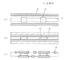
図1(a)〜(d)は本発明の第1の実施の形態における回路形成基板の製造方法および回路形成基板の製造用材料を示す工程断面図である。
(Embodiment 1)
1A to 1D are process cross-sectional views illustrating a method for manufacturing a circuit forming substrate and a material for manufacturing the circuit forming substrate according to the first embodiment of the present invention.
まず、金属箔としての処理銅箔1は、回路形成基板の製造用材料であって、厚み18μmの電解銅箔である。電解銅箔の製造時に硫酸銅水溶液中の陰極ドラム外側面は、電解作用で銅が電着・成長する際に凹凸が出来、Rz(10点平均粗さ)が約10μmの粗化面(マット面)となる。 First, the treated copper foil 1 as a metal foil is a material for manufacturing a circuit forming substrate, and is an electrolytic copper foil having a thickness of 18 μm. When manufacturing the electrolytic copper foil, the outer surface of the cathode drum in the aqueous copper sulfate solution is uneven when copper is electrodeposited and grown by electrolysis, and the roughened surface (mat) has an Rz (10-point average roughness) of about 10 μm. Surface).
また本発明の処理銅箔1は、マット面の反対側、すなわち陰極ドラム面(光沢面、シャイニィ面)側にも再度こぶ状の銅を析出させる粗化処理を施し、Rzで約5μmの凹凸を形成して圧力吸収手段1aを備えた構成である。 In addition, the treated copper foil 1 of the present invention is subjected to a roughening treatment for depositing a knot-like copper again on the opposite side of the mat surface, that is, on the cathode drum surface (glossy surface, shiny surface) side, and an unevenness of about 5 μm in Rz. And having a pressure absorbing means 1a.
次に、基板材料2は、プリプレグの両面にフィルムを張り付け、レーザ等の加工法により基板材料2にビア穴を形成し、導電性ペースト3を充填した後にフィルムを剥離することで層間接続手段を配設した構成である。 Next, the substrate material 2 is formed by attaching films on both sides of the prepreg, forming via holes in the substrate material 2 by a processing method such as a laser, filling the conductive paste 3, and then peeling the film to provide an interlayer connection means. It is the arrangement | positioning.
図1(a)に示すように、積層工程において基板材料2と処理銅箔1を重ねて配置し、次に図1(b)に示すように、SUS等の金属板4に挟み込んで積層物とし、それを熱プレス工程で加熱加圧して一体化する。
As shown in FIG. 1 (a), the substrate material 2 and the treated copper foil 1 are arranged in a stacking process in the laminating step, and then sandwiched between
図1(a)の状態で配置する際に、処理銅箔1のマット面(Rz:約10μm)は基板材料2に面する側になるよう配置することで、その反対側のシャイニィ面(Rz:約5μm)は圧力吸収手段1aとして機能する。この粗化構造を備えた構成により、基板材料2と処理銅箔1の熱プレス後の接着強度と後述する圧力の吸収作用を両立させる意味合いで有効である。また、処理銅箔1の表面粗さは、基板材料2に面する側(マット面)が、その反対面(シャイニィ面)より大であることが望ましい。 When arranging in the state shown in FIG. 1A, the matte surface (Rz: about 10 μm) of the treated copper foil 1 is disposed on the side facing the substrate material 2 so that the shiny surface (Rz) on the opposite side is arranged. : About 5 μm) functions as the pressure absorbing means 1a. This configuration with the roughened structure is effective in the sense that both the adhesive strength after hot pressing of the substrate material 2 and the treated copper foil 1 and the pressure absorbing action described below are compatible. Further, the surface roughness of the treated copper foil 1 is desirably such that the side facing the substrate material 2 (matte surface) is larger than the opposite surface (shiny surface).
加熱加圧時には図1(b)に示すように、処理銅箔1の外側の粗化部である圧力吸収手段1aがつぶされて圧力を吸収する。この作用が無いと導電性ペースト3に加圧力が集中し、従来例で述べたような課題が発生する。 At the time of heating and pressurizing, as shown in FIG. 1 (b), the pressure absorbing means 1 a that is a roughened portion outside the treated copper foil 1 is crushed and absorbs pressure. Without this action, the applied pressure concentrates on the conductive paste 3 and the problem described in the conventional example occurs.
処理銅箔1の圧力吸収手段1a(粗化部)がつぶれて、樹脂流動等により厚みの減少した基板材料2上の処理銅箔1の高さと導電性ペースト3上の処理銅箔1の高さがほぼ同一になった時点からは有効に導電性ペースト3に圧力が加わり、導電性ペースト3中の銅粒子と処理銅箔1の内側の粗化面が圧接され安定な電気的接続が得られる。 The height of the treated copper foil 1 on the substrate material 2 and the height of the treated copper foil 1 on the conductive paste 3 are reduced due to collapse of the pressure absorbing means 1a (roughening part) of the treated copper foil 1 due to resin flow or the like. Since the pressure is effectively applied to the conductive paste 3 from the time when the lengths are almost the same, the copper particles in the conductive paste 3 and the roughened surface on the inner side of the treated copper foil 1 are pressed to obtain a stable electrical connection. It is done.
次に、図1(c)に示すように処理銅箔1をエッチングして所望形状の回路5を形成して回路形成基板10を得る。
Next, as shown in FIG. 1C, the treated copper foil 1 is etched to form a
さらに、図1(d)に示すように回路5の表面の圧力吸収手段1a(粗化部)をバフ研磨あるいは軽度のエッチング等の手法を用いて光沢化、すなわち除去し、半田付け時の濡れ性を向上させる。
Further, as shown in FIG. 1 (d), the pressure absorbing means 1a (roughened portion) on the surface of the
ソルダーレジストを形成する際は、形成後に圧力吸収手段1aを除去する工程を経て光沢化しても良い。また、エッチングにより回路5を形成する前に光沢化を行うことも可能である。
When forming the solder resist, the solder resist may be glossed through a step of removing the pressure absorbing means 1a after the formation. It is also possible to gloss before forming the
ただし、図2に示したような多層回路形成基板を製造する過程において、コア回路形成基板として本実施の形態の回路形成基板10を使用する際は、図1(c)の状態、すなわち回路5が形成された処理銅箔1に圧力吸収手段1aが残存し表面が粗化されている状態のまま使用することが層間の接着強度を保つ面等から有効である。
However, when the
なお多層の回路形成基板の製造方法は、まず図2(a)に示すように、本実施の形態で製造した回路形成基板10をコア回路形成基板として準備する。
In the multilayer circuit formation substrate manufacturing method, first, as shown in FIG. 2A, the
次に、図2(b)〜(d)に示すように、コア回路形成基板10の上下に、導電性ペースト3が充填された層間接続手段を配設した基板材料2と、圧力吸収手段1aを備えた処理銅箔1を、位置合わせをしながら重ね合わせて積層物とし、それを熱プレス工程で一体化する。その後表層に回路5を形成することで、多層の回路形成基板を得ることが出来る(図2(e))。
Next, as shown in FIGS. 2B to 2D, the substrate material 2 in which the interlayer connection means filled with the conductive paste 3 is disposed above and below the core
(実施の形態2)
図3に示す回路形成基板の製造用材料は片面を粗化した処理銅箔1の光沢面(シャイニィ面)側に圧力吸収手段としての変形層6を形成したものである。
(Embodiment 2)
The material for manufacturing the circuit forming substrate shown in FIG. 3 is obtained by forming a deformable layer 6 as a pressure absorbing means on the glossy surface (shiny surface) side of the treated copper foil 1 having one surface roughened.
変形層6には有機材料、無機材料の種々の材質を用いることが可能であるが、熱プレス工程にて変形する材質、または処理銅箔に用いた銅材料より硬度が低いことがその機能からして望ましい。 Various materials such as an organic material and an inorganic material can be used for the deformable layer 6, but the material has a lower hardness than the material deformed in the hot press process or the copper material used for the treated copper foil. Is desirable.
発明者の検討では、耐熱性の良いエポキシ樹脂やシリコン樹脂の皮膜をキャスティングもしくはカーテンコート等の方法で、10μm程度の厚みに形成した変形層6を備えた処理銅箔1を準備し、それを実施の形態1で説明した回路形成基板の製造方法において使用した結果、同等の効果を確認している。 In the inventor's study, a treated copper foil 1 having a deformation layer 6 in which a heat-resistant epoxy resin or silicon resin film is formed to a thickness of about 10 μm by a method such as casting or curtain coating is prepared. As a result of using the circuit forming substrate manufacturing method described in the first embodiment, the same effect is confirmed.
また、本発明は上記したような導電性ペーストを用いた回路形成基板の製造において格別の効果をもたらすが、導電性ペーストを用いない回路形成基板の製造においても、層間接続手段としてめっき等を用いた際に、めっきを施した後に熱プレスを行い積層する際にめっきによる層間接続部が加圧によりダメージを受けることを回避できる等の効果がある。 In addition, the present invention brings about a special effect in the manufacture of a circuit forming substrate using the conductive paste as described above. However, in the manufacture of a circuit forming substrate using no conductive paste, plating or the like is used as an interlayer connection means. In this case, there is an effect such that it is possible to avoid damage caused by pressurization between the interlayer connection portions due to the plating when performing the heat press after the plating and laminating.
以上述べた実施の形態1から2で基板材料すなわちプリプレグとして説明した材料の例としては、通常のガラス繊維織布あるいは不織布に熱硬化性樹脂を含浸しBステージ化したものを用いることが可能でガラス繊維の代わりにアラミド等の有機繊維を採用することもできる。 As an example of the material described as the substrate material, that is, the prepreg in the first and second embodiments described above, it is possible to use a normal glass fiber woven fabric or non-woven fabric impregnated with a thermosetting resin to form a B stage. Organic fibers such as aramid can be used instead of glass fibers.
またプリプレグに代えてBステージフィルムもしくはポリイミド等の樹脂フィルムと接着剤からなるBステージ材料の使用も可能である。 Further, it is possible to use a B stage material made of a B stage film or a resin film such as polyimide and an adhesive instead of the prepreg.
また、織布と不織布を混成した材料、たとえば2枚のガラス繊維の間にガラス繊維不織布を挟み込んだような材料を補強剤として用いることも可能である。 Moreover, it is also possible to use the material which mixed the woven fabric and the nonwoven fabric, for example, the material which inserted | pinched the glass fiber nonwoven fabric between two glass fibers as a reinforcing agent.
また、本発明の実施の形態で基板材料もしくは熱硬化性樹脂と記述した部分の熱硬化性樹脂の例としては、エポキシ系樹脂、エポキシ・メラミン系樹脂、不飽和ポリエステル系樹脂、フェノール系樹脂ポリイミド系樹脂、シアネート系樹脂、シアン酸エステル系樹脂、ナフタレン系樹脂、ユリア系樹脂、アミノ系樹脂、アルキド系樹脂、ケイ素系樹脂、フラン系樹脂、ポリウレタン系樹脂、アミノアルキド系樹脂、アクリル系樹脂、フッ素系樹脂、ポリフェニレンエーテル系樹脂、シアネートエステル系樹脂等の単独、あるいは2種以上混合した熱硬化性樹脂組成物あるいは熱可塑性樹脂で変性された熱硬化性樹脂組成物を用いることができ、必要に応じて難燃剤や無機充填剤の添加も可能である。 In addition, examples of the thermosetting resin in the portion described as the substrate material or the thermosetting resin in the embodiment of the present invention include an epoxy resin, an epoxy / melamine resin, an unsaturated polyester resin, and a phenol resin polyimide. Resin, cyanate resin, cyanate ester resin, naphthalene resin, urea resin, amino resin, alkyd resin, silicon resin, furan resin, polyurethane resin, aminoalkyd resin, acrylic resin, Fluorine-based resin, polyphenylene ether-based resin, cyanate ester-based resin, etc. can be used alone, or two or more thermosetting resin compositions or thermosetting resin compositions modified with thermoplastic resins can be used. Depending on the case, flame retardants and inorganic fillers can be added.
また、多層回路形成基板を製造する際にも本発明の適用は、特に有効である。 The application of the present invention is also particularly effective when manufacturing a multilayer circuit forming substrate.
その際には多層回路形成基板の全ての層に本発明の内容を適用しなくても、例えば比較的層間接続手段にダメージの加わりやすい外層部、すなわち10層基板であれば10層目のみもしくは8層目と10層目に本発明の内容を適用することでも効果を得ることができる。 In that case, even if the contents of the present invention are not applied to all the layers of the multilayer circuit formation substrate, for example, the outer layer portion that is relatively susceptible to damage to the interlayer connection means, that is, only the 10th layer in the case of a 10-layer substrate, or The effect can also be obtained by applying the contents of the present invention to the eighth and tenth layers.
また、層間接続手段として導電性ペーストを用いて説明したが、導電性ペーストとしては銅粉等の導電性粒子を硬化剤を含む熱硬化性樹脂に混練したものの他に、導電性粒子と熱プレス時に基板材料中に排出されてしまうような適当な粘度の高分子材料、あるいは溶剤等を混練したものもしくは異方導電性接着剤等多種の組成が利用可能である。 In addition, although the conductive paste has been described as the interlayer connection means, the conductive paste is not limited to the conductive particles such as copper powder kneaded with the thermosetting resin containing the curing agent, and the conductive particles and the hot press. Various compositions such as a polymer material having an appropriate viscosity that is sometimes discharged into the substrate material, a kneaded solvent, or an anisotropic conductive adhesive can be used.
さらに、導電性ペースト以外にめっき等により形成したポスト状の導電性突起や、ペースト化していない比較的大きな粒径の導電性粒子を単独で層間接続手段として用いることも可能である。 In addition to the conductive paste, post-shaped conductive protrusions formed by plating or the like, or conductive particles having a relatively large particle size that are not made into a paste can be used alone as an interlayer connection means.
以上述べたように、本発明の構成によれば導電性ペースト等の層間接続手段に対してダメージを与えること無く熱プレス等の積層工程を実施出来、導電性ペースト等の層間接続手段を用いた層間の電気的接続の品質信頼性が大幅に向上し、高品質の高密度回路形成基板を提供できるものであり、産業上の利用可能性は大といえる。 As described above, according to the configuration of the present invention, the laminating process such as hot pressing can be performed without damaging the interlayer connection means such as the conductive paste, and the interlayer connection means such as the conductive paste is used. The reliability of the quality of the electrical connection between the layers is greatly improved, and a high-quality high-density circuit-formed substrate can be provided. Thus, the industrial applicability is great.
1 処理銅箔
1a 圧力吸収手段
2 基板材料
3 導電性ペースト
4 金属板
5 回路
6 変形層
10 回路形成基板
DESCRIPTION OF SYMBOLS 1 Processed copper foil 1a Pressure absorption means 2 Substrate material 3
Claims (7)
前記圧力吸収手段は、基板材料に面する側の反対側の金属箔の表面に形成されている粗化構造のものであることを特徴とする回路形成基板の製造方法。 A lamination process in which a substrate material and a metal foil provided with interlayer connection means and a substrate material provided with an interlayer connection means, a core circuit forming substrate, and a metal foil provided with pressure absorption means are laminated to form a laminate; And a hot press process for integrating objects,
The method for producing a circuit-formed substrate, wherein the pressure absorbing means is of a roughened structure formed on the surface of the metal foil opposite to the side facing the substrate material.
前記回路形成基板の上下に層間接続手段を配設した基板材料と金属箔とを重ね合わせて積層物を形成する工程と、
前記積層物を一体化する熱プレス工程とを備えたことを特徴とする回路形成基板の製造方法。 Preparing a circuit forming substrate manufactured using the method for manufacturing a circuit forming substrate according to claim 1 and having a circuit;
Forming a laminate by superimposing a substrate material and metal foil on which interlayer connection means are disposed above and below the circuit forming substrate; and
A circuit forming substrate manufacturing method comprising: a hot pressing step of integrating the laminate.
前記圧力吸収手段は、基板材料に面する側の反対側の金属箔の表面に形成されている粗化構造のものであることを特徴とする回路形成基板の製造用材料。 A material mainly composed of a metal foil used for a circuit forming substrate configured by laminating a substrate material and a metal foil and integrated in a hot press process, and the metal foil includes pressure absorbing means,
The material for manufacturing a circuit forming substrate, wherein the pressure absorbing means has a roughened structure formed on the surface of the metal foil opposite to the side facing the substrate material.
Priority Applications (8)
| Application Number | Priority Date | Filing Date | Title |
|---|---|---|---|
| JP2004016795A JP3979391B2 (en) | 2004-01-26 | 2004-01-26 | Circuit forming substrate manufacturing method and circuit forming substrate manufacturing material |
| TW094101542A TW200527995A (en) | 2004-01-26 | 2005-01-19 | Method for producing circuit-forming board and material for producing circuit-forming board |
| PCT/JP2005/000763 WO2005072037A1 (en) | 2004-01-26 | 2005-01-21 | Method for producing circuit-forming board and material for producing circuit-forming board |
| EP05703984A EP1599079B1 (en) | 2004-01-26 | 2005-01-21 | Method for producing a circuit board and material for producing a circuit board |
| CNB2005800002557A CN100539813C (en) | 2004-01-26 | 2005-01-21 | Circuit-forming board manufacture method and the material that is used to make circuit-forming board |
| US10/546,730 US7624502B2 (en) | 2004-01-26 | 2005-01-21 | Method for producing circuit-forming board and material for producing circuit-forming board |
| KR1020057017222A KR100736518B1 (en) | 2004-01-26 | 2005-01-21 | Method for producing circuit-forming board and material for producing circuit-forming board |
| US11/882,396 US7572500B2 (en) | 2004-01-26 | 2007-08-01 | Method of manufacturing circuit-forming board and material of circuit-forming board |
Applications Claiming Priority (1)
| Application Number | Priority Date | Filing Date | Title |
|---|---|---|---|
| JP2004016795A JP3979391B2 (en) | 2004-01-26 | 2004-01-26 | Circuit forming substrate manufacturing method and circuit forming substrate manufacturing material |
Publications (2)
| Publication Number | Publication Date |
|---|---|
| JP2005209993A JP2005209993A (en) | 2005-08-04 |
| JP3979391B2 true JP3979391B2 (en) | 2007-09-19 |
Family
ID=34805507
Family Applications (1)
| Application Number | Title | Priority Date | Filing Date |
|---|---|---|---|
| JP2004016795A Expired - Fee Related JP3979391B2 (en) | 2004-01-26 | 2004-01-26 | Circuit forming substrate manufacturing method and circuit forming substrate manufacturing material |
Country Status (7)
| Country | Link |
|---|---|
| US (2) | US7624502B2 (en) |
| EP (1) | EP1599079B1 (en) |
| JP (1) | JP3979391B2 (en) |
| KR (1) | KR100736518B1 (en) |
| CN (1) | CN100539813C (en) |
| TW (1) | TW200527995A (en) |
| WO (1) | WO2005072037A1 (en) |
Families Citing this family (12)
| Publication number | Priority date | Publication date | Assignee | Title |
|---|---|---|---|---|
| JP4903723B2 (en) * | 2006-01-30 | 2012-03-28 | 京セラ株式会社 | Wiring board and electronic device |
| KR100905566B1 (en) * | 2007-04-30 | 2009-07-02 | 삼성전기주식회사 | Carrier member for transmitting circuits, coreless printed circuit board using the said carrier member, and methods of manufacturing the same |
| CN101562952B (en) * | 2008-04-18 | 2012-04-11 | 富葵精密组件(深圳)有限公司 | Circuit substrate, manufacture method of circuit substrate and manufacture method of circuit wafer |
| KR100999918B1 (en) * | 2008-09-08 | 2010-12-13 | 삼성전기주식회사 | Printed circuit board and method of manufacturing the same |
| KR100982791B1 (en) * | 2010-07-08 | 2010-09-16 | 윤병철 | Method for applying an electric connect from the upper side to the lower side of the insulator in non-pcb composite plate in use of metallic staple |
| KR100982790B1 (en) * | 2010-07-08 | 2010-09-16 | 윤병철 | Method for applying an electric connect from the upper side to the lower side of the insulator in non-pcb composite plate in use of metallic fiber |
| GB2489508B8 (en) | 2011-03-31 | 2016-03-16 | Plasyl Ltd | Improvements for electrical circuits |
| TW201340807A (en) * | 2011-12-28 | 2013-10-01 | Panasonic Corp | Flexible wiring board, method for manufacturing flexible wiring board, package product using flexible wiring board, and flexible multilayer wiring board |
| KR101494090B1 (en) * | 2013-07-16 | 2015-02-16 | 삼성전기주식회사 | Copper clad laminate, printed circuit board and method for manufacturing of the same |
| CN104768326B (en) * | 2015-03-31 | 2017-11-24 | 华为技术有限公司 | Printed circuit board (PCB) and board, printed circuit board manufacturing method |
| DE102018125919A1 (en) | 2017-10-23 | 2019-04-25 | Engel Austria Gmbh | Method for moving a movable platen |
| CN115837792B (en) * | 2022-12-12 | 2023-07-11 | 广东嘉元科技股份有限公司 | Automatic copper foil bonding device |
Family Cites Families (30)
| Publication number | Priority date | Publication date | Assignee | Title |
|---|---|---|---|---|
| DE3786600T2 (en) * | 1986-05-30 | 1993-11-04 | Furukawa Electric Co Ltd | MULTILAYER PRINTED CIRCUIT AND METHOD FOR THEIR PRODUCTION. |
| JPH07115280B2 (en) * | 1986-10-21 | 1995-12-13 | 日立精機株式会社 | Unbalanced tool measuring device |
| US5413838A (en) * | 1991-06-18 | 1995-05-09 | Sumitomo Bakelite Company Limited | Both-side roughened copper foil with protection film |
| US5344893A (en) * | 1991-07-23 | 1994-09-06 | Ibiden Co., Ltd. | Epoxy/amino powder resin adhesive for printed circuit board |
| JP2601128B2 (en) | 1992-05-06 | 1997-04-16 | 松下電器産業株式会社 | Method of manufacturing circuit forming substrate and circuit forming substrate |
| US5403672A (en) * | 1992-08-17 | 1995-04-04 | Hitachi Chemical Co., Ltd. | Metal foil for printed wiring board and production thereof |
| JP3146712B2 (en) * | 1993-01-12 | 2001-03-19 | 松下電器産業株式会社 | Double-sided printed circuit board and method of manufacturing the same |
| US5779870A (en) * | 1993-03-05 | 1998-07-14 | Polyclad Laminates, Inc. | Method of manufacturing laminates and printed circuit boards |
| US5519177A (en) * | 1993-05-19 | 1996-05-21 | Ibiden Co., Ltd. | Adhesives, adhesive layers for electroless plating and printed circuit boards |
| JP3173249B2 (en) * | 1993-10-20 | 2001-06-04 | 松下電器産業株式会社 | Multilayer printed wiring board and method of manufacturing the same |
| EP0651602B1 (en) * | 1993-10-29 | 1999-04-07 | Matsushita Electric Industrial Co., Ltd. | Conductive paste compound for via hole filling, printed circuit board which uses the conductive paste, and method of manufacturing the same |
| US5482784A (en) * | 1993-12-24 | 1996-01-09 | Mitsui Mining And Smelting Co., Ltd. | Printed circuit inner-layer copper foil and process for producing the same |
| JP3311899B2 (en) * | 1995-01-20 | 2002-08-05 | 松下電器産業株式会社 | Circuit board and method of manufacturing the same |
| JPH0946041A (en) * | 1995-07-26 | 1997-02-14 | Toshiba Corp | Manufacture of printed wiring board |
| US6010768A (en) * | 1995-11-10 | 2000-01-04 | Ibiden Co., Ltd. | Multilayer printed circuit board, method of producing multilayer printed circuit board and resin filler |
| US6085414A (en) * | 1996-08-15 | 2000-07-11 | Packard Hughes Interconnect Company | Method of making a flexible circuit with raised features protruding from two surfaces and products therefrom |
| KR100448561B1 (en) * | 1997-04-15 | 2004-09-13 | 이비덴 가부시키가이샤 | Adhesive for electroless plating, raw material composition for preparing adhesive for electroless plating and printed wiring board |
| US6239777B1 (en) * | 1997-07-22 | 2001-05-29 | Kabushiki Kaisha Toshiba | Display device |
| JPH11251703A (en) | 1998-02-27 | 1999-09-17 | Matsushita Electric Ind Co Ltd | Circuit board, both-sided circuit board, multilayered circuit board, and manufacture of circuit board |
| US6139777A (en) * | 1998-05-08 | 2000-10-31 | Matsushita Electric Industrial Co., Ltd. | Conductive paste for filling via-hole, double-sided and multilayer printed circuit boards using the same, and method for producing the same |
| JP4486196B2 (en) * | 1999-12-08 | 2010-06-23 | イビデン株式会社 | Single-sided circuit board for multilayer printed wiring board and manufacturing method thereof |
| US6504705B2 (en) * | 2000-10-12 | 2003-01-07 | Matsushita Electric Industrial Co., Ltd. | Electrolytic capacitor, circuit board containing electrolytic capacitor, and method for producing the same |
| US6713688B2 (en) * | 2000-12-27 | 2004-03-30 | Matsushita Electric Industrial Co., Ltd. | Circuit board and its manufacture method |
| JP2002217510A (en) * | 2001-01-15 | 2002-08-02 | Matsushita Electric Ind Co Ltd | Connecting structure of board, and its manufacturing method |
| JP2002368043A (en) * | 2001-06-12 | 2002-12-20 | Matsushita Electric Ind Co Ltd | Conductive paste, conductive bump using it, its forming method, method for connecting conductive bump, circuit board and its producing method |
| JP2003023250A (en) * | 2001-07-06 | 2003-01-24 | Denso Corp | Multilayered substrate and its manufacturing method |
| JP4062907B2 (en) * | 2001-11-12 | 2008-03-19 | 松下電器産業株式会社 | Circuit board and manufacturing method thereof |
| JP2003209355A (en) * | 2002-01-15 | 2003-07-25 | Sony Corp | Circuit board and method for manufacturing the same |
| US6946205B2 (en) * | 2002-04-25 | 2005-09-20 | Matsushita Electric Industrial Co., Ltd. | Wiring transfer sheet and method for producing the same, and wiring board and method for producing the same |
| JP4029759B2 (en) * | 2003-04-04 | 2008-01-09 | 株式会社デンソー | Multilayer circuit board and manufacturing method thereof |
-
2004
- 2004-01-26 JP JP2004016795A patent/JP3979391B2/en not_active Expired - Fee Related
-
2005
- 2005-01-19 TW TW094101542A patent/TW200527995A/en not_active IP Right Cessation
- 2005-01-21 EP EP05703984A patent/EP1599079B1/en not_active Expired - Fee Related
- 2005-01-21 US US10/546,730 patent/US7624502B2/en not_active Expired - Fee Related
- 2005-01-21 KR KR1020057017222A patent/KR100736518B1/en not_active IP Right Cessation
- 2005-01-21 CN CNB2005800002557A patent/CN100539813C/en not_active Expired - Fee Related
- 2005-01-21 WO PCT/JP2005/000763 patent/WO2005072037A1/en active Application Filing
-
2007
- 2007-08-01 US US11/882,396 patent/US7572500B2/en not_active Expired - Fee Related
Also Published As
| Publication number | Publication date |
|---|---|
| TW200527995A (en) | 2005-08-16 |
| CN100539813C (en) | 2009-09-09 |
| US7624502B2 (en) | 2009-12-01 |
| CN1771773A (en) | 2006-05-10 |
| KR100736518B1 (en) | 2007-07-06 |
| US7572500B2 (en) | 2009-08-11 |
| US20080017403A1 (en) | 2008-01-24 |
| JP2005209993A (en) | 2005-08-04 |
| KR20050110001A (en) | 2005-11-22 |
| EP1599079A4 (en) | 2008-05-21 |
| EP1599079A1 (en) | 2005-11-23 |
| TWI350718B (en) | 2011-10-11 |
| EP1599079B1 (en) | 2012-05-09 |
| WO2005072037A1 (en) | 2005-08-04 |
| US20060242827A1 (en) | 2006-11-02 |
Similar Documents
| Publication | Publication Date | Title |
|---|---|---|
| US7624502B2 (en) | Method for producing circuit-forming board and material for producing circuit-forming board | |
| WO2001045478A1 (en) | Multilayered printed wiring board and production method therefor | |
| JP4075673B2 (en) | Copper-clad laminate for multilayer printed wiring board, multilayer printed wiring board, and method for manufacturing multilayer printed wiring board | |
| TW511441B (en) | Multi-layer circuit board and method of manufacturing same | |
| JP2012015562A (en) | Method of manufacturing circuit board | |
| TWI241876B (en) | Circuit forming substrate, method of manufacturing the substrate, and material of the substrate | |
| JP3760771B2 (en) | Circuit forming substrate and method of manufacturing circuit forming substrate | |
| TW558931B (en) | Manufacturing method of printed wiring boards and material for manufacturing printed wiring boards | |
| JP2006313932A (en) | Multilayer circuit board and manufacturing method therefor | |
| JP3587457B2 (en) | Circuit board and its manufacturing method | |
| JPWO2003009656A1 (en) | Circuit forming substrate manufacturing method and circuit forming substrate | |
| JP2006306977A (en) | Composite, prepreg, metal foil-clad laminated board, printed-wiring board, multilayer printed-wiring board and manufacturing method thereof | |
| JP4436714B2 (en) | Manufacturing method of rigid flexible metal-clad laminate and manufacturing method of rigid flexible printed wiring board | |
| JP2006160899A (en) | Manufacturing methods of electrically insulating substrate and wiring board | |
| JP2006348225A (en) | Composite, prepreg, metallic foil clad laminate and printed wiring substrate using the same, and method for manufacturing printed wiring substrate | |
| JP4089671B2 (en) | Circuit forming substrate manufacturing method and circuit forming substrate | |
| JP3985764B2 (en) | Circuit forming substrate manufacturing material and circuit forming substrate manufacturing method | |
| JP5196056B1 (en) | Composite multilayer wiring board and manufacturing method thereof | |
| JP5045664B2 (en) | Method for manufacturing circuit-formed substrate | |
| JP4774606B2 (en) | Method for manufacturing circuit-formed substrate | |
| JP2011082429A (en) | Multilayer wiring board having cavity portion and method of manufacturing the same | |
| JP5050656B2 (en) | Method for manufacturing circuit-formed substrate | |
| JP2007165436A (en) | Process for manufacturing circuit board | |
| JP2006086544A (en) | Circuit forming substrate and method of manufacturing the circuit forming substrate | |
| JP4407456B2 (en) | Method for manufacturing circuit-forming substrate manufacturing material and circuit-forming substrate manufacturing material |
Legal Events
| Date | Code | Title | Description |
|---|---|---|---|
| A621 | Written request for application examination |
Free format text: JAPANESE INTERMEDIATE CODE: A621 Effective date: 20050620 |
|
| RD01 | Notification of change of attorney |
Free format text: JAPANESE INTERMEDIATE CODE: A7421 Effective date: 20050713 |
|
| A131 | Notification of reasons for refusal |
Free format text: JAPANESE INTERMEDIATE CODE: A131 Effective date: 20070327 |
|
| A521 | Request for written amendment filed |
Free format text: JAPANESE INTERMEDIATE CODE: A523 Effective date: 20070510 |
|
| TRDD | Decision of grant or rejection written | ||
| A01 | Written decision to grant a patent or to grant a registration (utility model) |
Free format text: JAPANESE INTERMEDIATE CODE: A01 Effective date: 20070605 |
|
| A61 | First payment of annual fees (during grant procedure) |
Free format text: JAPANESE INTERMEDIATE CODE: A61 Effective date: 20070618 |
|
| FPAY | Renewal fee payment (event date is renewal date of database) |
Free format text: PAYMENT UNTIL: 20100706 Year of fee payment: 3 |
|
| FPAY | Renewal fee payment (event date is renewal date of database) |
Free format text: PAYMENT UNTIL: 20110706 Year of fee payment: 4 |
|
| FPAY | Renewal fee payment (event date is renewal date of database) |
Free format text: PAYMENT UNTIL: 20110706 Year of fee payment: 4 |
|
| FPAY | Renewal fee payment (event date is renewal date of database) |
Free format text: PAYMENT UNTIL: 20120706 Year of fee payment: 5 |
|
| FPAY | Renewal fee payment (event date is renewal date of database) |
Free format text: PAYMENT UNTIL: 20120706 Year of fee payment: 5 |
|
| FPAY | Renewal fee payment (event date is renewal date of database) |
Free format text: PAYMENT UNTIL: 20130706 Year of fee payment: 6 |
|
| LAPS | Cancellation because of no payment of annual fees |