EP1599079A1 - Method for producing circuit-forming board and material for producing circuit-forming board - Google Patents
Method for producing circuit-forming board and material for producing circuit-forming board Download PDFInfo
- Publication number
- EP1599079A1 EP1599079A1 EP05703984A EP05703984A EP1599079A1 EP 1599079 A1 EP1599079 A1 EP 1599079A1 EP 05703984 A EP05703984 A EP 05703984A EP 05703984 A EP05703984 A EP 05703984A EP 1599079 A1 EP1599079 A1 EP 1599079A1
- Authority
- EP
- European Patent Office
- Prior art keywords
- metal foil
- pressure absorption
- board
- circuit
- absorption portion
- Prior art date
- Legal status (The legal status is an assumption and is not a legal conclusion. Google has not performed a legal analysis and makes no representation as to the accuracy of the status listed.)
- Granted
Links
Images


Classifications
-
- H—ELECTRICITY
- H05—ELECTRIC TECHNIQUES NOT OTHERWISE PROVIDED FOR
- H05K—PRINTED CIRCUITS; CASINGS OR CONSTRUCTIONAL DETAILS OF ELECTRIC APPARATUS; MANUFACTURE OF ASSEMBLAGES OF ELECTRICAL COMPONENTS
- H05K3/00—Apparatus or processes for manufacturing printed circuits
- H05K3/40—Forming printed elements for providing electric connections to or between printed circuits
- H05K3/4038—Through-connections; Vertical interconnect access [VIA] connections
- H05K3/4053—Through-connections; Vertical interconnect access [VIA] connections by thick-film techniques
- H05K3/4069—Through-connections; Vertical interconnect access [VIA] connections by thick-film techniques for via connections in organic insulating substrates
-
- H—ELECTRICITY
- H05—ELECTRIC TECHNIQUES NOT OTHERWISE PROVIDED FOR
- H05K—PRINTED CIRCUITS; CASINGS OR CONSTRUCTIONAL DETAILS OF ELECTRIC APPARATUS; MANUFACTURE OF ASSEMBLAGES OF ELECTRICAL COMPONENTS
- H05K3/00—Apparatus or processes for manufacturing printed circuits
- H05K3/46—Manufacturing multilayer circuits
-
- H—ELECTRICITY
- H05—ELECTRIC TECHNIQUES NOT OTHERWISE PROVIDED FOR
- H05K—PRINTED CIRCUITS; CASINGS OR CONSTRUCTIONAL DETAILS OF ELECTRIC APPARATUS; MANUFACTURE OF ASSEMBLAGES OF ELECTRICAL COMPONENTS
- H05K3/00—Apparatus or processes for manufacturing printed circuits
- H05K3/40—Forming printed elements for providing electric connections to or between printed circuits
-
- H—ELECTRICITY
- H05—ELECTRIC TECHNIQUES NOT OTHERWISE PROVIDED FOR
- H05K—PRINTED CIRCUITS; CASINGS OR CONSTRUCTIONAL DETAILS OF ELECTRIC APPARATUS; MANUFACTURE OF ASSEMBLAGES OF ELECTRICAL COMPONENTS
- H05K2201/00—Indexing scheme relating to printed circuits covered by H05K1/00
- H05K2201/03—Conductive materials
- H05K2201/0332—Structure of the conductor
- H05K2201/0335—Layered conductors or foils
- H05K2201/0355—Metal foils
-
- H—ELECTRICITY
- H05—ELECTRIC TECHNIQUES NOT OTHERWISE PROVIDED FOR
- H05K—PRINTED CIRCUITS; CASINGS OR CONSTRUCTIONAL DETAILS OF ELECTRIC APPARATUS; MANUFACTURE OF ASSEMBLAGES OF ELECTRICAL COMPONENTS
- H05K2201/00—Indexing scheme relating to printed circuits covered by H05K1/00
- H05K2201/03—Conductive materials
- H05K2201/0332—Structure of the conductor
- H05K2201/0335—Layered conductors or foils
- H05K2201/0358—Resin coated copper [RCC]
-
- H—ELECTRICITY
- H05—ELECTRIC TECHNIQUES NOT OTHERWISE PROVIDED FOR
- H05K—PRINTED CIRCUITS; CASINGS OR CONSTRUCTIONAL DETAILS OF ELECTRIC APPARATUS; MANUFACTURE OF ASSEMBLAGES OF ELECTRICAL COMPONENTS
- H05K2201/00—Indexing scheme relating to printed circuits covered by H05K1/00
- H05K2201/03—Conductive materials
- H05K2201/0332—Structure of the conductor
- H05K2201/0364—Conductor shape
- H05K2201/0382—Continuously deformed conductors
-
- H—ELECTRICITY
- H05—ELECTRIC TECHNIQUES NOT OTHERWISE PROVIDED FOR
- H05K—PRINTED CIRCUITS; CASINGS OR CONSTRUCTIONAL DETAILS OF ELECTRIC APPARATUS; MANUFACTURE OF ASSEMBLAGES OF ELECTRICAL COMPONENTS
- H05K2201/00—Indexing scheme relating to printed circuits covered by H05K1/00
- H05K2201/09—Shape and layout
- H05K2201/09009—Substrate related
- H05K2201/091—Locally and permanently deformed areas including dielectric material
-
- H—ELECTRICITY
- H05—ELECTRIC TECHNIQUES NOT OTHERWISE PROVIDED FOR
- H05K—PRINTED CIRCUITS; CASINGS OR CONSTRUCTIONAL DETAILS OF ELECTRIC APPARATUS; MANUFACTURE OF ASSEMBLAGES OF ELECTRICAL COMPONENTS
- H05K2203/00—Indexing scheme relating to apparatus or processes for manufacturing printed circuits covered by H05K3/00
- H05K2203/14—Related to the order of processing steps
- H05K2203/1461—Applying or finishing the circuit pattern after another process, e.g. after filling of vias with conductive paste, after making printed resistors
-
- H—ELECTRICITY
- H05—ELECTRIC TECHNIQUES NOT OTHERWISE PROVIDED FOR
- H05K—PRINTED CIRCUITS; CASINGS OR CONSTRUCTIONAL DETAILS OF ELECTRIC APPARATUS; MANUFACTURE OF ASSEMBLAGES OF ELECTRICAL COMPONENTS
- H05K3/00—Apparatus or processes for manufacturing printed circuits
- H05K3/38—Improvement of the adhesion between the insulating substrate and the metal
- H05K3/382—Improvement of the adhesion between the insulating substrate and the metal by special treatment of the metal
-
- H—ELECTRICITY
- H05—ELECTRIC TECHNIQUES NOT OTHERWISE PROVIDED FOR
- H05K—PRINTED CIRCUITS; CASINGS OR CONSTRUCTIONAL DETAILS OF ELECTRIC APPARATUS; MANUFACTURE OF ASSEMBLAGES OF ELECTRICAL COMPONENTS
- H05K3/00—Apparatus or processes for manufacturing printed circuits
- H05K3/46—Manufacturing multilayer circuits
- H05K3/4611—Manufacturing multilayer circuits by laminating two or more circuit boards
- H05K3/4614—Manufacturing multilayer circuits by laminating two or more circuit boards the electrical connections between the circuit boards being made during lamination
-
- H—ELECTRICITY
- H05—ELECTRIC TECHNIQUES NOT OTHERWISE PROVIDED FOR
- H05K—PRINTED CIRCUITS; CASINGS OR CONSTRUCTIONAL DETAILS OF ELECTRIC APPARATUS; MANUFACTURE OF ASSEMBLAGES OF ELECTRICAL COMPONENTS
- H05K3/00—Apparatus or processes for manufacturing printed circuits
- H05K3/46—Manufacturing multilayer circuits
- H05K3/4644—Manufacturing multilayer circuits by building the multilayer layer by layer, i.e. build-up multilayer circuits
- H05K3/4652—Adding a circuit layer by laminating a metal foil or a preformed metal foil pattern
-
- Y—GENERAL TAGGING OF NEW TECHNOLOGICAL DEVELOPMENTS; GENERAL TAGGING OF CROSS-SECTIONAL TECHNOLOGIES SPANNING OVER SEVERAL SECTIONS OF THE IPC; TECHNICAL SUBJECTS COVERED BY FORMER USPC CROSS-REFERENCE ART COLLECTIONS [XRACs] AND DIGESTS
- Y10—TECHNICAL SUBJECTS COVERED BY FORMER USPC
- Y10T—TECHNICAL SUBJECTS COVERED BY FORMER US CLASSIFICATION
- Y10T29/00—Metal working
- Y10T29/49—Method of mechanical manufacture
- Y10T29/49002—Electrical device making
- Y10T29/49117—Conductor or circuit manufacturing
- Y10T29/49124—On flat or curved insulated base, e.g., printed circuit, etc.
- Y10T29/49126—Assembling bases
-
- Y—GENERAL TAGGING OF NEW TECHNOLOGICAL DEVELOPMENTS; GENERAL TAGGING OF CROSS-SECTIONAL TECHNOLOGIES SPANNING OVER SEVERAL SECTIONS OF THE IPC; TECHNICAL SUBJECTS COVERED BY FORMER USPC CROSS-REFERENCE ART COLLECTIONS [XRACs] AND DIGESTS
- Y10—TECHNICAL SUBJECTS COVERED BY FORMER USPC
- Y10T—TECHNICAL SUBJECTS COVERED BY FORMER US CLASSIFICATION
- Y10T29/00—Metal working
- Y10T29/49—Method of mechanical manufacture
- Y10T29/49002—Electrical device making
- Y10T29/49117—Conductor or circuit manufacturing
- Y10T29/49124—On flat or curved insulated base, e.g., printed circuit, etc.
- Y10T29/49128—Assembling formed circuit to base
-
- Y—GENERAL TAGGING OF NEW TECHNOLOGICAL DEVELOPMENTS; GENERAL TAGGING OF CROSS-SECTIONAL TECHNOLOGIES SPANNING OVER SEVERAL SECTIONS OF THE IPC; TECHNICAL SUBJECTS COVERED BY FORMER USPC CROSS-REFERENCE ART COLLECTIONS [XRACs] AND DIGESTS
- Y10—TECHNICAL SUBJECTS COVERED BY FORMER USPC
- Y10T—TECHNICAL SUBJECTS COVERED BY FORMER US CLASSIFICATION
- Y10T29/00—Metal working
- Y10T29/49—Method of mechanical manufacture
- Y10T29/49002—Electrical device making
- Y10T29/49117—Conductor or circuit manufacturing
- Y10T29/49124—On flat or curved insulated base, e.g., printed circuit, etc.
- Y10T29/4913—Assembling to base an electrical component, e.g., capacitor, etc.
- Y10T29/49139—Assembling to base an electrical component, e.g., capacitor, etc. by inserting component lead or terminal into base aperture
-
- Y—GENERAL TAGGING OF NEW TECHNOLOGICAL DEVELOPMENTS; GENERAL TAGGING OF CROSS-SECTIONAL TECHNOLOGIES SPANNING OVER SEVERAL SECTIONS OF THE IPC; TECHNICAL SUBJECTS COVERED BY FORMER USPC CROSS-REFERENCE ART COLLECTIONS [XRACs] AND DIGESTS
- Y10—TECHNICAL SUBJECTS COVERED BY FORMER USPC
- Y10T—TECHNICAL SUBJECTS COVERED BY FORMER US CLASSIFICATION
- Y10T29/00—Metal working
- Y10T29/49—Method of mechanical manufacture
- Y10T29/49002—Electrical device making
- Y10T29/49117—Conductor or circuit manufacturing
- Y10T29/49124—On flat or curved insulated base, e.g., printed circuit, etc.
- Y10T29/49155—Manufacturing circuit on or in base
- Y10T29/49165—Manufacturing circuit on or in base by forming conductive walled aperture in base
-
- Y—GENERAL TAGGING OF NEW TECHNOLOGICAL DEVELOPMENTS; GENERAL TAGGING OF CROSS-SECTIONAL TECHNOLOGIES SPANNING OVER SEVERAL SECTIONS OF THE IPC; TECHNICAL SUBJECTS COVERED BY FORMER USPC CROSS-REFERENCE ART COLLECTIONS [XRACs] AND DIGESTS
- Y10—TECHNICAL SUBJECTS COVERED BY FORMER USPC
- Y10T—TECHNICAL SUBJECTS COVERED BY FORMER US CLASSIFICATION
- Y10T428/00—Stock material or miscellaneous articles
- Y10T428/24—Structurally defined web or sheet [e.g., overall dimension, etc.]
- Y10T428/24802—Discontinuous or differential coating, impregnation or bond [e.g., artwork, printing, retouched photograph, etc.]
- Y10T428/24917—Discontinuous or differential coating, impregnation or bond [e.g., artwork, printing, retouched photograph, etc.] including metal layer
Definitions
- the present invention relates to a method of manufacturing a circuit-forming board for providing a circuit board used in various electronic equipment, and to a material for manufacturing the circuit-forming board.
- circuit boards having electronic components mounted thereon shift from single-sided circuit boards to double-sided, multi-layer circuit boards.
- High-density circuit boards capable of integrating an increasing number of circuits and components have accordingly developed.
- Figs. 5A to 5G are sectional views of a conventional circuit-forming board providing a circuit board for illustrating a method of manufacturing the board disclosed in Japanese Patent Laid-Open Publication No.6-268345.
- films 17 are attached onto both surfaces of pre-preg sheet 12 by a laminating method using, e.g. a thermal roll.
- Pre-preg sheet 12 is obtained by drying woven fabric of glass fiber (reinforcing material) impregnated with varnish of thermosetting resin, such as epoxy resin.
- Pre-preg sheet 12 is in a B-stage and has a thickness of 100 ⁇ m.
- Film 17 is made of polyethylene terephthalate (PET) having a thickness of 20 ⁇ m. Film 17 may be coated with thermosetting resin, such as epoxy resin.
- via-holes 18 are formed in pre-preg sheet 12 by a process, such as a laser technology.
- via-holes 18 are filled with conductive pastes 13 obtained by kneading thermosetting resin, hardening agent, solvent, and conductive particles, such as copper powder,
- films 17 are peeled off.
- Conductive pastes 13 protrude from pre-preg sheet 12.
- copper foils 19 are placed on both surfaces of pre-preg sheet 12.
- pre-preg sheet 12 is pressed by a hot-pressing apparatus (not shown) so as to heat pre-preg sheet 12, copper foils 19, and conductive pastes 13.
- This operation hardens pre-preg sheet 12 thermally, and compresses conductive pastes 13 as to allow conductive pastes 13 to be electrically connected to copper foils 19, as shown in Fig. 5E.
- the resin impregnated in pre-preg sheet 12 flows to outsides of pre-preg sheet 12, providing resin 12A.
- circuit-forming board an unnecessary portion at an end is cut off, thus providing the circuit-forming board.
- copper foils 19 are etched to have predetermined circuit patterns to provide circuit patterns 15 shown in Fig. 5G, thereby providing a double-sided circuit board.
- This board is cut to provide circuit board 16 having a predetermined size.
- a solder resist may be formed on circuit pattern 15 in order to prevent the pattern from having an unnecessary solder attached thereto.
- Circuit patterns 15 may be subjected to a finishing process, such as plating process.
- Figs. 6A to 6E are sectional views of a multi-layer circuit board obtained with using circuit board 16 manufactured by the method shown in Figs. 5A to 5G for illustrating a method of manufacturing the multi-layer circuit board.
- Pre-preg sheets 12B filled with conductive pastes 13A and copper foils 19A are positioned and placed on both surfaces of circuit board 16 as a core, and are heated and pressed as to provide multi-layer circuit board 20 having circuit patterns 15A on both surfaces thereof.
- conductive pastes 13 and 13A heated and pressed by, e.g. a hot-press apparatus may cause the following problem.
- Figs. 7A to 7C are sectional views of the circuit-forming board shown in Figs. 5A to 5G.
- copper foils 19 are placed on both surfaces of pre-preg sheet 12 having via-holes 18 filled with conductive pastes 13. These are sandwiched between metal plates 14, heated, and pressing, being compressed. A pressure applied to them may cause conductive pastes 13 to deform, distorting the shapes of pastes 13, as shown in Fig. 7B
- circuit patterns 15 are formed, and conductive pastes 13 become interlayer-connecting portions 13D and 13C adjacent to each other. If the circuit board has a high density, the distance for insulation between interlayer connecting portions 13D and 13C is reduced due to the deformation of conductive pastes 13, thereby reducing electrical insulation between the pastes.
- pre-preg sheet 12 When pre-preg sheet 12 is heated and pressed, the resin impregnated into pre-preg sheet 12 flows. When an excessive pressure is applied to conductive paste 13, conductive pastes 13 spread in in-plane direction 12D more than in thickness direction 12C. Thereby, the conductive particles in conductive pastes 13 are not pressed strongly and do not contact each other, so that sufficient electrical connection cannot be obtained. This phenomenon appears significantly if the diameter of each via-hole 18 is smaller than the thickness of pre-preg sheet 12.
- circuit board 16 as the core has a rough surface provided by circuit patterns 15 and has an uneven thickness, during the manufacturing of multi-layer circuit board 20.
- the rough surfaces and the uneven thickness of circuit board 16 cause conductive paste 13A on the both surfaces to be compressed unstably by the heating and pressing, thereby causing conductive paste 13 to deform more easily.
- a conductive portion is formed in a hole formed in a material sheet.
- a metal foil is placed on a surface of the material sheet to provide a laminated sheet.
- the laminated sheet is heated and pressed to provide a circuit-forming board.
- the metal foil includes a pressure absorption portion and a hard portion adjacent to the pressure absorption portion.
- the pressure absorption portion has a thickness changing according to a pressure applied thereto.
- the circuit-forming board provided by this method provides a high-density circuit board of high quality having reliable electrical connection.
- Figs. 1A to 1D are sectional views of a circuit-forming board for illustrating a method of manufacturing the board and a material for manufacturing a circuit board in accordance with an exemplary embodiment of the present invention.
- Fig. 1E is a schematic view of a processing apparatus for processing copper foil 1 used in the circuit board.
- Copper foil 1 as a metal foil for manufacturing the circuit-forming board of the embodiment has a thickness of 18 ⁇ m.
- Copper foil 1, a material for manufacturing the circuit-forming board passes through aqueous solution 1102 of copper sulfate while being conveyed with cathode drum 1101.
- an amount of copper is electrodeposited and grown by electrolytic action on surface 1B of copper foil 1 which does not contact cathode drum 1101, and forms a roughness, thus providing surface 1B with a roughness of a 10-point average roughness (Rz) of about 10 ⁇ m.
- Bump-shaped members of copper are provided on surface 1C of copper foil 1 which opposes to surface 1B and contacts cathode drum 1101 to roughen surface 1C, thus providing surface 1C with a roughness Rz of about 5 ⁇ m.
- copper foil 1 has pressure absorption portion 1a formed of rough surface 1C.
- films are attached onto both surfaces of material sheet 2.
- Via-hole 8 is formed by, e.g. a laser processing, and is filled with conductive paste 3. Then, the films are peeled off. Thus, conductive paste 3 protrudes from the surfaces of material sheet 2.
- the films are attached onto the both surfaces of material sheet 2 by a laminating method using, e.g. a thermal roll.
- Material sheet 2 is obtained by drying woven fabric of glass fiber (a reinforcing member) impregnated with varnish of thermosetting resin, such as epoxy resin.
- Material sheet 2 is a pre-preg sheet in a B-stage having a thickness of 100 ⁇ m.
- Material sheet 2 in accordance with the embodiment even including the woven fabric of glass fiber, prevents conductive paste 3 from damages due to the displacement of yarns constituting the woven fabric at the heating and pressing.
- the films are made of polyethylene terephthalate (PET) having thicknesses of 20 ⁇ m.
- PET polyethylene terephthalate
- the films may be coated with thermosetting resin, such as epoxy resin.
- Conductive paste 3 is obtained by kneading thermosetting resin, hardening agent, solvent, and conductive particles, such as copper powder.
- copper foils 1 are placed on material sheet 2 having via-hole 8 therein filled with conductive paste 3.
- material sheet 2 and copper foils 1 is placed between metal plates 4, such as SUS plates, as to be integrated with each other by heating and pressing, providing laminated sheet 10B.
- Surface 1B of copper foil 1 (having a roughness Rz of about 10 ⁇ m) faces material sheet 2.
- Surface 1C (having a roughness Rz of about 5 ⁇ m) functions as pressure absorption portion 1a.
- the roughnesses of surfaces 1B and 1C of copper foil 1 are not limited particularly to these values, and the roughness of surface 1B facing material sheet 2 is preferably greater than that of surface 1C opposite to surface 1B.
- pressure absorption portion 1a of surface 1C of copper foil 1 is crushed to absorb a pressure applied to it.
- copper foil 1 is, for example, etched to form circuit pattern 5 having a predetermined shape, thus providing circuit board 10A.
- circuit pattern 5 is subjected to a finishing process, such as a plating process.
- a solder resist may be formed on circuit pattern 5 in order to prevent pattern 5 from having an unnecessary solder attached thereto.
- Pressure absorption portion 1a may be removed after the solder resist is formed. Pressure absorption portion 1a may be removed before circuit pattern 5 is formed by etching.
- the circuit-forming board provided by this method has a high density and a high quality. Conductive paste 3 is compressed stably to be reliably connected with copper foil 1 even if the diameter of via-hole 8 is small.
- Figs. 2A to 2E are sectional views of a multi-layer circuit board for illustrating a method of manufacturing the board in accordance with the embodiment.
- circuit board 10A shown in Fig. 1C is prepared as a core board.
- Pressure absorption portion 1a, a rough surface, remains on the surface of circuit pattern 5 of circuit board 10A
- material sheets 2C filled with conductive paste 3A and copper foils 101 are placed on the both surfaces of circuit board 10A having pressure absorption portions 101a, and they are integrated with each other by heating and pressing.
- copper foil 101 is etched to form circuit pattern 5A, thereby providing multi-layer circuit board 10B.
- Pressure absorption portion 1a remains on the surface of circuit pattern 5A of circuit board 10A as the core board as to provide the surface with a roughness. This roughness increases an adhesive strength between copper foil 1 and conductive paste 3A.
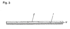
- Fig. 3 is a sectional view of copper foil 201, another metal foil of the circuit-forming board of the embodiment. Copper foil 201 is used instead of copper foil 1 shown in Fig. 1A. Instead of pressure absorption portion 1a, deformable layer 6 is formed at a surface of foil 201 opposite to a surface facing material sheet 2. The thickness of a portion of deformable layer 6 having a pressure applied thereto changes locally, similarly to pressure absorption portion 1a. Copper foil 201 includes hard portion 1G adjacent to deformable layer 6. Hard portion 1G is harder than deformable layer 6.
- Deformable layer 6 deforms during the heating and pressing, and preferably, has a hardness smaller than that of copper foil 201.
- Deformable layer 6 may be made of various material, such as organic material or inorganic material. Deformable layer 6, being made of inorganic material, produces less impurities or volatile components when it is heated.
- Deformable layer 6 may be made of epoxy resin or silicon resin having a large thermal resistance on copper foil 201 by casting method or a curtain coat technique to have a thickness of about 10 ⁇ m, having the same effects as those of pressure absorption portion 1a.
- a circuit-forming board without conductive paste such as a circuit-forming board including copper foil 1 and a conductive portion formed in via-hole 8 by plating, provides the same effects as those of the board of the embodiment.
- copper foil 1 is heated and pressed onto the conductive portion, the conductive portion is prevented from damage due to a pressure.
- Material sheet 2 may be a pre-preg sheet formed of glass fiber sheet, such as woven fabric or non-woven fabric, impregnated with thermosetting resin in a B-stage.
- glass fiber sheet such as woven fabric or non-woven fabric
- an organic fiber sheet such as an aramid sheet
- material sheet 2 instead of the fiber sheet, may be a B-stage film or a B-stage sheet composed of a resin film, such as a polyimide film, and an adhesive material.
- material sheet 2 may be a pre-preg sheet made of combined material of woven fabric and non-woven fabric as the reinforcing member.
- material sheet 2 may be a pre-preg sheet including two woven fabrics of glass fiber and a non-woven fabric of glass fiber between the woven fabrics.
- thermosetting resin in accordance with the embodiment may be epoxy resin, epoxy-melamine resin, unsaturated polyester resin, phenol resin, polyimide resin, cyanate resin, cyanate ester resin, naphthalene resin, urea resin, amino resin, alkyd resin, silicone resin, furan resin, polyurethane resin, aminoalkyd resin, acrylic resin, fluororesin, polyphenylene ether resin, cyanate ester resin, or mixture of two or more of the above resins.
- the thermosetting resin may have a composition modified by thermoplastic resin.
- fire retarding material or inorganic filler may be added into the thermosetting resin.
- Copper foil 1 or 201 in accordance with the embodiment may not necessarily be used for all layers of the multi-layer circuit board. In a layer of the layers near the outside of the board, a conductive portion for connecting circuit patterns (copper foils) of different layers are likely to be damaged, and therefore, copper foil 1 or 201 in accordance with the embodiment may be used for the layer near the outside. That is, copper foil 1 or 201 may be used only for tenth layer or eighth and tenth layers of a circuit board having ten layers, providing the same effects as those of the board of the embodiment.
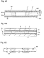
- Figs. 4A to 4C are sectional views of another circuit-forming board for illustrating a method of manufacturing the board in accordance with the embodiment.
- pressure absorption portion 1a is provided at surface 1C of copper foil 1 opposite to a surface facing material sheet 2.
- copper foil 501 of a metal foil has surface 501B facing material sheet 2 and has surface 501C opposite to surface 501B.
- Pressure absorption portion 501a is provided at surface portion 501G including surface 501B of copper foil 501.
- Pressure absorption portion 501a is provided with a roughness Rz of, e.g. 5 ⁇ m.
- Copper foil 501 has hard portion 501F adjacent to pressure absorption portion 501a, and hard portion is harder than pressure absorption portion 501a.
- Fig. 4B similarly to Fig. 1B, copper foils 501 and material sheet 2 are sandwiched between metal plates 4, and a pressure is applied in thickness direction 2A.
- Pressure absorption portion 501a has a thickness in the direction 2A changing according to the pressure applied to it, thus providing the same effects as those of pressure absorption portion 1a shown in Fig. 1B.
- copper foil 501 is processed, for example, by etching to form circuit pattern 505.
- the conductive paste used as the conductive portion connected to the copper foil may be made of mixture of conductive particles and polymer molecule material having a appropriate viscosity so that the paste may be released into material sheet 2 during the heating and pressing, mixture obtained by kneading conductive particles and solvent, or anisotropic conductive adhesive material.
- the conductive portion formed in via-hole 8 and connected to the copper foil may employ, instead of the conductive paste, a conductive protrusion having a post shape formed by, for example, plating, or conductive particles having large particle sizes which are not formed into a paste.
- a method of manufacturing a circuit-forming board in accordance with the present invention allows a material sheet, a metal foil, and a conductive portion, such as a conductive paste, in a via-hole formed in the material sheet to be heated and pressed, preventing the conductive portion from damage.
- This method provides a reliable electrical connection between the metal foil and the conductive portion, thus providing a circuit board with a high density and high quality.
Abstract
Description
- The present invention relates to a method of manufacturing a circuit-forming board for providing a circuit board used in various electronic equipment, and to a material for manufacturing the circuit-forming board.
- As electronic equipment has recently had a small size and a high density, circuit boards having electronic components mounted thereon shift from single-sided circuit boards to double-sided, multi-layer circuit boards. High-density circuit boards capable of integrating an increasing number of circuits and components have accordingly developed.
- Figs. 5A to 5G are sectional views of a conventional circuit-forming board providing a circuit board for illustrating a method of manufacturing the board disclosed in Japanese Patent Laid-Open Publication No.6-268345.
- As shown in Fig. 5A,
films 17 are attached onto both surfaces ofpre-preg sheet 12 by a laminating method using, e.g. a thermal roll. Pre-pregsheet 12 is obtained by drying woven fabric of glass fiber (reinforcing material) impregnated with varnish of thermosetting resin, such as epoxy resin.Pre-preg sheet 12 is in a B-stage and has a thickness of 100µm.Film 17 is made of polyethylene terephthalate (PET) having a thickness of 20µm.Film 17 may be coated with thermosetting resin, such as epoxy resin. - As shown in Fig. 5B, via-
holes 18 are formed in pre-pregsheet 12 by a process, such as a laser technology. - Next, as shown in Fig. 5C, via-
holes 18 are filled withconductive pastes 13 obtained by kneading thermosetting resin, hardening agent, solvent, and conductive particles, such as copper powder, - Then, as shown in Fig. 5D,
films 17 are peeled off.Conductive pastes 13 protrude from pre-pregsheet 12. Then,copper foils 19 are placed on both surfaces ofpre-preg sheet 12. - Then,
copper foils 19 are pressed by a hot-pressing apparatus (not shown) so as to heat pre-pregsheet 12,copper foils 19, andconductive pastes 13. This operation hardens pre-pregsheet 12 thermally, and compressesconductive pastes 13 as to allowconductive pastes 13 to be electrically connected tocopper foils 19, as shown in Fig. 5E. At this moment, the resin impregnated inpre-preg sheet 12 flows to outsides of pre-pregsheet 12, providingresin 12A. - Then, as shown in Fig. 5F, an unnecessary portion at an end is cut off, thus providing the circuit-forming board. Then,
copper foils 19 are etched to have predetermined circuit patterns to providecircuit patterns 15 shown in Fig. 5G, thereby providing a double-sided circuit board. This board is cut to providecircuit board 16 having a predetermined size. A solder resist may be formed oncircuit pattern 15 in order to prevent the pattern from having an unnecessary solder attached thereto.Circuit patterns 15 may be subjected to a finishing process, such as plating process. - Figs. 6A to 6E are sectional views of a multi-layer circuit board obtained with using
circuit board 16 manufactured by the method shown in Figs. 5A to 5G for illustrating a method of manufacturing the multi-layer circuit board. Pre-pregsheets 12B filled with conductive pastes 13A andcopper foils 19A are positioned and placed on both surfaces ofcircuit board 16 as a core, and are heated and pressed as to providemulti-layer circuit board 20 havingcircuit patterns 15A on both surfaces thereof. - In the method of manufacturing the circuit board shown in Figs. 5A to 5G,
conductive pastes 13 and 13A heated and pressed by, e.g. a hot-press apparatus may cause the following problem. Figs. 7A to 7C are sectional views of the circuit-forming board shown in Figs. 5A to 5G. As shown in Fig. 7A,copper foils 19 are placed on both surfaces ofpre-preg sheet 12 having via-holes 18 filled withconductive pastes 13. These are sandwiched betweenmetal plates 14, heated, and pressing, being compressed. A pressure applied to them may causeconductive pastes 13 to deform, distorting the shapes ofpastes 13, as shown in Fig. 7B - Then, as shown in Fig. 7C,
circuit patterns 15 are formed, andconductive pastes 13 become interlayer-connectingportions interlayer connecting portions conductive pastes 13, thereby reducing electrical insulation between the pastes. - When pre-preg
sheet 12 is heated and pressed, the resin impregnated into pre-pregsheet 12 flows. When an excessive pressure is applied toconductive paste 13,conductive pastes 13 spread in in-plane direction 12D more than inthickness direction 12C. Thereby, the conductive particles inconductive pastes 13 are not pressed strongly and do not contact each other, so that sufficient electrical connection cannot be obtained. This phenomenon appears significantly if the diameter of each via-hole 18 is smaller than the thickness ofpre-preg sheet 12. - As shown in Figs. 6A to 6E,
circuit board 16 as the core has a rough surface provided bycircuit patterns 15 and has an uneven thickness, during the manufacturing ofmulti-layer circuit board 20. The rough surfaces and the uneven thickness ofcircuit board 16 cause conductive paste 13A on the both surfaces to be compressed unstably by the heating and pressing, thereby causingconductive paste 13 to deform more easily. - A conductive portion is formed in a hole formed in a material sheet. A metal foil is placed on a surface of the material sheet to provide a laminated sheet. The laminated sheet is heated and pressed to provide a circuit-forming board. The metal foil includes a pressure absorption portion and a hard portion adjacent to the pressure absorption portion. The pressure absorption portion has a thickness changing according to a pressure applied thereto.
- The circuit-forming board provided by this method provides a high-density circuit board of high quality having reliable electrical connection.
-
- Fig. 1A is a sectional view of a circuit-forming board for illustrating a method of manufacturing the board in accordance with an exemplary embodiment of the present invention.
- Fig. 1B is a sectional view of the circuit-forming board for illustrating the method of manufacturing the board in accordance with the embodiment.
- Fig. 1C is a sectional view of the circuit-forming board for illustrating the method of manufacturing the board in accordance with the embodiment.
- Fig. 1D is a sectional view of the circuit-forming board for illustrating the method of manufacturing the board in accordance with the embodiment.
- Fig. 1E is a schematic view of a processing apparatus for processing a metal foil used in the circuit-forming board in accordance with the embodiment.
- Fig. 2A is a sectional view of a circuit board for illustrating a method of manufacturing the board in accordance with the embodiment.
- Fig. 2B is a sectional view of the circuit board for illustrating the method of manufacturing the board in accordance with the embodiment.
- Fig. 2C is a sectional view of the circuit board for illustrating the method of manufacturing the board in accordance with the embodiment.
- Fig. 2D is a sectional view of the circuit board for illustrating the method of manufacturing the board in accordance with the embodiment.
- Fig. 2E is a sectional view of the circuit board for illustrating the method of manufacturing the board in accordance with the embodiment.
- Fig. 3 is a sectional view of another metal foil of the circuit board in accordance with the embodiment.
- Fig. 4A is a sectional view of another circuit-forming board for illustrating a method of manufacturing the board in accordance with the embodiment.
- Fig. 4B is a sectional view of another circuit-forming board for illustrating the method of manufacturing the board in accordance with the embodiment.
- Fig. 4C is a sectional view of another circuit-forming board for illustrating the method of manufacturing the board in accordance with the embodiment.
- Fig. 5A is a sectional view of a conventional circuit-forming board for illustrating a method of manufacturing the board.
- Fig. 5B is a sectional view of the conventional circuit-forming board for illustrating the method of manufacturing the board.
- Fig. 5C is a sectional view of the conventional circuit-forming board for illustrating the method of manufacturing the board.
- Fig. 5D is a sectional view of the conventional circuit-forming board for illustrating the method of manufacturing the board.
- Fig. 5E is a sectional view of the conventional circuit-forming board for illustrating the method of manufacturing the board.
- Fig. 5F is a sectional view of the conventional circuit-forming board for illustrating the method of manufacturing the board.
- Fig. 5G is a sectional view of the conventional circuit-forming board for illustrating the method of manufacturing the board.
- Fig. 6A is a sectional view of a conventional circuit board for illustrating a method of manufacturing the board.
- Fig. 6B is a sectional view of the conventional circuit board for illustrating the method of manufacturing the board.
- Fig. 6C is a sectional view of the conventional circuit board for illustrating the method of manufacturing the board.
- Fig. 6D is a sectional view of the conventional circuit board for illustrating the method of manufacturing the board.
- Fig. 6E is a sectional view of the conventional circuit board for illustrating the method of manufacturing the board.
- Fig. 7A is a sectional view of the conventional circuit-forming board for illustrating the method of manufacturing the board.
- Fig. 7B is a sectional view of the conventional circuit-forming board for illustrating the method of manufacturing the board.
- Fig. 7C is a sectional view of the conventional circuit-forming board for illustrating the method of manufacturing the board.
-
-
- 1
- Copper Foil
- 1a
- Pressure Absorption Portion
- 2
- Material Sheet
- 3
- Conductive Paste
- 4
- Metal Plate
- 5
- Circuit Pattern
- 6
- Deformable Layer
- 10
- Circuit Board
- Figs. 1A to 1D are sectional views of a circuit-forming board for illustrating a method of manufacturing the board and a material for manufacturing a circuit board in accordance with an exemplary embodiment of the present invention. Fig. 1E is a schematic view of a processing apparatus for processing
copper foil 1 used in the circuit board.Copper foil 1 as a metal foil for manufacturing the circuit-forming board of the embodiment has a thickness of 18µm.Copper foil 1, a material for manufacturing the circuit-forming board, passes through aqueous solution 1102 of copper sulfate while being conveyed with cathode drum 1101. At this moment, an amount of copper is electrodeposited and grown by electrolytic action onsurface 1B ofcopper foil 1 which does not contact cathode drum 1101, and forms a roughness, thus providingsurface 1B with a roughness of a 10-point average roughness (Rz) of about 10µm. Bump-shaped members of copper are provided onsurface 1C ofcopper foil 1 which opposes to surface 1B and contacts cathode drum 1101 to roughensurface 1C, thus providingsurface 1C with a roughness Rz of about 5µm. Thus,copper foil 1 haspressure absorption portion 1a formed ofrough surface 1C. Similarly topre-preg sheet 12 shown in Figs. 5A to 5D, films are attached onto both surfaces ofmaterial sheet 2. Via-hole 8 is formed by, e.g. a laser processing, and is filled withconductive paste 3. Then, the films are peeled off. Thus,conductive paste 3 protrudes from the surfaces ofmaterial sheet 2. The films are attached onto the both surfaces ofmaterial sheet 2 by a laminating method using, e.g. a thermal roll.Material sheet 2 is obtained by drying woven fabric of glass fiber (a reinforcing member) impregnated with varnish of thermosetting resin, such as epoxy resin.Material sheet 2 is a pre-preg sheet in a B-stage having a thickness of 100µm.Material sheet 2 in accordance with the embodiment, even including the woven fabric of glass fiber, preventsconductive paste 3 from damages due to the displacement of yarns constituting the woven fabric at the heating and pressing. The films are made of polyethylene terephthalate (PET) having thicknesses of 20µm. The films may be coated with thermosetting resin, such as epoxy resin.Conductive paste 3 is obtained by kneading thermosetting resin, hardening agent, solvent, and conductive particles, such as copper powder. - As shown in Fig. 1A, copper foils 1 are placed on
material sheet 2 having via-hole 8 therein filled withconductive paste 3. - Then, as shown in Fig. 1B,
material sheet 2 and copper foils 1 is placed betweenmetal plates 4, such as SUS plates, as to be integrated with each other by heating and pressing, providinglaminated sheet 10B.Surface 1B of copper foil 1 (having a roughness Rz of about 10µm) facesmaterial sheet 2.Surface 1C (having a roughness Rz of about 5µm) functions aspressure absorption portion 1a. The roughnesses ofsurfaces copper foil 1 are not limited particularly to these values, and the roughness ofsurface 1B facingmaterial sheet 2 is preferably greater than that ofsurface 1C opposite tosurface 1B. During the heating and pressing,pressure absorption portion 1a ofsurface 1C ofcopper foil 1 is crushed to absorb a pressure applied to it. Therefore, the pressure is not concentrated overconductive paste 3 protruding frommaterial sheet 2. Thereby,conductive paste 3 is compressed inthickness direction 2A whilepaste 3 does not spread in in-plane direction 2B, thus avoiding the problem of the conventional circuit-forming board shown in Fig. 7B. That is,surface portion 1F ofcopper foil 1 includingsurface 1C corresponds to pressureabsorption portion 1a.Copper foil 1 hashard portion 1G adjacent to pressureabsorption portion 1a. - During the heating and pressing shown in Fig. 1B,
pressure absorption portion 1a ofcopper foil 1 is crushed, so that the resin flows from a portion ofmaterial sheet 2, reducing the thickness of the portion ofmaterial 2. Then, the height ofportion 1D ofcopper foil 1 on the portion ofmaterial sheet 2 becomes substantially identical to the height ofportion 1E ofcopper foil 1 onconductive paste 3. From this moment, a pressure is applied effectively toconductive paste 3 as to press conductive particles inconductive paste 3 to contactsurface 1B, being electrically connected withsurface 1B stably. That is, the thickness of a portion ofpressure absorption portion 1a having the pressure applied thereto changes locally, thus providing the circuit-forming board of the embodiment. - Next, as shown in Fig. 1C,
copper foil 1 is, for example, etched to formcircuit pattern 5 having a predetermined shape, thus providingcircuit board 10A. - Then, as shown in Fig. 1D,
pressure absorption portions 1a of a surface ofcircuit pattern 5 is removed by buffing or slight etching to increase a wettability to soldering, thus providingcircuit board 10. In order to further increase the wettability to soldering,circuit pattern 5 may be subjected to a finishing process, such as a plating process. - A solder resist may be formed on
circuit pattern 5 in order to preventpattern 5 from having an unnecessary solder attached thereto.Pressure absorption portion 1a may be removed after the solder resist is formed.Pressure absorption portion 1a may be removed beforecircuit pattern 5 is formed by etching. - The circuit-forming board provided by this method has a high density and a high quality.
Conductive paste 3 is compressed stably to be reliably connected withcopper foil 1 even if the diameter of via-hole 8 is small. - Figs. 2A to 2E are sectional views of a multi-layer circuit board for illustrating a method of manufacturing the board in accordance with the embodiment.
- As shown in Fig. 2A,
circuit board 10A shown in Fig. 1C is prepared as a core board.Pressure absorption portion 1a, a rough surface, remains on the surface ofcircuit pattern 5 ofcircuit board 10A - Next, as shown in Figs. 2B to 2D,
material sheets 2C filled withconductive paste 3A and copper foils 101 are placed on the both surfaces ofcircuit board 10A havingpressure absorption portions 101a, and they are integrated with each other by heating and pressing. Then, as shown in Fig. 2E,copper foil 101 is etched to formcircuit pattern 5A, thereby providingmulti-layer circuit board 10B. -
Pressure absorption portion 1a remains on the surface ofcircuit pattern 5A ofcircuit board 10A as the core board as to provide the surface with a roughness. This roughness increases an adhesive strength betweencopper foil 1 andconductive paste 3A. - Fig. 3 is a sectional view of copper foil 201, another metal foil of the circuit-forming board of the embodiment. Copper foil 201 is used instead of
copper foil 1 shown in Fig. 1A. Instead ofpressure absorption portion 1a, deformable layer 6 is formed at a surface of foil 201 opposite to a surface facingmaterial sheet 2. The thickness of a portion of deformable layer 6 having a pressure applied thereto changes locally, similarly topressure absorption portion 1a. Copper foil 201 includeshard portion 1G adjacent to deformable layer 6.Hard portion 1G is harder than deformable layer 6. - Deformable layer 6 deforms during the heating and pressing, and preferably, has a hardness smaller than that of copper foil 201. Deformable layer 6 may be made of various material, such as organic material or inorganic material. Deformable layer 6, being made of inorganic material, produces less impurities or volatile components when it is heated. Deformable layer 6 may be made of epoxy resin or silicon resin having a large thermal resistance on copper foil 201 by casting method or a curtain coat technique to have a thickness of about 10µm, having the same effects as those of
pressure absorption portion 1a. - A circuit-forming board without conductive paste, such as a circuit-forming board including
copper foil 1 and a conductive portion formed in via-hole 8 by plating, provides the same effects as those of the board of the embodiment. Whencopper foil 1 is heated and pressed onto the conductive portion, the conductive portion is prevented from damage due to a pressure. -
Material sheet 2 may be a pre-preg sheet formed of glass fiber sheet, such as woven fabric or non-woven fabric, impregnated with thermosetting resin in a B-stage. Instead of the glass fiber sheet, an organic fiber sheet, such as an aramid sheet, may be used. Furthermore,material sheet 2, instead of the fiber sheet, may be a B-stage film or a B-stage sheet composed of a resin film, such as a polyimide film, and an adhesive material. - Furthermore,
material sheet 2 may be a pre-preg sheet made of combined material of woven fabric and non-woven fabric as the reinforcing member. For example,material sheet 2 may be a pre-preg sheet including two woven fabrics of glass fiber and a non-woven fabric of glass fiber between the woven fabrics. - The thermosetting resin in accordance with the embodiment may be epoxy resin, epoxy-melamine resin, unsaturated polyester resin, phenol resin, polyimide resin, cyanate resin, cyanate ester resin, naphthalene resin, urea resin, amino resin, alkyd resin, silicone resin, furan resin, polyurethane resin, aminoalkyd resin, acrylic resin, fluororesin, polyphenylene ether resin, cyanate ester resin, or mixture of two or more of the above resins. Alternatively, the thermosetting resin may have a composition modified by thermoplastic resin. Furthermore, if necessary, fire retarding material or inorganic filler may be added into the thermosetting resin.
-
Copper foil 1 or 201 in accordance with the embodiment may not necessarily be used for all layers of the multi-layer circuit board. In a layer of the layers near the outside of the board, a conductive portion for connecting circuit patterns (copper foils) of different layers are likely to be damaged, and therefore,copper foil 1 or 201 in accordance with the embodiment may be used for the layer near the outside. That is,copper foil 1 or 201 may be used only for tenth layer or eighth and tenth layers of a circuit board having ten layers, providing the same effects as those of the board of the embodiment. - Figs. 4A to 4C are sectional views of another circuit-forming board for illustrating a method of manufacturing the board in accordance with the embodiment. In the circuit-forming board shown in Figs. 1A to 1D,
pressure absorption portion 1a is provided atsurface 1C ofcopper foil 1 opposite to a surface facingmaterial sheet 2. As shown in Fig. 4A,copper foil 501 of a metal foil hassurface 501B facingmaterial sheet 2 and hassurface 501C opposite to surface 501B.Pressure absorption portion 501a is provided atsurface portion 501G including surface 501B ofcopper foil 501.Pressure absorption portion 501a is provided with a roughness Rz of, e.g. 5µm.Copper foil 501 hashard portion 501F adjacent to pressureabsorption portion 501a, and hard portion is harder thanpressure absorption portion 501a. As shown in Fig. 4B, similarly to Fig. 1B, copper foils 501 andmaterial sheet 2 are sandwiched betweenmetal plates 4, and a pressure is applied inthickness direction 2A.Pressure absorption portion 501a has a thickness in thedirection 2A changing according to the pressure applied to it, thus providing the same effects as those ofpressure absorption portion 1a shown in Fig. 1B. Then,copper foil 501 is processed, for example, by etching to formcircuit pattern 505. - The conductive paste used as the conductive portion connected to the copper foil may be made of mixture of conductive particles and polymer molecule material having a appropriate viscosity so that the paste may be released into
material sheet 2 during the heating and pressing, mixture obtained by kneading conductive particles and solvent, or anisotropic conductive adhesive material. - The conductive portion formed in via-hole 8 and connected to the copper foil may employ, instead of the conductive paste, a conductive protrusion having a post shape formed by, for example, plating, or conductive particles having large particle sizes which are not formed into a paste.
- A method of manufacturing a circuit-forming board in accordance with the present invention allows a material sheet, a metal foil, and a conductive portion, such as a conductive paste, in a via-hole formed in the material sheet to be heated and pressed, preventing the conductive portion from damage. This method provides a reliable electrical connection between the metal foil and the conductive portion, thus providing a circuit board with a high density and high quality.
Claims (17)
- A method of manufacturing a circuit-forming board, comprising:providing a metal foil having a first surface and a second surface opposite to the first surface, the metal foil including a pressure absorption portion and a hard portion adjacent to the pressure absorption portion, the pressure absorption portion being provided at the first surface, the pressure absorption portion having a thickness changing according to a pressure applied thereto;providing a material sheet having a surface, the surface having a hole formed therein;forming a conductive portion in the hole of the material sheet;providing a laminated sheet by placing the metal foil on the surface of the material sheet; andheating and pressing the laminated sheet.
- The method according to claim 1, wherein the hard portion is harder than the pressure absorption portion.
- The method according to claim 1, wherein said providing the laminated sheet comprises allowing the second surface of the metal foil to face the material sheet.
- The method according to claim 1, wherein the first surface of the metal foil is roughened, and the pressure absorption portion comprises a surface portion of the metal foil including the first surface of the metal foil.
- The method according to claim 4,
wherein said providing the laminated sheet comprises allowing the second surface of the metal foil to face the material sheet,
wherein said providing the metal foil comprises roughening the second surface of the metal foil, and
wherein the second surface of the metal foil is rougher than the first surface of the metal foil. - The method according to claim 1, wherein the pressure absorption portion comprises deformable organic material.
- The method according to claim 1, wherein the pressure absorption portion comprises deformable inorganic material.
- The method according to claim 1, further comprising removing the pressure absorption portion after said heating and pressing the laminated sheet.
- The method according to claim 1, wherein said forming the conductive portion in the hole of the material sheet comprises filling the hole of the material sheet with a conductive paste.
- The method according to claim 1, wherein said providing the laminated sheet comprises allowing the first surface of the metal foil to face the material sheet.
- A material for manufacturing a circuit-forming board, said material comprising:wherein the circuit-forming board comprises a material sheet having a surface having a hole formed therein and a conductive portion provided in the hole; anda pressure absorption portion having a thickness changing according to a pressure applied thereto; anda metal foil having a first surface and a second surface opposite to the first surface, the pressure absorption portion being provided on the first surface, the metal foil including a hard portion adjacent to the pressure absorption portion,
wherein said material is arranged to be placed on the surface of the material sheet and pressed together with the material sheet and the conductive portion. - The material according to claim 11, wherein the hard portion is harder than the pressure absorption portion.
- The material according to claim 11, wherein the second surface of the metal foil is arranged to face the material sheet.
- The material according to claim 11, wherein the first surface of the metal foil is roughened, and the pressure absorption portion is a surface portion including the first surface of the metal foil.
- The material according to claim 14,
wherein the second surface of the metal foil is arranged to face the material sheet,
wherein the second surface of the metal foil is roughened; and
wherein the second surface of the metal foil is rougher than the first surface of the metal foil. - The material according to claim 11, wherein the pressure absorption portion comprises deformable organic material.
- The material according to claim 11, wherein the pressure absorption portion comprises deformable inorganic material.
Applications Claiming Priority (3)
| Application Number | Priority Date | Filing Date | Title |
|---|---|---|---|
| JP2004016795 | 2004-01-26 | ||
| JP2004016795A JP3979391B2 (en) | 2004-01-26 | 2004-01-26 | Circuit forming substrate manufacturing method and circuit forming substrate manufacturing material |
| PCT/JP2005/000763 WO2005072037A1 (en) | 2004-01-26 | 2005-01-21 | Method for producing circuit-forming board and material for producing circuit-forming board |
Publications (3)
| Publication Number | Publication Date |
|---|---|
| EP1599079A1 true EP1599079A1 (en) | 2005-11-23 |
| EP1599079A4 EP1599079A4 (en) | 2008-05-21 |
| EP1599079B1 EP1599079B1 (en) | 2012-05-09 |
Family
ID=34805507
Family Applications (1)
| Application Number | Title | Priority Date | Filing Date |
|---|---|---|---|
| EP05703984A Expired - Fee Related EP1599079B1 (en) | 2004-01-26 | 2005-01-21 | Method for producing a circuit board and material for producing a circuit board |
Country Status (7)
| Country | Link |
|---|---|
| US (2) | US7624502B2 (en) |
| EP (1) | EP1599079B1 (en) |
| JP (1) | JP3979391B2 (en) |
| KR (1) | KR100736518B1 (en) |
| CN (1) | CN100539813C (en) |
| TW (1) | TW200527995A (en) |
| WO (1) | WO2005072037A1 (en) |
Families Citing this family (12)
| Publication number | Priority date | Publication date | Assignee | Title |
|---|---|---|---|---|
| JP4903723B2 (en) * | 2006-01-30 | 2012-03-28 | 京セラ株式会社 | Wiring board and electronic device |
| KR100905566B1 (en) * | 2007-04-30 | 2009-07-02 | 삼성전기주식회사 | Carrier member for transmitting circuits, coreless printed circuit board using the said carrier member, and methods of manufacturing the same |
| CN101562952B (en) * | 2008-04-18 | 2012-04-11 | 富葵精密组件(深圳)有限公司 | Circuit substrate, manufacture method of circuit substrate and manufacture method of circuit wafer |
| KR100999918B1 (en) * | 2008-09-08 | 2010-12-13 | 삼성전기주식회사 | Printed circuit board and method of manufacturing the same |
| KR100982791B1 (en) * | 2010-07-08 | 2010-09-16 | 윤병철 | Method for applying an electric connect from the upper side to the lower side of the insulator in non-pcb composite plate in use of metallic staple |
| KR100982790B1 (en) * | 2010-07-08 | 2010-09-16 | 윤병철 | Method for applying an electric connect from the upper side to the lower side of the insulator in non-pcb composite plate in use of metallic fiber |
| GB2529346A (en) | 2011-03-31 | 2016-02-17 | Plasyl Ltd | Improvements for electrical circuits |
| TW201340807A (en) * | 2011-12-28 | 2013-10-01 | Panasonic Corp | Flexible wiring board, method for manufacturing flexible wiring board, package product using flexible wiring board, and flexible multilayer wiring board |
| KR101494090B1 (en) * | 2013-07-16 | 2015-02-16 | 삼성전기주식회사 | Copper clad laminate, printed circuit board and method for manufacturing of the same |
| CN104768326B (en) * | 2015-03-31 | 2017-11-24 | 华为技术有限公司 | Printed circuit board (PCB) and board, printed circuit board manufacturing method |
| DE102018125919A1 (en) | 2017-10-23 | 2019-04-25 | Engel Austria Gmbh | Method for moving a movable platen |
| CN115837792B (en) * | 2022-12-12 | 2023-07-11 | 广东嘉元科技股份有限公司 | Automatic copper foil bonding device |
Citations (4)
| Publication number | Priority date | Publication date | Assignee | Title |
|---|---|---|---|---|
| US5413838A (en) * | 1991-06-18 | 1995-05-09 | Sumitomo Bakelite Company Limited | Both-side roughened copper foil with protection film |
| JPH0946041A (en) * | 1995-07-26 | 1997-02-14 | Toshiba Corp | Manufacture of printed wiring board |
| US20030039811A1 (en) * | 2001-01-15 | 2003-02-27 | Toshio Sugawa | Circuit board and production method thereof |
| JP2003209355A (en) * | 2002-01-15 | 2003-07-25 | Sony Corp | Circuit board and method for manufacturing the same |
Family Cites Families (26)
| Publication number | Priority date | Publication date | Assignee | Title |
|---|---|---|---|---|
| JPS63170994A (en) * | 1986-05-30 | 1988-07-14 | 古河電気工業株式会社 | Multilayer printed interconnection board and manufacture of the same |
| JPH07115280B2 (en) * | 1986-10-21 | 1995-12-13 | 日立精機株式会社 | Unbalanced tool measuring device |
| US5344893A (en) * | 1991-07-23 | 1994-09-06 | Ibiden Co., Ltd. | Epoxy/amino powder resin adhesive for printed circuit board |
| JP2601128B2 (en) | 1992-05-06 | 1997-04-16 | 松下電器産業株式会社 | Method of manufacturing circuit forming substrate and circuit forming substrate |
| US5403672A (en) * | 1992-08-17 | 1995-04-04 | Hitachi Chemical Co., Ltd. | Metal foil for printed wiring board and production thereof |
| JP3146712B2 (en) * | 1993-01-12 | 2001-03-19 | 松下電器産業株式会社 | Double-sided printed circuit board and method of manufacturing the same |
| US5779870A (en) * | 1993-03-05 | 1998-07-14 | Polyclad Laminates, Inc. | Method of manufacturing laminates and printed circuit boards |
| US5519177A (en) * | 1993-05-19 | 1996-05-21 | Ibiden Co., Ltd. | Adhesives, adhesive layers for electroless plating and printed circuit boards |
| JP3173249B2 (en) * | 1993-10-20 | 2001-06-04 | 松下電器産業株式会社 | Multilayer printed wiring board and method of manufacturing the same |
| US5652042A (en) * | 1993-10-29 | 1997-07-29 | Matsushita Electric Industrial Co., Ltd. | Conductive paste compound for via hole filling, printed circuit board which uses the conductive paste |
| US5482784A (en) * | 1993-12-24 | 1996-01-09 | Mitsui Mining And Smelting Co., Ltd. | Printed circuit inner-layer copper foil and process for producing the same |
| JP3311899B2 (en) * | 1995-01-20 | 2002-08-05 | 松下電器産業株式会社 | Circuit board and method of manufacturing the same |
| US6010768A (en) * | 1995-11-10 | 2000-01-04 | Ibiden Co., Ltd. | Multilayer printed circuit board, method of producing multilayer printed circuit board and resin filler |
| US6085414A (en) * | 1996-08-15 | 2000-07-11 | Packard Hughes Interconnect Company | Method of making a flexible circuit with raised features protruding from two surfaces and products therefrom |
| EP1035758B1 (en) * | 1997-04-15 | 2003-03-19 | Ibiden Co, Ltd. | Adhesive for electroless plating, raw material composition for preparing adhesive for electroless plating and printed wiring board |
| US6239777B1 (en) * | 1997-07-22 | 2001-05-29 | Kabushiki Kaisha Toshiba | Display device |
| JPH11251703A (en) | 1998-02-27 | 1999-09-17 | Matsushita Electric Ind Co Ltd | Circuit board, both-sided circuit board, multilayered circuit board, and manufacture of circuit board |
| US6139777A (en) * | 1998-05-08 | 2000-10-31 | Matsushita Electric Industrial Co., Ltd. | Conductive paste for filling via-hole, double-sided and multilayer printed circuit boards using the same, and method for producing the same |
| JP4486196B2 (en) * | 1999-12-08 | 2010-06-23 | イビデン株式会社 | Single-sided circuit board for multilayer printed wiring board and manufacturing method thereof |
| US6504705B2 (en) * | 2000-10-12 | 2003-01-07 | Matsushita Electric Industrial Co., Ltd. | Electrolytic capacitor, circuit board containing electrolytic capacitor, and method for producing the same |
| US6713688B2 (en) * | 2000-12-27 | 2004-03-30 | Matsushita Electric Industrial Co., Ltd. | Circuit board and its manufacture method |
| JP2002368043A (en) * | 2001-06-12 | 2002-12-20 | Matsushita Electric Ind Co Ltd | Conductive paste, conductive bump using it, its forming method, method for connecting conductive bump, circuit board and its producing method |
| JP2003023250A (en) * | 2001-07-06 | 2003-01-24 | Denso Corp | Multilayered substrate and its manufacturing method |
| JP4062907B2 (en) * | 2001-11-12 | 2008-03-19 | 松下電器産業株式会社 | Circuit board and manufacturing method thereof |
| EP1357773A3 (en) * | 2002-04-25 | 2005-11-30 | Matsushita Electric Industrial Co., Ltd. | Wiring transfer sheet and method for producing the same, and wiring board and method for producing the same |
| JP4029759B2 (en) * | 2003-04-04 | 2008-01-09 | 株式会社デンソー | Multilayer circuit board and manufacturing method thereof |
-
2004
- 2004-01-26 JP JP2004016795A patent/JP3979391B2/en not_active Expired - Fee Related
-
2005
- 2005-01-19 TW TW094101542A patent/TW200527995A/en not_active IP Right Cessation
- 2005-01-21 CN CNB2005800002557A patent/CN100539813C/en not_active Expired - Fee Related
- 2005-01-21 EP EP05703984A patent/EP1599079B1/en not_active Expired - Fee Related
- 2005-01-21 WO PCT/JP2005/000763 patent/WO2005072037A1/en active Application Filing
- 2005-01-21 US US10/546,730 patent/US7624502B2/en not_active Expired - Fee Related
- 2005-01-21 KR KR1020057017222A patent/KR100736518B1/en not_active IP Right Cessation
-
2007
- 2007-08-01 US US11/882,396 patent/US7572500B2/en not_active Expired - Fee Related
Patent Citations (4)
| Publication number | Priority date | Publication date | Assignee | Title |
|---|---|---|---|---|
| US5413838A (en) * | 1991-06-18 | 1995-05-09 | Sumitomo Bakelite Company Limited | Both-side roughened copper foil with protection film |
| JPH0946041A (en) * | 1995-07-26 | 1997-02-14 | Toshiba Corp | Manufacture of printed wiring board |
| US20030039811A1 (en) * | 2001-01-15 | 2003-02-27 | Toshio Sugawa | Circuit board and production method thereof |
| JP2003209355A (en) * | 2002-01-15 | 2003-07-25 | Sony Corp | Circuit board and method for manufacturing the same |
Non-Patent Citations (1)
| Title |
|---|
| See also references of WO2005072037A1 * |
Also Published As
| Publication number | Publication date |
|---|---|
| CN1771773A (en) | 2006-05-10 |
| CN100539813C (en) | 2009-09-09 |
| JP2005209993A (en) | 2005-08-04 |
| KR100736518B1 (en) | 2007-07-06 |
| EP1599079A4 (en) | 2008-05-21 |
| WO2005072037A1 (en) | 2005-08-04 |
| US7624502B2 (en) | 2009-12-01 |
| TWI350718B (en) | 2011-10-11 |
| JP3979391B2 (en) | 2007-09-19 |
| US20060242827A1 (en) | 2006-11-02 |
| EP1599079B1 (en) | 2012-05-09 |
| TW200527995A (en) | 2005-08-16 |
| KR20050110001A (en) | 2005-11-22 |
| US7572500B2 (en) | 2009-08-11 |
| US20080017403A1 (en) | 2008-01-24 |
Similar Documents
| Publication | Publication Date | Title |
|---|---|---|
| US7572500B2 (en) | Method of manufacturing circuit-forming board and material of circuit-forming board | |
| US6946205B2 (en) | Wiring transfer sheet and method for producing the same, and wiring board and method for producing the same | |
| EP0961533B1 (en) | Circuit board and method of manufacturing the same | |
| EP1206171B1 (en) | Circuit board and method for manufacturing the same | |
| US20020023777A1 (en) | Printed circuit board and method for producing the same | |
| WO2001045478A1 (en) | Multilayered printed wiring board and production method therefor | |
| JP4075673B2 (en) | Copper-clad laminate for multilayer printed wiring board, multilayer printed wiring board, and method for manufacturing multilayer printed wiring board | |
| JPWO2007069510A1 (en) | Intermediate material for manufacturing circuit board and method for manufacturing circuit board using the same | |
| EP1267595A1 (en) | Circuit forming board producing method, circuit forming board, and material for circuit forming board | |
| US6523258B2 (en) | Method of manufacturing printed circuit board | |
| US7356916B2 (en) | Circuit-formed substrate and method of manufacturing circuit-formed substrate | |
| JP3587457B2 (en) | Circuit board and its manufacturing method | |
| JP4161604B2 (en) | Printed wiring board and manufacturing method thereof | |
| US8069557B2 (en) | Method of manufacturing circuit forming board |
Legal Events
| Date | Code | Title | Description |
|---|---|---|---|
| PUAI | Public reference made under article 153(3) epc to a published international application that has entered the european phase |
Free format text: ORIGINAL CODE: 0009012 |
|
| 17P | Request for examination filed |
Effective date: 20050822 |
|
| AK | Designated contracting states |
Kind code of ref document: A1 Designated state(s): AT BE BG CH CY CZ DE DK EE ES FI FR GB GR HU IE IS IT LI LT LU MC NL PL PT RO SE SI SK TR |
|
| AX | Request for extension of the european patent |
Extension state: AL BA HR LV MK YU |
|
| DAX | Request for extension of the european patent (deleted) | ||
| RBV | Designated contracting states (corrected) |
Designated state(s): DE FR GB |
|
| A4 | Supplementary search report drawn up and despatched |
Effective date: 20080417 |
|
| RIC1 | Information provided on ipc code assigned before grant |
Ipc: H05K 3/46 20060101AFI20050811BHEP Ipc: H05K 3/38 20060101ALI20080411BHEP Ipc: H05K 3/40 20060101ALI20080411BHEP |
|
| RAP1 | Party data changed (applicant data changed or rights of an application transferred) |
Owner name: PANASONIC CORPORATION |
|
| 17Q | First examination report despatched |
Effective date: 20100720 |
|
| RTI1 | Title (correction) |
Free format text: METHOD FOR PRODUCING A CIRCUIT BOARD AND MATERIAL FOR PRODUCING A CIRCUIT BOARD |
|
| GRAP | Despatch of communication of intention to grant a patent |
Free format text: ORIGINAL CODE: EPIDOSNIGR1 |
|
| GRAS | Grant fee paid |
Free format text: ORIGINAL CODE: EPIDOSNIGR3 |
|
| GRAA | (expected) grant |
Free format text: ORIGINAL CODE: 0009210 |
|
| AK | Designated contracting states |
Kind code of ref document: B1 Designated state(s): DE FR GB |
|
| REG | Reference to a national code |
Ref country code: GB Ref legal event code: FG4D |
|
| REG | Reference to a national code |
Ref country code: DE Ref legal event code: R096 Ref document number: 602005034095 Country of ref document: DE Effective date: 20120712 |
|
| PLBE | No opposition filed within time limit |
Free format text: ORIGINAL CODE: 0009261 |
|
| STAA | Information on the status of an ep patent application or granted ep patent |
Free format text: STATUS: NO OPPOSITION FILED WITHIN TIME LIMIT |
|
| 26N | No opposition filed |
Effective date: 20130212 |
|
| REG | Reference to a national code |
Ref country code: DE Ref legal event code: R097 Ref document number: 602005034095 Country of ref document: DE Effective date: 20130212 |
|
| PGFP | Annual fee paid to national office [announced via postgrant information from national office to epo] |
Ref country code: DE Payment date: 20140122 Year of fee payment: 10 |
|
| PGFP | Annual fee paid to national office [announced via postgrant information from national office to epo] |
Ref country code: FR Payment date: 20140123 Year of fee payment: 10 |
|
| PGFP | Annual fee paid to national office [announced via postgrant information from national office to epo] |
Ref country code: GB Payment date: 20140121 Year of fee payment: 10 |
|
| REG | Reference to a national code |
Ref country code: DE Ref legal event code: R119 Ref document number: 602005034095 Country of ref document: DE |
|
| GBPC | Gb: european patent ceased through non-payment of renewal fee |
Effective date: 20150121 |
|
| PG25 | Lapsed in a contracting state [announced via postgrant information from national office to epo] |
Ref country code: DE Free format text: LAPSE BECAUSE OF NON-PAYMENT OF DUE FEES Effective date: 20150801 Ref country code: GB Free format text: LAPSE BECAUSE OF NON-PAYMENT OF DUE FEES Effective date: 20150121 |
|
| REG | Reference to a national code |
Ref country code: FR Ref legal event code: ST Effective date: 20150930 |
|
| PG25 | Lapsed in a contracting state [announced via postgrant information from national office to epo] |
Ref country code: FR Free format text: LAPSE BECAUSE OF NON-PAYMENT OF DUE FEES Effective date: 20150202 |