JP3810076B2 - Information recording medium - Google Patents
Information recording mediumInfo
- Publication number
- JP3810076B2 JP3810076B2 JP2004509072A JP2004509072A JP3810076B2 JP 3810076 B2 JP3810076 B2 JP 3810076B2 JP 2004509072 A JP2004509072 A JP 2004509072A JP 2004509072 A JP2004509072 A JP 2004509072A JP 3810076 B2 JP3810076 B2 JP 3810076B2
- Authority
- JP
- Japan
- Prior art keywords
- nitride
- recording layer
- recording
- recording medium
- layer
- Prior art date
- Legal status (The legal status is an assumption and is not a legal conclusion. Google has not performed a legal analysis and makes no representation as to the accuracy of the status listed.)
- Expired - Lifetime
Links
Images


Classifications
-
- G—PHYSICS
- G11—INFORMATION STORAGE
- G11B—INFORMATION STORAGE BASED ON RELATIVE MOVEMENT BETWEEN RECORD CARRIER AND TRANSDUCER
- G11B7/00—Recording or reproducing by optical means, e.g. recording using a thermal beam of optical radiation by modifying optical properties or the physical structure, reproducing using an optical beam at lower power by sensing optical properties; Record carriers therefor
- G11B7/24—Record carriers characterised by shape, structure or physical properties, or by the selection of the material
- G11B7/26—Apparatus or processes specially adapted for the manufacture of record carriers
- G11B7/266—Sputtering or spin-coating layers
-
- B—PERFORMING OPERATIONS; TRANSPORTING
- B41—PRINTING; LINING MACHINES; TYPEWRITERS; STAMPS
- B41M—PRINTING, DUPLICATING, MARKING, OR COPYING PROCESSES; COLOUR PRINTING
- B41M5/00—Duplicating or marking methods; Sheet materials for use therein
- B41M5/26—Thermography ; Marking by high energetic means, e.g. laser otherwise than by burning, and characterised by the material used
-
- G—PHYSICS
- G11—INFORMATION STORAGE
- G11B—INFORMATION STORAGE BASED ON RELATIVE MOVEMENT BETWEEN RECORD CARRIER AND TRANSDUCER
- G11B7/00—Recording or reproducing by optical means, e.g. recording using a thermal beam of optical radiation by modifying optical properties or the physical structure, reproducing using an optical beam at lower power by sensing optical properties; Record carriers therefor
- G11B7/24—Record carriers characterised by shape, structure or physical properties, or by the selection of the material
- G11B7/241—Record carriers characterised by shape, structure or physical properties, or by the selection of the material characterised by the selection of the material
- G11B7/242—Record carriers characterised by shape, structure or physical properties, or by the selection of the material characterised by the selection of the material of recording layers
- G11B7/243—Record carriers characterised by shape, structure or physical properties, or by the selection of the material characterised by the selection of the material of recording layers comprising inorganic materials only, e.g. ablative layers
-
- G—PHYSICS
- G11—INFORMATION STORAGE
- G11B—INFORMATION STORAGE BASED ON RELATIVE MOVEMENT BETWEEN RECORD CARRIER AND TRANSDUCER
- G11B7/00—Recording or reproducing by optical means, e.g. recording using a thermal beam of optical radiation by modifying optical properties or the physical structure, reproducing using an optical beam at lower power by sensing optical properties; Record carriers therefor
- G11B7/24—Record carriers characterised by shape, structure or physical properties, or by the selection of the material
- G11B7/26—Apparatus or processes specially adapted for the manufacture of record carriers
-
- G—PHYSICS
- G11—INFORMATION STORAGE
- G11B—INFORMATION STORAGE BASED ON RELATIVE MOVEMENT BETWEEN RECORD CARRIER AND TRANSDUCER
- G11B7/00—Recording or reproducing by optical means, e.g. recording using a thermal beam of optical radiation by modifying optical properties or the physical structure, reproducing using an optical beam at lower power by sensing optical properties; Record carriers therefor
- G11B7/24—Record carriers characterised by shape, structure or physical properties, or by the selection of the material
- G11B7/241—Record carriers characterised by shape, structure or physical properties, or by the selection of the material characterised by the selection of the material
- G11B7/242—Record carriers characterised by shape, structure or physical properties, or by the selection of the material characterised by the selection of the material of recording layers
- G11B7/243—Record carriers characterised by shape, structure or physical properties, or by the selection of the material characterised by the selection of the material of recording layers comprising inorganic materials only, e.g. ablative layers
- G11B2007/24302—Metals or metalloids
- G11B2007/24306—Metals or metalloids transition metal elements of groups 3-10
-
- G—PHYSICS
- G11—INFORMATION STORAGE
- G11B—INFORMATION STORAGE BASED ON RELATIVE MOVEMENT BETWEEN RECORD CARRIER AND TRANSDUCER
- G11B7/00—Recording or reproducing by optical means, e.g. recording using a thermal beam of optical radiation by modifying optical properties or the physical structure, reproducing using an optical beam at lower power by sensing optical properties; Record carriers therefor
- G11B7/24—Record carriers characterised by shape, structure or physical properties, or by the selection of the material
- G11B7/241—Record carriers characterised by shape, structure or physical properties, or by the selection of the material characterised by the selection of the material
- G11B7/242—Record carriers characterised by shape, structure or physical properties, or by the selection of the material characterised by the selection of the material of recording layers
- G11B7/243—Record carriers characterised by shape, structure or physical properties, or by the selection of the material characterised by the selection of the material of recording layers comprising inorganic materials only, e.g. ablative layers
- G11B2007/24302—Metals or metalloids
- G11B2007/24312—Metals or metalloids group 14 elements (e.g. Si, Ge, Sn)
-
- G—PHYSICS
- G11—INFORMATION STORAGE
- G11B—INFORMATION STORAGE BASED ON RELATIVE MOVEMENT BETWEEN RECORD CARRIER AND TRANSDUCER
- G11B7/00—Recording or reproducing by optical means, e.g. recording using a thermal beam of optical radiation by modifying optical properties or the physical structure, reproducing using an optical beam at lower power by sensing optical properties; Record carriers therefor
- G11B7/24—Record carriers characterised by shape, structure or physical properties, or by the selection of the material
- G11B7/241—Record carriers characterised by shape, structure or physical properties, or by the selection of the material characterised by the selection of the material
- G11B7/242—Record carriers characterised by shape, structure or physical properties, or by the selection of the material characterised by the selection of the material of recording layers
- G11B7/243—Record carriers characterised by shape, structure or physical properties, or by the selection of the material characterised by the selection of the material of recording layers comprising inorganic materials only, e.g. ablative layers
- G11B2007/24302—Metals or metalloids
- G11B2007/24314—Metals or metalloids group 15 elements (e.g. Sb, Bi)
-
- G—PHYSICS
- G11—INFORMATION STORAGE
- G11B—INFORMATION STORAGE BASED ON RELATIVE MOVEMENT BETWEEN RECORD CARRIER AND TRANSDUCER
- G11B7/00—Recording or reproducing by optical means, e.g. recording using a thermal beam of optical radiation by modifying optical properties or the physical structure, reproducing using an optical beam at lower power by sensing optical properties; Record carriers therefor
- G11B7/24—Record carriers characterised by shape, structure or physical properties, or by the selection of the material
- G11B7/241—Record carriers characterised by shape, structure or physical properties, or by the selection of the material characterised by the selection of the material
- G11B7/242—Record carriers characterised by shape, structure or physical properties, or by the selection of the material characterised by the selection of the material of recording layers
- G11B7/243—Record carriers characterised by shape, structure or physical properties, or by the selection of the material characterised by the selection of the material of recording layers comprising inorganic materials only, e.g. ablative layers
- G11B2007/24318—Non-metallic elements
- G11B2007/24322—Nitrogen
-
- Y—GENERAL TAGGING OF NEW TECHNOLOGICAL DEVELOPMENTS; GENERAL TAGGING OF CROSS-SECTIONAL TECHNOLOGIES SPANNING OVER SEVERAL SECTIONS OF THE IPC; TECHNICAL SUBJECTS COVERED BY FORMER USPC CROSS-REFERENCE ART COLLECTIONS [XRACs] AND DIGESTS
- Y10—TECHNICAL SUBJECTS COVERED BY FORMER USPC
- Y10S—TECHNICAL SUBJECTS COVERED BY FORMER USPC CROSS-REFERENCE ART COLLECTIONS [XRACs] AND DIGESTS
- Y10S430/00—Radiation imagery chemistry: process, composition, or product thereof
- Y10S430/146—Laser beam
Description
技術分野
本発明は、光ビームの照射により情報の記録再生を行う光ディスク、光カードなどの光学式情報記録媒体及びその製造方法に関する。
背景技術
近年、DVD(Digital Versatile Disc)は、映像データ、音声データ及びコンピュータデータなどのデータを記録再生する情報記録媒体として広く用いられている。このDVDには、再生専用の他に、記録層に有機色素材料を用いて追記可能としたり(DVD−R(recordable))、相変化材料を記録層に用いて書き換え自在としたDVD−RW(re−recordable)などがある。
更なる高密度化において、635nmより短い波長域の光ビームで記録再生を行うことが要望されているが、従来のような追記型光ディスクにおいて、十分な光ディスク特性を実現できていない。
また、追記型光ディスクとして、レーザ光照射によって記録層に穴をあけたり、記録層中に風船状の空洞を作って膜を隆起させたり、熱分解生成物質を記録層中に分散させる物質を添加するものが報告されている。これら従来の記録方法では、高密度化に伴う微細な記録マークの形成においてはマークのサイズやエッジの制御が困難となる問題がある。すなわち図16に示すように、記録案内溝をはみ出す大きなマークとして変形などを伴って記録を行っている。
追記型光ディスクは、一度記録した部位には再書込みできないので、消費量が多くなり、廃棄時の環境への影響を考える必要がある。特定化学物質の環境への排出量の把握及び管理などの改善の促進に関する法律(PRTR法)において有害とされる材料も添加されている場合があるからである。
発明の開示
本発明の目的は、記録前後の反射率の差が大きくジッタ特性などの特性が優れた情報記録媒体及びその製造方法を提供することにある。
本発明の情報記録媒体は、光ビームの照射により反射率が変化する材料からなり情報が反射率の変化として記録される記録層と、前記記録層を担持する基板とからなる情報記録媒体であって、前記記録層が金属窒化物からなることを特徴とする。
本発明の情報記録媒体の前記記録層は、所定温度以下で分解し窒素を生成しかつ完全に窒化していない低温分解窒化物と、前記所定温度を越える温度で分解する高温分解化合物と、の混合物からなることを特徴とする。
本発明の情報記録媒体の製造方法は、光ビームの照射により反射率が変化する材料からなり情報が反射率の変化として記録される記録層と、前記記録層を担持する基板とからなり、前記記録層が金属窒化物からなる情報記録媒体を製造する製造方法であって、前記金属窒化物を構成する金属からなるターゲットを用いた反応スパッタ法により前記記録層を形成する記録層形成工程を含み、前記記録層形成工程におけるAr及びN2を含む雰囲気中で流量比Ar:N2が80:10〜10:80の範囲内に設定されていることを特徴とする。
発明を実施するための形態
本発明による実施の形態の例を図面を参照しつつ説明する。
図1に実施の形態の構成例を示す。この情報記録媒体1は、基板2の主面に、順に成膜された反射層3、第1誘電体層4、金属窒化物を主成分としてなる記録層5、第2誘電体層6及び光透過カバー層7を有している。図に示されるように、記録時には、情報に応じて強度変調されたレーザ光が光透過カバー層7を通して照射され、記録層5が加熱される。記録層は金属窒化物を主成分とし熱伝導率が低いのでレーザ光照射部は蓄熱により温度が上昇し、記録層が全体又は部分的に溶解し、記録層全体の窒素含有量が変化すると共に、固化する際に相が変化して照射部の多重反射条件が変化し、反射率が変化して、図2の平面図に示すように、記録マークとなる。従って、窒素の含有量によって変化する記録層中の窒化物ができている割合が感度に影響していると考えることができる。このようにして生じる光反射率の変化は不可逆的であるので、追記型の情報記録媒体として使用することができる。再生時には、光透過カバー層7を通してレーザ光が記録層5の反射率変化部位に照射され、反射光の強度変化を読み取り情報を復調する。
記録層5は金属窒化物、例えばBi、Sn、Feから1つと、Ge、Ti、Si、Alから1つとの組み合わせでも構成できる。さらに、上記の金属窒化物はPRTR法に指定されていない材料であるが、さらに例えばBi、Sn、Feのいずれかに対して、Mg、Ca、Sr、Sc、Y、Zr、Hf、V、Nb、Tc、Ru、Rh、W、Re、Os、Ir、Pt、Au、Taなどの指定外物質からの組み合わせで構成することもできる。PRTR法で指定されていない材料を記録材料として用いていることで、環境への影響を低減できる。使用方法や使用量を考慮した場合は、Tl、Te、In、Cu、Zn、Agも記録層5の構成物として利用できる。
このほか、記録層5は、金属窒化物と金属酸化物、金属炭化物のいずれか又はそれらの混合膜、例えばBi、Sn、Fe、Cuの窒化物から1つと、SiO2,Al2O3,GeO2,SnO,Bi2O3、SiCなどの安定な金属化合物から1つとの組み合せでも構成できる。
[記録原理]
記録媒体の記録層は、均一分散した合金とその窒化物などの金属化合物を主要成分とした記録層である。記録時にはレーザ光の照射によって、記録層中の窒化物から窒素が抜ける反応が生じる。そのためには記録層がレーザ光を吸収する必要があるので、窒化物は吸収率を持たねばならない。従って、窒化物は全面窒化して透過率の高い状態ではなく、ある程度の非窒化成分を含む必要がある。しかし、単に不十分な窒化物のみの記録層では、膜質がアモルファス状態の金属薄膜に近くなるため、膜の剛性と応力が低く、熱伝導率も高くなる。そのため、加熱時に熱が横方向に広がるので膜の温度が上がり難くなる他、窒素の熱分解が連鎖反応的に広がり、例えば図16に示すように、光スポットよりも巨大なマーク記録といった現象になってしまう。これはCD程度の記録マークのサイズであればそれ程問題とはならないが、青紫色レーザ光照射による幅0.1〜0.2μmの微細サイズのマーク形成においては、マークエッジの制御が困難となる問題が生じてしまう。
そこで、記録層を熱分解し難い剛性の高い物質と熱分解し易い窒化物とからなる混合膜とすることによって、熱分解反応を制御して微細なマークを形良く形成する。また、光学特性の変化量によって記録するために、熱分解し難い物質には読み取り光に対して透過率が高い物質が選択される。具体的には記録層は、低温分解窒化物(窒素放出物質)と、非窒化物(窒化物の非窒化成分=熱吸収体)と、高温分解化合物(金属窒化物又は金属酸化物又は金属炭化物又はそれらの混合物=熱分解反応制御物質)と、の3成分で構成される。実際には、非窒化物は窒化物中の非窒化成分とすることにより、記録層組成が実現できる。よって、記録媒体の記録層は、非窒化成分を持つ低温分解窒化物と、高温分解化合物との2種類の混合物からなる。
この記録層系を用いたディスクの記録原理は以下のようになっていると考えられる。
まず、記録用レーザ光を熱吸収体が吸収して温度上昇が生じる。次に、低温分解窒化物が分解して窒素を放出する。次に、(1)窒素の放出によって記録層の光学特性が変化する。次に、(2)放出された窒素によって記録層が変形する。ここで、(2)は副次的な記録モードである。記録層の変形が主となる記録では無いが、全く変形しないように記録層を強力な圧力で押さえ付けていると、窒素の分離が阻害されるおそれがある。よって、ある程度の変形はするようにしておいた方が良い。誘電体層は記録層から窒素が抜けて変形を起こした時に記録層の変形を受け止める役割を果たすと共に、光学特性の調整と金属反射層の放熱作用に対する断熱作用も併せ持っている。このうちで反射層は放熱特性と多重反射による信号量確保の目的で設置するものであるので、必ずしも無くてもよい。
光ディスクにおいて、記録レーザ光照射によって上昇する記録層の温度は最大で400〜600℃と推定されている。従って、低温分解窒化物と高温分解化合物は、約600℃を閾値として、分解温度を元に選択する必要がある。各種金属の窒化物のおおよその分解温度を表1に示す。

低温分解窒化物は600℃以下の低温で窒素が分離する反応を示す必要があり、更に記録感度の面から400℃以下での反応が望ましいと考えられる。但し、あまり低温で反応してしまうと保存特性への影響が懸念されるので、80℃以下で反応する物質は選択できない。よって、100℃以上が好ましい。また、環境への配慮としてPRTR法で指定されている材料も除いて検討すべきである。スパッタで成膜できる材料であるという条件も含めて検討した結果、我々は低温分解窒化物の候補として、低融点金属であるBiとSnの窒化物に着目する。PRTR法を考慮しなければCuなどの材料も使用可能である。
BiN膜(記録層)を作製して示差走査熱分析を行ったところ、図3に示すように220℃程度で分解することが確認された。また、実際の反応開始温度は180℃位であり、分解温度よりも50〜70℃低い温度、誤差と余裕を見て50〜100℃低い温度から分解反応が開始すると考えられる。BiN,SnNを低温分解窒化物とした記録層を持つ光ディスクを作成して評価した。その結果、低温分解窒化物としてBiNの方がSnNよりも優れているとの結論に達した。しかしSnNを選択しても大きな問題は無い。
図4に一例として記録層に低温分解窒化物としてBiNを採用した時の記録前後のESCA(Electron Spectroscopy for Chemical Analysis)すなわちX線電子分光法分析のスペクトル特性を示す。スペクトル特性において、未記録部では殆ど無かった金属Biのピークが記録後に現れており、記録によって窒素、ビスマスの分解が生じたことが確認できた。
[高温分解化合物]
高温分解化合物は600℃以下の温度では分解せずに安定であり、読み取り光に対しての透過率が比較的高くて、硬度の高い膜である必要がある。代表的な金属化合物としては金属窒化物、金属酸化物、金属炭化物などが挙げられて、それらの混合物でも構わない。また、環境への配慮としてPRTR法で指定されている材料を除いて、更に低温分解窒化物と同時にスパッタ成膜できる材料であるという条件で選定を行う。高温で安定な金属窒化物として、GeN,SiN,AlN,TiNが好ましい。
GeN,SiN,AlN,TiNについては示差走査熱分析を行い、GeNは500℃までに分解反応が起こらないことを確認した。これらの窒化物を高温分解化合物とした記録層を実際にディスク化して検討した結果、GeN>TiN>SiN>AlNの順で良好な結果が得られた。GeN又はTiNを用いることが特性上好ましい。窒化物の他にも、高温で安定な金属化合物としては、SiO2,Al2O3,GeO2,SnO,Bi2O3などの安定な金属酸化物,SiCなどの安定な金属炭化物やそれらの混合物を選択することもできる。酸化物は熱安定性が強いものが多く、高温でガラス転移するものもある。また、炭化物の中でSiCは熱安定性が強く、これを大気圧下では溶融することはできない。
表2に各酸化物,炭化物並び分解温度に代え融点を示す。融点を示したのは分解温度がそれ以上であることを意味する。また、昇華点の方が融点より低いものは昇華点を示した。
金属窒化物の記録層5は、種々の気相成長法で成膜できるが、反応スパッタ法により形成することが好ましく、ターゲットとして金属合金を用い、特に、Ar及びN2を含む雰囲気中で反応スパッタ法により形成することが好ましい。この作製プロセスは記録層を1回で均一に成膜できるので好ましい。また、製造方法において、スパッタリングターゲットを1つではなく複数に分割して、コスパッタによって複数のターゲットから同時に成膜する手法も選択可能である。この反応スパッタ法では、スパッタ雰囲気中の流量比Ar:N2を、好ましくは80:10〜10:80、より好ましくは80:10〜30:60とする。すなわち、窒素は記録層が十分な感度及び記録後ジッタ特性を持つだけ添加(スパッタ雰囲気流量比Ar:N2=80:10〜0:100)される。また、窒素は400nm近傍の青紫色レーザ光で十分な吸収を持つ添加範囲(スパッタ雰囲気流量比Ar:N2=30:60〜100:0)で添加される。また、反応スパッタリングであるため窒素ガス導入量の増加とともに成膜レートが遅くなる傾向にあるため、作製が簡単である必要性から成膜レートが2nm/min以上となる範囲(スパッタ雰囲気流量比Ar:N2=10:80〜100:0)以下が望ましい。このようにして形成された記録層は非晶質の金属窒化物が混在していると考えられる。
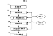
実施形態の情報記録媒体の製造方法においては、図5に示すように、スパッタ装置に基板を装填する工程S1と、金属窒化物を構成する金属からなる合金ターゲットを用いた反応スパッタ法により、記録層を形成する記録層形成工程S4を含み、この記録層形成工程におけるAr及びN2を含む雰囲気中で流量比Ar:N2が80:10〜10:80の範囲内に設定する。また、図5に示すように、反射層を設ける場合は、基板装填工程S1の後に、Arガス雰囲気として所定ターゲットを用いてスパッタ法により、反射層を形成す反射層形成工程S2及び第1誘電体層を形成する第1誘電体層形成工程S3と、記録層形成工程S4(Ar:N2雰囲気)と、第2誘電体層を形成する第2誘電体層形成工程S5(Ar雰囲気)と、の順序となる。最後に、カバー層を形成する(S6)。
Bi、Snのうちの1つ以上の元素とGe、Ti、Si、Alのうちのいずれかの元素との窒化物例えばGeBiNからなる記録層5は、405nm近傍での光の吸収率を未記録部で10%以上とすることが可能である。例えば385〜450nmの短波長域においてもこのような吸収率を得ることが可能なので、短波長レーザ光を用いる高密度記録にも対応することができる。記録層に金属窒化物を含有することで、青紫色レーザを用いた記録において、少ない記録エネルギーで記録を行うことができる。しかも、反応スパッタによって金属窒化物における窒素の比率を制御して記録層の吸収率を変更できるため、媒体設計の自由度が高くなり、高反射率と適度な記録感度とが共に得られ、同時に、高変調度、低ジッタ、低クロストークも実現可能である。
なお、スパッタ雰囲気中にAr以外のXe、Krなど不活性ガスを加えることもできる。また、ターゲットとして金属を用いるが、化学量論組成からはずれたものを用いてもよい。さらに、金属窒化物ターゲットを用いることにより、N2ガスを用いないでArのみ用い上記記録層を形成してもよい。
記録層の膜厚は記録層の物性、誘電体層の物性及びその厚さに応じて適宜決定するが、5〜40nm、好ましくは10〜30nm例えば12nmで十分なジッタが取れることを確認した。5nmより記録層が薄すぎると変調度を大きくすることが困難となり、40nmより厚すぎると記録層での光吸収のために反射率が不十分となる。
以下、図1に示す実施の形態について記録層5以外の構成を詳細に説明する。
[基板2]
基板2はガラス又はアクリル樹脂、ポリカーボネート樹脂、エポキシ樹脂若しくはポリオレフィン樹脂などのプラスチック樹脂が用いられる。また、平板上に紫外線硬化性樹脂などをスピンコート法などで、塗布硬化させたり、プラスチック樹脂のシートを接着剤で貼り合わせたものも用いられる。
基板2の寸法及び形状は特に限定されないが円盤状であり、その厚さは通常、0.3〜1.2mm程度である。基板2の表面には、トラッキング用やアドレス用など記録再生用光線を導くために、グルーブなどの所定のパターンが必要に応じて設けられ得る。記録再生光は、通常、グルーブ内に照射される。光入射側、光反射側のどちらかあるいは両方の基板にグルーブが設けられ得る。膜の積層は、光入射側、光反射側のどちらか側から行っても構わない。また、基板2をディスク以外の形状、例えばカード状の記録媒体としてもよい。
[誘電体層4、6]
誘電体層4、6は、各種誘電体から構成され特に限定されず、例えば、SiO2、SiNx、ZnSなどの酸化物、窒化物、硫化物、各種、金属酸化物、金属炭化物、の金属化合物及びその混合物例えばZnS−SiO2である。あるいは、La、Si、O及びNを含有するいわゆるLaSiON、Si、Al、O及びNを含有するいわゆるSiAlON誘電体については、従来から、PRTR法で指定されていない材料の組み合わせのみを選択することができる。誘電体層を複数の層で構成してもよい。
光入射側の第2誘電体層は厚さ0〜100nmで、光学的反射率調整用及び、記録モードをhigh to lowもしくはlow to highの所望の性能の方に調整するために設けられている。
光反射側の第1誘電体層は、レーザの光による熱が反射層に逃げる前に一時的に蓄熱して、記録層を十分に加熱する作用がある。誘電体層の厚さは40nm以下、好ましくは10〜30nmである。
[反射層3]
反射層3は、高反射率の金属や合金から構成することが好ましく、例えば、Ag、Al、Au、Pt、Cuなどの1種、又はこれらを少なくとも1種含む合金などから適宜選択すればよい。
反射層3の厚さは、30〜150nmとすることが好ましい。厚さが当該範囲未満であると十分な反射率が得にくくなる。また、当該範囲を超えても反射率の向上は小さく、コスト的に不利になる。反射層3は、スパッタ法や蒸着法などの気相成長法により形成することが好ましい。
また、反射層に半透過膜を用いることもできる。記録層構造が積層されている多層記録ディスクのピックアップから見て手前側の層の構造としても適用することができる。反射層無しの場合は、基板/誘電体層/記録層/誘電体層/カバー層の積層順序となる。
[光透過カバー層7]
情報記録媒体1では、光透過カバー層7を通して記録層5に記録光及び再生光が照射されるので、光透過カバー層7はこれらの光に対して実質的に透明である必要がある。また、光透過カバー層7は、耐擦傷性や耐食性の向上のために設けるものであり、種々の有機系の物質から構成することが好ましいが、特に、放射線硬化型化合物やその組成物を、電子線、紫外線などの放射線により硬化させた物質から構成することができる。
光透過カバー層7の厚さは、通常、0.1〜600μm程度であり、スピンコート、グラビア塗布、スプレーコート、ディッピングなど、通常の方法により形成すればよい。具体的には、アクリル樹脂、ポリカーボネート樹脂、エポキシ樹脂、ポリオレフィン樹脂などの各種樹脂を用いればよい。プラスチック樹脂のシートを接着剤で貼り合わせたものも用いられる。
[層構造]
以上では、本発明を片面記録型の情報記録媒体に適用する場合について説明したが、本発明は両面記録型の情報記録媒体にも適用可能である。また、片面記録型であって、光透過カバー層7上に保護層を接着した構成とすることもできる。このように記録媒体の層構造は、上記記録層の組成、組合せ以外でも、本発明の要件を満たせば、例えば、光透過カバー層が無い構成、誘電体層、記録層、反射層以外に、更に他の材料の層を追加した構成、記録層が更に多層である構成、反射層の無い構成、反射層が2層である構成、光反射側基板が無い構成、光入射側及び光反射側基板の位置に更に記録媒体構成が1つ以上追加されていて多層記録が可能なようにしてある構成、など、様々な構成に適用することが可能である。
以下、本発明の実施例を挙げ、実施例を詳細に説明する。
[実施例1]
基板2の表面に、反射層3、第1誘電体層4、記録層5、第2誘電体層6、及び光透過カバー層7を形成し、図1に示される構成の光ディスクのサンプルを作製した。
光反射側基板として、厚さ1.1mm、直径12cm、深さ27nmでピッチ0.320μmのスパイラル案内溝を設けたポリカーボネート樹脂の基板を使用した。
基板の上に、厚さ100nmのAg−Pd−Cu合金反射層、厚さ10nmのZnS−SiO2第1誘電体層をスパッタリング法によって順次成膜積層した。
その後、Bi−Geターゲットを用いて、Arガス80sccmに対してN2ガス10sccmの雰囲気中で反応スパッタリング法で厚さ12nmの記録層を成膜した。反応スパッタ時の条件は、例えば、RFマグネトロンスパッタ装置で、基板ターゲット間距離120mm、雰囲気圧力0.4〜0.8Pa、電力150Wである。
その後、更に厚さ40nmの光入射側ZnS−SiO2第2誘電体層をスパッタリング法によって成膜積層した。
その上に、光入射側保護層としてポリカーボネート樹脂シートを、カバー層の厚さが0.1mmになるように、紫外線硬化樹脂接着剤に用いて貼り合わせて、実施例の記録媒体を得た。
作製サンプルに、マルチパス記録を用いて、記録パワー5.3mW及びウィンドウ幅15.15nsecとし、線速度5.3m/sで、波長405nm光源を有する対物レンズ開口数0.85の光ヘッドを用いて、1−7変調のランダムパターンを記録した。記録後ジッタを測定したところ、約9.8%のジッタが得られた。
[実施例2]
Arガス70sccmに対してN2ガス20sccmの雰囲気中で反応スパッタして記録層を成膜し、厚さ25nmの光入射側ZnS−SiO2第2誘電体層を設けた以外、実施例1と同一にして、実施例2を形成した。
記録パワー5.0mWとした以外、実施例1と同一にしてランダムパターンを記録し、記録後ジッタを測定したところ、約7.5%の良好なジッタが得られた。
[実施例3]
Arガス50sccmに対してN2ガス40sccmの雰囲気中で反応スパッタして記録層を成膜し、厚さ20nmの光入射側ZnS−SiO2第2誘電体層を設けた以外、実施例1と同一にして、実施例3を形成した。
記録パワー5.2mWとした以外、実施例1と同一にしてランダムパターンを記録し、記録後ジッタを測定したところ、約7.3%の良好なジッタが得られた。
[実施例4]
Arガス20sccmに対してN2ガス70sccmの雰囲気中で反応スパッタして記録層を成膜し、厚さ15nmの光入射側ZnS−SiO2第2誘電体層を設けた以外、実施例1と同一にして、実施例4を形成した。
記録パワー5.7mWとした以外、実施例1と同一にしてランダムパターンを記録し、記録後ジッタを測定したところ、約7.4%の良好なジッタが得られた。
[比較例1]
窒素を添加せずArガスのみの雰囲気中でスパッタして厚さ25nmBiGe記録層を成膜し、厚さ20nm、40nmの光入射側及び反射側ZnS−SiO2誘電体層を設けた以外、実施例1と同一にして、比較例1を形成した。
記録パワー5.0mWとした以外、実施例1と同一にしてランダムパターンを記録し、記録後ジッタを測定したところ、20%以上の測定不可能なレベルであった。
[比較例2]
反射層を成膜せずに、さらに窒素を添加せずArガスのみの雰囲気中でスパッタして厚さ30nmBiGe記録層を成膜し、厚さ30nm、35nmの光入射側及び反射側ZnS−SiO2誘電体層を設けた以外、実施例1と同一にして、比較例2を形成した。
記録パワー5.0mWとした以外、実施例1と同一にしてランダムパターンを記録し、記録後ジッタを測定したところ、約16%のジッタが得られた。
[結果]
サンプルで得られた測定結果を、図6及び図7に実施例の記録層における波長405nm及び波長635nm光の吸収率変化(ZnS−SiO2誘電体層で封止した状態で測定)、図8に実施例の記録層における窒素添加量に関する記録パワー及び記録後ジッタ変化、図9に実施例の記録層における窒素添加量に関する成膜レート変化、それぞれ示す。
図6から、GeBi窒化物からなる記録層は、405nm近傍での光の吸収率を未記録部で10%以上を確保できることが分かる。
図7から、窒素を加えることで記録層の635nm近傍の吸収は大きく低下して記録感度が下がるので、記録再生に波長635nm光を用いる情報記録媒体では記録感度の制約によって窒素は微少量しか添加できないことが分かる。
図8から、反応スパッタにおける窒素添加は、好ましくは、記録層が十分な感度及び記録後ジッタ特性を持つだけ添加が必要(スパッタ雰囲気流量比Ar:N2=80:10〜0:100)で、かつ400nm近傍の青紫色レーザで十分な吸収を持つ範囲(スパッタ雰囲気流量比Ar:N2=30:60〜100:0)であることが分かる。
図9から、反応スパッタリングであるため窒素ガス導入量の増加とともに成膜レートが遅くなり、作製が簡単である必要性から成膜レートが2nm/min以上となる範囲がスパッタ雰囲気流量比Ar:N2=10:80〜100:0であることが分かる。
[さらなる実施例A〜C]
上記実施例と同様に、ポリカーボネート樹脂の基板上に、Ag合金反射層、ZnS−SiO2第1誘電体層、記録層、ZnS−SiO2第2誘電体層、の順に各層をスパッタ法及び反応スパッタ法によって積層した。記録層は窒化していない金属成分の合金ターゲットを用いてArガス中に窒素ガスを導入して反応スパッタを用いて成膜した。その後、ポリカーボネートシートを紫外線硬化樹脂を接着剤に用いて貼り合わせて硬化させて厚さ0.1mmの光入射側保護層を作成し、実施例A〜Cの光ディスクを製造した。表3は各層の膜厚、記録層(膜厚、組成、積層順)と反応スパッタ条件を示す。
上記比較例と同様に、窒素N2添加をせずに合金で記録層を成膜した以外、実施例と同一にして、比較例H、Iの光ディスクを製造した。表4は各層の膜厚、記録層(膜厚、組成、積層順)とスパッタ条件を示す。
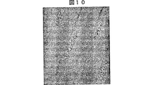
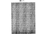
図10にBiGeN記録層(実施例2)の記録マークのTEM(transmission electron microscope)観察像を、図11にSnTiN記録層(ディスクA)の記録マークのTEM観察像を示す。どちらも記録案内溝からはみ出さずにサブマイクロ泡からなる良好な形状の記録マークが形成されていることが確認できる。さらに、図示しないが原子間力顕微鏡(AFM:atomic force microscope)観察像によると、溝深さ27nmの記録案内溝に対して、未記録部と記録部との膜厚方向の高低差はせいぜい6nm程度であった。
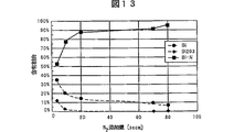
実施例光ディスクのBiGeN記録層におけるGe及びBi並びにそれらの窒化物及び酸化物をESCA分析し、その測定結果を、表6に示す。表6に基づき、図12は窒素添加量に関する非窒化物(Ge、酸化物)及び窒化物の含有割合の変化を、図13は窒素添加量に関する非窒化物(Bi、酸化物)及び窒化物の含有割合の変化を示す。
つまり、窒素導入量10sccm以上で記録層中のGeが85%以上に窒化していることが分かる。窒素導入量の多い方では、成膜レートが下がってくるので、窒素導入量は10〜80sccmで有効である。好ましくは記録層の吸収が十分にある範囲の方が記録感度の点で優位であるので、窒素導入量は10〜60sccmが望ましい。
同様に、成膜時の窒素導入量5sccmでは金属Biが残っている。記録層中にBiは金属BiとBi−N組成の混合体で存在し、成膜時の窒素導入量が増える程、窒化物の割合が増える。
成膜時の窒素導入量80sccmではBiの約94%が窒化されている。よって、Geが85%以上に窒化していて、Biが94%以下窒化されていることが好ましい。さらに、Geが85%以上に窒化していて、記録感度を高めるための成膜時の窒素導入量60sccmの場合ではBiが90%以下窒化されていることが好ましい。
したがって、記録層中の金属成分比率は広範囲(金属窒化物などの高温分解化合物が20〜40atm.%の範囲)で良好な特性が得られるが、高温分解化合物を窒化物で形成するには、成膜時に完全に窒化するように窒素流量を調整する必要がある。
窒素導入流量比率を上げると低温分解窒化物の非窒化成分が減少して吸収が減って記録層の感度が悪くなるとともに、成膜レートが下がり生産性が低下するので、窒素導入量はできるだけ少なめに調整した方が生産性の面では有利である。
高温分解化合物を金属窒化物とした時の記録層を成膜する反応性スパッタリングの成膜条件設定方法は、図14に示すように、まず、金属窒化物の金属成分の合金、その酸化物及びその窒化物の少なくとも1つからなるスパッタリングターゲット、例えば記録層用合金ターゲットの作製し(SS1)、初期値からスパッタリング導入ガスのArガスと窒素ガスの流量決定し(SS2)、反応スパッタリング成膜し(SS3)、成膜された記録層の成分分析し(SS4)、高温分解化合物が完全に窒化しているか否かを判断する(SS5)。ここで、高温分解化合物が完全に窒化されていない場合は窒素ガスの流量決定工程へ戻り窒素ガスの流量を増加し、窒化を完了させる。一方、高温分解化合物が完全に窒化されている場合は、低温分解窒化物の非窒化成分が十分にあるか否かを判断する(SS6)。ここで、低温分解窒化物の非窒化成分が十分にない場合は窒素ガスの流量決定工程へ戻り窒素ガスの流量を減少し、非窒化成分を記録層中に確保する。一方、非窒化成分が記録層中に十分ある場合は、その状態の窒素ガスの流量を決定値とすることで記録層の成膜条件設定が完了し(SS7)、記録層作製工程へ進む。また、金属窒化物以外を使用する時にも同様な方法で成膜条件を設定すれば良い。
図15に記録層を成膜するためのスパッタリングターゲットの、バッキングプレートPPに固定された円盤状のターゲットTを示す概略断面図を示す。ターゲットは一様な合金又は窒化物又は酸化物として形成してもよく、あるいは、スパッタ率を考慮して単体のモザイクとしても構成できる。
本発明によれば、記録パワーによって分解し易い金属窒化物と分解しにくい金属化合物の混合膜とすることで、熱分解反応を制御して、最低限の形状変化で図10及び図11のように微細マークを形良く形成し、主として熱分解後の記録層の光学特性の変化によって記録を行うことができる。こうして記録前後の反射率の差が大きくS/N比が高く、ジッタ特性が優れた記録層が得られる。
また、その混合膜をスパッタリングターゲットを調整することで窒素導入反応性スパッタによって一度に形成できる。
更に、記録層に環境基準で毒物指定されていない無機材料が選択可能である。
【図面の簡単な説明】
図1は、本発明の情報記録媒体を示す概略部分断面図である。
図2は、本発明の情報記録媒体を示す概略部分平面図である。
図3は、情報記録媒体のBiN記録層の示差走査熱分析曲線を示すグラフである。
図4は、情報記録媒体のBiN記録層の記録前後のESCA分析のスペクトル特性を示すグラフである。
図5は、本発明の情報記録媒体製造方法を示すフローチャートである。
図6は、実施例の記録層における波長405nm光の吸収率変化を示すグラフである。
図7は、実施例の記録層における波長635nm光の吸収率変化を示すグラフである。
図8は、実施例の記録層における窒素添加量に関する記録パワー及び記録後ジッタ変化を示すグラフである。
図9は、実施例の記録層における窒素添加量に関する成膜レート変化を示すグラフである。
図10は、実施例のBiGeN記録層の記録マークのTEM写真である。
図11は、実施例のSnTiN記録層の記録マークのTEM写真である。
図12は、実施例の記録層における窒素添加量に関するGe、その窒化物及び酸化物の含有割合の変化を示すグラフである。
図13は、実施例の記録層における窒素添加量に関するBi、その窒化物及び酸化物の含有割合の変化を示すグラフである。
図14は、実施例の記録層を成膜する反応性スパッタリングの成膜条件設定方法を示すフローチャートである。
図15は、実施例の記録層を成膜するためのスパッタリングターゲットを示す概略断面図である。
図16は、従来の情報記録媒体を示す概略部分平面図である。 Technical field
The present invention relates to an optical information recording medium such as an optical disk or an optical card for recording / reproducing information by irradiation with a light beam, and a method for manufacturing the same.
Background art
In recent years, a DVD (Digital Versatile Disc) has been widely used as an information recording medium for recording and reproducing data such as video data, audio data, and computer data. In addition to reproduction, this DVD can be additionally recorded using an organic dye material in the recording layer (DVD-R (recordable)), or a DVD-RW (rewritable using a phase change material as the recording layer). re-recordable).
There is a demand for recording and reproduction with a light beam having a wavelength shorter than 635 nm in the further increase in density, but sufficient optical disk characteristics cannot be realized in a conventional write once optical disk.
In addition, as a write-once optical disk, a hole is formed in the recording layer by laser light irradiation, a balloon-like cavity is created in the recording layer to raise the film, or a substance that disperses the pyrolysis product in the recording layer is added. What to do has been reported. In these conventional recording methods, there is a problem that it is difficult to control the size and edge of the mark in forming a fine recording mark as the density increases. That is, as shown in FIG. 16, recording is performed with deformation as a large mark protruding from the recording guide groove.
The write-once optical disc cannot be rewritten to the part once recorded, so that the amount of consumption increases, and it is necessary to consider the environmental impact at the time of disposal. This is because there is a case where a material that is harmful in the law (PRTR law) concerning promotion of improvement such as grasping and managing the discharge amount of a specific chemical substance to the environment is added.
Disclosure of the invention
An object of the present invention is to provide an information recording medium having a large difference in reflectance before and after recording and excellent characteristics such as jitter characteristics and a method for manufacturing the same.
The information recording medium of the present invention is an information recording medium comprising a recording layer made of a material whose reflectivity is changed by irradiation of a light beam and information recorded as a change in reflectivity and a substrate carrying the recording layer. The recording layer is made of a metal nitride.
The recording layer of the information recording medium of the present invention comprises a low-temperature decomposition nitride that decomposes below a predetermined temperature to generate nitrogen and is not completely nitrided, and a high-temperature decomposition compound that decomposes at a temperature exceeding the predetermined temperature. It consists of a mixture.
The method for producing an information recording medium of the present invention comprises a recording layer made of a material whose reflectance changes upon irradiation with a light beam, information recorded as a change in reflectance, and a substrate carrying the recording layer, A manufacturing method for manufacturing an information recording medium in which a recording layer is made of a metal nitride, comprising a recording layer forming step of forming the recording layer by a reactive sputtering method using a target made of a metal constituting the metal nitride. Ar and N in the recording layer forming step2Flow ratio Ar: N in an atmosphere containing2Is set within the range of 80:10 to 10:80.
BEST MODE FOR CARRYING OUT THE INVENTION
Embodiments of the present invention will be described with reference to the drawings.
FIG. 1 shows a configuration example of the embodiment. This
The
In addition, the
[Recording principle]
The recording layer of the recording medium is a recording layer mainly composed of a metal compound such as a uniformly dispersed alloy and a nitride thereof. During recording, a reaction occurs in which nitrogen is released from the nitride in the recording layer by irradiation with laser light. For this purpose, since the recording layer needs to absorb the laser beam, the nitride must have an absorptance. Therefore, the nitride needs to contain a certain amount of non-nitrided components, not nitrided over the entire surface and having a high transmittance. However, in the case of a recording layer containing only insufficient nitride, the film quality is close to that of an amorphous metal thin film, so that the rigidity and stress of the film are low and the thermal conductivity is high. Therefore, since the heat spreads in the lateral direction during heating, the temperature of the film is difficult to rise, and the thermal decomposition of nitrogen spreads in a chain reaction, for example, a phenomenon such as mark recording that is larger than the light spot as shown in FIG. turn into. This is not so much a problem if the size of the recording mark is about CD, but it is difficult to control the mark edge when forming a fine mark having a width of 0.1 to 0.2 μm by irradiation with blue-violet laser light. Problems arise.
Therefore, the recording layer is made of a mixed film composed of a highly rigid substance that is difficult to pyrolyze and a nitride that is easily pyrolyzed, thereby controlling the pyrolysis reaction to form fine marks in a good shape. In addition, since recording is performed based on the amount of change in optical characteristics, a substance that has a high transmittance with respect to reading light is selected as a substance that is difficult to thermally decompose. Specifically, the recording layer includes a low-temperature decomposition nitride (nitrogen releasing material), a non-nitride (non-nitriding component of nitride = heat absorber), and a high-temperature decomposition compound (metal nitride, metal oxide, or metal carbide). Or a mixture thereof = a thermal decomposition reaction controlling substance). Actually, the recording layer composition can be realized by using the non-nitride as a non-nitriding component in the nitride. Therefore, the recording layer of the recording medium is composed of two kinds of mixtures of a low temperature decomposition nitride having a non-nitriding component and a high temperature decomposition compound.
The recording principle of a disc using this recording layer system is considered as follows.
First, the recording laser beam is absorbed by the heat absorber, and the temperature rises. Next, the low temperature decomposition nitride decomposes and releases nitrogen. Next, (1) the optical characteristics of the recording layer change due to the release of nitrogen. Next, (2) the recording layer is deformed by the released nitrogen. Here, (2) is a secondary recording mode. Although the recording layer is not mainly deformed, if the recording layer is pressed with a strong pressure so as not to be deformed at all, the separation of nitrogen may be hindered. Therefore, it is better to make some deformation. The dielectric layer plays a role of receiving the deformation of the recording layer when nitrogen is released from the recording layer and has a heat insulating effect on the adjustment of optical characteristics and the heat dissipation action of the metal reflecting layer. Of these, the reflective layer is provided for the purpose of securing the heat radiation characteristics and the signal amount due to multiple reflection, and thus may not necessarily be provided.
In an optical disk, the temperature of a recording layer that rises by irradiation with a recording laser beam is estimated to be 400 to 600 ° C. at the maximum. Therefore, it is necessary to select the low-temperature decomposition nitride and the high-temperature decomposition compound based on the decomposition temperature with a threshold of about 600 ° C. Table 1 shows the approximate decomposition temperatures of various metal nitrides.
The low-temperature decomposed nitride needs to exhibit a reaction in which nitrogen is separated at a low temperature of 600 ° C. or lower, and further, a reaction at 400 ° C. or lower is desirable from the viewpoint of recording sensitivity. However, if the reaction is carried out at a very low temperature, there is a concern about the effect on storage characteristics, and therefore a substance that reacts at 80 ° C. or lower cannot be selected. Therefore, 100 degreeC or more is preferable. In addition, consideration should be given to materials that are designated by the PRTR method as environmental considerations. As a result of examination including the condition that the material can be formed by sputtering, we focus on Bi and Sn nitrides, which are low melting point metals, as candidates for low-temperature decomposition nitrides. If the PRTR method is not taken into account, a material such as Cu can be used.
When a BiN film (recording layer) was prepared and differential scanning calorimetry was performed, it was confirmed that it decomposed at about 220 ° C. as shown in FIG. Further, the actual reaction start temperature is about 180 ° C., and it is considered that the decomposition reaction starts from a temperature lower by 50 to 70 ° C. than the decomposition temperature, and from a temperature lower by 50 to 100 ° C. in view of errors and margins. An optical disc having a recording layer in which BiN and SnN are low-temperature decomposition nitrides was prepared and evaluated. As a result, it was concluded that BiN is superior to SnN as a low-temperature decomposition nitride. However, there is no big problem even if SnN is selected.
FIG. 4 shows, as an example, spectral characteristics of ESCA (Electron Spectroscopy for Chemical Analysis), that is, X-ray electron spectroscopy analysis before and after recording when BiN is used as a low-temperature decomposition nitride in the recording layer. In the spectral characteristics, a peak of metal Bi, which was hardly present in the unrecorded portion, appeared after recording, and it was confirmed that the decomposition of nitrogen and bismuth occurred by recording.
[High-temperature decomposition compound]
The high-temperature decomposition compound is stable without being decomposed at a temperature of 600 ° C. or less, and needs to be a film having a relatively high transmittance for reading light and a high hardness. Typical metal compounds include metal nitrides, metal oxides, metal carbides, and the like, and mixtures thereof may be used. In addition, as a consideration for the environment, the material is selected under the condition that it is a material that can be sputter-deposited simultaneously with the low-temperature decomposition nitride except for materials specified by the PRTR method. GeN, SiN, AlN, and TiN are preferred as metal nitrides that are stable at high temperatures.
GeN, SiN, AlN, and TiN were subjected to differential scanning calorimetry, and it was confirmed that GeN did not decompose by 500 ° C. As a result of examining the recording layer using these nitrides as a high-temperature decomposition compound by actually forming a disk, good results were obtained in the order of GeN> TiN> SiN> AlN. It is preferable in terms of characteristics to use GeN or TiN. Besides nitrides, metal compounds that are stable at high temperatures include SiO2, Al2O3, GeO2, SnO, Bi2O3It is also possible to select a stable metal oxide such as SiC, a stable metal carbide such as SiC, or a mixture thereof. Many oxides have strong thermal stability, and some have a glass transition at high temperatures. Of the carbides, SiC has a high thermal stability and cannot be melted under atmospheric pressure.
Table 2 shows the melting points instead of the decomposition temperatures of oxides and carbides. The melting point is indicated that the decomposition temperature is higher. In addition, the sublimation point lower than the melting point showed the sublimation point.
The metal
In the information recording medium manufacturing method of the embodiment, as shown in FIG. 5, recording is performed by the step S1 of loading a substrate into a sputtering apparatus and the reactive sputtering method using an alloy target made of metal constituting a metal nitride. Recording layer forming step S4 for forming a layer, and Ar and N in this recording layer forming step2Flow ratio Ar: N in an atmosphere containing2Is set within the range of 80:10 to 10:80. Further, as shown in FIG. 5, when the reflective layer is provided, the reflective layer forming step S2 for forming the reflective layer by sputtering using a predetermined target as an Ar gas atmosphere and the first dielectric after the substrate loading step S1. A first dielectric layer forming step S3 for forming a body layer, and a recording layer forming step S4 (Ar: N2Atmosphere) and the second dielectric layer forming step S5 (Ar atmosphere) for forming the second dielectric layer. Finally, a cover layer is formed (S6).
A
An inert gas such as Xe or Kr other than Ar can be added to the sputtering atmosphere. Moreover, although a metal is used as the target, a material deviating from the stoichiometric composition may be used. Furthermore, by using a metal nitride target, N2The recording layer may be formed using only Ar without using a gas.
The thickness of the recording layer is appropriately determined according to the physical properties of the recording layer, the physical properties of the dielectric layer, and the thickness thereof, but it was confirmed that sufficient jitter can be obtained at 5 to 40 nm, preferably 10 to 30 nm, for example, 12 nm. If the recording layer is thinner than 5 nm, it is difficult to increase the degree of modulation. If it is thicker than 40 nm, the reflectance is insufficient due to light absorption by the recording layer.
Hereinafter, the configuration other than the
[Substrate 2]
The
Although the dimension and shape of the board |
[
The
The second dielectric layer on the light incident side has a thickness of 0 to 100 nm, and is provided for adjusting the optical reflectivity and adjusting the recording mode to a desired performance of high to low or low to high. .
The first dielectric layer on the light reflecting side has an effect of sufficiently storing the recording layer by temporarily storing heat before the heat from the laser light escapes to the reflecting layer. The thickness of the dielectric layer is 40 nm or less, preferably 10 to 30 nm.
[Reflection layer 3]
The
The thickness of the
A semi-transmissive film can also be used for the reflective layer. The present invention can also be applied as a layer structure on the near side when viewed from the pickup of a multilayer recording disk in which the recording layer structure is laminated. When there is no reflective layer, the stacking order is substrate / dielectric layer / recording layer / dielectric layer / cover layer.
[Light transmission cover layer 7]
In the
The thickness of the light transmission cover layer 7 is usually about 0.1 to 600 μm, and may be formed by a usual method such as spin coating, gravure coating, spray coating, dipping or the like. Specifically, various resins such as an acrylic resin, a polycarbonate resin, an epoxy resin, and a polyolefin resin may be used. A plastic resin sheet bonded with an adhesive may also be used.
[Layer structure]
The case where the present invention is applied to a single-sided recording type information recording medium has been described above, but the present invention is also applicable to a double-sided recording type information recording medium. Further, it may be a single-sided recording type in which a protective layer is adhered on the light transmission cover layer 7. Thus, the layer structure of the recording medium, other than the composition and combination of the recording layers, satisfies the requirements of the present invention, for example, a configuration without a light-transmitting cover layer, a dielectric layer, a recording layer, and a reflective layer, A configuration in which layers of other materials are added, a configuration in which the recording layer is further multi-layered, a configuration in which there is no reflective layer, a configuration in which there are two reflective layers, a configuration in which there is no light reflecting side substrate, a light incident side and a light reflecting side The present invention can be applied to various configurations such as a configuration in which one or more recording medium configurations are further added at the substrate position so that multi-layer recording is possible.
Hereinafter, examples of the present invention will be given and described in detail.
[Example 1]
A
As the light reflecting substrate, a polycarbonate resin substrate having a thickness of 1.1 mm, a diameter of 12 cm, a depth of 27 nm and a spiral guide groove with a pitch of 0.320 μm was used.
On the substrate, an Ag—Pd—Cu alloy reflective layer with a thickness of 100 nm, a ZnS—SiO with a thickness of 10 nm.2The first dielectric layer was sequentially deposited by sputtering.
After that, using a Bi-Ge target, N gas against Ar gas at 80 sccm.2A recording layer having a thickness of 12 nm was formed by reactive sputtering in an atmosphere of 10 sccm of gas. The conditions for the reactive sputtering are, for example, an RF magnetron sputtering apparatus, a distance between substrate targets of 120 mm, an atmospheric pressure of 0.4 to 0.8 Pa, and a power of 150 W.
After that, the light incident side ZnS-SiO having a thickness of 40 nm2A second dielectric layer was deposited and deposited by sputtering.
On top of that, a polycarbonate resin sheet as a light incident side protective layer was bonded using an ultraviolet curable resin adhesive so that the thickness of the cover layer was 0.1 mm to obtain the recording medium of the example.
An optical head having a numerical aperture of 0.85 having a light source with a wavelength of 405 nm, a linear velocity of 5.3 m / s, a recording power of 5.3 mW and a window width of 15.15 nsec is used as a production sample. Thus, a random pattern of 1-7 modulation was recorded. When jitter was measured after recording, a jitter of about 9.8% was obtained.
[Example 2]
N for 70 sccm of Ar gas2A recording layer is formed by reactive sputtering in an atmosphere with a gas of 20 sccm, and a light incident side ZnS-SiO having a thickness of 25 nm is formed.2Example 2 was formed in the same manner as Example 1 except that the second dielectric layer was provided.
A random pattern was recorded in the same manner as in Example 1 except that the recording power was 5.0 mW, and the jitter after recording was measured. As a result, a good jitter of about 7.5% was obtained.
[Example 3]
N for Ar gas 50sccm2A recording layer is formed by reactive sputtering in an atmosphere of 40 sccm of gas, and the light incident side ZnS-SiO having a thickness of 20 nm is formed.2Example 3 was formed in the same manner as Example 1 except that the second dielectric layer was provided.
A random pattern was recorded in the same manner as in Example 1 except that the recording power was set to 5.2 mW, and the jitter after measurement was measured. As a result, a good jitter of about 7.3% was obtained.
[Example 4]
N for 20 sccm of Ar gas2A recording layer is formed by reactive sputtering in an atmosphere with a gas of 70 sccm, and the light incident side ZnS-SiO having a thickness of 15 nm is formed.2Example 4 was formed in the same manner as Example 1 except that the second dielectric layer was provided.
A random pattern was recorded in the same manner as in Example 1 except that the recording power was 5.7 mW, and the jitter after recording was measured. As a result, a good jitter of about 7.4% was obtained.
[Comparative Example 1]
Sputtering was performed in an atmosphere containing only Ar gas without adding nitrogen, and a 25 nm-thick BiGe recording layer was formed, and a light incident side and a reflection side ZnS-SiO having a thickness of 20 nm and 40 nm were formed.2Comparative Example 1 was formed in the same manner as Example 1 except that a dielectric layer was provided.
A random pattern was recorded in the same manner as in Example 1 except that the recording power was 5.0 mW, and the jitter was measured after recording.
[Comparative Example 2]
Sputtering was performed in an Ar gas-only atmosphere without forming a reflective layer and further adding nitrogen, and a 30 nm-thick BiGe recording layer was formed, and light incident side and reflective side ZnS-SiO having a thickness of 30 nm and 35 nm were formed.2Comparative Example 2 was formed in the same manner as Example 1 except that a dielectric layer was provided.
A random pattern was recorded in the same manner as in Example 1 except that the recording power was 5.0 mW, and the jitter after recording was measured. As a result, a jitter of about 16% was obtained.
[result]
The measurement results obtained for the samples are shown in FIG. 6 and FIG.2FIG. 8 shows changes in recording power and post-recording jitter in the recording layer of the example, and FIG. 9 shows changes in film forming rate in relation to the amount of nitrogen in the recording layer of the example. , Respectively.
FIG. 6 shows that the recording layer made of GeBi nitride can secure 10% or more of the light absorptance in the vicinity of 405 nm in the unrecorded portion.
From FIG. 7, by adding nitrogen, the absorption in the vicinity of 635 nm of the recording layer is greatly reduced and the recording sensitivity is lowered. Therefore, in an information recording medium using a wavelength of 635 nm for recording and reproduction, only a small amount of nitrogen is added due to the limitation of recording sensitivity. I understand that I can't.
From FIG. 8, it is preferable to add nitrogen in the reactive sputtering as long as the recording layer has sufficient sensitivity and post-recording jitter characteristics (sputtering atmosphere flow ratio Ar: N2= 80: 10 to 0: 100) and a range where the blue-violet laser near 400 nm has sufficient absorption (sputtering atmosphere flow ratio Ar: N2= 30: 60 to 100: 0).
From FIG. 9, since the reactive sputtering is used, the film formation rate is slowed with an increase in the amount of nitrogen gas introduced, and the range in which the film formation rate is 2 nm / min or more is necessary due to the need for simple production.2It can be seen that = 10: 80 to 100: 0.
[Further Examples A to C]
Similar to the above example, on the polycarbonate resin substrate, an Ag alloy reflective layer, ZnS-SiO2First dielectric layer, recording layer, ZnS-SiO2Each layer was laminated in the order of the second dielectric layer by sputtering and reactive sputtering. The recording layer was formed using reactive sputtering by introducing nitrogen gas into Ar gas using a non-nitrided metal component alloy target. Thereafter, the polycarbonate sheet was bonded and cured using an ultraviolet curable resin as an adhesive to form a light incident side protective layer having a thickness of 0.1 mm, and optical disks of Examples A to C were manufactured. Table 3 shows the film thickness of each layer, the recording layer (film thickness, composition, stacking order) and reaction sputtering conditions.
Similar to the above comparative example, nitrogen N2Optical discs of Comparative Examples H and I were manufactured in the same manner as in Example except that the recording layer was formed of an alloy without addition. Table 4 shows the film thickness of each layer, the recording layer (film thickness, composition, stacking order) and sputtering conditions.
FIG. 10 shows a TEM (transmission electron microscope) observation image of the recording mark of the BiGeN recording layer (Example 2), and FIG. 11 shows a TEM observation image of the recording mark of the SnTiN recording layer (disc A). In either case, it can be confirmed that a recording mark having a good shape made of sub-micro bubbles is formed without protruding from the recording guide groove. Furthermore, although not shown, according to an atomic force microscope (AFM) observation image, the height difference in the film thickness direction between the unrecorded portion and the recorded portion is at most 6 nm with respect to the recording guide groove having a groove depth of 27 nm. It was about.
Example 6 Ge and Bi and their nitrides and oxides in the BiGeN recording layer of the optical disc were subjected to ESCA analysis, and the measurement results are shown in Table 6. Based on Table 6, FIG. 12 shows changes in the content ratio of non-nitride (Ge, oxide) and nitride with respect to the amount of nitrogen added, and FIG. 13 shows non-nitride (Bi, oxide) and nitride with respect to the amount of nitrogen added. The change of the content rate of is shown.
That is, it can be seen that Ge in the recording layer is nitrided to 85% or more when the nitrogen introduction amount is 10 sccm or more. In the case where the amount of nitrogen introduced is large, the film formation rate decreases, so the amount of nitrogen introduced is effective at 10 to 80 sccm. Preferably, the range in which the recording layer has sufficient absorption is superior in terms of recording sensitivity, and therefore, the nitrogen introduction amount is desirably 10 to 60 sccm.
Similarly, metal Bi remains when the amount of nitrogen introduced during film formation is 5 sccm. Bi exists in the recording layer as a mixture of metal Bi and Bi—N composition, and the nitride ratio increases as the amount of nitrogen introduced during film formation increases.
When the amount of nitrogen introduced during film formation is 80 sccm, about 94% of Bi is nitrided. Therefore, it is preferable that Ge is nitrided to 85% or more and Bi is 94% or less. Further, when Ge is nitrided to 85% or more, and Bi is introduced at a rate of 60 sccm during film formation for improving recording sensitivity, Bi is preferably nitrided 90% or less.
Therefore, good characteristics can be obtained in a wide range of the metal component ratio in the recording layer (the range of 20 to 40 atm.% Of the high-temperature decomposition compound such as metal nitride). To form the high-temperature decomposition compound with nitride, It is necessary to adjust the nitrogen flow rate so that nitriding is complete during film formation.
Increasing the nitrogen flow rate ratio reduces the non-nitriding component of the low-temperature decomposition nitride and reduces the absorption, which lowers the sensitivity of the recording layer and lowers the film formation rate and decreases the productivity. It is more advantageous in terms of productivity to adjust to.
As shown in FIG. 14, the reactive sputtering film forming condition setting method for forming the recording layer when the high temperature decomposition compound is a metal nitride is as follows. First, as shown in FIG. A sputtering target made of at least one of the nitrides, for example, an alloy target for a recording layer, is prepared (SS1), the flow rates of Ar gas and nitrogen gas as sputtering introduction gases are determined from the initial values (SS2), and reactive sputtering film formation is performed. (SS3), component analysis of the formed recording layer is performed (SS4), and it is determined whether the high temperature decomposition compound is completely nitrided (SS5). Here, when the high-temperature decomposition compound is not completely nitrided, the process returns to the nitrogen gas flow rate determination step to increase the flow rate of nitrogen gas to complete nitriding. On the other hand, when the high temperature decomposition compound is completely nitrided, it is determined whether or not the non-nitriding component of the low temperature decomposition nitride is sufficient (SS6). Here, when the non-nitriding component of the low-temperature decomposition nitride is not sufficient, the flow returns to the nitrogen gas flow determination step to reduce the flow rate of the nitrogen gas and ensure the non-nitriding component in the recording layer. On the other hand, when the non-nitriding component is sufficient in the recording layer, setting the flow rate of the nitrogen gas in that state as a determined value completes the setting of the recording layer deposition conditions (SS7), and proceeds to the recording layer manufacturing step. In addition, when using a material other than metal nitride, the film forming conditions may be set in the same manner.
FIG. 15 is a schematic cross-sectional view showing a disk-shaped target T fixed to a backing plate PP, which is a sputtering target for forming a recording layer. The target may be formed as a uniform alloy, nitride, or oxide, or may be configured as a single mosaic in consideration of the sputtering rate.
According to the present invention, by using a mixed film of a metal nitride that is easily decomposed by a recording power and a metal compound that is not easily decomposed, the thermal decomposition reaction is controlled, and as shown in FIGS. Fine marks can be formed in good shape, and recording can be performed mainly by changes in the optical characteristics of the recording layer after pyrolysis. Thus, a recording layer having a large difference in reflectance before and after recording and a high S / N ratio and excellent jitter characteristics can be obtained.
Moreover, the mixed film can be formed at a time by reactive sputtering with nitrogen introduction by adjusting the sputtering target.
Furthermore, an inorganic material that is not designated as a poison by the environmental standard can be selected for the recording layer.
[Brief description of the drawings]
FIG. 1 is a schematic partial sectional view showing an information recording medium of the present invention.
FIG. 2 is a schematic partial plan view showing the information recording medium of the present invention.
FIG. 3 is a graph showing a differential scanning calorimetry curve of the BiN recording layer of the information recording medium.
FIG. 4 is a graph showing spectral characteristics of ESCA analysis before and after recording on the BiN recording layer of the information recording medium.
FIG. 5 is a flowchart showing the information recording medium manufacturing method of the present invention.
FIG. 6 is a graph showing a change in absorptance of light having a wavelength of 405 nm in the recording layer of the example.
FIG. 7 is a graph showing a change in absorptance of light having a wavelength of 635 nm in the recording layer of the example.
FIG. 8 is a graph showing the recording power and the jitter change after recording with respect to the amount of nitrogen added in the recording layer of the example.
FIG. 9 is a graph showing changes in the film formation rate with respect to the amount of nitrogen added in the recording layer of the example.
FIG. 10 is a TEM photograph of the recording marks of the BiGeN recording layer of the example.
FIG. 11 is a TEM photograph of the recording marks of the SnTiN recording layer of the example.
FIG. 12 is a graph showing changes in the content ratios of Ge, nitrides thereof, and oxides with respect to the amount of nitrogen added in the recording layer of the example.
FIG. 13 is a graph showing changes in the content ratios of Bi, nitrides thereof, and oxides with respect to the amount of nitrogen added in the recording layer of the example.
FIG. 14 is a flowchart showing a reactive sputtering deposition condition setting method for depositing the recording layer of the example.
FIG. 15 is a schematic cross-sectional view showing a sputtering target for forming the recording layer of the example.
FIG. 16 is a schematic partial plan view showing a conventional information recording medium.
Claims (13)
Applications Claiming Priority (5)
| Application Number | Priority Date | Filing Date | Title |
|---|---|---|---|
| JP2002162047 | 2002-06-03 | ||
| JP2002162047 | 2002-06-03 | ||
| JP2003024139 | 2003-01-31 | ||
| JP2003024139 | 2003-01-31 | ||
| PCT/JP2003/006439 WO2003101750A1 (en) | 2002-06-03 | 2003-05-23 | Information recording medium and process for producing the same |
Related Child Applications (2)
| Application Number | Title | Priority Date | Filing Date |
|---|---|---|---|
| JP2006024611A Division JP3889028B2 (en) | 2002-06-03 | 2006-02-01 | Information recording medium |
| JP2006024612A Division JP2006182030A (en) | 2002-06-03 | 2006-02-01 | Information recording medium |
Publications (2)
| Publication Number | Publication Date |
|---|---|
| JPWO2003101750A1 JPWO2003101750A1 (en) | 2005-09-29 |
| JP3810076B2 true JP3810076B2 (en) | 2006-08-16 |
Family
ID=29714331
Family Applications (1)
| Application Number | Title | Priority Date | Filing Date |
|---|---|---|---|
| JP2004509072A Expired - Lifetime JP3810076B2 (en) | 2002-06-03 | 2003-05-23 | Information recording medium |
Country Status (10)
| Country | Link |
|---|---|
| US (1) | US7524612B2 (en) |
| EP (1) | EP1510355B1 (en) |
| JP (1) | JP3810076B2 (en) |
| KR (1) | KR100709931B1 (en) |
| CN (2) | CN1659041A (en) |
| AU (1) | AU2003242414A1 (en) |
| DE (1) | DE60311804T2 (en) |
| HK (1) | HK1072037A1 (en) |
| TW (1) | TWI236674B (en) |
| WO (1) | WO2003101750A1 (en) |
Cited By (1)
| Publication number | Priority date | Publication date | Assignee | Title |
|---|---|---|---|---|
| US8124211B2 (en) | 2007-03-28 | 2012-02-28 | Ricoh Company, Ltd. | Optical recording medium, sputtering target, and method for manufacturing the same |
Families Citing this family (21)
| Publication number | Priority date | Publication date | Assignee | Title |
|---|---|---|---|---|
| JP2005044450A (en) * | 2003-07-24 | 2005-02-17 | Tdk Corp | Optical recording medium and method for manufacturing same, and data recording method and data reproducing method for optical recording medium |
| CN1839052B (en) * | 2003-08-21 | 2011-09-07 | 三菱化学媒体股份有限公司 | Recording medium |
| US7952984B2 (en) | 2004-04-22 | 2011-05-31 | Tdk Corporation | Optical recording medium and method of recording and reproducing of optical recording medium |
| JP2006281751A (en) * | 2004-04-28 | 2006-10-19 | Sony Corp | Write-once optical recording medium |
| US7427431B2 (en) * | 2004-04-28 | 2008-09-23 | Sony Corporation | Write once optical recording medium |
| US7235501B2 (en) | 2004-12-13 | 2007-06-26 | Micron Technology, Inc. | Lanthanum hafnium oxide dielectrics |
| JP2006018986A (en) * | 2005-01-20 | 2006-01-19 | Pioneer Electronic Corp | Optical recording medium and its manufacturing method |
| JP4527766B2 (en) * | 2005-02-23 | 2010-08-18 | パイオニア株式会社 | Optical recording medium |
| US7972974B2 (en) | 2006-01-10 | 2011-07-05 | Micron Technology, Inc. | Gallium lanthanide oxide films |
| JP4560495B2 (en) * | 2006-06-16 | 2010-10-13 | 三菱化学メディア株式会社 | recoding media |
| US7544604B2 (en) | 2006-08-31 | 2009-06-09 | Micron Technology, Inc. | Tantalum lanthanide oxynitride films |
| US7759747B2 (en) | 2006-08-31 | 2010-07-20 | Micron Technology, Inc. | Tantalum aluminum oxynitride high-κ dielectric |
| US7563730B2 (en) | 2006-08-31 | 2009-07-21 | Micron Technology, Inc. | Hafnium lanthanide oxynitride films |
| US7776765B2 (en) | 2006-08-31 | 2010-08-17 | Micron Technology, Inc. | Tantalum silicon oxynitride high-k dielectrics and metal gates |
| US7605030B2 (en) | 2006-08-31 | 2009-10-20 | Micron Technology, Inc. | Hafnium tantalum oxynitride high-k dielectric and metal gates |
| JP4577581B2 (en) * | 2007-08-30 | 2010-11-10 | ソニー株式会社 | Optical information recording medium |
| JP2009143184A (en) * | 2007-12-17 | 2009-07-02 | Kobe Steel Ltd | Recording layer for optical information recording medium and optical information recording medium |
| WO2009104239A1 (en) * | 2008-02-18 | 2009-08-27 | 株式会社 東芝 | Non-volatile storage device and its manufacturing method |
| JP4969624B2 (en) | 2008-11-12 | 2012-07-04 | 株式会社神戸製鋼所 | Optical information recording medium |
| CN105931654B (en) | 2009-09-18 | 2019-07-02 | 株式会社神户制钢所 | Optical information recording medium recording layer, optical information recording medium and sputtering target |
| JP5399836B2 (en) | 2009-09-18 | 2014-01-29 | 株式会社神戸製鋼所 | Recording layer for optical information recording medium, optical information recording medium, and sputtering target |
Family Cites Families (30)
| Publication number | Priority date | Publication date | Assignee | Title |
|---|---|---|---|---|
| US4188214A (en) * | 1975-08-11 | 1980-02-12 | Fuji Photo Film Co., Ltd. | Recording material |
| US4470053A (en) * | 1981-02-13 | 1984-09-04 | Minnesota Mining And Manufacturing Company | Protuberant optical recording medium |
| JPS6134741A (en) | 1984-07-09 | 1986-02-19 | アメリカン テレフォン アンド テレグラフ カムパニー | Medium for storage of information |
| JPS6211685A (en) * | 1985-07-10 | 1987-01-20 | Mitsubishi Chem Ind Ltd | Optical recording medium |
| JPS62114133A (en) * | 1985-11-13 | 1987-05-25 | Hitachi Maxell Ltd | Additional writing type disk for information recording |
| US4839208A (en) * | 1986-04-30 | 1989-06-13 | Nec Corporation | Optical information recording medium |
| JPS6363153A (en) | 1986-09-03 | 1988-03-19 | Nec Corp | Production of optical recording medium |
| JPS63299984A (en) | 1987-05-30 | 1988-12-07 | Kuraray Co Ltd | Optical recording medium and production thereof |
| US5034255A (en) * | 1988-10-28 | 1991-07-23 | Mitsui Petrochemical Industries, Ltd. | Optical recording medium and method of its production |
| JPH02147392A (en) | 1988-11-30 | 1990-06-06 | Toshiba Corp | Information recording medium |
| JP2918894B2 (en) * | 1988-12-20 | 1999-07-12 | 明 田崎 | Optical recording medium and manufacturing method thereof |
| JPH02215587A (en) * | 1989-02-17 | 1990-08-28 | Toshiba Corp | Optical information recording medium |
| JPH02277689A (en) * | 1989-04-20 | 1990-11-14 | Toshiba Corp | Optical data recording medium |
| JPH03153389A (en) | 1989-11-09 | 1991-07-01 | Kuraray Co Ltd | Optical recording medium |
| JP2836227B2 (en) | 1990-09-11 | 1998-12-14 | 松下電器産業株式会社 | Optical recording medium and method for producing the same, and sputtering target for optical recording medium and method for producing the same |
| US5232566A (en) * | 1991-05-14 | 1993-08-03 | International Business Machines Corporation | Underlayer doping in thin film magnetic recording media |
| JP3088168B2 (en) * | 1991-12-13 | 2000-09-18 | ティーディーケイ株式会社 | Optical recording medium and manufacturing method thereof |
| JPH05212967A (en) | 1992-02-04 | 1993-08-24 | Dainippon Printing Co Ltd | Optical reocrding medium and production thereof |
| US5334433A (en) * | 1992-12-28 | 1994-08-02 | Tdk Corporation | Optical recording medium |
| JP3026327B2 (en) | 1996-07-25 | 2000-03-27 | インダストリアル テクノロジー リサーチ インスティチュート | Write-once optical disc and optical recording medium |
| JPH10222871A (en) * | 1997-02-06 | 1998-08-21 | Denso Corp | Optical information recording medium and its production |
| JPH10329424A (en) * | 1997-06-04 | 1998-12-15 | Denso Corp | Optical information recording medium and its manufacture |
| JP3570169B2 (en) * | 1997-08-22 | 2004-09-29 | 松下電器産業株式会社 | Optical information recording medium |
| JPH11138996A (en) | 1997-11-12 | 1999-05-25 | Toyota Central Res & Dev Lab Inc | Storage member |
| JP3697896B2 (en) * | 1998-01-23 | 2005-09-21 | 株式会社デンソー | Optical information recording medium and manufacturing method thereof |
| JPH11232692A (en) * | 1998-02-10 | 1999-08-27 | Sony Corp | Optical record medium and manufacture thereof |
| US5972458A (en) * | 1998-04-01 | 1999-10-26 | Eastman Kodak Company | Optical recording element with an interfacial layer between the recording layer and the reflecting layer |
| US6335071B1 (en) * | 1998-07-14 | 2002-01-01 | Kabushiki Kaisha Toyota Chuo Kenkyusho | Storage member |
| TW484126B (en) * | 1999-03-26 | 2002-04-21 | Matsushita Electric Ind Co Ltd | Manufacturing and recording regeneration method for information record medium |
| CN1839052B (en) * | 2003-08-21 | 2011-09-07 | 三菱化学媒体股份有限公司 | Recording medium |
-
2003
- 2003-05-23 AU AU2003242414A patent/AU2003242414A1/en not_active Abandoned
- 2003-05-23 DE DE60311804T patent/DE60311804T2/en not_active Expired - Lifetime
- 2003-05-23 US US10/516,244 patent/US7524612B2/en active Active
- 2003-05-23 JP JP2004509072A patent/JP3810076B2/en not_active Expired - Lifetime
- 2003-05-23 WO PCT/JP2003/006439 patent/WO2003101750A1/en active IP Right Grant
- 2003-05-23 KR KR1020047019759A patent/KR100709931B1/en active IP Right Grant
- 2003-05-23 CN CN038127903A patent/CN1659041A/en active Pending
- 2003-05-23 EP EP03733031A patent/EP1510355B1/en not_active Expired - Lifetime
- 2003-05-23 CN CN2008101273000A patent/CN101320576B/en not_active Expired - Lifetime
- 2003-05-30 TW TW092114819A patent/TWI236674B/en not_active IP Right Cessation
-
2005
- 2005-06-13 HK HK05104914A patent/HK1072037A1/en not_active IP Right Cessation
Cited By (1)
| Publication number | Priority date | Publication date | Assignee | Title |
|---|---|---|---|---|
| US8124211B2 (en) | 2007-03-28 | 2012-02-28 | Ricoh Company, Ltd. | Optical recording medium, sputtering target, and method for manufacturing the same |
Also Published As
| Publication number | Publication date |
|---|---|
| JPWO2003101750A1 (en) | 2005-09-29 |
| EP1510355A4 (en) | 2005-07-13 |
| DE60311804D1 (en) | 2007-03-29 |
| WO2003101750A1 (en) | 2003-12-11 |
| US20050233247A1 (en) | 2005-10-20 |
| CN101320576A (en) | 2008-12-10 |
| HK1072037A1 (en) | 2005-08-12 |
| DE60311804T2 (en) | 2007-10-31 |
| CN1659041A (en) | 2005-08-24 |
| EP1510355B1 (en) | 2007-02-14 |
| US7524612B2 (en) | 2009-04-28 |
| TW200402711A (en) | 2004-02-16 |
| KR20050009734A (en) | 2005-01-25 |
| AU2003242414A1 (en) | 2003-12-19 |
| KR100709931B1 (en) | 2007-04-24 |
| TWI236674B (en) | 2005-07-21 |
| EP1510355A1 (en) | 2005-03-02 |
| CN101320576B (en) | 2012-07-11 |
Similar Documents
| Publication | Publication Date | Title |
|---|---|---|
| JP3810076B2 (en) | Information recording medium | |
| WO2010095467A1 (en) | Information recording medium | |
| TW200811856A (en) | Dual-layer recordable optical recording medium | |
| WO2005075212A1 (en) | Phase-change information recording medium and process for producing the same, sputtering target, method for using phase-change information recording medium and optical recorder | |
| JPWO2004032130A1 (en) | Optical information recording medium and manufacturing method thereof | |
| JP3889028B2 (en) | Information recording medium | |
| JP2006182030A (en) | Information recording medium | |
| US20070076579A1 (en) | Optical storage medium | |
| JP2006095821A (en) | Photorecording medium | |
| JP3608934B2 (en) | Optical recording medium and protective film for optical recording medium | |
| JP3102431B1 (en) | Optical recording medium | |
| JP2008065965A (en) | Optical recording medium | |
| JP2006018981A (en) | Recording medium | |
| WO2006025162A1 (en) | Optical information recording medium and its manufacturing method | |
| JP4223385B2 (en) | Optical recording medium and manufacturing method thereof | |
| KR20050026477A (en) | Multi-stack optical data storage medium and use of such medium | |
| JP2005178085A (en) | Optical recording medium | |
| JP4171438B2 (en) | Optical recording medium | |
| JP2005251265A (en) | Phase transition type optical recording medium | |
| JP2006202447A (en) | Optical recording medium | |
| JP2006252735A (en) | Optical recording medium and its manufacturing method | |
| JP2002260274A (en) | Phase changing optical recording medium | |
| JP2006209840A (en) | Optical recording medium | |
| JP2006252706A (en) | Optical recording medium and manufacturing method of optical recording medium | |
| JP2006240031A (en) | Optical recording medium and manufacturing method thereof |
Legal Events
| Date | Code | Title | Description |
|---|---|---|---|
| A621 | Written request for application examination |
Free format text: JAPANESE INTERMEDIATE CODE: A621 Effective date: 20051024 |
|
| A871 | Explanation of circumstances concerning accelerated examination |
Free format text: JAPANESE INTERMEDIATE CODE: A871 Effective date: 20051024 |
|
| A975 | Report on accelerated examination |
Free format text: JAPANESE INTERMEDIATE CODE: A971005 Effective date: 20051118 |
|
| A131 | Notification of reasons for refusal |
Free format text: JAPANESE INTERMEDIATE CODE: A131 Effective date: 20051205 |
|
| A521 | Request for written amendment filed |
Free format text: JAPANESE INTERMEDIATE CODE: A523 Effective date: 20060201 |
|
| A131 | Notification of reasons for refusal |
Free format text: JAPANESE INTERMEDIATE CODE: A131 Effective date: 20060222 |
|
| A521 | Request for written amendment filed |
Free format text: JAPANESE INTERMEDIATE CODE: A523 Effective date: 20060424 |
|
| TRDD | Decision of grant or rejection written | ||
| A01 | Written decision to grant a patent or to grant a registration (utility model) |
Free format text: JAPANESE INTERMEDIATE CODE: A01 Effective date: 20060522 |
|
| A61 | First payment of annual fees (during grant procedure) |
Free format text: JAPANESE INTERMEDIATE CODE: A61 Effective date: 20060522 |
|
| R150 | Certificate of patent or registration of utility model |
Ref document number: 3810076 Country of ref document: JP Free format text: JAPANESE INTERMEDIATE CODE: R150 |
|
| FPAY | Renewal fee payment (event date is renewal date of database) |
Free format text: PAYMENT UNTIL: 20100602 Year of fee payment: 4 |
|
| FPAY | Renewal fee payment (event date is renewal date of database) |
Free format text: PAYMENT UNTIL: 20110602 Year of fee payment: 5 |
|
| FPAY | Renewal fee payment (event date is renewal date of database) |
Free format text: PAYMENT UNTIL: 20120602 Year of fee payment: 6 |
|
| FPAY | Renewal fee payment (event date is renewal date of database) |
Free format text: PAYMENT UNTIL: 20120602 Year of fee payment: 6 |
|
| FPAY | Renewal fee payment (event date is renewal date of database) |
Free format text: PAYMENT UNTIL: 20130602 Year of fee payment: 7 |
|
| EXPY | Cancellation because of completion of term |