KR100709931B1 - Information recording medium and process for producing the same - Google Patents
Information recording medium and process for producing the same Download PDFInfo
- Publication number
- KR100709931B1 KR100709931B1 KR1020047019759A KR20047019759A KR100709931B1 KR 100709931 B1 KR100709931 B1 KR 100709931B1 KR 1020047019759 A KR1020047019759 A KR 1020047019759A KR 20047019759 A KR20047019759 A KR 20047019759A KR 100709931 B1 KR100709931 B1 KR 100709931B1
- Authority
- KR
- South Korea
- Prior art keywords
- recording layer
- nitride
- metal
- recording
- layer
- Prior art date
Links
Images


Classifications
-
- G—PHYSICS
- G11—INFORMATION STORAGE
- G11B—INFORMATION STORAGE BASED ON RELATIVE MOVEMENT BETWEEN RECORD CARRIER AND TRANSDUCER
- G11B7/00—Recording or reproducing by optical means, e.g. recording using a thermal beam of optical radiation by modifying optical properties or the physical structure, reproducing using an optical beam at lower power by sensing optical properties; Record carriers therefor
- G11B7/24—Record carriers characterised by shape, structure or physical properties, or by the selection of the material
- G11B7/26—Apparatus or processes specially adapted for the manufacture of record carriers
- G11B7/266—Sputtering or spin-coating layers
-
- B—PERFORMING OPERATIONS; TRANSPORTING
- B41—PRINTING; LINING MACHINES; TYPEWRITERS; STAMPS
- B41M—PRINTING, DUPLICATING, MARKING, OR COPYING PROCESSES; COLOUR PRINTING
- B41M5/00—Duplicating or marking methods; Sheet materials for use therein
- B41M5/26—Thermography ; Marking by high energetic means, e.g. laser otherwise than by burning, and characterised by the material used
-
- G—PHYSICS
- G11—INFORMATION STORAGE
- G11B—INFORMATION STORAGE BASED ON RELATIVE MOVEMENT BETWEEN RECORD CARRIER AND TRANSDUCER
- G11B7/00—Recording or reproducing by optical means, e.g. recording using a thermal beam of optical radiation by modifying optical properties or the physical structure, reproducing using an optical beam at lower power by sensing optical properties; Record carriers therefor
- G11B7/24—Record carriers characterised by shape, structure or physical properties, or by the selection of the material
- G11B7/241—Record carriers characterised by shape, structure or physical properties, or by the selection of the material characterised by the selection of the material
- G11B7/242—Record carriers characterised by shape, structure or physical properties, or by the selection of the material characterised by the selection of the material of recording layers
- G11B7/243—Record carriers characterised by shape, structure or physical properties, or by the selection of the material characterised by the selection of the material of recording layers comprising inorganic materials only, e.g. ablative layers
-
- G—PHYSICS
- G11—INFORMATION STORAGE
- G11B—INFORMATION STORAGE BASED ON RELATIVE MOVEMENT BETWEEN RECORD CARRIER AND TRANSDUCER
- G11B7/00—Recording or reproducing by optical means, e.g. recording using a thermal beam of optical radiation by modifying optical properties or the physical structure, reproducing using an optical beam at lower power by sensing optical properties; Record carriers therefor
- G11B7/24—Record carriers characterised by shape, structure or physical properties, or by the selection of the material
- G11B7/26—Apparatus or processes specially adapted for the manufacture of record carriers
-
- G—PHYSICS
- G11—INFORMATION STORAGE
- G11B—INFORMATION STORAGE BASED ON RELATIVE MOVEMENT BETWEEN RECORD CARRIER AND TRANSDUCER
- G11B7/00—Recording or reproducing by optical means, e.g. recording using a thermal beam of optical radiation by modifying optical properties or the physical structure, reproducing using an optical beam at lower power by sensing optical properties; Record carriers therefor
- G11B7/24—Record carriers characterised by shape, structure or physical properties, or by the selection of the material
- G11B7/241—Record carriers characterised by shape, structure or physical properties, or by the selection of the material characterised by the selection of the material
- G11B7/242—Record carriers characterised by shape, structure or physical properties, or by the selection of the material characterised by the selection of the material of recording layers
- G11B7/243—Record carriers characterised by shape, structure or physical properties, or by the selection of the material characterised by the selection of the material of recording layers comprising inorganic materials only, e.g. ablative layers
- G11B2007/24302—Metals or metalloids
- G11B2007/24306—Metals or metalloids transition metal elements of groups 3-10
-
- G—PHYSICS
- G11—INFORMATION STORAGE
- G11B—INFORMATION STORAGE BASED ON RELATIVE MOVEMENT BETWEEN RECORD CARRIER AND TRANSDUCER
- G11B7/00—Recording or reproducing by optical means, e.g. recording using a thermal beam of optical radiation by modifying optical properties or the physical structure, reproducing using an optical beam at lower power by sensing optical properties; Record carriers therefor
- G11B7/24—Record carriers characterised by shape, structure or physical properties, or by the selection of the material
- G11B7/241—Record carriers characterised by shape, structure or physical properties, or by the selection of the material characterised by the selection of the material
- G11B7/242—Record carriers characterised by shape, structure or physical properties, or by the selection of the material characterised by the selection of the material of recording layers
- G11B7/243—Record carriers characterised by shape, structure or physical properties, or by the selection of the material characterised by the selection of the material of recording layers comprising inorganic materials only, e.g. ablative layers
- G11B2007/24302—Metals or metalloids
- G11B2007/24312—Metals or metalloids group 14 elements (e.g. Si, Ge, Sn)
-
- G—PHYSICS
- G11—INFORMATION STORAGE
- G11B—INFORMATION STORAGE BASED ON RELATIVE MOVEMENT BETWEEN RECORD CARRIER AND TRANSDUCER
- G11B7/00—Recording or reproducing by optical means, e.g. recording using a thermal beam of optical radiation by modifying optical properties or the physical structure, reproducing using an optical beam at lower power by sensing optical properties; Record carriers therefor
- G11B7/24—Record carriers characterised by shape, structure or physical properties, or by the selection of the material
- G11B7/241—Record carriers characterised by shape, structure or physical properties, or by the selection of the material characterised by the selection of the material
- G11B7/242—Record carriers characterised by shape, structure or physical properties, or by the selection of the material characterised by the selection of the material of recording layers
- G11B7/243—Record carriers characterised by shape, structure or physical properties, or by the selection of the material characterised by the selection of the material of recording layers comprising inorganic materials only, e.g. ablative layers
- G11B2007/24302—Metals or metalloids
- G11B2007/24314—Metals or metalloids group 15 elements (e.g. Sb, Bi)
-
- G—PHYSICS
- G11—INFORMATION STORAGE
- G11B—INFORMATION STORAGE BASED ON RELATIVE MOVEMENT BETWEEN RECORD CARRIER AND TRANSDUCER
- G11B7/00—Recording or reproducing by optical means, e.g. recording using a thermal beam of optical radiation by modifying optical properties or the physical structure, reproducing using an optical beam at lower power by sensing optical properties; Record carriers therefor
- G11B7/24—Record carriers characterised by shape, structure or physical properties, or by the selection of the material
- G11B7/241—Record carriers characterised by shape, structure or physical properties, or by the selection of the material characterised by the selection of the material
- G11B7/242—Record carriers characterised by shape, structure or physical properties, or by the selection of the material characterised by the selection of the material of recording layers
- G11B7/243—Record carriers characterised by shape, structure or physical properties, or by the selection of the material characterised by the selection of the material of recording layers comprising inorganic materials only, e.g. ablative layers
- G11B2007/24318—Non-metallic elements
- G11B2007/24322—Nitrogen
-
- Y—GENERAL TAGGING OF NEW TECHNOLOGICAL DEVELOPMENTS; GENERAL TAGGING OF CROSS-SECTIONAL TECHNOLOGIES SPANNING OVER SEVERAL SECTIONS OF THE IPC; TECHNICAL SUBJECTS COVERED BY FORMER USPC CROSS-REFERENCE ART COLLECTIONS [XRACs] AND DIGESTS
- Y10—TECHNICAL SUBJECTS COVERED BY FORMER USPC
- Y10S—TECHNICAL SUBJECTS COVERED BY FORMER USPC CROSS-REFERENCE ART COLLECTIONS [XRACs] AND DIGESTS
- Y10S430/00—Radiation imagery chemistry: process, composition, or product thereof
- Y10S430/146—Laser beam
Landscapes
- Chemical & Material Sciences (AREA)
- Inorganic Chemistry (AREA)
- Engineering & Computer Science (AREA)
- Manufacturing & Machinery (AREA)
- Physics & Mathematics (AREA)
- Optics & Photonics (AREA)
- Optical Record Carriers And Manufacture Thereof (AREA)
- Thermal Transfer Or Thermal Recording In General (AREA)
- Manufacturing Optical Record Carriers (AREA)
Abstract
정보 기록 매체는 기록 전후 사이에 현저한 반사율 차이를 갖는 우수한 지터 특성을 갖는다. 정보 기록 매체는 광빔 조사에 의해 변화하는 반사율을 갖는 물질을 포함하고 그 상부에 반사율 변화로서 정보가 기록되며 금속 질화물을 주성분으로서 포함하는 기록층, 및 기록층을 지지하기 위한 기판을 포함한다. 광 빔 조사에 의해 변화하는 반사율을 갖는 물질을 포함하고 그 상부에 반사율 변화로서 정보가 기록되며 금속 질화물을 주성분으로서 포함하는 기록층을 갖는 정보 기록 매체의 제조 방법은, 금속 질화물로 구성되는 타겟을 이용하는 반응 스퍼터링 방법에 의해 기록층을 형성하는 기록층 형성 단계를 포함하고, 기록층 형성 단계 시 Ar 및 N2 를 포함하는 분위기에서의 Ar : N2 유량비는 80 : 10 내지 10 : 80 의 범위로 설정된다.The information recording medium has excellent jitter characteristics with a significant difference in reflectance between before and after recording. The information recording medium includes a recording layer containing a material having a reflectance changed by light beam irradiation, on which information is recorded as a reflectance change, and containing metal nitride as a main component, and a substrate for supporting the recording layer. A manufacturing method of an information recording medium having a recording layer containing a material having a reflectance changed by light beam irradiation and having information recorded thereon as a reflectance change thereon and containing metal nitride as a main component, has a target composed of metal nitride. A recording layer forming step of forming a recording layer by a reaction sputtering method to be used, wherein the Ar: N 2 flow rate ratio in an atmosphere containing Ar and N 2 in the recording layer forming step is in the range of 80:10 to 10:80. Is set.
정보 기록 매체Information recording medium
Description
본 발명은 광 빔을 조사함으로써 정보를 기록/재생하기 위한 광디스크, 광카드 등과 같은 광학식 정보 기록 매체 및 그 제조 방법에 관한 것이다.BACKGROUND OF THE
최근, 비디오 데이터, 오디오 데이터, 컴퓨터 데이터 등과 같은 데이터 기록/재생을 위한 정보 기록 매체로서 DVD 를 널리 이용한다. DVD 에는 재생 전용 DVD 뿐 아니라, 기록층에 유기 착색제를 이용하여 추기가능하도록 하는 DVD-R, 기록층에 상변화 재료를 이용하여 여러번 재기록되도록 하는 DVD-RW 등의 여러가지 타입이 있다.Recently, DVD is widely used as an information recording medium for recording / reproducing data such as video data, audio data, computer data and the like. There are various types of DVDs, such as DVDs for reproduction only, DVD-R for recording additionally using an organic colorant in the recording layer, and DVD-RW for re-recording multiple times using phase change material in the recording layer.
보다 고밀도로 처리하도록 635 nm 보다 짧은 광빔 파장 범위에 의한 기록/재생 용량에 대한 요구가 있지만, 통상의 추기형 광디스크는 광디스크의 특징을 충분히 실현할 수 없었다.Although there is a demand for recording / reproducing capacity by a light beam wavelength range shorter than 635 nm to process at higher densities, conventional write-once optical discs have not sufficiently realized the characteristics of the optical disc.
또한, 다양한 추기형 광디스크로서, 예를 들면, 레이저 빔의 조사에 의해 기록층에 홀이 관통되는 광디스크, 레이저 빔의 조사에 의해 기록층에 기포형 공동이 형성되는 다른 광디스크, 레이저빔의 조사에 의해 열 분해성 물질을 기록층에 분산시키는 또 다른 광디스크가 있다. 이러한 통상의 기록 방법은 고밀도 기록에 의해 기록층 상에 형성되는 순간 기록되는 마크의 에지와 크기를 제어하는 것이 어렵다는 문제를 갖는다. 즉, 도 16 에 나타낸 바와 같이, 기록 마크는 기록 동안에 안내 홈을 연장하도록 형성된다.Also, various write-once optical discs include, for example, optical discs through which holes penetrate the recording layer by irradiation of a laser beam, other optical discs in which bubble-type cavities are formed in the recording layer by irradiation of a laser beam, and laser beam There is another optical disc for dispersing the thermally decomposable substance in the recording layer. This conventional recording method has a problem that it is difficult to control the edge and size of the mark to be recorded at the moment formed on the recording layer by high density recording. That is, as shown in Fig. 16, the recording mark is formed to extend the guide groove during the recording.
또한, 추기형 광디스크의 경우, 재기록은 한번 기록된 부위에 재기록을 허용하지 않는다. 이는 디스크 소모를 증가시킨다. 몇몇 디스크는 PRTR (Pollutant Release and Transfer Register) 의 "특정 화합물의 환경으로의 배출량의 파악 및 관리 등에서의 개선 촉진 관련 법" 에서 지정된 유해 물질을 포함할 수도 있기 때문에, 디스크 폐기로 인한 환경 영향을 고려하는 것이 필요하다. In addition, in the case of a write-once optical disc, rewriting does not allow rewriting in the once recorded portion. This increases disk consumption. Some discs may contain hazardous substances as specified in the Pollutant Release and Transfer Register (PRTR) "Act on the Promotion of Improvements in the Identification and Management of Specific Compounds Emissions to the Environment". It is necessary to do
본 발명의 목적은 기록 전과 기록 후에 현저한 반사율 차이를 가지며, 지터 특성과 같은 재생 특성이 우수한 정보 기록 매체를 제공하는데 있다.It is an object of the present invention to provide an information recording medium having remarkable difference in reflectance before and after recording and having excellent reproduction characteristics such as jitter characteristics.
본 발명에 따른 정보 기록 매체는 광 빔 조사에 의해 변화하는 반사율을 갖는 물질을 포함하고 정보가 반사율 변화로서 기록되는 기록층, 및 기록층을 지지하기 위한 기판을 포함하고, 기록층이 금속 질화물을 포함하는 것을 특징으로 한다.An information recording medium according to the present invention comprises a recording layer containing a material having a reflectance which is changed by light beam irradiation and in which information is recorded as a reflectance change, and a substrate for supporting the recording layer, wherein the recording layer is formed of metal nitride. It is characterized by including.
본 발명에 따른 정보 기록 매체는 상기 기록층이, 소정의 온도에서 분해되어 질소를 생성하고 불충분하게 질화되는 저온 분해 질화물 및 소정의 온도보다 높은 온도에서 분해될 수 있는 고온 분해 화합물의 혼합물을 포함하는 것을 특징으로 한다.An information recording medium according to the present invention comprises a mixture of low-temperature decomposition nitride which decomposes at a predetermined temperature to produce nitrogen and insufficiently nitrides, and a high temperature decomposition compound which can be decomposed at a temperature higher than a predetermined temperature. It is characterized by.
본 발명에 따른 정보 기록 매체의 제조 방법은, 빔 조사에 의해 변화하는 반사율을 갖는 물질을 포함하고 정보가 반사율 변화로서 기록되는 기록층, 및 기록층 을 지지하는 기판을 포함하고, 기록층이 금속 질화물을 주성분으로 포함하며, 이 방법은 금속 질화물을 구성하는 금속을 포함하는 타겟을 이용한 반응 스퍼터링 방법에 의해 기록층을 형성하는 기록층 형성 단계를 포함하고, 기록층 형성 단계에서 Ar 및 N2 를 포함하는 분위기 중 Ar : N2 유량비가 80 : 10 내지 10 : 80 의 범위로 설정되는 것을 특징으로 한다.A method for manufacturing an information recording medium according to the present invention includes a recording layer containing a material having a reflectance varying by beam irradiation, and in which information is recorded as a reflectance change, and a substrate supporting the recording layer, wherein the recording layer is made of metal. It includes nitride as a main component, and the method includes a recording layer forming step of forming a recording layer by a reaction sputtering method using a target containing a metal constituting a metal nitride, wherein Ar and N 2 are selected in the recording layer forming step. The Ar: N 2 flow rate ratio in the atmosphere to be contained is characterized in that it is set in the range of 80:10 to 10:80.
도 1 은 본 발명에 따른 정보 기록 매체를 개략적으로 도시하는 부분 단면도이다.1 is a partial sectional view schematically showing an information recording medium according to the present invention.
도 2 는 본 발명에 따른 정보 기록 매체를 개략적으로 도시하는 부분 평면도이다.2 is a partial plan view schematically showing an information recording medium according to the present invention.
도 3 은 정보 기록 매체의 BiN 기록층 상에서 수행되는 DSC (differential scanning calorimetry) 커브를 나타내는 그래프이다.3 is a graph showing differential scanning calorimetry (DSC) curves performed on a BiN recording layer of an information recording medium.
도 4 는 데이터 기록 전 후의 정보 기록 매체의 BiN 기록층 상에서 수행되는 ESCA 분석의 스펙트럼 특성 커브를 나타내는 그래프이다.4 is a graph showing spectral characteristic curves of ESCA analysis performed on the BiN recording layer of the information recording medium before and after data recording.
도 5 는 본 발명에 따른 정보 기록 매체를 제조하는 방법을 나타내는 플로우 차트이다.5 is a flowchart illustrating a method of manufacturing an information recording medium according to the present invention.
도 6 은 실시예의 기록층의 405 nm 파장광의 흡수율의 변화를 나타내는 그래프이다.6 is a graph showing a change in absorbance of 405 nm wavelength light of the recording layer of the example.
도 7 은 실시예의 기록층의 635 nm 파장광의 흡수율의 변화를 나타내는 그래 프이다.7 is a graph showing a change in absorbance of 635 nm wavelength light of the recording layer of the example.
도 8 은 실시예의 기록층 중의 질소 도즈량에 대한 기록 후 기록 레이저 전력과 지터의 변화를 나타내는 그래프이다.Fig. 8 is a graph showing changes in recording laser power and jitter after recording with respect to the nitrogen dose in the recording layer of the embodiment.
도 9 는 실시예의 기록층 중의 질소 도즈량에 대한 증착 속도의 변화를 나타내는 그래프이다.9 is a graph showing a change in deposition rate with respect to nitrogen dose in the recording layer of the example.
도 10 은 본 발명에 따른 실시형태의 정보 기록 매체의 BiN 기록층 상에 형성되는 기록 마크를 나타내는 사진이다.10 is a photograph showing recording marks formed on a BiN recording layer of the information recording medium of the embodiment according to the present invention.
도 11 은 본 발명에 따른 실시형태의 정보 기록 매체의 SnTiN 기록층 상에 형성되는 기록 마크를 나타내는 사진이다.Fig. 11 is a photograph showing recording marks formed on the SnTiN recording layer of the information recording medium of the embodiment according to the present invention.
도 12 는 실시예의 기록층 중의 질소 도즈량에 대한 Ge, 질화물, 및 산화물의 함량% 의 변화를 나타내는 그래프이다.FIG. 12 is a graph showing the change of the content percentage of Ge, nitride, and oxide with respect to the nitrogen dose in the recording layer of the example.
도 13 은 실시예의 기록층 중의 질소 도즈량에 대한 Bi, 질화물, 및 산화물의 함량% 의 변화를 나타내는 그래프이다.FIG. 13 is a graph showing changes in the content% of Bi, nitride, and oxide with respect to the nitrogen dose in the recording layer of the example.
도 14 는 본 발명에 따른 정보 기록 매체의 기록층을 형성하기 위하여 막 형성 조건을 결정하는 설정 방법을 나타내는 플로우차트이다.14 is a flowchart showing a setting method for determining film formation conditions for forming a recording layer of an information recording medium according to the present invention.
도 15 는 본 발명에 따른 정보 기록 매체의 기록층을 형성하기 위하여 스퍼터링용 타겟을 개략적으로 나타내는 부분 단면도이다.Fig. 15 is a partial sectional view schematically showing a sputtering target for forming a recording layer of an information recording medium according to the present invention.
도 16 은 본 발명에 따른 통상의 정보 기록 매체를 개략적으로 나타내는 부분 단면도이다.Fig. 16 is a partial sectional view schematically showing a conventional information recording medium according to the present invention.
본 발명에 따른 예시적인 실시형태를 도면을 참조하여 설명한다. Exemplary embodiments according to the present invention will be described with reference to the drawings.
실시형태의 예시적인 구성을 도 1 에 도시한다. 정보 기록 매체 (1) 는 기판 (2) 의 주면 상에 반사층 (3), 제 1 유전체층 (4), 주성분으로서 금속 질화물을 필수적으로 포함하는 기록층 (5), 제 2 유전체층 (6) 및 광 투과 커버층 (7) 이 연속적으로 증착된다. 도면에 나타낸 바와 같이, 기록 시에는, 정보에 따라 강도 변조되는 레이저빔이 광 투과 커버층 (7) 을 통과하여 조사됨으로써 기록층 (5) 을 가열한다. 기록층이 금속 질화물을 주성분으로서 포함하고 저 열전도성을 갖기 때문에, 레이저빔 조사부의 온도가 열 축적으로 인하여 상승되고, 기록층 전체 또는 부분적으로 용융되며, 기록층 전체의 질소 함량이 변화되고, 상변화되어 고체화 동안의 조사부의 다양한 반사 조건이 변화되어, 도 2 에 나타낸 바와 같이 기록 마크를 반사율 변화로서 형성하게 한다. 따라서, 기록층에 형성되는 질화물의 퍼센트는 질소 함량에 따라 변화되며 감도에 영향을 미치게 된다. 이러한 방식으로 발생되는 광 투과율의 변화는 비가역적이므로, 기록층이 추기형 정보 매체로서 이용될 수 있도록 한다. 재생 시, 레이저빔은 광 투과 커버층 (7) 을 통해 반사율이 변화되었던 부분으로 조사되어, 반사광의 강도 변화를 판독하고 판독 정보를 변조시킨다.An exemplary configuration of the embodiment is shown in FIG. 1. The
또한, 기록층 (5) 은 예를 들면, Bi, Sn, Fe 중 하나의 물질 및 Ge, Ti, Si, Al 중 하나의 물질과 결합되어 형성된 금속 질화물을 포함할 수 있다. 또한, 전술한 금속 질화물은 PRTR 법에 기재되어 있지 않았으나, 예를 들면, Bi, Sn, Fe 중 임의의 물질과 Mg, Ca, Sr, Sc, Y, Zr, Hf, V, Nb, Tc, Ru, Rh, W, Re, Os, Ir, Pt, Au, Ta 등의 물질과의 결합물을 포함한다. 기록 재료에 대하여 PRTR 법에서 명시되지 않은 재료를 이용하여 환경적 영향이 감소될 수 있다. 이용되는 방법 및 양을 고려하면, Ti, Te, In, Cu, Zn, 또는 Ag 를 기록층 (5) 의 금속 질화물의 조성으로 이용할 수 있다.In addition, the
또한, 기록층 (5) 은 금속 질화물, 금속 산화물, 금속 탄화물, 및 2 이상의 혼합물로 이루어진 그룹으로부터 선택되는 물질로 구성될 수 있으며, 예를 들면, Bi 질화물, Sn 질화물, Fe 질화물, 또는 Cu 질화물 중 하나의 물질 및 SiO2, Al2O3
, GeO2, SnO, Bi2O3, SiC 등과 같은 안정적인 금속 화합물 중 하나로 구성될 수 있다.
In addition, the
[기록의 원리][Principles of Records]
기록 매체의 기록층은 균질 분산된 상 합금 형상으로 금속 화합물 및 그 질화물을 주성분으로서 포함한다. 기록 프로세스에서의 레이저빔 조사에 의해, 질소가 기록층의 질화물로부터 방출된다. 이를 위하여, 기록층은 레이저 빔을 흡수하는 것이 필요하므로, 질화물에 특정한 흡수 속도가 제공되어야 한다. 따라서, 기록층의 질화물은 비질화성 성분을 갖지만, 높은 투과율을 갖도록 완전하게 질화되지 않는 것이 필요하다. 그 반면, 불충분하게 질화된 질화물로 이루어지는 기록층은 얇은 비정질 금속막과 유사한 얇은 막 품질을 갖기 때문에, 그 단단함 및 응력이 낮게 되고 열 전도성이 증가된다. 불충분하게 질화되는 질화물층에서는, 가열 시 열의 횡방향 분산으로 인하여 온도 상승이 어렵게 된다. 또 한, 질소의 열 분해가 사슬 반응과 같이 팽창됨으로써, 예를 들면, 도 16 에 나타낸 바와 같이 기록 광 스팟이 광 스팟 자체보다 큰 마크를 형성하게 된다. 이 현상은 자청색 밴드의 레이저빔 조사에 의한 기록층 상에 기록할 마크의 에지 형상 및 크기의 제어의 난점과 같은 문제를 발생시킨다. 특히, 기록되는 큰 마크는, CD 경우에서의 문제로부터 벗어나더라도, 0.1 내지 0.2 ㎛ 의 폭을 갖는 미세 사이즈의 마크를 형성하는 심각한 문제를 갖는다.The recording layer of the recording medium has a metal compound and its nitride as main components in the form of a homogeneously dispersed phase alloy. By laser beam irradiation in the recording process, nitrogen is released from the nitride of the recording layer. For this purpose, since the recording layer needs to absorb the laser beam, a specific absorption rate must be provided to the nitride. Therefore, the nitride of the recording layer has a non-nitrifying component, but it is necessary that it is not completely nitrided to have a high transmittance. On the other hand, since the recording layer made of nitride which is insufficiently nitrided has a thin film quality similar to that of a thin amorphous metal film, its rigidity and stress are low and the thermal conductivity is increased. In a nitride layer that is insufficiently nitrided, the temperature rise becomes difficult due to the lateral dispersion of heat during heating. In addition, since thermal decomposition of nitrogen expands like a chain reaction, for example, as shown in FIG. 16, the recording light spot forms a mark larger than the light spot itself. This phenomenon causes problems such as difficulty in controlling the edge shape and size of the mark to be recorded on the recording layer by the laser beam irradiation of the violet-blue band. In particular, the large marks to be recorded have a serious problem of forming fine-sized marks having a width of 0.1 to 0.2 mu m, even from the problem in the CD case.
본 실시형태에서, 기록층은 높은 단단함 및 열 분해가 어려운 특징을 갖는 물질, 및 용이한 열 분해 특성을 갖는 질화물의 혼합물에 의해 구성된다. 이 혼합 기록층은 열 분해를 제어하고 우수한 형상을 갖는 미소 마크를 형성하도록 한다. 또한, 광학 특성의 변화에 의해 정보를 기록하기 위하여, 고 투과성을 갖는 재료로부터 열 분해가 어려운 특성을 갖는 물질을 선택한다. 기록층은 저온 분해 질화물 (질소 방출 물질), 비질화물 (질화물 중 질화되지 않은 조성물, 즉, 열 흡수제), 및 고온 분해 화합물 (금속 질화물 또는 금속 산화물 또는 금속 탄화물 또는 그 혼합물, 즉, 열 분해 제어 물질) 을 포함한다. 사실상, 비질화물은 기록층을 구성하는 질화물 조성물 중 질화되지 않은 성분으로서 실현된다. 따라서, 비질화된 조성을 갖는 저온 분해 질화물 및 고온 분해 화합물의 혼합물은 기록 매체의 기록층에 적합하다.In this embodiment, the recording layer is constituted by a mixture of materials having high rigidity and difficult thermal decomposition, and nitride having easy thermal decomposition characteristics. This mixed recording layer controls thermal decomposition and allows to form micro marks having an excellent shape. In addition, in order to record information by the change in the optical properties, a material having a property that is difficult to thermally decompose is selected from a material having high transmittance. The recording layer is composed of low temperature decomposition nitride (nitrogen emitting material), non-nitride (composition which is not nitrided in nitride, i.e. heat absorber), and high temperature decomposition compound (metal nitride or metal oxide or metal carbide or mixture thereof, i.e. thermal decomposition control Substance). In fact, non-nitride is realized as an unnitrided component in the nitride composition constituting the recording layer. Therefore, a mixture of low temperature decomposition nitride and high temperature decomposition compound having an unnitrided composition is suitable for the recording layer of the recording medium.
이러한 기록층을 이용한 광디스크로의 기록 정보의 원리는 다음과 같이 고려된다.The principle of recording information on an optical disc using such a recording layer is considered as follows.
먼저, 기록 레이저빔이 광디스크로 조사될 때, 열 흡수제, 즉, 기록층 중의 질화물 내의 비질화성 성분은 빔 스팟에서 온도 상승을 나타낸다. 다음으로, 저온 분해 질화물은 분해되어 질소를 방출한다. 다음으로, (1) 기록층의 광학 특성은 질소 방출로 인하여 변화된다. 여기서, (2) 기록층은 방출되는 질소에 의해 변화된다. 여기서, (2) 는 2 차적인 기록 모드뿐이다. 기록층의 변형은 기록에 주로 기여하지 않는다. 기록층이 강력한 압력으로 억제될 때 질소가 쉽게 분리되지 않는다. 따라서, 기록층의 변형은 특정한 한도까지 허용되어야 한다. 유전체층은 질소가 기록층으로부터 방출될 때 기록층의 변형에 대한 버퍼층으로서의 제 1 역할, 광학 특성에 대하여 층을 조절하는 제 2 역할, 열을 방사하는 금속 반사층의 영향에 대하여 단열시키는 제 3 역할을 갖는다. 반사층은 광량을 보장하기 위한 복수 반사의 개선 및 열 방사의 기능을 갖는다. 따라서, 반사층이 항상 제공되지 않아도 무방하다.First, when the recording laser beam is irradiated onto the optical disc, the heat absorbing agent, i.e., the non-nitridable component in the nitride in the recording layer, exhibits a temperature rise at the beam spot. Next, the low temperature decomposition nitride is decomposed to release nitrogen. Next, (1) the optical properties of the recording layer are changed due to nitrogen emission. Here, (2) the recording layer is changed by nitrogen released. Here, (2) is only the secondary recording mode. The deformation of the recording layer does not mainly contribute to the recording. Nitrogen is not easily separated when the recording layer is suppressed by strong pressure. Therefore, deformation of the recording layer must be allowed to a certain limit. The dielectric layer has a first role as a buffer layer for deformation of the recording layer when nitrogen is released from the recording layer, a second role of adjusting the layer to optical properties, and a third role to insulate against the influence of a metal reflective layer that radiates heat. Have The reflective layer has the function of improving the multiple reflections and heat radiation to ensure the amount of light. Thus, the reflective layer may not always be provided.
광디스크에서, 기록 레이저빔의 조사는 기록층의 온도 상승을 최대 400 ℃ 내지 600 ℃ 이 되도록 하는 것으로 추정된다. 따라서, 저온 분해 질화물 및 고온 분해 화합물은 예를 들어, 재료 분해 온도에 비해, 약 600 ℃ 의 임계 온도에 기초하여 선택되어야 한다. 표 1 은 다양한 금속 질화물의 분해 온도를 나타낸다. In the optical disc, irradiation of the recording laser beam is estimated to cause the temperature rise of the recording layer to be at most 400 占 폚 to 600 占 폚. Therefore, the low temperature decomposition nitride and the high temperature decomposition compound should be selected based on a critical temperature of about 600 ° C., for example, relative to the material decomposition temperature. Table 1 shows the decomposition temperatures of various metal nitrides.

[저온 분해 질화물][Low Temperature Decomposition Nitride]
저온 분해 질화물은 600 ℃ 이하의 저온에서 질소 분해 반응을 나타내는 것이 필요하다. 또한, 질소의 분리 반응은 기록 감도에 기초하여 400 ℃ 이하의 온도에서 시작되는 것이 바람직한 것으로 간주한다. 그러나, 너무 낮은 온도에서 기록층의 보존 특성에 영향을 미치지 않도록 하기 위하여 80 ℃ 이하에서 분리를 나타내는 물질을 이용하지 않아야 한다. 따라서, 임계 온도는 저온 분해 질화물에 대하여 100 ℃ 이상인 것이 바람직하다. 또한, 환경을 고려한다면, PRTR 법에 기재된 재료를 제외하여 층 조성물을 선택한다. 본 발명자는 스퍼터링 가능한 재료와 함께 물질의 선택 조건을 조사하고, 비교적 낮은 용융점을 갖는 저온 분해 질화물로 예상되는 Bi, Sn 등과 같은 금속으로 이루어지는 질화물에 관 심을 기울였다. PRTR 법을 고려한다면, Cu 등과 같은 재료를 저온 분해 질화물의 조성물에 이용할 수 있다.The low temperature decomposition nitride needs to exhibit a nitrogen decomposition reaction at a low temperature of 600 ° C or lower. In addition, it is considered preferable that the separation reaction of nitrogen be started at a temperature of 400 ° C. or lower based on the recording sensitivity. However, in order not to affect the storage characteristics of the recording layer at too low a temperature, a material exhibiting separation below 80 ° C. should not be used. Therefore, the critical temperature is preferably 100 ° C. or higher for the low temperature decomposition nitride. In addition, considering the environment, the layer composition is selected except for the material described in the PRTR method. The inventors investigated the selection conditions of the materials with sputterable materials and paid attention to nitrides consisting of metals such as Bi, Sn, etc. which are expected to be low temperature decomposition nitrides with relatively low melting points. Considering the PRTR method, materials such as Cu and the like can be used for the composition of low temperature decomposition nitride.
본 발명자는 BiN 막 (기록층) 을 형성하고 DSC 에 의해 막을 분석하였다. BiN 막은 도 3 에서 나타낸 바와 같이 약 220 ℃ 에서 분해되었다. 또한, BiN 막의 실제 분해 시작 온도는 분해 온도 보다 50 내지 70 ℃ 낮은 약 180 ℃ 로 나타났다. 오차를 고려할 때 분해 온도보다 50 내지 100 ℃ 의 낮은 온도로부터 분해 반응이 개시되는 것으로 고려한다. 본 발명자는 BiN, SnN 등과 같은 저온 분해 질화물로 구성되는 기록층을 갖는 광디스크를 형성하고 평가하였다. 그 결과, BiN 이 저온 분해 질화물인 SnN 보다 우수한 것으로 나타났다. 그러나, SnN 을 선택해도 무방하다.The inventor formed a BiN film (recording layer) and analyzed the film by DSC. The BiN membrane decomposed at about 220 ° C. as shown in FIG. 3. In addition, the actual decomposition start temperature of the BiN film was found to be about 180 ° C., which is 50 to 70 ° C. lower than the decomposition temperature. Considering the error, it is considered that the decomposition reaction starts from a temperature lower than the decomposition temperature of 50 to 100 ℃. The inventor has formed and evaluated an optical disc having a recording layer made of low temperature decomposition nitride such as BiN, SnN or the like. As a result, BiN was found to be superior to SnN, a low temperature decomposition nitride. However, SnN may be selected.
도 4 는 ESCA (Electron Spectroscopy for Chemical Analysis or X-ray Photoelectron Spectroscopy) 의 결과로서 저온 분해 질화물로서 BiN 을 이용한 기록층의 스펙트럼 특성 커브를 나타낸다. 이러한 스펙트럼 특성 커브에서는, Bi 금속의 피크가 기록 후에 나타나지만 비기록부에서 나타나지 않기 때문에, BiN 이 질소 및 비스무스로 분해되는 것을 확인하였다.
4 shows spectral characteristic curves of a recording layer using BiN as low-temperature decomposition nitride as a result of Electron Spectroscopy for Chemical Analysis or X-ray Photoelectron Spectroscopy (ESCA). In this spectral characteristic curve, it was confirmed that BiN decomposed into nitrogen and bismuth because the peak of Bi metal appeared after recording but not in the non-recorded portion.
[고온 분해 화합물][High Temperature Decomposition Compounds]
고온 분해 화합물은 600 ℃ 이하의 온도에서 안정적이고 광디스크로 조사되는 기록광빔에서 고 투과성 및 고 경도를 가지므로, 층 형상 자체를 지지한다. 금속 화합물은 2 이상의 혼합물 뿐 아니라 금속 질화물, 금속 산화물, 금속 탄화물 등을 포함한다. 또한, 본 발명자는 PRTR 법에 기재된 재료를 제외하여 환경을 고려하면서 저온 분해 질화물과 동시에 스퍼터링가능한 재료의 조건 하에서 층 조성물을 미리 선택하였다. 그 결과, 고온에서 안정적인 금속 질화물은 GeN, SiN, AlN, 및 TiN 이 바람직하다.The high temperature decomposition compound is stable at a temperature of 600 ° C. or lower and has high transmittance and high hardness in the recording light beam irradiated with the optical disk, and thus supports the layered itself. Metal compounds include metal nitrides, metal oxides, metal carbides, and the like, as well as mixtures of two or more. In addition, the present inventors preselected the layer composition under the conditions of the sputterable material simultaneously with the low temperature decomposition nitride while considering the environment except for the material described in the PRTR method. As a result, the metal nitrides stable at high temperatures are preferably GeN, SiN, AlN, and TiN.
본 발명자는 DSC 에 의해 GeN, SiN, AlN, 및 TiN 을 분석하여, GeN 분해 반응이 500 ℃ 에서 발생하지 않는 것을 알게되었다. 본 발명자는 이러한 고온 분해 질화물로 구성되는 기록층을 갖는 광디스크를 형성한 후 이들을 평가하였다. 그 결과, 광디스크는 GeN>TiN>SiN>AlN 의 순서로 안정성이 우수하였다. GeN 또는 TiN 의 이용은 광학 특성면에서 바람직하다. 질화물과 함께, 고온에서 안정적인 금속 화합물은 SiO2, Al2O3, GeO2, SnO, Bi2O 3 등과 같은 안정적인 금속 산화물 및 SiC 등과 같은 안정적인 금속 탄화물 및 그 혼합물을 포함한다. 일반적으로, 대부분의 산화물은 높은 열 안정성을 가지며, 일부는 고온에서 글라스 전이를 나타낸다. 또한, 탄화물 중 SiC 는 고온 안정성을 가지며 대기압에서 용융되지 않는다.The inventors have analyzed GeN, SiN, AlN, and TiN by DSC to find that the GeN decomposition reaction does not occur at 500 ° C. The inventor evaluated these after forming an optical disc having a recording layer composed of such high temperature decomposition nitride. As a result, the optical disk was excellent in the order of GeN>TiN>SiN> AlN. Use of GeN or TiN is preferred in view of optical properties. Along with nitrides, stable metal compounds at high temperatures include stable metal oxides such as SiO 2 , Al 2 O 3 , GeO 2 , SnO, Bi 2 O 3 , and the like, and stable metal carbides such as SiC, and mixtures thereof. In general, most oxides have high thermal stability, and some exhibit glass transitions at high temperatures. In addition, SiC in carbides has high temperature stability and does not melt at atmospheric pressure.
표 2 는 분해 온도 용융점이 용융점보다 높기 때문에 분해 온도 대신 산화물 및 탄화물의 용융점을 나타낸다. 여기서, 승화점이 용융점보다 낮을 경우에는 승화점을 나타낸다. Table 2 shows the melting point of oxides and carbides instead of the decomposition temperature because the decomposition temperature melting point is higher than the melting point. Here, the sublimation point is shown when the sublimation point is lower than the melting point.

[성막 방법][Film formation method]
금속 질화물의 기록층 (5) 을 다양한 증착법으로 증착할 수 있고, 반응 스퍼터링 방법으로 형성되는 것이 바람직하며, 특히 금속 합금 타겟을 이용하여 Ar 및 N2 를 포함하는 대기에서 반응 스퍼터링 방법으로 형성하는 것이 바람직하다. 이 막 형성 프로세스는 기록층이 균질하게 한번에 형성될 수 있으므로 바람직하다. 또한, 복수의 타겟 및 분할된 타겟을 이용하여 증착을 동시에 수행하는 동시 스퍼터링을 이용할 수 있다. 반응 스퍼터링 방법에서, 스퍼터링 분위기에서의 Ar : N2 의 유량비는 80 : 10 내지 10 : 80 인 것이 바람직하고, 80 : 10 내지 30 : 60 인 것이 보다 바람직하다. 즉, Ar : N2 = 80 : 10 내지 0 : 100 의 유량비 수치 범위의 스퍼터 분위기에서, 기록층에 충분하게 질소를 첨가하여 기록 후 충분한 감도 및 지터 특성을 갖도록 한다. 또한, Ar : N2 = 30 : 60 내지 100 : 0 의 유량비 수치 범위의 스퍼터 분위기에서, 기록층이 400 nm 근처의 파장을 갖는 자청색 레이저 빔에서의 흡수를 갖도록 질소를 첨가한다. 또한, 반응 스퍼터링으로 인하여, 증착 속도는 질소 가스 도입량이 증가됨에 따라 감소되는 경향이 있다. 따라서, 제조 용이함의 요건으로 인하여, 증착 속도가 2 nm/min 이상의 범위인 것이 바람직하다 (스퍼터링 분위기에서의 유량비는 Ar : N2 = 10 : 80 내지 100 : 0 이다). 이러한 방법으로 형성되는 기록층에 비정질 금속 질화물이 혼합되는 것이 바람직하다.It is preferable that the
실시형태의 정보 기록 매체를 제조하는 방법은 도 5 에 나타낸 바와 같이, 스퍼터링 장치 상에 기판을 장착하는 단계 S1, 및 금속 질화물을 구성하는 금속을 포함하는 합금 타겟을 이용하여 반응 스퍼터링 방법에 의해 기록층을 형성하는 기록층 형성 단계 S4 를 포함하고, Ar 및 N2 를 포함하는 분위기에서의 Ar : N2 유량비는 80 : 10 내지 10 : 80 의 범위로 설정된다. 그러나, 반사층을 형성할 때, 도 5 에서 나타낸 순서에 따라 다음의 절차를 수행한다. 기판 장착 단계 S1 후, 소정의 타겟을 이용하여 실행되는 Ar 가스 분위기에서의 스퍼터링을 통하여 반사층을 형성한다 (반사층 형성 단계 S2). 그리고, 다음으로, 다른 소정의 타겟을 이용하여 실행되는 Ar 가스 분위기에서의 스퍼터링을 통하여 제 1 유전체층을 형성한다 (제 1 유전체층 형성 단계 S3). 기록층 S4 (Ar 및 N2 분위기) 다음 에, 다른 소정의 타겟을 이용하여 실행되는 Ar 가스 분위기에서의 스퍼터링을 통하여 제 2 절연체층을 형성한다 (제 2 유전체층 형성 단계 S5). 마지막으로 커버층을 형성한다 (S6).The method for manufacturing the information recording medium of the embodiment is recorded by the reaction sputtering method using an alloy target comprising a step S1 of mounting a substrate on a sputtering apparatus and a metal constituting a metal nitride, as shown in FIG. 5. The recording layer forming step S4 for forming the layer is included, and the Ar: N 2 flow rate ratio in the atmosphere containing Ar and N 2 is set in the range of 80:10 to 10:80. However, when forming the reflective layer, the following procedure is performed in the order shown in FIG. After the substrate mounting step S1, a reflective layer is formed through sputtering in an Ar gas atmosphere performed using a predetermined target (reflective layer forming step S2). Next, a first dielectric layer is formed through sputtering in an Ar gas atmosphere that is executed using another predetermined target (first dielectric layer forming step S3). After the recording layer S4 (Ar and N 2 atmospheres), a second insulator layer is formed through sputtering in an Ar gas atmosphere performed using another predetermined target (second dielectric layer forming step S5). Finally, a cover layer is formed (S6).
Bi, Sn 과, 원소 Ge, Ti, Si 및 Al 중 어느 하나 중, 하나 이상의 원소로 구성되는, 예를 들면 GeBiN 과 같은 질화물을 포함하는 기록층 (5) 은 미기록부에서 405 nm 파장 근처에서 10 % 이상의 광을 흡수할 수 있다. 기록층 (5) 은 385 내지 450 nm 의 단파장부에서도 흡수율을 달성하므로, 단파장 레이저광을 이용하여 고밀도 기록을 처리할 수 있다. 기록층에 금속 질화물을 포함함으로써 자주색광 레이저를 이용하여 낮은 기록 에너지로 기록을 수행할 수 있다. 또한, 반응 스퍼터링이 금속 질화물 중의 질소 퍼센트를 제어하여 기록층의 흡수율을 변경하기 때문에, 매체를 설정할 때의 자유도가 증가되고, 높은 반사율 및 적절한 기록 감도를 제공함과 동시에, 높은 변조도, 낮은 지터 및 낮은 크로스토크를 구현할 수 있다.A
Ar 이외의 Xe, Kr 과 같은 비활성 가스를 스퍼터링 분위기에 첨가할 수 있다. 또한, 타겟으로 이용되는 금속을 화학양론을 벗어난 재료로 대체할 수 있다. 또한, 금속 질화물 타겟을 이용하여 N2 가스 없이 Ar 만을 이용하여 전술한 기록층을 형성하도록 한다.Inert gases such as Xe and Kr other than Ar can be added to the sputtering atmosphere. In addition, the metal used as the target can be replaced with a material outside the stoichiometry. In addition, a metal nitride target is used to form the above-described recording layer using only Ar without N 2 gas.
기록층의 물리적 특성, 및 유전체층의 물리적 특성 및 두께에 따라 적절하게 기록층의 두께를 결정하여, 두께가 5 내지 40 nm 인 경우, 바람직하게는 10 내지 30 nm 인 경우, 예를 들면, 12 nm 인 경우, 지터를 충분하게 제거할 수 있다는 것을 확인하였다. 기록층의 두께가 5 nm 보다 얇은 경우, 변조도를 확장하는 것이 어렵게 되었다. 40 nm 보다 두꺼운 경우, 기록층에 의한 광 흡수로 인하여 반사율이 불충분하였다. The thickness of the recording layer is appropriately determined according to the physical properties of the recording layer and the physical properties and thickness of the dielectric layer, so that when the thickness is 5 to 40 nm, preferably 10 to 30 nm, for example, 12 nm In the case of, it was confirmed that the jitter can be sufficiently removed. When the thickness of the recording layer is thinner than 5 nm, it becomes difficult to extend the modulation degree. When thicker than 40 nm, the reflectance was insufficient due to light absorption by the recording layer.
이하, 도 1 에 나타낸 실시형태의 기록층 (5) 과 다른 구성을 상세하게 설명한다.
Hereinafter, a configuration different from the
[기판 (2)][Substrate (2)]
기판 (2) 에 대하여, 글라스 또는 아크릴 수지, 폴리카보네이트 수지, 에폭시 수지, 폴리올레핀 수지와 같은 플라스틱 수지 등을 이용한다. 또한, 자외선 경화 수지 등을 스핀 코팅 방법에 의해 평평한 플레이트 상에서 코팅하고 경화시킨다. 다른 방법으로, 플라스틱 수지의 시트 재료를 접착제를 이용하여 접착시킨 것을 이용한다.For the
기판 (2) 은 치수 및 형상을 특별하게 제한하지 않으며, 디스크 형상이고 일반적으로 0.3 내지 1.2 mm 의 두께를 갖는다. 트랙킹, 어드레스 등에서와 같이 기록/재생용 광빔을 안내하도록 기판 (2) 상에 홈 등과 같은 소정의 패턴을 적절하게 제공할 수 있다. 기록/재생용 광빔을 홈으로 조사한다. 기판의 광입사면 또는 광반사면 중 어느 한면 또는 양면 상에 홈을 제공할 수 있다. 광입사면 또는 광반사면 중 어느 한면 양면으로부터 증착할 수 있다. 또한, 기판 (2) 은 디스크 형상과 함께 카드 형상의 기록 매체가 될 수 있다.
The
[유전체층 (4, 6)]
[Dielectric Layers (4, 6)]
유전체층 (4, 6) 은 하나 이상의 유전체, 예를 들면, SiO2, SiNx, ZnS 등과 같은 산화물, 질화물 또는 황화물, 다양한 종류의 금속 산화물, 금속 탄화물과 같은 금속 화합물, 및 예를 들면, ZnS-SiO2 과 같은 혼합물 등로 이루어지만, 이들로 특별하게 한정하는 것은 아니다. 다른 방법으로, La, Si, O 및 N 을 포함하는 소위 LaSiON 및 Si, Al, O 및 N 을 포함하는 소위 SiAlON 유전체에 대해서는, PTRT 법에 기재되지 않는 재료 결합물 만을 선택할 수 있다. 유전체층은 복수의 층을 포함할 수도 있다.The
광입사면 상의 제 2 유전체층은 광학 반사율을 조절하고 소망의 규격으로 기록 모드를 고에서 저, 또는 저에서 고로 조절하기 위하여 0 내지 100 nm 의 두께로 제공된다.The second dielectric layer on the light incidence surface is provided with a thickness of 0 to 100 nm to adjust the optical reflectance and to adjust the recording mode from high to low, or from low to high as desired.
광반사면 상의 제 1 유전체층은 기록층을 충분하게 가열하기 위하여 레이저광에 의해 생성되는 열이 반사층에서 새어나가기 전에 일시적으로 저장하는 기능을 수행한다. 유전체층의 두께는 40 nm 이하이며, 바람직하게는 10 내지 30 nm 이다.
The first dielectric layer on the light reflecting surface functions to temporarily store heat generated by the laser light before leaking from the reflecting layer in order to sufficiently heat the recording layer. The thickness of the dielectric layer is 40 nm or less, preferably 10 to 30 nm.
[반사층 (3)][Reflective layer (3)]
반사층 (3) 은 주로 고반사율을 갖는 금속 또는 합금을 포함하는 것이 바람 직하며, 금속은 예를 들면, Ag, Al, Au, Pt, Cu 등으로부터 선택되는 하나인 것이 바람직하고, 합금은 이들 중 하나 이상을 적절하게 포함하는 것이 바람직하다.It is preferable that the
반사층 (3) 의 두께는 30 내지 150 nm 인 것이 바람직하다. 두께가 이 범위 이하인 경우, 충분한 반사율을 획득하는 것이 어렵게 된다. 또한, 이 범위를 초과하는 두께는 반사율의 약간의 개선을 제공하며, 비용면에서 이롭지 않다. 반사층 (3) 은 스퍼터링법, 증착법 등과 같은 기상 에피택시법에 의해 형성되는 것이 바람직하다.It is preferable that the thickness of the
또한, 반투과성막을 반사층으로 이용할 수 있다. 다층 구성의 기록층을 갖는 다층 추기형 광디스크에서 광학 픽업 주변에 이 반투과성 반사층을 배치할 수 있다. 반사층을 갖지 않는 적층 순서는 기판/유전체층/기록층/유전체층/커버층이다.
In addition, a semi-transmissive film can be used as the reflective layer. In the multi-layer recordable optical disc having the recording layer of the multi-layer structure, this semi-transmissive reflective layer can be arranged around the optical pickup. The stacking order without the reflective layer is a substrate / dielectric layer / recording layer / dielectric layer / cover layer.
[광투과 커버층 (7)][Light transmission cover layer 7]
정보 기록 매체 (1) 에서, 기록용 광 및 재생용 광을 광투과 커버층 (7) 을 통해 기록층 (5) 에 조사한다. 따라서, 광투과 커버층 (7) 은 실질적으로 광에 대하여 투명해야 한다. 또한, 광투과 커버층 (7) 은 내흠집성 및 내부식성을 증가시키도록 제공되며, 다양한 유기 재료를 포함하는 것이 바람직하다. 특히, 전자빔, 자외선광 등과 같은 조사에 의해 조사 경화형 화합물 또는 그 성분을 경화시킴으로써 이루어지는 재료를 포함할 수 있다.In the
통상 광투과 커버층 (7) 의 두께는 대략 0.1 내지 600 mm 이며, 스핀 증착, 그라비어 증착, 스프레이 증착, 딥핑 등과 같은 통상의 방법에 의해 형성될 수 있다. 구체적으로, 아크릴 수지, 폴리카보네이트 수지, 에폭시 수지, 폴리올레핀 수지 등과 같은 다양한 수지를 이용할 수 있다. 또한, 커버층으로서, 적절한 접착제에 의해 유전체층으로 접착될 수 있도록 플라스틱 수지 시트를 이용할 수도 있다.
Usually the thickness of the light
[층 구성][Layer Composition]
앞에서는, 본 발명을 단면 기록형 정보 기록 매체에 적용하는 경우를 설명하였으며, 또한, 본 발명은 양면 기록형 정보 기록 매체에 적용할 수 있다. 또한, 단면 기록형은 광투과 커버층 (7) 으로 접착되는 보호층을 포함하도록 구성될 수 있다. 이 방식에서 기록 매체의 층 구성을 전술한 기록층의 조성 및 결합에서처럼 다양한 구성으로 적용할 수 있으며, 이들은 본 발명의 요건을 충족해야만 한다. 광투과 커버층을 갖지 않는 구성, 유전체층과 다른 재료가 첨가되는 층, 기록층, 및 반사층을 갖는 구성, 기록층이 다층을 포함하는 구성, 반사층을 갖지 않는 구성, 2 개의 반사층을 갖는 구성, 광반사측 기판을 갖지 않는 구성, 다층 기록이 가능하도록 광입사측 기판 및 광반사측 기판의 위치에 하나 이상의 기록 매체 구성을 갖는 구성 등을 포함할 수 있다.In the above, the case where the present invention is applied to the single-sided recording type information recording medium has been described, and the present invention can also be applied to the double-sided recording type information recording medium. Further, the single-sided recording type can be configured to include a protective layer adhered to the light transmitting
이하, 본 발명의 실시예를 보다 상세하게 설명한다.
Hereinafter, the Example of this invention is described in detail.
[실시예 1] Example 1
반사층 (3), 제 1 유전체층 (4), 기록층 (5), 제 2 유전체층 (6), 및 광투과 커버층 (7) 을 기판 (2) 표면 상에 차례로 형성하여, 도 1 에 나타낸 구성을 갖는 실시예 1 에서와 같은 광디스크의 샘플을 제조한다.The
광 반사측 기판으로서, 27 nm 깊이 및 0.320 mm 의 피치를 갖는 나선형 홈이 제공되는 폴리카보네이트 수지로 이루어진 1.1 mm 의 두께 및 12 cm 의 직경을 갖는 기판을 이용하였다.As the light reflection side substrate, a substrate having a thickness of 1.1 mm and a diameter of 12 cm made of a polycarbonate resin provided with a spiral groove having a depth of 27 nm and a pitch of 0.320 mm was used.
스퍼터링 방법에 의해 기판 상에 100 nm 의 두께를 갖는 Ag-Pd-Cu 합금의 반사층 및 10 nm 의 두께를 갖는 ZnS-SiO2 로 이루어진 제 1 유전체층을 연속으로 증착하였다.A first dielectric layer consisting of a reflective layer of Ag-Pd-Cu alloy having a thickness of 100 nm and ZnS-SiO 2 having a thickness of 10 nm was successively deposited on the substrate by a sputtering method.
연속하여, Bi-Ge 타겟을 이용한 반응 스퍼터링 방법에 의해 80 sccm 의 Ar 분위기에 대하여 10 sccm 인 N2 가스 분위기에서 12 nm 의 두께를 갖는 기록층을 증착하였다. 반응 스퍼터링시의 조건은 예를 들면 기판 타겟 사이의 거리가 120 mm 이고 분위기 압력이 0.4 내지 0.8 Pa 이며 RF 마그네트론 스퍼터링 장치에서 전력이 150 W 인 것이다.Subsequently, a recording layer having a thickness of 12 nm was deposited in an N 2 gas atmosphere of 10 sccm with respect to an Ar atmosphere of 80 sccm by a reaction sputtering method using a Bi-Ge target. Conditions for reaction sputtering are, for example, the distance between the substrate targets is 120 mm, the atmospheric pressure is 0.4 to 0.8 Pa, and the power is 150 W in the RF magnetron sputtering apparatus.
연속하여, 스퍼터링 방법에 의해 40 nm 두께를 갖는 ZnS-SiO2 (광 입사면) 로 이루어진 제 2 유전체층을 더 증착한다.Subsequently, a second dielectric layer made of ZnS-SiO 2 (light incident surface) having a thickness of 40 nm is further deposited by a sputtering method.
또한, 기록층을 보호하기 위하여, 자외선 경화성 수지를 이용하여 폴리카보네이트 수지 시트를 0.1 mm 두께의 커버층으로서 입사면에 있는 제 2 유전체층 상에 접착하였다. 이 방식으로 실시예의 기록 매체를 획득하였다. Further, in order to protect the recording layer, a polycarbonate resin sheet was adhered onto the second dielectric layer on the entrance face as a cover layer of 0.1 mm thickness using an ultraviolet curable resin. In this way, the recording medium of the example was obtained.
다중경로 기록을 이용하여, 5.3 m/s 의 선형 속도, 5.3 mW 의 기록 레이저 전력 및 15.15 nsec 의 윈도우폭으로 제조된 샘플 상에 1 내지 7 변조의 랜덤 패턴을 0.85 의 NA 및 405 nm 의 파장에서 광원을 갖는 대물 렌즈를 포함하는 광 헤드를 이용하여 기록하였다. 기록 후의 지터를 측정했을 때, 9.8 % 의 지터를 획득하였다.
Using multipath recording, a random pattern of 1 to 7 modulations on a sample made with a linear velocity of 5.3 m / s, a recording laser power of 5.3 mW, and a window width of 15.15 nsec was obtained at a NA of 0.85 and a wavelength of 405 nm. Recording was made using an optical head including an objective lens with a light source. When measuring jitter after recording, jitter of 9.8% was obtained.
[실시예 2]Example 2
기록층을 반응 스퍼터링 처리하고 70 sccm 의 Ar 가스에 대하여 20 sccm 의 N2 가스 분위기에서 증착하여 광 입사면에 25 nm 두께를 갖는 ZnS-SiO2 의 제 2 유전체층을 제공하였다는 점을 제외하고, 실시예 1 과 동일한 방식으로 실시예 2 의 광디스크를 형성하였다.The recording layer was reacted sputtered and deposited in an atmosphere of 20 sccm N 2 gas for 70 sccm Ar gas to provide a second dielectric layer of ZnS-SiO 2 having a thickness of 25 nm on the light incident surface. An optical disc of Example 2 was formed in the same manner as in Example 1.
랜덤 패턴을 기록했을 때, 이 실시예에서 기록 레이저가 전력이 5.0 mW 이였다는 점을 제외하고 실시예 1 과 동일한 방법으로 기록후의 지터를 측정하였으며, 약 7.5 % 의 충분한 지터를 획득하였다.
When the random pattern was recorded, jitter after recording was measured in the same manner as in Example 1 except that the recording laser in this example had a power of 5.0 mW, and sufficient jitter of about 7.5% was obtained.
[실시예 3]Example 3
기록층을 반응 스퍼터링 처리하여 50 sccm 의 Ar 가스에 대하여 40 sccm 의 N2 가스로 이루어지는 분위기에서 증착하여, 20 nm 의 두께를 갖는 ZnS-SiO2 로 이루어지는 제 2 유전체층을 제공한다는 점을 제외하고, 실시예 1 과 동일한 방법으 로 실시예 3 의 광디스크를 형성하였다.The recording layer was reactive sputtered to be deposited in an atmosphere consisting of 40 sccm N 2 gas to 50 sccm Ar gas to provide a second dielectric layer made of ZnS-SiO 2 having a thickness of 20 nm. An optical disc of Example 3 was formed in the same manner as in Example 1.
랜덤 패턴을 기록했을 때, 이 실시예에서 기록 레이저가 5.0 mW 이라는 점을 제외하고 실시예 1 과 동일한 방법으로 기록 후의 지터를 측정하였으며, 약 7.3 % 의 충분한 지터를 획득하였다.
When random patterns were recorded, the jitter after recording was measured in the same manner as in Example 1 except that the recording laser in this example was 5.0 mW, and sufficient jitter of about 7.3% was obtained.
[실시예 4]Example 4
기록층을 반응 스퍼터링 처리하여 20 sccm 의 Ar 가스에 대하여 70 sccm 의 N2 가스로 이루어지는 분위기에서 증착하여, 15 nm 의 두께를 갖는 ZnS-SiO2 로 이루어지는 제 2 유전체층을 제공한다는 점을 제외하고, 실시예 4 의 광디스크를 형성하였다.The recording layer was reacted sputtered and deposited in an atmosphere consisting of 70 sccm N 2 gas to 20 sccm Ar gas to provide a second dielectric layer made of ZnS-SiO 2 having a thickness of 15 nm. An optical disk of Example 4 was formed.
랜덤 패턴을 기록했을 때, 이 실시예에서 기록 레이저가 5.7 mW 이라는 점을 제외하고 실시예 1 과 동일한 방법으로 기록 후의 지터를 측정하였으며, 약 7.4 % 의 충분한 지터를 획득하였다.
When random patterns were recorded, the jitter after recording was measured in the same manner as in Example 1 except that the recording laser in this example was 5.7 mW, and sufficient jitter of about 7.4% was obtained.
[비교예 1]Comparative Example 1
25 nm 두께를 갖는 BiGe 기록층을 질소는 첨가되지 않았으나 Ar 가스 만을 첨가하였던 분위기에서 스퍼터링하여 증착하여 광반사면 및 광입사면에 각각 40 nm 및 20 nm 의 두께를 갖는 ZnS-SiO2 로 이루어진 제 1 및 제 2 유전체층을 제공하였다는 점을 제외하고, 실시예 1 와 동일한 방법으로 비교예 1 의 광디스크를 형성하 였다.A BiGe recording layer having a thickness of 25 nm was sputtered and deposited in an atmosphere in which no nitrogen was added but only Ar gas was added, and the first layer was made of ZnS-SiO 2 having a thickness of 40 nm and 20 nm on the light reflection surface and the light incident surface, respectively. And the optical disk of Comparative Example 1 was formed in the same manner as in Example 1, except that the second dielectric layer was provided.
랜덤 패턴을 기록하였을 때, 기록 후에, 본 실시예에서 기록 레이저 전력이 5.0 mW 였다는 점을 제외하고 지터를 실시예 1 과 동일한 방법으로 측정하였으며, 그 결과는 20 % 이상의 측정 불가능한 수준이였다.
When the random pattern was recorded, after recording, the jitter was measured in the same manner as in Example 1 except that the recording laser power was 5.0 mW in this example, and the result was an unmeasurable level of 20% or more.
[비교예 2]Comparative Example 2
반사층을 증착하지 않고, 질소를 첨가하지 않고 Ar 가스만을 첨가한 분위기에서 스퍼터링하여, 광반사면 및 광입사면에 각각 35 nm 두께 및 30 nm 를 갖는 ZnS-SiO2 로 이루어진 제 1 유전체층 및 제 2 유전체층을 이용하여, 두께 30 mm 인 BiGe 기록층만을 증착하였다는 점을 제외하고, 실시예 1 과 동일한 방법으로 비교예 2 의 광디스크를 형성하였다.Sputtering in an atmosphere in which only the Ar gas was added without depositing the reflective layer and adding nitrogen, thereby forming a first dielectric layer and a second dielectric layer made of ZnS-
랜덤 패턴을 기록하였을 때, 기록 후에, 본 실시예에서 기록 레이저 전력이 5.0 mW 였다는 점을 제외하고 지터를 실시예 1 과 동일한 방법으로 측정하였으며, 그 결과는 약 16 % 이상의 측정 불가능한 수준이였다.
When the random pattern was recorded, after recording, jitter was measured in the same manner as in Example 1 except that the recording laser power was 5.0 mW in this example, and the result was an unmeasurable level of about 16% or more.
[결론][conclusion]
샘플로부터 획득되는 측정 결과를 도면에 나타냈다. 도 6 및 도 7 은 (ZnS-SiO2 막으로 봉합하여 측정할 때) 각각 405 nm 파장 및 635 nm 파장광에서의 샘플의 기록층 상에서의 흡수율의 변화를 나타낸다. 도 8 은 질소 첨가량에 따른 샘플의 기록층 상에 기록된 후의 지터와 기록 레이저 전력의 변화를 나타낸다. 도 9 는 질소 첨가량에 따른 실시예의 기록층의 증착 속도의 변화를 나타낸다.The measurement results obtained from the samples are shown in the figure. 6 and 7 show the change in the absorbance on the recording layer of the sample at 405 nm wavelength and 635 nm wavelength light (as measured by sewing with a ZnS-SiO 2 film), respectively. 8 shows the change of jitter and recording laser power after recording on the recording layer of the sample according to the nitrogen addition amount. 9 shows a change in deposition rate of the recording layer of the embodiment according to the amount of nitrogen addition.
도 6 으로부터 GeBi 질화물을 포함하는 기록층이 미기록된 부분의 405 nm 근처의 광 중 10 % 이상의 흡수율을 보장할 수 있다는 것을 도 6 으로부터 알 수 있다.It can be seen from FIG. 6 that the recording layer containing GeBi nitride can guarantee the absorption of at least 10% of light near 405 nm of the unrecorded portion from FIG. 6.
도 7 로부터, 질소 첨가가 기록층의 635 nm 근처에서의 광의 흡수율 및 기록 감도를 크게 감소시키므로, 기록 감도가 제한됨으로 인하여, 기록/재생을 위하여 635 nm 파장광을 이용하는 정보 기록 매체로의 질소 첨가가 매우 미량으로 제한된다는 것을 알 수 있다.From Fig. 7, since nitrogen addition greatly reduces the absorption and recording sensitivity of light near 635 nm of the recording layer, since the recording sensitivity is limited, nitrogen addition to the information recording medium using 635 nm wavelength light for recording / reproducing It can be seen that is limited to very small amounts.
도 8 로부터, 반응 스퍼터링 시의 질소 첨가는 바람직하게는 기록층이 충분한 감도 및 지터 특성을 갖도록 바람직하게 첨가될 필요가 있으며 (스퍼터링 분위기 유량비는 Ar : N2 = 80 : 10 내지 0 : 100 이다), 400 nm 근방의 청자색 레이저로 충분한 흡수율을 보장하는 범위 (스퍼터링 분위기 유량비는 Ar : N2 = 30 : 60 내지 100 : 0 이다) 내에 있다.From Fig. 8, nitrogen addition during reaction sputtering preferably needs to be preferably added so that the recording layer has sufficient sensitivity and jitter characteristics (sputtering atmosphere flow rate ratio is Ar: N 2 = 80: 10 to 0: 100). , Within a range of ensuring sufficient absorption with a blue violet laser near 400 nm (sputtering atmosphere flow rate ratio is Ar: N 2 = 30: 60 to 100: 10).
도 9 로부터, 반응 스퍼터링으로 인하여, 증착 레이트는 질소 가스 도입량의 증가에 따라 감소하고 제조 용이성의 관점에서 볼 때 필요한 증착 레이트가 2 nm/min 이상일 때의 범위는 스퍼터링 분위기 유량비가 Ar : N2 = 10 : 80 내지 100 : 0 일 때임을 알 수 있다. From Fig. 9, due to the reaction sputtering, the deposition rate decreases with increasing nitrogen gas introduction amount, and from the viewpoint of ease of manufacture, the range in which the required deposition rate is 2 nm / min or more has a sputtering atmosphere flow rate ratio of Ar: N 2 =. It can be seen that when 10:80 to 100: 0.
[다른 실시형태 A 내지 C]
[Other Embodiments A to C]
전술한 실시형태와 유사하게, 스퍼터링 및 반응 스퍼터링에 의하여, 폴리카보네이트 수지의 기판 상에는, Ag 합금 반사층, ZnS-SiO2 의 제 1 유전체층, 기록층, ZnS-SiO2 의 제 2 유전체층이 순서대로 적층된다. 기록층은 Ar 가스에 질소 가스를 도입하면서 질화된 금속 화합물로 구성되는 합금 타겟을 이용한 반응 스퍼터링에 의해 형성되었다. 그 후, 기록층을 보호하기 위하여 0.1 mm 두께의 커버층이 되도록 자외선 경화성 수지를 이용하여 제 2 유전체층 상에 입사면으로 시트를 접착하였다. 이 방식으로, 실시형태 A 내지 C 의 광디스크를 획득하였다. 표 3 은 층 두께, 기록층 (두께, 조성, 적층 순서) 를 포함하는 반응 스퍼터링의 조건을 나타낸다. In analogy to the above-described embodiment, by sputtering and reactive sputtering, on the substrate of a polycarbonate resin, Ag alloy reflection layer, first dielectric layer, recording layer, second dielectric layer are laminated in the order of the ZnS-SiO 2 in the ZnS-SiO 2 do. The recording layer was formed by reaction sputtering using an alloy target composed of a nitrided metal compound while introducing nitrogen gas into Ar gas. Thereafter, in order to protect the recording layer, the sheet was adhered to the incident surface on the second dielectric layer using an ultraviolet curable resin so as to be a cover layer having a thickness of 0.1 mm. In this way, optical discs of the embodiments A to C were obtained. Table 3 shows the conditions of reaction sputtering including the layer thickness and the recording layer (thickness, composition, lamination order).

[다른 비교예][Other Comparative Example]
전술한 비교예와 유사하게, 질소 N2 를 갖지 않는 합금으로 기록층을 형성하는 것을 제외하고, H 및 I 의 광디스크를 동일한 방법으로 형성하였다. 표 4 는 층들의 두께, 기록층 (두께, 조성, 적층 순서) 을 포함하는 스퍼터링 조건을 나타낸다. Similar to the comparative example described above, except that the recording layer was formed of an alloy having no nitrogen N 2 , optical disks of H and I were formed in the same manner. Table 4 shows the sputtering conditions including the thickness of the layers and the recording layer (thickness, composition, stacking order).

NA=0.85 인 대물 렌즈를 갖는 광 헤드 및 405 nm 의 파장에서의 광원을 이용하고 5.3 mW 의 기록 레이저 전력 및 15.15 nsec 의 윈도우 폭으로 5.3 m/s 의 선속도로 다중경로 기록을 이용하여, 실시예 및 비교예 상에 1 내지 7 변조의 랜덤 패턴을 기록하였다. 표 5 는 측정 결과를 나타낸다.Using multipath recording at 5.3 m / s linear speed with an optical head with an objective lens with NA = 0.85 and a light source at a wavelength of 405 nm and a recording laser power of 5.3 mW and a window width of 15.15 nsec. Random patterns of 1 to 7 modulations were recorded on the examples and comparative examples. Table 5 shows the measurement results.
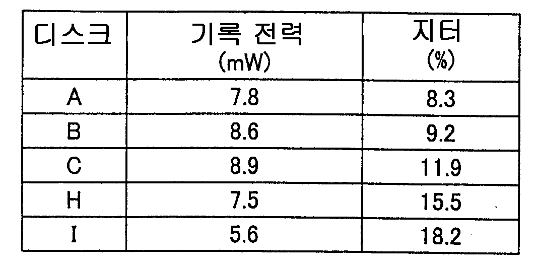
비교예 H 및 I 에 비하여 충분한 지터값을 나타내는 실시형태 A 내지 C 을 획득하였다.Embodiments A to C showing sufficient jitter values were obtained as compared with Comparative Examples H and I.
도 10 은 TEM 사진에서의 BiGeN 기록층 상의 기록 마크를 나타내며, 도 11 은 TEM 사진에서의 SnTiN 기록층 (광디스크 A) 상의 기록 마크를 나타낸다. 두 사진으로부터, 기록 마크가 기록 시 안내홈으로 확장되지 않고 서브 미크론의 기공으로 형성되는 것을 알 수 있다. 또한, AFM (미도시) 으로 관찰한 결과 비기록부와 기록부 사이의 높이 차이가 27 nm 의 안내홈에 대하여 대략 6 nm 였다.Fig. 10 shows recording marks on a BiGeN recording layer in a TEM picture, and Fig. 11 shows recording marks on a SnTiN recording layer (optical disk A) in a TEM picture. From the two photographs, it can be seen that the recording mark is formed by the pores of the sub micron, rather than extending into the guide groove during recording. In addition, as a result of observing with AFM (not shown), the height difference between the non-recorded portion and the recorded portion was approximately 6 nm with respect to the guide groove of 27 nm.
샘플 광디스크의 BiGeN 기록층 상의 질화물 및 산화물과 함께 Ge 및 Bi 를 ESCA 에 투입하였으며, 그 측정 결과를 표 6 에 나타냈다. 표 6 에 기초하여, 도 12 는 비질화물 및 첨가된 질화물양에 대한 Ge 질화물의 함량 퍼센트의 변화를 나타내며, 도 13 은 비질화물 (Bi 및 그 산화물) 및 첨가된 질화물양에 대한 Bi 질화물의 함량 퍼센트의 변화를 나타낸다.Ge and Bi were added to ESCA together with nitrides and oxides on the BiGeN recording layer of the sample optical disk, and the measurement results are shown in Table 6. Based on Table 6, FIG. 12 shows the change in the content percentage of Ge nitride with respect to the amount of non-nitride and added nitride, and FIG. 13 shows the content of Bi nitride for the amount of non-nitride (Bi and its oxide) and added nitride Represents a percentage change.

전술한 결과는 증착 시 질소 도입량이 5 sccm 인 경우 금속 Ge 가 잔류하는 것을 나타낸다. 금속 Ge 가 화학 분석시에 기록층 상에서 산화되어 Ge-O 조성으로 생성되는 비질화물이 존재한다. 금속 Ge 는 증착 시 질소 도입량이 10 sccm 일 때 실질적으로 존재하지 않으며, 단지 질소 도입량이 20 sccm 이상일 때 Ge-N 성분이 관찰된다.The above results indicate that the metal Ge remains when the amount of nitrogen introduced during deposition is 5 sccm. There is a non-nitride in which the metal Ge is oxidized on the recording layer in chemical analysis to produce a Ge-O composition. Metal Ge is substantially absent when the amount of nitrogen introduced during deposition is 10 sccm, only Ge-N component is observed when the amount of nitrogen introduced is 20 sccm or more.
구체적으로, 질소 도입량이 10 sccm 이상일 때 기록막 중에 85 % 이상의 Ge 가 질화된다. 보다 다량의 질소를 도입할 때, 증착 속도가 떨어지므로, 질소 도입량이 10 내지 80 sccm 인 경우에 효과적이도록 한다. 기록층이 충분한 흡수를 제공할 수 있는 범위는 기록 감도 측면을 고려할 때, 질소 도입량이 10 내지 60 sccm 인 것이 바람직하다.Specifically, more than 85% of Ge is nitrided in the recording film when the nitrogen introduction amount is 10 sccm or more. When introducing a larger amount of nitrogen, the deposition rate is lowered, so that it is effective when the amount of nitrogen introduced is 10 to 80 sccm. The range in which the recording layer can provide sufficient absorption is preferably from 10 to 60 sccm, in consideration of the recording sensitivity.
유사하게, 도 6 은 증착 시 질소 도입량이 5 sccm 일 때 금속 Bi 가 잔존하는 것을 나타낸다. 기록막에서, Bi 는 금속 Bi 및 Bi-N 조성의 혼합물에 존재하고, 질화물의 퍼센트는 증착 시 질소 도입량의 증가에 따라 증가된다.Similarly, FIG. 6 shows that the metal Bi remains when the amount of nitrogen introduced during deposition is 5 sccm. In the recording film, Bi is present in the mixture of the metal Bi and Bi-N compositions, and the percentage of nitride increases with increasing nitrogen introduction amount upon deposition.
증착 시 질소 도입량이 80 sccm 일 때, 약 94 % 의 Bi 가 질화된다. 따라서, 85 % 이상의 Ge 가 질화되고 94 % 이하의 Bi 가 질화되는 것이 바람직하다. 또한, 증착 시 질소 도입량이 60 sccm 인 경우 85 % 의 Ge 가 질화되고 90 % 이하의 Bi 가 질화되는 것이, 기록 감도를 향상시키기에 바람직하다.When the amount of nitrogen introduced during deposition is 80 sccm, about 94% of Bi is nitrided. Therefore, it is preferable that 85% or more of Ge are nitrided and 94% or less of Bi is nitrided. In addition, when the amount of nitrogen introduced during deposition is 60 sccm, it is preferable that 85% of Ge is nitrided and 90% or less of Bi is nitrided to improve recording sensitivity.
따라서, 기록층 내의 금속 성분비는 넓은 범위이므로 (20 내지 40 at% 의 금속 질화물 범위와 같은 고온 분해 조성물의 범위), 우수한 특성을 갖는다. 그러나, 고온 분해 화합물이 질화물을 구성할 때, 증착 시 막이 완전하게 질화되도록 질소 유량을 조절하는 것이 필요하다.Therefore, since the metal component ratio in the recording layer is in a wide range (in the range of the high temperature decomposition composition such as the metal nitride range of 20 to 40 at%), it has excellent characteristics. However, when the high temperature decomposition compound constitutes nitride, it is necessary to adjust the nitrogen flow rate so that the film is completely nitrided upon deposition.
첨가되는 질소의 유량비가 증가할 때, 비질화 성분은 저온 분해 질화물에서 감소되어, 기록층의 흡수율을 감소시킨다. 그 결과, 고온 분해 화합물이 질화물로 구성될 때, 기록층의 감도가 열화되고 막 증착 속도가 감소되어, 층 생산성이 저하된다. 따라서, 질소 첨가량은 가능한한 생산성이 유리하도록 조절되어야 하다.When the flow rate ratio of nitrogen added is increased, the non-nitriding component is reduced in low temperature decomposition nitride, thereby reducing the absorption rate of the recording layer. As a result, when the high temperature decomposition compound is made of nitride, the sensitivity of the recording layer is deteriorated and the film deposition rate is reduced, resulting in a decrease in layer productivity. Therefore, the nitrogen addition amount should be adjusted so that productivity is as advantageous as possible.
도 14 는 기록층의 고온 분해 화합물을 금속 질화물로 구성하는 경우의 반응 스퍼터링 조건을 설정하는 방법을 나타낸다. 먼저, 이러한 금속 질화물에 포함되는 금속 성분을 포함하는 합금 또는 그 산화물 또는 그 질화물으로 구성되는 스퍼터링 타겟을 제공한다. 예를 들면, 합금 타겟을 스퍼터링 장치의 챔버에 제공한다 (SS1). 다음으로, 스퍼터링 주입 가스에 따른 소정의 초기값에 기초하여 Ar 가스 및 질소 가스 유량비를 결정한다 (SS2). 다음으로, 반응 스퍼터링 증착을 형성한다 (SS3). 다음으로, 증착된 기록층의 조성을 분석한다 (SS4). 다음으로, 고온 분해 화합물이 완전하게 질화되었는지의 여부를 결정한다 (SS5). 여기서, 고온 분해 화합물이 완전히 질화되지 않았다면 유량 결정 단계 (SS2) 로 되돌아감으로써, 질소 가스의 유량비를 증가시켜, 완전하게 질화되도록 한다. 그 반면, 고온 분해 화합물이 완전하게 질화되지 않았다면 비질화된 저온 분해 질화물의 성분이 층이 존재하는지의 여부를 결정한다 (SS6). 여기서, 비질화된 저온 분해 질화물의 성분이 불충분하다면, 유량 결정 단계 (SS2) 로 되돌아가서, 질소 가스 유량을 감소시켜, 비질화된 성분이 기록층에 존재하도록 한다. 그 반면, 비질화된 성분이 기록층에 충분히 있다면 질소 가스의 유량을 결정하여 (SS7), 기록층의 증착 조건 설정이 완료된다. 기록층의 제조 단계에서 결정된 질소 가스의 유량으로 기록층의 제조 단계로 진행한다. 또한, 금속 질화물과 다른 재료를 기록층에 이용하는 경우에 전술한 증착 조건의 설정 방법을 이용할 수 있다.Fig. 14 shows a method of setting reaction sputtering conditions when the high temperature decomposition compound of the recording layer is composed of metal nitride. First, an sputtering target composed of an alloy containing a metal component contained in such a metal nitride, an oxide thereof, or a nitride thereof is provided. For example, an alloy target is provided to the chamber of the sputtering apparatus (SS1). Next, Ar gas and nitrogen gas flow volume ratio are determined based on the predetermined | prescribed initial value according to sputtering injection gas (SS2). Next, a reactive sputter deposition is formed (SS3). Next, the composition of the deposited recording layer is analyzed (SS4). Next, it is determined whether the hot decomposition compound is completely nitrided (SS5). Here, if the high temperature decomposition compound has not been completely nitrided, the flow rate determination step SS2 is increased to increase the flow rate ratio of the nitrogen gas so as to be completely nitrided. On the other hand, if the pyrolytic compound is not fully nitrided, the component of the non-nitrided cryolytic nitride determines whether a layer is present (SS6). Here, if the components of the non-nitridated low-temperature decomposition nitride are insufficient, the flow returns to the flow rate determination step SS2 to reduce the nitrogen gas flow rate so that the non-nitridated components are present in the recording layer. On the other hand, if there are enough non-nitridated components in the recording layer, the flow rate of nitrogen gas is determined (SS7), and setting of the deposition conditions of the recording layer is completed. The flow of the nitrogen gas determined in the manufacturing step of the recording layer proceeds to the manufacturing step of the recording layer. In addition, when the metal nitride and other materials are used for the recording layer, the above-described method for setting the deposition conditions can be used.
도 15 는 기록층을 증착하기 위하여 PP (packing plate) 상에 고정되는 디스크형 형체 (T) 를 갖는 스퍼터링용 타겟의 단면도를 나타낸다. 타겟을 균질 합금 또는 질화물 또는 산화물로 형성할 수 있다. 다른 방법으로, 스퍼터링 수율의 관점에서 볼 때 타겟을 복수의 단체 조각으로 모자이크 형성할 수 있다.Fig. 15 shows a sectional view of a target for sputtering having a disk-shaped shape T fixed on a packing plate (PP) for depositing a recording layer. The target may be formed of a homogeneous alloy or nitride or oxide. Alternatively, the target may be mosaicd into a plurality of single pieces in terms of sputtering yield.
본 발명에 따르면, 조사광의 기록 레이저 전력으로 인하여 분해가 용이한 금속 질화물 (저온 분해 질화물) 및 분해가 어려운 금속 화합물 (고온 분해 화합물) 로 구성되는 기록층과 같은 혼합층에 의해 열 분해를 제어할 수 있다. 따라서, 미소 변형을 나타내는 도 10 및 도 11 에 나타낸 바와 같이 이러한 층 구성은 기록 후 우수한 형상을 갖는 미세 마크를 제공한다. 주로, 열 분해 후 기록층의 광학 특성 변화로서 정보 기록이 달성된다. 따라서, 기록 전후에 현저한 반사율의 차이 및 높은 S/N 비율 및 우수한 지터 특성을 갖는 기록층을 획득한다.According to the present invention, thermal decomposition can be controlled by a mixed layer such as a recording layer composed of a metal nitride (low temperature decomposition nitride) that is easily decomposed due to the recording laser power of the irradiation light and a metal compound (high temperature decomposition compound) that is difficult to decompose. have. Thus, as shown in Figs. 10 and 11 showing the micro deformation, this layer configuration provides fine marks having excellent shape after recording. Mainly, information recording is achieved as a change in optical properties of the recording layer after thermal decomposition. Thus, a recording layer having a significant difference in reflectance and a high S / N ratio and excellent jitter characteristics before and after recording is obtained.
또한, 타겟 함유량을 조절하여 질소 첨가되는 반응 스퍼터링 증착 시 혼합된 기록층을 한번에 형성할 수 있다.In addition, by adjusting the target content, the mixed recording layer can be formed at a time during reaction sputtering deposition to which nitrogen is added.
또한, 환경 기준에서 유해물로서 설정되지 않은 무기 재료로부터 기록층의 성분을 선택할 수 있다. In addition, the components of the recording layer can be selected from inorganic materials not set as harmful substances in environmental standards.
전술한 설명 및 첨부된 도면이 본 발명의 바람직한 실시형태로 설정되는 것이다. 당업자는 개시된 발명의 정신 및 범위로부터 벗어나지 않는다면 전술한 기술을 조명하여 다양한 변형, 추가 및 다른 설계를 행할 수 있는 것은 자명하다. 따라서, 본 발명은 개시된 실시형태로 제한되지 않으며 첨부된 특허청구범위의 범위 전체 내에서 실시될 수 있다는 것은 자명하다.The foregoing description and the annexed drawings set forth in preferred embodiments of the invention. It will be apparent to those skilled in the art that various modifications, additions, and other designs may be made to the above teachings without departing from the spirit and scope of the disclosed invention. Therefore, it is to be understood that the invention is not limited to the disclosed embodiments but may be practiced within the scope of the appended claims.
Claims (23)
Applications Claiming Priority (5)
| Application Number | Priority Date | Filing Date | Title |
|---|---|---|---|
| JP2002162047 | 2002-06-03 | ||
| JPJP-P-2002-00162047 | 2002-06-03 | ||
| JPJP-P-2003-00024139 | 2003-01-31 | ||
| JP2003024139 | 2003-01-31 | ||
| PCT/JP2003/006439 WO2003101750A1 (en) | 2002-06-03 | 2003-05-23 | Information recording medium and process for producing the same |
Publications (2)
| Publication Number | Publication Date |
|---|---|
| KR20050009734A KR20050009734A (en) | 2005-01-25 |
| KR100709931B1 true KR100709931B1 (en) | 2007-04-24 |
Family
ID=29714331
Family Applications (1)
| Application Number | Title | Priority Date | Filing Date |
|---|---|---|---|
| KR1020047019759A KR100709931B1 (en) | 2002-06-03 | 2003-05-23 | Information recording medium and process for producing the same |
Country Status (10)
| Country | Link |
|---|---|
| US (1) | US7524612B2 (en) |
| EP (1) | EP1510355B1 (en) |
| JP (1) | JP3810076B2 (en) |
| KR (1) | KR100709931B1 (en) |
| CN (2) | CN101320576B (en) |
| AU (1) | AU2003242414A1 (en) |
| DE (1) | DE60311804T2 (en) |
| HK (1) | HK1072037A1 (en) |
| TW (1) | TWI236674B (en) |
| WO (1) | WO2003101750A1 (en) |
Families Citing this family (22)
| Publication number | Priority date | Publication date | Assignee | Title |
|---|---|---|---|---|
| JP2005044450A (en) * | 2003-07-24 | 2005-02-17 | Tdk Corp | Optical recording medium and method for manufacturing same, and data recording method and data reproducing method for optical recording medium |
| WO2005018947A1 (en) * | 2003-08-21 | 2005-03-03 | Mitsubishi Kagaku Media Co., Ltd. | Recording medium |
| US7952984B2 (en) | 2004-04-22 | 2011-05-31 | Tdk Corporation | Optical recording medium and method of recording and reproducing of optical recording medium |
| US7427431B2 (en) * | 2004-04-28 | 2008-09-23 | Sony Corporation | Write once optical recording medium |
| JP2006281751A (en) * | 2004-04-28 | 2006-10-19 | Sony Corp | Write-once optical recording medium |
| US7235501B2 (en) | 2004-12-13 | 2007-06-26 | Micron Technology, Inc. | Lanthanum hafnium oxide dielectrics |
| JP2006018986A (en) * | 2005-01-20 | 2006-01-19 | Pioneer Electronic Corp | Optical recording medium and its manufacturing method |
| US7803445B2 (en) | 2005-02-23 | 2010-09-28 | Pioneer Corporation | Optical recording medium |
| US7972974B2 (en) | 2006-01-10 | 2011-07-05 | Micron Technology, Inc. | Gallium lanthanide oxide films |
| JP4560495B2 (en) * | 2006-06-16 | 2010-10-13 | 三菱化学メディア株式会社 | recoding media |
| US7759747B2 (en) | 2006-08-31 | 2010-07-20 | Micron Technology, Inc. | Tantalum aluminum oxynitride high-κ dielectric |
| US7605030B2 (en) | 2006-08-31 | 2009-10-20 | Micron Technology, Inc. | Hafnium tantalum oxynitride high-k dielectric and metal gates |
| US7563730B2 (en) | 2006-08-31 | 2009-07-21 | Micron Technology, Inc. | Hafnium lanthanide oxynitride films |
| US7776765B2 (en) | 2006-08-31 | 2010-08-17 | Micron Technology, Inc. | Tantalum silicon oxynitride high-k dielectrics and metal gates |
| US7544604B2 (en) | 2006-08-31 | 2009-06-09 | Micron Technology, Inc. | Tantalum lanthanide oxynitride films |
| US8124211B2 (en) | 2007-03-28 | 2012-02-28 | Ricoh Company, Ltd. | Optical recording medium, sputtering target, and method for manufacturing the same |
| JP4577581B2 (en) * | 2007-08-30 | 2010-11-10 | ソニー株式会社 | Optical information recording medium |
| JP2009143184A (en) * | 2007-12-17 | 2009-07-02 | Kobe Steel Ltd | Recording layer for optical information recording medium and optical information recording medium |
| WO2009104239A1 (en) * | 2008-02-18 | 2009-08-27 | 株式会社 東芝 | Non-volatile storage device and its manufacturing method |
| JP4969624B2 (en) | 2008-11-12 | 2012-07-04 | 株式会社神戸製鋼所 | Optical information recording medium |
| WO2011034153A1 (en) | 2009-09-18 | 2011-03-24 | 株式会社神戸製鋼所 | Recording layer for optical information recording medium, optical information recording medium, and sputtering target |
| JP5399836B2 (en) | 2009-09-18 | 2014-01-29 | 株式会社神戸製鋼所 | Recording layer for optical information recording medium, optical information recording medium, and sputtering target |
Citations (2)
| Publication number | Priority date | Publication date | Assignee | Title |
|---|---|---|---|---|
| JPS6211685A (en) * | 1985-07-10 | 1987-01-20 | Mitsubishi Chem Ind Ltd | Optical recording medium |
| JPH02165991A (en) * | 1988-12-20 | 1990-06-26 | Akira Tazaki | Optical recording medium and manufacture thereof |
Family Cites Families (28)
| Publication number | Priority date | Publication date | Assignee | Title |
|---|---|---|---|---|
| US4188214A (en) * | 1975-08-11 | 1980-02-12 | Fuji Photo Film Co., Ltd. | Recording material |
| US4470053A (en) * | 1981-02-13 | 1984-09-04 | Minnesota Mining And Manufacturing Company | Protuberant optical recording medium |
| JPS6134741A (en) * | 1984-07-09 | 1986-02-19 | アメリカン テレフォン アンド テレグラフ カムパニー | Medium for storage of information |
| JPS62114133A (en) * | 1985-11-13 | 1987-05-25 | Hitachi Maxell Ltd | Additional writing type disk for information recording |
| US4839208A (en) * | 1986-04-30 | 1989-06-13 | Nec Corporation | Optical information recording medium |
| JPS6363153A (en) * | 1986-09-03 | 1988-03-19 | Nec Corp | Production of optical recording medium |
| JPS63299984A (en) * | 1987-05-30 | 1988-12-07 | Kuraray Co Ltd | Optical recording medium and production thereof |
| US5034255A (en) * | 1988-10-28 | 1991-07-23 | Mitsui Petrochemical Industries, Ltd. | Optical recording medium and method of its production |
| JPH02147392A (en) * | 1988-11-30 | 1990-06-06 | Toshiba Corp | Information recording medium |
| JPH02215587A (en) * | 1989-02-17 | 1990-08-28 | Toshiba Corp | Optical information recording medium |
| JPH02277689A (en) | 1989-04-20 | 1990-11-14 | Toshiba Corp | Optical data recording medium |
| JPH03153389A (en) * | 1989-11-09 | 1991-07-01 | Kuraray Co Ltd | Optical recording medium |
| JP2836227B2 (en) * | 1990-09-11 | 1998-12-14 | 松下電器産業株式会社 | Optical recording medium and method for producing the same, and sputtering target for optical recording medium and method for producing the same |
| US5232566A (en) * | 1991-05-14 | 1993-08-03 | International Business Machines Corporation | Underlayer doping in thin film magnetic recording media |
| JP3088168B2 (en) * | 1991-12-13 | 2000-09-18 | ティーディーケイ株式会社 | Optical recording medium and manufacturing method thereof |
| JPH05212967A (en) * | 1992-02-04 | 1993-08-24 | Dainippon Printing Co Ltd | Optical reocrding medium and production thereof |
| US5334433A (en) * | 1992-12-28 | 1994-08-02 | Tdk Corporation | Optical recording medium |
| JP3026327B2 (en) * | 1996-07-25 | 2000-03-27 | インダストリアル テクノロジー リサーチ インスティチュート | Write-once optical disc and optical recording medium |
| JPH10222871A (en) * | 1997-02-06 | 1998-08-21 | Denso Corp | Optical information recording medium and its production |
| JPH10329424A (en) * | 1997-06-04 | 1998-12-15 | Denso Corp | Optical information recording medium and its manufacture |
| JP3570169B2 (en) * | 1997-08-22 | 2004-09-29 | 松下電器産業株式会社 | Optical information recording medium |
| JPH11138996A (en) * | 1997-11-12 | 1999-05-25 | Toyota Central Res & Dev Lab Inc | Storage member |
| JP3697896B2 (en) * | 1998-01-23 | 2005-09-21 | 株式会社デンソー | Optical information recording medium and manufacturing method thereof |
| JPH11232692A (en) * | 1998-02-10 | 1999-08-27 | Sony Corp | Optical record medium and manufacture thereof |
| US5972458A (en) * | 1998-04-01 | 1999-10-26 | Eastman Kodak Company | Optical recording element with an interfacial layer between the recording layer and the reflecting layer |
| US6335071B1 (en) * | 1998-07-14 | 2002-01-01 | Kabushiki Kaisha Toyota Chuo Kenkyusho | Storage member |
| TW484126B (en) * | 1999-03-26 | 2002-04-21 | Matsushita Electric Ind Co Ltd | Manufacturing and recording regeneration method for information record medium |
| WO2005018947A1 (en) * | 2003-08-21 | 2005-03-03 | Mitsubishi Kagaku Media Co., Ltd. | Recording medium |
-
2003
- 2003-05-23 KR KR1020047019759A patent/KR100709931B1/en active IP Right Grant
- 2003-05-23 US US10/516,244 patent/US7524612B2/en active Active
- 2003-05-23 CN CN2008101273000A patent/CN101320576B/en not_active Expired - Lifetime
- 2003-05-23 WO PCT/JP2003/006439 patent/WO2003101750A1/en active IP Right Grant
- 2003-05-23 JP JP2004509072A patent/JP3810076B2/en not_active Expired - Lifetime
- 2003-05-23 EP EP03733031A patent/EP1510355B1/en not_active Expired - Lifetime
- 2003-05-23 DE DE60311804T patent/DE60311804T2/en not_active Expired - Lifetime
- 2003-05-23 AU AU2003242414A patent/AU2003242414A1/en not_active Abandoned
- 2003-05-23 CN CN038127903A patent/CN1659041A/en active Pending
- 2003-05-30 TW TW092114819A patent/TWI236674B/en not_active IP Right Cessation
-
2005
- 2005-06-13 HK HK05104914A patent/HK1072037A1/en not_active IP Right Cessation
Patent Citations (2)
| Publication number | Priority date | Publication date | Assignee | Title |
|---|---|---|---|---|
| JPS6211685A (en) * | 1985-07-10 | 1987-01-20 | Mitsubishi Chem Ind Ltd | Optical recording medium |
| JPH02165991A (en) * | 1988-12-20 | 1990-06-26 | Akira Tazaki | Optical recording medium and manufacture thereof |
Also Published As
| Publication number | Publication date |
|---|---|
| HK1072037A1 (en) | 2005-08-12 |
| AU2003242414A1 (en) | 2003-12-19 |
| EP1510355B1 (en) | 2007-02-14 |
| DE60311804D1 (en) | 2007-03-29 |
| DE60311804T2 (en) | 2007-10-31 |
| JPWO2003101750A1 (en) | 2005-09-29 |
| CN101320576B (en) | 2012-07-11 |
| WO2003101750A1 (en) | 2003-12-11 |
| EP1510355A4 (en) | 2005-07-13 |
| US7524612B2 (en) | 2009-04-28 |
| CN101320576A (en) | 2008-12-10 |
| US20050233247A1 (en) | 2005-10-20 |
| TW200402711A (en) | 2004-02-16 |
| JP3810076B2 (en) | 2006-08-16 |
| EP1510355A1 (en) | 2005-03-02 |
| TWI236674B (en) | 2005-07-21 |
| KR20050009734A (en) | 2005-01-25 |
| CN1659041A (en) | 2005-08-24 |
Similar Documents
| Publication | Publication Date | Title |
|---|---|---|
| KR100709931B1 (en) | Information recording medium and process for producing the same | |
| EP0978831B1 (en) | Optical information recording medium and method for producing the same, method for recording and reproducing information thereon and recording/reproducing apparatus | |
| EP1215669B1 (en) | Optical information recording medium, method for producing the same, and method and apparatus for recording information thereon | |
| EP0195532A1 (en) | An information recording medium | |
| EP1414029A2 (en) | Optical recording medium and method for manufacturing the same | |
| EP1394786B1 (en) | Optical recording medium and method for optically recording data in the same | |
| US20020076646A1 (en) | Optical information medium and its use | |
| EP1345218B1 (en) | Optical information recording medium and manufacturing method and recording/reproducing method for the same | |
| KR100614505B1 (en) | Rewritable optical information medium | |
| EP1426940B1 (en) | Optical information recording medium and recording method using it | |
| US7615333B2 (en) | Write-once optical disk and optical recording method | |
| JPWO2004032130A1 (en) | Optical information recording medium and manufacturing method thereof | |
| EP1350245A1 (en) | Optical information medium and its use | |
| JP3889028B2 (en) | Information recording medium | |
| JP2006182030A (en) | Information recording medium | |
| US20070076579A1 (en) | Optical storage medium | |
| JP3608934B2 (en) | Optical recording medium and protective film for optical recording medium | |
| JP2002352472A (en) | Optical information recording medium, its manufacturing method and its recording/reproducing method | |
| US20060165946A1 (en) | Optical storage medium | |
| EP1059634A1 (en) | Optical recording medium and protective film therefor | |
| JPH10208296A (en) | Optical recording medium | |
| JPH11314455A (en) | Light recording medium | |
| JPH10235997A (en) | Phase-changing optical recording medium | |
| KR19980043937A (en) | Method of manufacturing phase change type optical recording medium | |
| JPH08267925A (en) | Optical recording medium and production thereof |
Legal Events
| Date | Code | Title | Description |
|---|---|---|---|
| A201 | Request for examination | ||
| E902 | Notification of reason for refusal | ||
| E701 | Decision to grant or registration of patent right | ||
| GRNT | Written decision to grant | ||
| FPAY | Annual fee payment |
Payment date: 20130321 Year of fee payment: 7 |
|
| FPAY | Annual fee payment |
Payment date: 20140319 Year of fee payment: 8 |
|
| FPAY | Annual fee payment |
Payment date: 20160318 Year of fee payment: 10 |
|
| FPAY | Annual fee payment |
Payment date: 20170317 Year of fee payment: 11 |