JP3762352B2 - Wiring board - Google Patents
Wiring board Download PDFInfo
- Publication number
- JP3762352B2 JP3762352B2 JP2002302175A JP2002302175A JP3762352B2 JP 3762352 B2 JP3762352 B2 JP 3762352B2 JP 2002302175 A JP2002302175 A JP 2002302175A JP 2002302175 A JP2002302175 A JP 2002302175A JP 3762352 B2 JP3762352 B2 JP 3762352B2
- Authority
- JP
- Japan
- Prior art keywords
- insulating base
- copper
- wiring conductor
- molybdenum
- tungsten
- Prior art date
- Legal status (The legal status is an assumption and is not a legal conclusion. Google has not performed a legal analysis and makes no representation as to the accuracy of the status listed.)
- Expired - Fee Related
Links
Images


Classifications
-
- H—ELECTRICITY
- H01—ELECTRIC ELEMENTS
- H01L—SEMICONDUCTOR DEVICES NOT COVERED BY CLASS H10
- H01L2224/00—Indexing scheme for arrangements for connecting or disconnecting semiconductor or solid-state bodies and methods related thereto as covered by H01L24/00
- H01L2224/01—Means for bonding being attached to, or being formed on, the surface to be connected, e.g. chip-to-package, die-attach, "first-level" interconnects; Manufacturing methods related thereto
- H01L2224/26—Layer connectors, e.g. plate connectors, solder or adhesive layers; Manufacturing methods related thereto
- H01L2224/31—Structure, shape, material or disposition of the layer connectors after the connecting process
- H01L2224/32—Structure, shape, material or disposition of the layer connectors after the connecting process of an individual layer connector
- H01L2224/321—Disposition
- H01L2224/32151—Disposition the layer connector connecting between a semiconductor or solid-state body and an item not being a semiconductor or solid-state body, e.g. chip-to-substrate, chip-to-passive
- H01L2224/32221—Disposition the layer connector connecting between a semiconductor or solid-state body and an item not being a semiconductor or solid-state body, e.g. chip-to-substrate, chip-to-passive the body and the item being stacked
- H01L2224/32225—Disposition the layer connector connecting between a semiconductor or solid-state body and an item not being a semiconductor or solid-state body, e.g. chip-to-substrate, chip-to-passive the body and the item being stacked the item being non-metallic, e.g. insulating substrate with or without metallisation
-
- H—ELECTRICITY
- H01—ELECTRIC ELEMENTS
- H01L—SEMICONDUCTOR DEVICES NOT COVERED BY CLASS H10
- H01L2224/00—Indexing scheme for arrangements for connecting or disconnecting semiconductor or solid-state bodies and methods related thereto as covered by H01L24/00
- H01L2224/01—Means for bonding being attached to, or being formed on, the surface to be connected, e.g. chip-to-package, die-attach, "first-level" interconnects; Manufacturing methods related thereto
- H01L2224/42—Wire connectors; Manufacturing methods related thereto
- H01L2224/47—Structure, shape, material or disposition of the wire connectors after the connecting process
- H01L2224/48—Structure, shape, material or disposition of the wire connectors after the connecting process of an individual wire connector
- H01L2224/4805—Shape
- H01L2224/4809—Loop shape
- H01L2224/48091—Arched
-
- H—ELECTRICITY
- H01—ELECTRIC ELEMENTS
- H01L—SEMICONDUCTOR DEVICES NOT COVERED BY CLASS H10
- H01L2224/00—Indexing scheme for arrangements for connecting or disconnecting semiconductor or solid-state bodies and methods related thereto as covered by H01L24/00
- H01L2224/01—Means for bonding being attached to, or being formed on, the surface to be connected, e.g. chip-to-package, die-attach, "first-level" interconnects; Manufacturing methods related thereto
- H01L2224/42—Wire connectors; Manufacturing methods related thereto
- H01L2224/47—Structure, shape, material or disposition of the wire connectors after the connecting process
- H01L2224/48—Structure, shape, material or disposition of the wire connectors after the connecting process of an individual wire connector
- H01L2224/481—Disposition
- H01L2224/48151—Connecting between a semiconductor or solid-state body and an item not being a semiconductor or solid-state body, e.g. chip-to-substrate, chip-to-passive
- H01L2224/48221—Connecting between a semiconductor or solid-state body and an item not being a semiconductor or solid-state body, e.g. chip-to-substrate, chip-to-passive the body and the item being stacked
- H01L2224/48225—Connecting between a semiconductor or solid-state body and an item not being a semiconductor or solid-state body, e.g. chip-to-substrate, chip-to-passive the body and the item being stacked the item being non-metallic, e.g. insulating substrate with or without metallisation
- H01L2224/48227—Connecting between a semiconductor or solid-state body and an item not being a semiconductor or solid-state body, e.g. chip-to-substrate, chip-to-passive the body and the item being stacked the item being non-metallic, e.g. insulating substrate with or without metallisation connecting the wire to a bond pad of the item
-
- H—ELECTRICITY
- H01—ELECTRIC ELEMENTS
- H01L—SEMICONDUCTOR DEVICES NOT COVERED BY CLASS H10
- H01L2224/00—Indexing scheme for arrangements for connecting or disconnecting semiconductor or solid-state bodies and methods related thereto as covered by H01L24/00
- H01L2224/73—Means for bonding being of different types provided for in two or more of groups H01L2224/10, H01L2224/18, H01L2224/26, H01L2224/34, H01L2224/42, H01L2224/50, H01L2224/63, H01L2224/71
- H01L2224/732—Location after the connecting process
- H01L2224/73251—Location after the connecting process on different surfaces
- H01L2224/73265—Layer and wire connectors
Description
【0001】
【発明の属する技術分野】
本発明は半導体素子やコンデンサ、抵抗器等の電子部品が搭載される配線基板に関するものである。
【0002】
【従来の技術】
従来、電子部品、例えば、半導体素子が搭載される配線基板は、酸化アルミニウム質焼結体から成り、その表面に半導体素子が搭載される搭載部を有する絶縁基体と、該絶縁基体の半導体素子搭載部またはその周辺から下面にかけて導出されている、例えば、タングステンやモリブデン等の高融点金属粉末から成る複数個の配線導体と、絶縁基体の下面に形成され、前記配線導体と電気的に接続されている複数個の接続パッドとから構成されており、絶縁基体の搭載部に半導体素子をガラス、樹脂、ロウ材等から成る接着材を介して接着固定させるとともに半導体素子の各電極をボンディングワイヤ等の電気的接続手段を介して配線導体に電気的に接続し、しかる後、必要に応じて前記半導体素子を蓋体や封止樹脂で気密封止させることによって半導体装置となる。
【0003】
かかる半導体装置は、外部電気回路基板上に、該外部電気回路基板の回路配線と絶縁基体下面の接続パッドとが、間に錫−鉛半田等の低融点ロウ材を挟んで対向するよう載置させ、しかる後、前記低融点ロウ材を約200℃〜300℃の温度で加熱溶融させ、外部電気回路基板の回路配線と絶縁基体下面の接続パッドとを接合させることによって外部電気回路基板上に実装され、同時に配線基板に搭載されている半導体素子の各電極も配線導体および低融点ロウ材を介して外部電気回路基板に電気的に接続されることとなる。
【0004】
しかしながら、上記従来の半導体素子が搭載される配線基板は絶縁基体が酸化アルミニウム質焼結体で形成されるとともに、配線導体および接続パッドがタングステンやモリブデン等の高融点金属で形成されており、該高融点金属は電気抵抗が高い(電気抵抗率(20℃)で、タングステン:5.5×10⁻⁶Ω・cm、モリブデン:5.7×10⁻⁶Ω・cm)ことから接続パッドや配線導体を、半導体素子の演算速度の高速化等に対応して十分に低抵抗とすることができないという欠点があった。
【0005】
そこで、この従来の欠点を解決する方法として、本出願人は先に酸化アルミニウムを主成分とする相対密度が95%以上のセラミックスから成る絶縁基体と、該絶縁基体の表面および/または内部に銅を10〜70体積%、タングステンおよび/またはモリブデンを30〜90体積%の割合で含有したメタライズ層(接続パッド、配線導体)を具備する配線基板およびその製造方法を提案した(特開2000−188453号参照)。
【0006】
この配線基板によれば、メタライズ層(接続パッド、配線導体)が低抵抗の銅を含有するため接続パッドや配線導体を形成する導体の電気抵抗を低く(電気抵抗率(20℃)で約3×10⁻⁶〜5×10⁻⁶Ω・cm)することができ、また絶縁基体が酸化アルミニウム質焼結体等から成り、かつ相対密度が高く緻密であるため熱伝導性を高くすることもできる。
【0007】
このような配線基板は、例えば、酸化アルミニウムを主成分とし、酸化マンガン(MnO2)を2.0〜6.0重量%の割合で含有するセラミック成分をシート状に成形して得た複数枚のセラミックグリーンシートの表面に、銅粉末を10〜70体積%、平均粒径が1〜10μmのタングステンおよび/またはモリブデンを30〜90体積%の割合で含有してなる導電ペーストを印刷塗布し、このセラミックグリーンシートを上下に積層するとともに、非酸化成雰囲気中で1200〜1500℃の温度で焼成することによって製作される。
【0008】
【特許文献1】
特開平11−111886号公報
【特許文献2】
特開2000−188453号公報
【0009】
【発明が解決しようとする課題】
しかしながら、上記配線基板は、接続パッドや配線導体を低抵抗とすることができるものの接続パッドや配線導体の主成分である銅の融点以上の温度で焼成されることから銅粉末同士が融着し、銅粉末の絶縁基体に対する焼結一体化が不十分なものとなり、接続パッドや配線導体の絶縁基体に対する接着強度が低いものであった。
【0010】
また、上記配線基板は絶縁基体が酸化アルミニウム質焼結体等のセラミックス材料で形成されており、その熱膨張係数が約4×10⁻⁶/℃〜10×10-6/℃であるのに対し、外部電気回路基板は一般にガラスエポキシ樹脂等の樹脂材で形成されており、その熱膨張係数が30×10-6/℃〜50×10-6/℃であり、大きく相違することから、外部電気回路基板上に半導体装置を実装した後、半導体素子の作動時に発する熱が配線基板の絶縁基体と外部電気回路基板に繰り返し作用すると、両者間に両者の熱膨張係数の差に起因して水平方向に大きな熱応力が繰り返し生じるとともにこの熱応力が接続パッドの外周縁に沿って集中する。
【0011】
そしてその結果、接続パッドが、外周縁部分から捲れるようにして、絶縁基体の表面から剥がれ、半導体素子と外部電気回路との電気的接続が短期間で破れてしまうという問題があった。
【0012】
特に、低融点ロウ材として、従来の錫−鉛半田に代わり、錫−銀−ビスマス系等の鉛非含有半田が用いられるようになると、このような鉛非含有半田は硬く変形しにくいため熱応力を吸収緩和する作用が弱く、接続パッドに作用する熱応力が従来の錫−鉛半田の場合に比べて大きくなるため、接続パッドの剥がれの発生がより顕著なものとなってしまう。
【0013】
【課題を解決するための手段】
本発明の配線基板は、電気絶縁材料から成り、表面に電子部品が搭載される搭載部を有する絶縁基体と、該絶縁基体の下面に形成されている多数の接続パッドと、前記絶縁基体の前記搭載部から前記接続パッドにかけて導出されている複数個の配線導体とから成る配線基板であって、前記各接続パッドは、タングステンおよび/またはモリブデンと銅とから成る前記配線導体と直接接続する主接続部と、タングステンおよび/またはモリブデンと鉄族金属とから成る前記主接続部の外周部と前記絶縁基体の表面との間に介在する補助接続部とにより形成されていることを特徴とするものである。
【0014】
本発明の配線基板によれば、各接続パッドを、タングステンおよび/またモリブデンと銅とから成る前記配線導体と直接接続する主接続部と、タングステンおよび/またはモリブデンと鉄族金属とから成る前記主接続部の外周部と前記絶縁基体の表面との間に介在する補助接続部とにより形成し、前記主接続部が低抵抗の銅を主成分として含有していることから、接続パッドを低抵抗とすることができる。
【0015】
また同時に、前記接続パッドは、前記主接続部の外周部と絶縁基体の表面との間に、絶縁基体および主接続部に対し強固に接合することが可能なタングステンおよび/またはモリブデンと鉄族金属とから成る補助接続部を介在させたことから、この補助接続部を介して主接続部の外周部を絶縁基体に対して強固に接合させておくことができ、接続パッドに対して熱応力が作用したとしても、その外周部から剥がれが発生することを効果的に防止することができ、配線基板の外部電気回路基板に対する接続信頼性を高くすることができる。
【0016】
【発明の実施の形態】
次に本発明を添付の図面を基にして詳細に説明する。
【0017】
図1は、本発明の配線基板を使用した半導体素子収納用パッケージの一実施例を示す断面図であり、1は絶縁基体、2は配線導体である。この絶縁基体1と配線導体2とで半導体素子3を搭載する配線基板4が構成される。
【0018】
前記絶縁基体1は、例えば酸化アルミニウム質焼結体、窒化アルミニウム質焼結体、炭化珪素質焼結体等のセラミック焼結体により形成され、その上面に半導体素子3が搭載収容される搭載部1aを有し、該搭載部1a底面には半導体素子3がガラスや樹脂、ロウ材等の接着材を介して接着固定される。
【0019】
前記絶縁基体1は、その熱伝導性および機械的強度を良好とする上では、相対密度95%以上の高緻密体から構成されるものであることが望ましい。
【0020】
更に本発明では、前記絶縁基体1は、配線導体2との同時焼成による保形性を達成する上では、1200℃乃至1500℃の低温で焼成することが必要となるが、本発明によれば、このような低温での焼成においても相対密度95%以上に緻密化することが望ましい。
【0021】
かかる観点から、本発明における絶縁基体1は、例えば、酸化アルミニウムを主成分とするもの、具体的には酸化アルミニウムを90重量%以上の割合で含有するものが好適に使用され、第2の成分として、Mn化合物をMnO2換算で2.0乃至6.0質量%の割合で含有するものが望ましい。即ち、マンガン化合物が2.0質量%よりも少ないと、1200℃乃至1500℃での緻密化が達成されにくく、また6.0質量%よりも多いと絶縁基体1の絶縁性が低下する。マンガン化合物の最適な範囲はMnO2換算で3乃至7重量%である。
【0022】
また、この絶縁基体1中には、第3の成分として、SiO2およびMgO、CaO、SrO等のアルカリ土類元素酸化物を低温焼結性を高めるために合計で0.4乃至8質量%の割合で含有せしめることが望ましい。
【0023】
さらに、この絶縁基体1中には、着色成分や誘電率などの誘電特性の向上のためにW、Mo、Crなどの金属を着色成分とし2質量%以下の割合で含んでもよい。
【0024】
上記酸化アルミニウム以外の成分は、酸化アルミニウム主結晶相の粒界に非晶質相あるいは結晶相として存在するが、熱伝導性を高める上で粒界中に助剤成分を含有する結晶相が形成されていることが望ましい。
【0025】
また前記絶縁基体1を酸化アルミニウムを主成分として形成した場合、酸化アルミニウム主結晶相は、粒状または柱状の結晶として存在するが、これら主結晶相の平均結晶粒径は、1.5乃至5.0μmであることが望ましい。
【0026】
なお、主結晶相が柱状結晶からなる場合、上記平均結晶粒径は、短軸径に基づくものである。この主結晶相の平均結晶粒径が1.5μmよりも小さいと、高熱伝導化が難しく、平均粒径が5.0μmよりも大きいと基板材料として用いる場合に要求される十分な強度が得られにくくなるためである。
【0027】
このような絶縁基体1は、例えば、酸化アルミニウムを主成分とする原料粉末に有機バインダーや溶媒を添加してスラリー(泥漿状物)となすとともに、これをドクターブレード法等でシート状に成形して得たセラミックグリーンシートを非酸化性雰囲気中、1200℃〜1500℃の温度で焼成することにより形成される。
【0028】
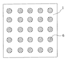
また前記絶縁基体1は、図2に示すように、その搭載部1a周辺から下面にかけて多数の配線導体2が被着形成されており、該配線導体2の搭載部1a周辺部位には半導体素子3の各電極がボンディングワイヤ5を介して電気的に接続され、また絶縁基体1下面に導出された部位には配線導体2と電気的に接続する複数の接続パッド6が形成されている。
【0029】
前記配線導体2は、半導体素子3の電極を外部に導出する作用をなし、また前記接続パッド6は、配線基板4を外部電気回路基板に実装する外部端子として作用し、低融点ロウ材を介して外部電気回路基板の回路配線に接合され、これにより半導体素子3の電極が外部電気回路基板の回路配線と電気的に接続される。
【0030】
前記配線導体2は、タングステン、モリブデン、銅等の金属材料から成り、配線導体2を低抵抗とするとともに、酸化アルミニウム質焼結体から成る絶縁基体1との同時焼成による形成を可能とする上では、タングステンおよび/またはモリブデンと銅とにより形成することが好ましい。
【0031】
前記配線導体2は、絶縁基体1となるセラミックグリーンシートにタングステンおよび/またはモリブデン粉末と、銅粉末とを所定の割合で有機溶剤、バインダーとともに混練してなる導電ペーストを前記セラミックグリーンシートの表面にスクリーン印刷法等により印刷塗布することにより形成することができる。
【0032】
前記配線導体2は、銅を10乃至70体積%、タングステン及び/またはモリブデンを30乃至90体積%の割合で含有することが望ましい。これは、配線導体2の低抵抗化と、上記絶縁基体1との同時焼結性を達成するとともに、特に配線導体2の同時焼成時の保形成を維持するためであり、上記銅量が10体積%よりも少なく、タングステンやモリブデン量が90体積%よりも多いと、配線導体2の抵抗が高く(電気抵抗率で約5.5×10-6Ω・cm以上)なる。また銅量が70体積%よりも多く、タングステンやモリブデン量が30体積%よりも少ないと、配線導体2の、特に絶縁基体1表面に露出した部分で、同時焼成時の保形成が低下し、配線導体2においてにじみが発生したり、溶融した銅によって配線導体2が凝集して断線が生じるとともに、絶縁基体1と配線導体2との熱膨張系数差により配線導体2の剥離が発生するためである。最適な組成範囲は、銅を40乃至60体積%、タングステンおよび/またはモリブデンを60乃至40体積%である。
【0033】
また、本発明においては、配線導体2中におけるタングステンおよび/またはモリブデンは、平均粒径1乃至10μmの球状あるいは数個の粒子による焼結粒子として銅からなるマトリックス中に分散含有していることが望ましい。これは、上記平均粒径が、1μmよりも小さい場合、配線導体2の保形性が悪くなるとともに組織が多孔質化し、配線導体2の抵抗が高くなり、10μmを越えると銅のマトリックスがタングステンやモリブデンの粒子によって分断されてしまい配線導体2の抵抗が高くなったり、銅成分が分離してにじみなどが発生するためである。タングステンおよび/またはモリブデンは平均粒径1.3乃至5μm、特に1.3乃至3μmの大きさで分散されていることが最も望ましい。
【0034】
また、上記配線導体2中には、絶縁基体1との密着性を改善するために、アルミナ、または絶縁基体1と同じ成分のセラミックスを0.05乃至2体積%の割合で含有させることも可能である。
【0035】
さらに、本発明の配線基板4においては、銅を含有する配線導体2を銅の融点を越える温度で絶縁基体1と同時焼成することにより、配線導体2中の銅成分が絶縁基体1中に拡散する場合があるが、本発明によれば、上記少なくとも銅を含む配線導体2の周囲のセラミックスへの銅の拡散距離が20μm以下、特に10μm以下であることが望ましい。これは、銅のセラミックス中への拡散距離が20μmを越えると、電気回路形成時に配線導体2間の絶縁性が低下し電気回路の信頼性が低下するためである。
【0036】
この銅の拡散距離を20μm以下とすることにより、配線導体2のうち、同一平面内に形成された各配線導体2間の最小線間距離を100μm以下、特に90μm以下の高密度化を図ることができる。
【0037】
また、本発明の配線基板4においては、図3、図4に示すように、各接続パッド6を、タングステンおよび/またはモリブデンと銅とから成る前記配線導体2と直接接続する主接続部6aと、タングステンおよび/またはモリブデンと鉄族金属とから成る前記主接続部6aの外周部と前記絶縁基体1の表面との間に介在する補助接続部6bとにより形成することが重要である。
【0038】
各接続パッド6を、タングステンおよび/またはモリブデンと銅とから成る配線導体2と直接接続する主接続部6aと、タングステンおよび/またはモリブデンと鉄族金属とから成る前記主接続部6aの外周部と絶縁基体1の表面との間に介在する補助接続部6bとにより形成しておくと、前記主接続部6aが低抵抗の銅を主成分として含有していることから、接続パッド6を低抵抗とすることができ、低融点ロウ材と接続パッド6との接触抵抗を低くすることができる。また、前記補助接続部6bは、絶縁基体1および主接続部6aのいずれに対しても強固に接合することが可能なタングステンおよび/またはモリブデンと鉄族金属とから成り、主接続部6aの外周部と絶縁基体1表面との間に介在して両者と接合することから、主接続部6aの外周部を絶縁基体1に対して強固に接合させる接合材として作用し、接続パッド6に対して熱応力が作用したとしても、その外周部から剥がれが発生することを効果的に防止することができ、配線基板4の外部電気回路基板に対する接続信頼性を高くすることができる。
【0039】
前記接続パッド6の主接続部6aは、配線導体2と直接接続しており、配線導体2を外部に接続させるための主導体として作用し、前記絶縁基体1の下面となるセラミックグリーンシート表面にタングステンおよび/またはモリブデン粉末と、銅粉末とを所定の割合で有機溶剤、バインダーとともに混練してなる導電ペーストを前記セラミックグリーンシートの表面にスクリーン印刷法等により印刷塗布することにより形成することができる。
【0040】
この場合、接続パッド6の主接続部6aは、上記配線導体2をタングステンおよび/またはモリブデンと銅とにより形成する場合と同様の材料を用いることが望ましく、例えば、銅を10乃至70体積%、タングステン及び/またはモリブデンを30乃至90体積%の割合で含有することが望ましい。また、タングステンおよび/またはモリブデンは、平均粒径1乃至10μmの球状あるいは数個の粒子による焼結粒子として銅からなるマトリックス中に分散含有していることが望ましい。さらに、アルミナ、または絶縁基体1と同じ成分のセラミックスを0.05乃至2体積%の割合で含有させることも可能である。
【0041】
また、前記接続パッド6は、前記主接続部6aの外周縁と絶縁基体1の表面との間に、絶縁基体1および主接続部6aに対し強固に接合することが可能なタングステンおよび/またはモリブデンと鉄族金属とから成る補助接続部6bが介在していることから、主接続部6aの外周部を絶縁基体1に対して強固に接合させておくことができ、接続パッド6に対して熱応力が作用したとしても、その外周部から剥がれが発生することを効果的に防止することができ、配線基板4の外部電気回路基板に対する接続信頼性を高くすることができる。
【0042】
この場合、配線導体2および低融点ロウ材と直接接続するのが、銅を含有し低抵抗の主接続部6aであるため、接続パッド6と絶縁基体1との間の接合を強固とするとともに、配線導体2と低融点ロウ材との間の導通抵抗や接触抵抗を低く維持することができる。
【0043】
なお、前記接続パッド6の補助接続部6bは、主接続部6aおよび配線導体2と同時焼成によって形成する場合、その焼成温度が1200〜1500℃の低温で焼成する必要がある。そのため本発明ではこれを達成するため補助接続部6bを、タングステンおよび/またはモリブデンに、鉄族金属を含有せしめている。
【0044】
前記補助接続部6bを、タングステンおよび/またはモリブデンに、鉄族金属を含有せしめて形成すると低温での焼成性を高めて絶縁基体1と同時焼成によって、また絶縁基体1に対し密着強度を強固として形成することができる。
【0045】
前記補助接続部6bは鉄族金属の量が酸化物換算で0.1体積%未満の場合には補助接続部6bの緻密化が進行せず焼結不良になって絶縁基体1との接着強度が低下する。逆に、5体積%を超える場合には、タングステン、モリブデンの粒子が異常粒成長し絶縁基体1との接着強度が低下する。従って、上記鉄族金属の量は、酸化物換算で0.1乃至5体積%、好適には0.5乃至2体積%としておくことが望ましい。
【0046】
なお上記補助接続部6b中の鉄族金属としては、鉄、ニッケル、コバルトが挙げられるがこれらの中でもニッケルが最も望ましい。また酸化物換算量は、鉄(Fe)はFe2O3、ニッケル(Ni)はNiO、コバルト(Co)はCo3O4の形態で換算した量である。
【0047】
更に、この補助接続部6b中には、酸化アルミニウム等を主成分とする絶縁基体1との接着強度を高めるために、酸化アルミニウム等の絶縁基体1と同種のセラミック粉末を添加することも有効である。しかし、その含有量が45体積%よりも多いと焼結不良を招くおそれがある。従って、補助接続部6bに酸化アルミニウムを添加する場合、その含有量は特に2乃至35体積%が望ましい。
【0048】
なお、前記補助接続部6bは、主接続部6aの外縁から100μm以上の幅で絶縁基体1表面との間に介在するようにして形成しておくことが好ましい。主接続部6aと絶縁基体1表面との間に介在する補助接続部6bの、主接続部6a外縁からの幅が100μm未満となると、接合幅が狭いため、主接続部6aの絶縁基体1に対する被着を効果的に強固なものとすることが困難となる。
【0049】
また、前記補助接続部6bは、前記主接続部6aの外縁から外側に延出させるようにして形成してもよい。このように補助接続部6bを延出させておくと、接続パッド6(主接続部6a)が、例えば直径1mm以下の円形等に、非常に小さくなってきたとしても、補助接続部6bと絶縁基体1表面との接合幅を十分に確保することができ、接続パッド6と絶縁基体1との接合の信頼性をより一層確実に確保することができる。また、このように補助接続部6bを主接続部6aの外縁より外側に延出させる場合、隣接する接続パッド6の補助接続部6bとの間の隣接間隔を50μm以上確保するようにしておくことが好ましい。この隣接間隔が50μm未満となると隣接する接続パッド6間の電気絶縁性が低下するおそれがある。
【0050】
また、前記接続パッド6は、円形または楕円形としておくと、外周の一部に熱応力が集中して、その部分から剥がれを生じることを効果的に防止することができ、配線基板4としての信頼性をより一層確実に優れたものとすることができる。したがって、前記接続パッド6は、円形または楕円形としておくことが好ましい。
【0051】
この場合、前記接続パッド6の主接続部6aと補助接続部6bとは、同心円状として、主接続部6aの外周部の全周をほぼ同じ幅で補助接続部6bを介して絶縁基体1表面に接合させるようにしてもよく、また、長軸方向が絶縁基体1下面の対角線方向(熱応力が大きく作用する方向)となるような楕円状とし、熱応力が大きく作用する方向で、接続パッド6と絶縁基体1、および接続パッド6と低融点ロウ材の接合の強度をより高めるようにしてもよい。
【0052】
また、前記配線導体2および接続パッド6の主接続部6a、補助接続部6bは、その露出表面をニッケル、銅、金等のめっき金属層で被覆するようにしておくと、配線導体2および接続パッド6の酸化腐食を防止することができるとともに、配線導体2に対するボンディングワイヤ5のボンディング性や接続パッド6に対する低融点ロウ材の濡れ性等を良好とすることができる。従って、前記配線導体2および接続パッド6の主接続部6a、補助接続部6bは、その露出表面をニッケル、銅、金等のめっき金属層(図示せず)で被覆しておくことが好ましい。
【0053】
この場合、各めっき金属層は全領域で均一な層構成、厚みとする必要はなく、各被着される部位に応じて、適宜、層構成や厚み等を変えるようにしてもよい。
【0054】
例えば、配線導体2を、高周波信号の伝送等に対応するため、より一層低抵抗とする場合であれば、配線導体2の表面に銅めっき層を2μm乃至15μm、特に3μm乃至6μm程度の厚みで被着させるようにしておくことが好ましく、接続パッド6に対する低融点ロウ材の濡れ性を良好とする場合には、ニッケルめっき層3〜8μm、金めっき層を0.3〜0.8μmの厚みで、順次被着させるようにしておくことが好ましい。
(製造方法)
次に、上記配線基板4の製造方法の一例を、絶縁基体1が酸化アルミニウム質焼結体から成る場合について具体的に説明する。
【0055】
まず、絶縁基体1を形成するために、セラミックス焼結体の主成分となる酸化アルミニウム原料粉末として、平均粒径が0.5μm乃至2.5μm、特に0.5μm乃至2.0μmの粉末を用いる。これは、平均粒径は0.5μmよりも小さいと、粉末の取扱いが難しく、また粉末のコストが高くなり、2.5μmよりも大きいと、1500℃以下の温度で焼成することが難しくなるためである。
【0056】
そして、上記酸化アルミニウム粉末に対して、第2の成分として、MnO2を2.0乃至8.0重量%、特に3.0乃至7.0重量%の割合で添加する。また適宜、第3の成分として、SiO2.MgO、CaO、SrO2粉末等を0.4乃至8重量%、第4の成分として、W、Mo、Crなどの遷移金属の金属粉末や酸化物粉末を着色成分として金属換算で2重量%以下の割合で添加する。
【0057】
なお、上記酸化物の添加にあたっては、酸化物粉末以外に、焼成によって酸化物を形成し得る炭酸塩、硝酸塩、酢酸塩などとして添加してもよい。
【0058】
そして次に、この混合粉末を用いて絶縁基体1を形成するためのセラミックグリーンシートを複数枚作製する。セラミックグリーンシートは、周知の成形方法によって作製することができる。例えば、上記混合粉末に有機バインダーや溶媒を添加してスラリーを調整した後、ドクターブレード法によって形成したり、混合粉末に有機バインダーを加え、プレス成形、圧延成形等により所定の厚みのセラミックグリーンシートを作製できる。
【0059】
このようにして作製したセラミックグリーンシートに対して、まず、配線導体2となる導体成分として、平均粒径が1乃至10μmの銅粉末を10乃至70体積%、特に40乃至60体積%、平均粒径が1乃至10μmのタングステンおよび/またはモリブデン粉末を30乃至90体積%、特に40乃至60体積%の割合で添加してなる固形成分に対して有機バインダーや溶剤を添加混合することにより作製した導電ペーストを調整し、このペーストを前記セラミックグリーンシートの表面にスクリーン印刷、グラビア印刷等の手法によって印刷塗布する。
【0060】
なお、前記導電ペースト中には、絶縁基体1との密着性を高めるために、酸化アルミニウム粉末や、絶縁基体1を形成する酸化物セラミックス成分と同一の組成物粉末を0.05〜2体積%の割合で添加することも可能である。
【0061】
次に、接続パッド6の補助接続部6bとなる導電ペーストを、セラミックグリーンシート表面のうち、主接続部6aとなる導電ペーストの印刷予定領域の外周部に、環状等の所定のパターンに印刷塗布する。
【0062】
なお、前記補助接続部6bとなる導電ペーストは、例えば、平均粒径が0.5〜5μmのタングステンおよび/またはモリブデンに、酸化ニッケル等の鉄族金属の酸化物粉末を0.1〜5体積%、アルミナ粉末を0〜45体積%の割合で含有する固形成分に対して、有機バインダーや溶剤を添加混合することにより作製される。
【0063】
その後、前記配線導体2となる導電ペーストと同様の導電ペーストを、セラミックグリーンシートの表面および印刷した補助接続部6bとなる導電ペーストの表面に、接続パッド6の主接続部6aの所定パターンに印刷する。この場合、主接続部6aのパターンに印刷された導電ペーストは、その外周部で、下側に補助接続部6bとなる導電ペーストが印刷されているため、外周が盛り上がった形状となるが、この印刷した導電ペーストに対して加圧加工を施すことにより、平坦に均すことができ、接続パッド6としての上面の平坦度を確保することができる。
【0064】
そして最後に、各配線導体2、主接続部6a、補助接続部6bとなる導電ペーストを印刷塗布したセラミックグリーンシートを位置合わせして積層圧着した後、この積層体を、非酸化性雰囲気中、焼成最高温度が1200〜1500℃の温度となる条件で焼成する。
【0065】
このときの上記焼成温度が1200℃より低いと、通常の原料を用いた場合において、酸化アルミニウム質焼結体から成る絶縁基体が相対密度95%以上まで緻密化できず、熱伝導性や機械的強度が低下し、1500℃よりも高いと、配線導体2および接続パッド6の主接続部6aにおいて、タングステンあるいはモリブデン自体の焼結が進み、銅との均一組織を維持できなく、ひいては低抵抗を維持することが困難となりシート抵抗や低融点ロウ材との接触抵抗等が高くなってしまう。また、酸化物セラミックスの主結晶相の粒径が大きくなり異常粒成長が発生したり、銅がセラミックス中へ拡散するときのパスである粒界の長さが短くなるとともに拡散速度も速くなる結果、拡散距離を30μm以下に制御することが困難となるためである。好適には1350〜1450℃の範囲がよい。
【0066】
また、この焼成時の非酸化性雰囲気としては、窒素、あるいは窒素と水素との混合雰囲気であることが望ましいが、特に、配線導体2や主接続部6a中の銅の拡散を抑制する上では、水素および窒素を含み露点+10℃以下、特に−10℃以下の非酸化性雰囲気であることが望ましい。なお、この雰囲気には所望により、アルゴンガス等の不活性ガスを混入してもよい。焼成時の露点が+10℃より高いと、焼成中に酸化物セラミックスと雰囲気中の水分とが反応し酸化膜を形成し、この酸化膜と銅含有導体の銅が反応してしまい、導体の低抵抗化の妨げとなるのみでなく、銅の拡散を助長してしまうためである。
【0067】
さらにまた、上記のように焼成温度および雰囲気を制御して焼成することによって、絶縁基体1の表面の算術平均粗さRaを1μm以下、特に0.7μm以下の平滑性に優れた表面を形成できる。
【0068】
かくして本発明の配線基板によれば、絶縁基体1の搭載部1a底面に半導体素子3をガラスや樹脂、ロウ材等の接着剤を介して接着固定するとともにこの半導体素子3の各電極を配線導体2にボンディングワイヤ5を介して電気的に接続し、しかる後、絶縁基体1の上面に金属やセラミックスから成る蓋体7をガラスや樹脂、ロウ材等の封止材を介して接合させ、絶縁基体1と蓋体7とから成る容器内部に半導体素子3を気密に収容することによって製品としての半導体装置が完成する。
【0069】
なお、本発明の配線基板は上述の実施の形態に限定されるものではなく、本発明の要旨を逸脱しない範囲であれば種々の変更は可能であり、例えば、上記の実施例では本発明の配線基板を半導体素子収納用パッケージに用いた例について説明したが、これを混成集積回路基板等に用いてもよい。
【0070】
【発明の効果】
本発明の配線基板によれば、各接続パッドを、タングステンおよび/またはモリブデンと銅とから成る前記配線導体と直接接続する主接続部と、タングステンおよび/またはモリブデンと鉄族金属とから成る前記主接続部の外周部と前記絶縁基体の表面との間に介在する補助接続部とにより形成し、前記主接続部が低抵抗の銅を主成分として含有していることから、接続パッドを低抵抗とすることができる。
【0071】
また同時に、前記接続パッドは、前記主接続部の外周部と絶縁基体の表面との間に、絶縁基体および主接続部に対し強固に接合することが可能なタングステンおよび/またはモリブデンと鉄族金属とから成る補助接続部を介在させたことから、この補助接続部を介して主接続部の外周部を絶縁基体に対して強固に接合させておくことができ、接続パッドに対して熱応力が作用したとしても、その外周部から剥がれが発生することを効果的に防止することができ、配線基板の外部電気回路基板に対する接続信頼性を高くすることができる。
【図面の簡単な説明】
【図1】本発明の配線基板の一実施例を示す断面図である。
【図2】図1に示す配線基板の下面図である。
【図3】図1に示す配線基板の要部拡大断面図である。
【図4】図1に示す配線基板の要部拡大下面図である。
【符号の説明】
1・・・・絶縁基体
1a・・・搭載部
2・・・・配線導体
3・・・・半導体素子
4・・・・配線基板
5・・・・ボンディングワイヤ
6・・・・接続パッド
6a・・・主接続部
6b・・・補助接続部
7・・・・蓋体[0001]
BACKGROUND OF THE INVENTION
The present invention relates to a wiring board on which electronic components such as a semiconductor element, a capacitor, and a resistor are mounted.
[0002]
[Prior art]
2. Description of the Related Art Conventionally, an electronic component, for example, a wiring board on which a semiconductor element is mounted is made of an aluminum oxide sintered body, and has an insulating substrate having a mounting portion on which the semiconductor element is mounted, and the semiconductor element mounting of the insulating substrate. A plurality of wiring conductors made of a refractory metal powder such as tungsten or molybdenum, which are led out from the portion or its periphery to the lower surface, and formed on the lower surface of the insulating base and electrically connected to the wiring conductor. The semiconductor element is bonded and fixed to the mounting portion of the insulating base via an adhesive made of glass, resin, brazing material, etc., and each electrode of the semiconductor element is bonded to a bonding wire or the like. By electrically connecting to the wiring conductor via an electrical connection means, and then sealing the semiconductor element with a lid or a sealing resin as necessary. A semiconductor device Te.
[0003]
Such a semiconductor device is placed on an external electric circuit board such that the circuit wiring of the external electric circuit board and the connection pads on the lower surface of the insulating base are opposed to each other with a low melting point solder such as tin-lead solder interposed therebetween. After that, the low melting point brazing material is heated and melted at a temperature of about 200 ° C. to 300 ° C., and the circuit wiring of the external electric circuit board and the connection pads on the lower surface of the insulating base are bonded to each other on the external electric circuit board. Each electrode of the semiconductor element that is mounted and simultaneously mounted on the wiring board is also electrically connected to the external electric circuit board via the wiring conductor and the low melting point brazing material.
[0004]
However, in the wiring board on which the conventional semiconductor element is mounted, the insulating base is formed of an aluminum oxide sintered body, and the wiring conductor and the connection pad are formed of a refractory metal such as tungsten or molybdenum. Refractory metals have high electrical resistance (electrical resistivity (20 ° C.), tungsten: 5.5 × 10 -6 Ω · cm, molybdenum: 5.7 × 10 -6 (Ω · cm), the connection pads and wiring conductors have a drawback that they cannot be made sufficiently low resistance in response to an increase in the operation speed of the semiconductor elements.
[0005]
Therefore, as a method for solving this conventional defect, the present applicant has previously described an insulating base composed of ceramics mainly composed of aluminum oxide and having a relative density of 95% or more, and copper on the surface and / or inside of the insulating base. Proposed is a wiring board having a metallized layer (connection pad, wiring conductor) containing 10 to 70% by volume of tungsten and / or 30 and 90% by volume of tungsten and / or molybdenum (Japanese Patent Laid-Open No. 2000-188453). Issue).
[0006]
According to this wiring board, since the metallized layer (connection pad, wiring conductor) contains low-resistance copper, the electrical resistance of the conductor forming the connection pad or wiring conductor is low (electric resistivity (20 ° C.) of about 3). × 10 -6 ~ 5x10 -6 Ω · cm), and the insulating base is made of an aluminum oxide sintered body and the like, and the relative density is high and the heat conductivity can be increased.
[0007]
Such a wiring board has, for example, aluminum oxide as a main component and manganese oxide (MnO 2 ) On the surface of a plurality of ceramic green sheets obtained by molding a ceramic component containing 2.0 to 6.0% by weight of a copper component, 10 to 70% by volume of copper powder and an average particle size of A conductive paste containing 1 to 10 μm of tungsten and / or molybdenum in a proportion of 30 to 90% by volume is printed and applied, and the ceramic green sheets are laminated on top and bottom, and 1200 to 1500 ° C. in a non-oxidizing atmosphere. It is manufactured by firing at a temperature of
[0008]
[Patent Document 1]
JP-A-11-111886
[Patent Document 2]
JP 2000-188453 A
[0009]
[Problems to be solved by the invention]
However, although the above wiring board can reduce the resistance of the connection pad and the wiring conductor, the copper powder is fused to each other because it is fired at a temperature equal to or higher than the melting point of copper which is the main component of the connection pad and the wiring conductor. Further, the integration of sintering of the copper powder with respect to the insulating base was insufficient, and the bonding strength of the connection pad and the wiring conductor to the insulating base was low.
[0010]
Further, the wiring board has an insulating base made of a ceramic material such as an aluminum oxide sintered body, and its thermal expansion coefficient is about 4 × 10. -6 / ° C.-10 × 10 -6 The external electric circuit board is generally formed of a resin material such as glass epoxy resin, and its thermal expansion coefficient is 30 × 10. -6 / ° C to 50 × 10 -6 After mounting a semiconductor device on an external electric circuit board, the heat generated during operation of the semiconductor element repeatedly acts on the insulating substrate of the wiring board and the external electric circuit board. A large thermal stress is repeatedly generated in the horizontal direction due to the difference between the thermal expansion coefficients of the two, and this thermal stress is concentrated along the outer peripheral edge of the connection pad.
[0011]
As a result, there is a problem that the connection pad is peeled off from the surface of the insulating base so as to bend from the outer peripheral edge portion, and the electrical connection between the semiconductor element and the external electric circuit is broken in a short period of time.
[0012]
In particular, when lead-free solder such as tin-silver-bismuth is used instead of conventional tin-lead solder as the low melting point brazing material, such lead-free solder is hard and not easily deformed. Since the effect of absorbing and relaxing the stress is weak and the thermal stress acting on the connection pad is larger than in the case of conventional tin-lead solder, the occurrence of peeling of the connection pad becomes more prominent.
[0013]
[Means for Solving the Problems]
The wiring board of the present invention is made of an electrically insulating material, and has an insulating base having a mounting portion on which an electronic component is mounted, a large number of connection pads formed on the lower surface of the insulating base, and the insulating base. A wiring board comprising a plurality of wiring conductors led out from the mounting portion to the connection pad, wherein each connection pad is directly connected to the wiring conductor comprising tungsten and / or molybdenum and copper. And an auxiliary connecting portion interposed between the outer peripheral portion of the main connecting portion made of tungsten and / or molybdenum and an iron group metal and the surface of the insulating base. is there.
[0014]
According to the wiring board of the present invention, each connection pad is directly connected to the wiring conductor made of tungsten and / or molybdenum and copper, and the main pad made of tungsten and / or molybdenum and an iron group metal. It is formed by an auxiliary connection part interposed between the outer peripheral part of the connection part and the surface of the insulating base, and the main connection part contains low resistance copper as a main component. It can be.
[0015]
At the same time, the connection pad includes tungsten and / or molybdenum and an iron group metal that can be firmly bonded to the insulating base and the main connecting portion between the outer peripheral portion of the main connecting portion and the surface of the insulating base. Therefore, the outer peripheral portion of the main connection portion can be firmly bonded to the insulating base via the auxiliary connection portion, and thermal stress is applied to the connection pad. Even if it acts, it can prevent effectively that peeling from the outer peripheral part occurs, and the connection reliability of the wiring board to the external electric circuit board can be increased.
[0016]
DETAILED DESCRIPTION OF THE INVENTION
The present invention will now be described in detail with reference to the accompanying drawings.
[0017]
FIG. 1 is a cross-sectional view showing an embodiment of a package for housing a semiconductor element using a wiring board of the present invention, wherein 1 is an insulating substrate and 2 is a wiring conductor. The insulating
[0018]
The insulating
[0019]
The insulating
[0020]
Furthermore, in the present invention, the insulating
[0021]
From this point of view, the insulating
[0022]
Further, in this insulating
[0023]
Further, the insulating
[0024]
Components other than the above-mentioned aluminum oxide exist as an amorphous phase or a crystalline phase at the grain boundary of the aluminum oxide main crystal phase, but a crystal phase containing an auxiliary component is formed in the grain boundary in order to improve thermal conductivity. It is desirable that
[0025]
When the insulating
[0026]
In addition, when the main crystal phase is composed of columnar crystals, the average crystal grain size is based on the minor axis diameter. When the average crystal grain size of the main crystal phase is smaller than 1.5 μm, it is difficult to achieve high thermal conductivity, and when the average grain size is larger than 5.0 μm, sufficient strength required for use as a substrate material can be obtained. This is because it becomes difficult.
[0027]
For example, such an insulating
[0028]
As shown in FIG. 2, the insulating
[0029]
The
[0030]
The
[0031]
The
[0032]
The
[0033]
Further, in the present invention, tungsten and / or molybdenum in the
[0034]
Further, in order to improve the adhesion to the insulating
[0035]
Furthermore, in the
[0036]
By setting the copper diffusion distance to 20 μm or less, the minimum distance between the wiring
[0037]
Further, in the
[0038]
A
[0039]
The
[0040]
In this case, the
[0041]
Further, the
[0042]
In this case, since the
[0043]
In addition, when the
[0044]
When the auxiliary connecting
[0045]
When the amount of the iron group metal is less than 0.1% by volume in terms of oxide, the
[0046]
Examples of the iron group metal in the
[0047]
Further, it is also effective to add the same kind of ceramic powder as that of the insulating
[0048]
The auxiliary connecting
[0049]
The auxiliary connecting
[0050]
Further, if the
[0051]
In this case, the
[0052]
Further, the
[0053]
In this case, it is not necessary for each plated metal layer to have a uniform layer configuration and thickness in the entire region, and the layer configuration, thickness, and the like may be changed as appropriate according to each portion to be deposited.
[0054]
For example, if the
(Production method)
Next, an example of a method for manufacturing the
[0055]
First, in order to form the insulating
[0056]
And as a 2nd component with respect to the said aluminum oxide powder, MnO 2 Is added at a ratio of 2.0 to 8.0% by weight, particularly 3.0 to 7.0% by weight. As appropriate, as the third component, SiO 2 . MgO, CaO, SrO 2 0.4 to 8% by weight of powder or the like is added as a fourth component, and a metal powder or oxide powder of a transition metal such as W, Mo, or Cr is added as a coloring component in a proportion of 2% by weight or less in terms of metal.
[0057]
In addition to the oxide powder, the oxide may be added as carbonate, nitrate, acetate, or the like that can form an oxide by firing.
[0058]
Next, a plurality of ceramic green sheets for forming the insulating
[0059]
With respect to the ceramic green sheet thus produced, first, as a conductor component to be the
[0060]
In the conductive paste, 0.05 to 2% by volume of aluminum oxide powder or the same composition powder as the oxide ceramic component forming the insulating
[0061]
Next, the conductive paste to be the
[0062]
The conductive paste to be the
[0063]
Thereafter, the same conductive paste as the conductive paste to be the
[0064]
And finally, after aligning and laminating and pressing the ceramic green sheet printed and coated with the conductive paste to be each
[0065]
If the firing temperature at this time is lower than 1200 ° C., when an ordinary raw material is used, the insulating base made of the aluminum oxide sintered body cannot be densified to a relative density of 95% or more, and thermal conductivity or mechanical If the strength decreases and the temperature is higher than 1500 ° C., the sintering of tungsten or molybdenum itself proceeds in the
[0066]
Further, the non-oxidizing atmosphere at the time of firing is preferably nitrogen or a mixed atmosphere of nitrogen and hydrogen. In particular, in suppressing the diffusion of copper in the
[0067]
Furthermore, by controlling the baking temperature and atmosphere as described above, baking can be performed with an arithmetic average roughness Ra of the surface of the insulating
[0068]
Thus, according to the wiring board of the present invention, the
[0069]
The wiring board of the present invention is not limited to the above-described embodiment, and various modifications can be made without departing from the gist of the present invention. Although the example in which the wiring board is used for the package for housing semiconductor elements has been described, this may be used for a hybrid integrated circuit board or the like.
[0070]
【The invention's effect】
According to the wiring board of the present invention, each connection pad is connected directly to the wiring conductor made of tungsten and / or molybdenum and copper, and the main pad made of tungsten and / or molybdenum and an iron group metal. It is formed by an auxiliary connection part interposed between the outer peripheral part of the connection part and the surface of the insulating base, and the main connection part contains low resistance copper as a main component. It can be.
[0071]
At the same time, the connection pad includes tungsten and / or molybdenum and an iron group metal that can be firmly bonded to the insulating base and the main connecting portion between the outer peripheral portion of the main connecting portion and the surface of the insulating base. Therefore, the outer peripheral portion of the main connection portion can be firmly bonded to the insulating base via the auxiliary connection portion, and thermal stress is applied to the connection pad. Even if it acts, it can prevent effectively that peeling from the outer peripheral part occurs, and the connection reliability of the wiring board to the external electric circuit board can be increased.
[Brief description of the drawings]
FIG. 1 is a cross-sectional view showing an embodiment of a wiring board according to the present invention.
2 is a bottom view of the wiring board shown in FIG. 1. FIG.
3 is an enlarged cross-sectional view of a main part of the wiring board shown in FIG.
4 is an enlarged bottom view of the main part of the wiring board shown in FIG. 1. FIG.
[Explanation of symbols]
1. Insulating substrate
1a: Mounting part
2 ... Wiring conductor
3 .... Semiconductor element
4 ... Wiring board
5 ... Bonding wire
6 ... Connection pads
6a ... Main connection part
6b ... Auxiliary connection
7 ··· Lid
Claims (1)
前記各接続パッドは、タングステンおよび/またはモリブデンと銅とから成る前記配線導体と直接接続する主接続部と、タングステンおよび/またはモリブデンと鉄族金属とから成る前記主接続部の外周部と前記絶縁基体の表面との間に介在する補助接続部とにより形成されていることを特徴とする配線基板。An insulating base made of an electrically insulating material and having a mounting portion on which an electronic component is mounted, a number of connection pads formed on the lower surface of the insulating base, and from the mounting portion of the insulating base to the connection pad A wiring board composed of a plurality of derived wiring conductors,
Each of the connection pads includes a main connection portion directly connected to the wiring conductor made of tungsten and / or molybdenum and copper, an outer peripheral portion of the main connection portion made of tungsten and / or molybdenum and an iron group metal, and the insulation. A wiring board, characterized in that it is formed by an auxiliary connection portion interposed between the surface of the substrate.
Priority Applications (1)
| Application Number | Priority Date | Filing Date | Title |
|---|---|---|---|
| JP2002302175A JP3762352B2 (en) | 2002-10-16 | 2002-10-16 | Wiring board |
Applications Claiming Priority (1)
| Application Number | Priority Date | Filing Date | Title |
|---|---|---|---|
| JP2002302175A JP3762352B2 (en) | 2002-10-16 | 2002-10-16 | Wiring board |
Publications (2)
| Publication Number | Publication Date |
|---|---|
| JP2004140103A JP2004140103A (en) | 2004-05-13 |
| JP3762352B2 true JP3762352B2 (en) | 2006-04-05 |
Family
ID=32450330
Family Applications (1)
| Application Number | Title | Priority Date | Filing Date |
|---|---|---|---|
| JP2002302175A Expired - Fee Related JP3762352B2 (en) | 2002-10-16 | 2002-10-16 | Wiring board |
Country Status (1)
| Country | Link |
|---|---|
| JP (1) | JP3762352B2 (en) |
Families Citing this family (3)
| Publication number | Priority date | Publication date | Assignee | Title |
|---|---|---|---|---|
| JP5159820B2 (en) | 2009-12-26 | 2013-03-13 | 日本電波工業株式会社 | Crystal oscillator |
| JP2014030064A (en) * | 2013-11-13 | 2014-02-13 | Rubycon Corp | Device for mounting |
| JP2014030063A (en) * | 2013-11-13 | 2014-02-13 | Rubycon Corp | Device for surface mounting |
-
2002
- 2002-10-16 JP JP2002302175A patent/JP3762352B2/en not_active Expired - Fee Related
Also Published As
| Publication number | Publication date |
|---|---|
| JP2004140103A (en) | 2004-05-13 |
Similar Documents
| Publication | Publication Date | Title |
|---|---|---|
| US6329065B1 (en) | Wire board and method of producing the same | |
| JP4959079B2 (en) | Package for storing semiconductor elements | |
| JP2000164992A (en) | Wiring board and manufacture thereof | |
| JP3924406B2 (en) | Alumina sintered body and manufacturing method thereof, wiring board and manufacturing method thereof | |
| JP3566569B2 (en) | Wiring board and method of manufacturing the same | |
| JP3762352B2 (en) | Wiring board | |
| JP4530524B2 (en) | Wiring board | |
| JP3538549B2 (en) | Wiring board and method of manufacturing the same | |
| JP3493310B2 (en) | Multilayer wiring board | |
| JP4471470B2 (en) | Semiconductor device | |
| JP2004221407A (en) | Wiring board | |
| JP2006140538A (en) | Wiring board | |
| JP3808376B2 (en) | Wiring board | |
| JP2004247677A (en) | Wiring board | |
| JP4530525B2 (en) | Wiring board | |
| JP2004111846A (en) | Wiring board | |
| JP2703426B2 (en) | Circuit board | |
| JP4454183B2 (en) | Wiring board manufacturing method | |
| JP2002217336A (en) | Wiring board | |
| JP2003234552A (en) | Wiring board | |
| JP4530579B2 (en) | Package for storing semiconductor elements | |
| JP4191860B2 (en) | Ceramic circuit board | |
| JP2003007923A (en) | Wiring board | |
| JP2002324874A (en) | Wiring board | |
| JP3645744B2 (en) | Ceramic wiring board |
Legal Events
| Date | Code | Title | Description |
|---|---|---|---|
| A621 | Written request for application examination |
Free format text: JAPANESE INTERMEDIATE CODE: A621 Effective date: 20050614 |
|
| A977 | Report on retrieval |
Free format text: JAPANESE INTERMEDIATE CODE: A971007 Effective date: 20051220 |
|
| TRDD | Decision of grant or rejection written | ||
| A01 | Written decision to grant a patent or to grant a registration (utility model) |
Free format text: JAPANESE INTERMEDIATE CODE: A01 Effective date: 20051227 |
|
| A61 | First payment of annual fees (during grant procedure) |
Free format text: JAPANESE INTERMEDIATE CODE: A61 Effective date: 20060112 |
|
| R150 | Certificate of patent (=grant) or registration of utility model |
Free format text: JAPANESE INTERMEDIATE CODE: R150 |
|
| FPAY | Renewal fee payment (prs date is renewal date of database) |
Free format text: PAYMENT UNTIL: 20100120 Year of fee payment: 4 |
|
| FPAY | Renewal fee payment (prs date is renewal date of database) |
Free format text: PAYMENT UNTIL: 20110120 Year of fee payment: 5 |
|
| LAPS | Cancellation because of no payment of annual fees |