JP3757345B2 - Driving circuit for flat display device - Google Patents
Driving circuit for flat display device Download PDFInfo
- Publication number
- JP3757345B2 JP3757345B2 JP19468897A JP19468897A JP3757345B2 JP 3757345 B2 JP3757345 B2 JP 3757345B2 JP 19468897 A JP19468897 A JP 19468897A JP 19468897 A JP19468897 A JP 19468897A JP 3757345 B2 JP3757345 B2 JP 3757345B2
- Authority
- JP
- Japan
- Prior art keywords
- driver
- display
- temperature
- address
- electrode
- Prior art date
- Legal status (The legal status is an assumption and is not a legal conclusion. Google has not performed a legal analysis and makes no representation as to the accuracy of the status listed.)
- Expired - Fee Related
Links
Images


Description
【0001】
【発明の属する技術分野】
本発明は、プラズマディスプレイパネル、TFT液晶ディスプレイパネル、ELディスプレイパネルなどの平面表示装置の駆動回路に関し、特に、高画質な平面表示装置の駆動回路に関する。
平面表示装置、例えば、プラズマディスプレイパネル、TFT液晶ディスプレイパネル、ELディスプレイパネルなどの画質を向上するには、画素数を増やしたりフレーム周波数を高めたりすることが効果的であるが、反面、消費電力が増えるという欠点があり、省電力性を損なわず高画質化を達成できる技術が求められている。
【0002】
上記平面表示装置の消費電力は、表示パネルを駆動するためのドライバが支配的である。特にデータ側のドライバ、例えば、TFT液晶ディスプレイでは表示パネルのデータバスラインを駆動するためのデータドライバ、プラズマディスプレイパネル(以下「PDP」)では表示パネルのアドレスバスラインを駆動するためのアドレスドライバの電力消費が大きい。データ側のドライバは、1ラインを構成する画素数分の出力バッファを備えるが、1個あたりの出力バッファの電力消費が大きい上、画質の向上に伴ってバッファの数がますます増える傾向にあるからであり、しかも、サブフレーム方式と呼ばれる駆動法を採用するPDPにあっては、サブフレームの数をAとすると、1フレーム中にA回上記バッファが動作し、実質的にフレーム周波数をA倍したことになる結果、単純計算でA倍の電力アップになるからである。
【0003】
【従来の技術】
上記平面表示装置のうちPDPの高画質化と省電力化を両立する技術として、いわゆるAPC(auto power control:消費電力自動制御機能)と称される機能が知られている。
(1)PDPのセル構造とその駆動原理
PDPの基本的なセル構造は、電極が放電セルに露出している直流型と、絶縁層で覆われている交流型の二つのタイプがあり、輝度の点で主流は後者の交流型である。さらに、交流型PDPも、2枚の基板のそれぞれに陽極と陰極を設けた2電極型と、一方の基板に陽極と陰極を設けるとともに他方の基板に第三の電極(いわゆるアドレス電極;A電極と略すこともある)を設けた3電極型に分かれるが、特にカラーPDPでは、蛍光体の劣化を防止できるメリットから、3電極型が用いられる。なお、交流型PDPの陽極及び陰極の“陽/陰”は印加電圧の極性で決まり、駆動方法によっては極性反転もあるから、一般的にパネルの座標軸(X、Y)を付けてX電極及びY電極と呼び表される。
【0004】
図15は3電極型PDPの断面構造図であり、1、2はガラス基板、3はA電極、4はX電極、5はY電極、6は蛍光体、7は絶縁膜、8は誘電体層、9は放電空間である。このような構造の3電極型PDPの駆動方法として、1フレームを複数個、たとえば8個のサブフレームに分割し、各サブフレームの維持放電期間を1:2:4:8:16:32:64:128の比率に設定するとともに、これらのサブフレームを組み合わせて多階調表示を実現する、いわゆる「サブフレーム方式」と呼ばれるものがある。
【0005】
図16はサブフレーム方式のフレーム構造概念図である。1フレームは複数個(図では8個)のサブフレームSF1 〜SF8 で構成されている。各サブフレームは三つの期間、すなわち「リセット期間」、「アドレス期間」及び「維持放電期間」からなり、最初の二つの期間の長さは同じであるが、維持放電期間t1 〜t8 は上記比率のとおり異なっている。なお、L1 、L2 、……、Ln は水平走査線である。また、各サブフレームのアドレス期間内の太斜線は、L1 、L2 、……、Ln を線順次で選択している様子を模式的に表している。
【0006】
図17は1サブフレーム期間におけるアドレス電極、X電極及びY電極の波形タイミング図である。なお、以下の説明で使用する電圧値は便宜値であり、これに限定されない。リセット期間では、まず、すべてのY電極に0Vを与えながら、放電に必要な充分な電位差を与えるために、アドレス電極に+110V程度の正パルス10を与えた状態で、X電極に+330V程度の正パルス11(全面書き込みパルスとも言う)を与える。これにより、すべてのセルで放電が生じる。次に、アドレス電極とX電極に0Vを与えて再びすべてのセルで放電を生じさせると、この放電は、電極間の電位差がゼロのため、壁電荷が形成されずに自己中和して終息し、いわゆる自己消去放電が行われる。
【0007】
アドレス期間では、X電極に+50V程度の正電圧12を与えながら、Y電極に線順次で−150〜−160V程度の負パルス13(以下「スキャンパルス」)を印加し、且つ、アドレス電極に選択的に+60V程度の正パルス14(以下「アドレスパルス」)を印加する。なお、スキャンパルスを印加しないY電極には−50〜−60V程度の負電圧15を印加しておく。アドレスパルス14を印加したアドレス電極とスキャンパルス13を印加したY電極との間には、放電に必要な充分な電位差(210〜220V程度)があるため、両電極間に放電(アドレス放電;図9参照)が生じる。一方、X電極とY電極の間のスキャンパルス部分の電位差は200〜210V程度で、アドレス電極との間よりも10V程度低く、この電位差だけでは自主放電が生じないが、アドレス放電を引き金(トリガ)にしてX電極とY電極の間でも放電が生じるため、その交点に位置する誘電体層に壁電荷が形成される。
【0008】
維持放電期間(サスティン期間とも言う)では、X電極とY電極に+180V程度の正パルス16(サスティンパルス)を交互に印加し、壁電荷を利用して、X、Y電極間に放電(維持放電;図15参照)を発生させる。サスティンパルス16の周期はすべてのサブフレームにおいて同じである。したがって、各サブフレームにおけるサスティンパルス16の数は、1n:2n:4n:8n:16n:32n:64n:128nの比関係となり、表示階調に応じてサブフレームを選択し又は組み合わせることにより、0から256(上記比率の場合)までの多階調表示を実現できる。但し“n”はサスティンパルス16の周波数(以下「サスティン周波数」)によって決まる整数である。
(2)PDPとその駆動装置の概略構成
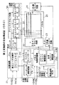
図18は、交流型PDP及びその駆動装置の構成図である。この図において、20は交流型PDP(以下「パネル」と略す)、21はアドレスドライバ、22はYスキャンドライバ、23はY共通ドライバ、24はX共通ドライバ、25は制御回路、26はAPC回路である。
【0009】
制御回路25は、表示データ制御部25aとパネル駆動制御部25bとを含み、表示データ制御部25aは、外部から与えられる表示データ(DATA)をフレームメモリ25cに一時記憶するとともに、このフレームメモリ25c内のデータに対して所定の信号操作とタイミング処理を施してアドレスドライバ21に出力する。パネル駆動制御部25bは、スキャンドライバ制御部25dや共通ドライバ制御部25eを含み、外部から与えられる垂直同期信号(VSYNC)及び水平同期信号(HSYNC)に基づいて各種タイミング信号を発生し、表示データ制御部25a、Yスキャンドライバ22、Y共通ドライバ23及びX共通ドライバ24などに供給する。
【0010】
アドレスドライバ21は、表示選択用高電圧電源Vaを用いてアドレスパルスを発生し、このアドレスパルスをパネル20のアドレス電極(A1 、A2 、……、Am )に選択的に印加する。また、Yスキャンドライバ22は、表示維持用高電圧電源Vsを用いてスキャンパルスを発生し、このスキャンパルスをパネル20のY電極(Y1 、Y2 、Y3 、……、Yn )に線順次で印加する。なお、これらのアドレスパルスやスキャンパルスは、1サブフレーム中の「アドレス期間」において発生する。
【0011】
Y共通ドライバ23は、表示維持用高電圧電源Vsを用いてサスティンパルスを発生し、1サブフレーム中の「維持放電期間」において、このサスティンパルスをパネル20のすべてのY電極に同時に印加し、X共通ドライバ24は、同じく表示維持用高電圧電源Vsを用いてサスティンパルス及び全面書込みパルスを発生し、1サブフレーム中の「リセット期間」において、この全面書込みパルスをパネル20のすべてのX電極に同時に印加するとともに、1サブフレーム中の「維持放電期間」において、このサスティンパルスを同X電極に同時に印加するものである。
(6)APC機能
PDPの消費電力は点灯画素数(表示率)により増減変化する。すなわち、維持放電期間で消費される最大の電力はすべての画素が点灯しているとき(表示率100%)であり、最小の電力はすべての画素が消灯しているとき(表示率0%)である。また、アドレス期間で消費される最大の電力は表示率50%で且つ表示パターンが表示セルごとに千鳥状に変化するような場合である。
【0012】
上限の消費電力Pmaxは、主に仕様要求で決まる。例えば、640×480画素の10インチ・バックライト付液晶パネルと同等の仕様要求であれば、Pmax=6W程度になる。上記のとおり、PDPの消費電力は表示率100%で最大になるため、この表示率100%のときの電力をPmaxに設定すれば簡単であるが、通常の映像表示における表示率は高々30%程度にすぎないから、通常動作範囲における電力とPmaxとの間に余裕がありすぎ、オーバースペックを否めない。
【0013】
そこで、表示率があらかじめ定められた基準の表示率(例えば通常動作範囲における表示率を若干上回る程度の表示率)を超えた場合に、サスティン周波数を下げて(言い換えれば上述の比率の“n”を小さくして)、PDPの電力消費をPmaxにリミットすることが行われている。
図19は、APC回路26の概略構成図である。表示維持用高電圧電源Vsは、電圧検出回路26aでその電圧値esを検出されると共に、電流検出回路26bでその電流値isを検出される。なお、isの検出は、典型的にはVsの経路上に抵抗素子を挿入してその両端電圧を測定すればよい。es及びisは、それぞれA/D変換器26c、26dでディジタルデータに変換された後、マイクロプロセッサ26eで電力値Psに換算演算(Ps=es×is)されると共に、このPsと基準電力(上述のPmaxに相当する)との比較判定が行われる。すなわち、PsがPmaxを超えている場合には、サスティン周波数を下げるための制御データが出力されるようになっており(図18参照)、実際の消費電力(Ps)を基準電力(Pmax)でリミットできる。
【0014】
【発明が解決しようとする課題】
ところで、かかる従来技術の不都合は、ドライバ類、中でもアドレスドライバ21の発熱対策が不十分な点にある。アドレスドライバ21の発熱は電力消費量、したがって画像の精細度に応じて増大する。また、表示パターンによっても大きく変化する。実際上640×480画素程度の精細度であれば、基板からの放熱で十分な熱収支を得られるが、それ以上の精細度(例えば800×600画素や1024×768画素)になると、もはや基板からの放熱だけでは不十分で、場合によってはアドレスドライバ21の熱破損を引き起こしかねない。また、表示パターンによっては特定のアドレスドライバが大きく発熱することがあり、この場合、トータルの電力消費が少ないにも拘らずその特定のアドレスドライバが熱破損することもある。
【0015】
この防止策は、▲1▼Pmaxを下げるか、▲2▼放熱フィンや冷却ファンを装着するしかない。しかしながら、▲1▼は起動直後のようにそれほど温度が上昇していない場合でもサスティン周波数の低下による画質劣化を否めないし、▲2▼は設置スペースや騒音の問題を生じるうえ、そもそも冷却ファンの電力を余分に必要とするという致命的な問題がある。さらに、従来技術は、特定のアドレスドライバの発熱を検出できないという問題点もある。
【0016】
そこで、本発明は、低中温状態での画質劣化を防止し、さらに設置スペースや騒音問題を招くことなく、しかも余分な電力も必要としない発熱対策を提供することを目的とする。
【0017】
【課題を解決するための手段】
請求項1に係る発明は、表示パネル上にマトリクス状に配列された画素を駆動するドライバを備える平面表示装置の駆動回路において、前記ドライバの温度を検出する温度検出手段と、該温度検出手段によって検出された温度が基準温度を超えているか否かを判定する判定手段と、該判定手段により、検出された温度が前記基準温度を超えていると判定された場合に、一部のサブフレームの動作を停止させる、或いは全ラインの表示をインターレス表示に切り替える、の少なくともいずれか一方を行う制御手段と、を備えたことを特徴とする。
【0018】
請求項1に係る発明では、ドライバの温度が基準温度を超えない限り、制御手段が動作しないため、基準温度以下での画質劣化が防止される。また、ドライバの温度が基準温度相当の温度でリミットされるため、基準温度を適正化しておけば、冷却ファンはもとより大型の放熱フィンも必要とせず、設置スペースや騒音問題を招かないうえ、余分な電力も必要としない。
【0019】
【発明の実施の形態】
以下、本発明の実施例を図面に基づいて説明する。
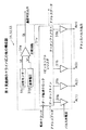
図1〜図4は、本発明に係る平面表示装置の駆動回路における第1実施例を示す図であり、サブフレーム方式の交流型PDPへの適用例である。なお、従来例(図18)と共通する構成要素には同一の符号を付してある。
【0020】
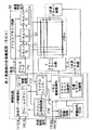
図1において、アドレスドライバ回路30は複数個(図では便宜的に3個)のドライバIC31〜33で構成(図2参照)されており、それぞれのドライバICの出力数をN、ドライバICの個数をMとすれば、このアドレスドライバ回路30は最大でN×M本のアドレスバスライン(すなわちN×M個の水平方向の画素)を持つ表示パネル20を駆動できる。後述するように、それぞれのドライバIC31〜33は温度判定出力を有しており、何れか一つのドライバICの温度判定出力がアクティブ(真)になると、制御回路25のマイクロコントローラ25fで“所定の制御ルーチン”が起動されるようになっている。“所定の制御ルーチン”とは、要するに、ドライバIC31〜33の温度上昇の要因となる物理量を操作する制御であり、特に限定しないが、本実施例の場合、パルス電源制御回路25gを制御してアドレス期間におけるアドレス電極駆動波形(例えばアドレスパルス;図17の符号14参照)のレベルを下げるという操作である。
【0021】
図3はドライバIC31〜33(以下、31で代表)に共通の構成図である。シフトレジスタ31aや出力バッファ(パルスアンプ)31bは従来のドライバICにも設けられている構成要素であるが、温度センサ31c、基準電圧31d、比較回路31e及び論理回路31fは本実施例に特有の構成要素である。すなわち、温度センサ31cはドライバIC31の基板温度若しくはパッケージ温度に応じた電圧Vtを発生するものであり、比較回路31eはVtと基準電圧Vrとを比較してVt>Vrのときにアクティブとなる信号Stを出力して論理回路31fの一入力に加えるものであり、論理回路31fは二つの入力の何れか一方又は両方がアクティブになったときにアクティブとなる信号(温度判定出力)を出力するものである。1段目のドライバIC31の温度判定出力は2段目のドライバIC32の論理回路32fの他入力に加えられており、また、2段目のドライバIC32の温度判定出力は3段目のドライバIC33の論理回路33fの他入力に加えられており、3段目のドライバIC33の温度判定出力は制御回路25のマイクロコントローラ25fに加えられている。すなわち、各ドライバICの温度判定出力がシリーズに接続され、一つでもアクティブになると、マイクロコントローラ25fに加えられる温度判定出力がアクティブになるようになっている。
【0022】
なお、図4に示すように、比較回路31eの出力(St)をそのドライバICの温度判定出力として取り出してもよい。この場合、各ドライバICからの温度判定出力のオア論理を取るための論理回路を別途設ければよい。
以上の構成において、各ドライバIC31〜33の実際の温度は、それぞれに設けられた温度センサ31cで検出される。今、ドライバIC31の温度が上昇したと仮定すると、温度センサ31cから出力される電圧Vtの値も上昇し、Vt>Vrになると、そのドライバIC31の温度判定出力がアクティブになる。したがって、マイクロコントローラ25fは所定の処理ルーチンを起動し、アドレス期間におけるアドレス電極駆動波形(例えばアドレスパルス;図17の符号14参照)のレベルが下げられる結果、ドライバIC31の温度上昇の速度が遅くなり、又は温度上昇がストップし、若しくは温度が下降に転ずるという何れかの作用が得られる。これは、アドレス電極駆動波形のレベルを下げると、ドライバICの特に出力バッファの電力消費を抑制できるからであり、電力消費と発熱は密接な関係にあるからである。
【0023】
ところで、上記第1実施例にあっては、どのドライバICの温度が基準を超えているのか見分けが付かない。このため、きめ細かな制御を行えない点で改良の余地がある。
図5〜図14は、本発明に係る平面表示装置の駆動回路における第2実施例であり、きめ細かな制御を行えるように改良したものである。
【0024】
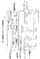
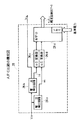
図5において、本第2実施例のドライバIC31は、比較回路31の出力(St)と前段のドライバICからの温度判定入力とを選択信号に従って切り換えるセレクタ回路31gと、セレクタ回路31hの出力を転送クロックに同期して保持すると共に温度判定出力として取り出す1ビットレジスタ回路31hとを有する点で第1実施例と相違する。
【0025】
例えば、i段目のドライバICのセレクタ回路31gを図示状態(Stの選択状態)に切り換えると共に、他のドライバICのセレクタ回路31gを図示と反対の状態に切り換えれば、全てのドライバICの1ビットレジスタ回路31hにi段目のドライバICの温度判定結果(St)を保持できる。したがって、選択信号を適宜に発生することにより、各ドライバICの温度判定結果(St)を順次に取り出すことができ、発熱状態のドライバICを特定できる。
【0026】
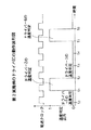
図6はその一例を示す図であり、この図では、時間t1〜t2、t5〜t6の間で温度判定出力がアクティブ(Hレベル)になっている。t0〜t1、t1〜t2、………、t5〜t6を各ドライバICに対応させたとすると、t1〜t2は2番目のドライバIC、t5〜t6は6番目のドライバICに対応する。したがって、この図によれば、2番目と6番目のドライバICが発熱状態にある。この状態は、例えば、2番目と6番目のドライバが受け持つ表示エリアに千鳥パターンが表示された場合などに現れる。
【0027】
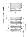
図7は、発熱状態にあるドライバICを特定できることを利用した、きめ細かな制御の一例であり、サブフレームのいくつかを停止するようにした例である。図7において、本実施例のドライバICは図5の構成を有しており、マイクロコントローラ25fはアドレスドライバ回路30からの特定のトライバICに対応した温度判定出力に応答してサブフレームのいくつかを停止するという所定の処理シーケースを実行する。
【0028】
図8は、連続する複数のフィールド(便宜的にフィールド1〜4)を示す図であり、この図では、フィールド2とフィールド3の第1及び第2サブフレームが動作停止となっている。言うまでもなく、停止状態のサブフレームでは、アドレスパルスやサスティンパルスなどが発生しないから、同サブフレーム期間でのドライバICは電力を消費せず、発熱を抑制できる。なお、図8では、第1及び第2サブフレーム、すなわち短期間側のサブフレームの動作を停止させているが、これは、画質の劣化を防止するためである。
【0029】
または、図9や図10に示すように、所定の処理シーケースでインターレース表示を行ってもよい。すなわち、図9のマイクロコントローラ25fは、アドレスドライバ回路30からの温度判定出力に応答してインターレース制御回路25iを制御し、奇数番目のラインと偶数番目のラインを二つのフィールドで表示するインターレース表示を行っている。
【0030】
図10は、インターレース表示の一例であり、この図では、フィールド1の終期にアクティブになった温度判定出力に応答して、フィールド2とフィールド3をインターレース表示にしている。インターレース表示ではフレーム周波数が実質的に1/2になるから、ドライバICの発熱を抑制できる。このため、図示の例では、フィールド3で温度判定出力がインアクティブとなり、続くフィールド4が全ライン表示に復帰している。
【0031】
図11は、上述のパルス電源制御回路25g、サブフレーム制御回路25h及びインターレース制御回路25iの併用例であり、マイクロコントローラ25fでアドレス電極駆動波形の低下操作、サブフレームのいくつかを動作停止させる操作、及びインターレース表示操作の一つ若しくはこれらの組み合わせを実行できるようにした例である。
【0032】
または、図12に示すように、パルス電源制御回路25gで各ドライバIC31〜33ごとのパルス電源を発生できるようにし、各ドライバIC31〜33ごとのパルス電源を個別に制御するようにしてもよい。
あるいは、図13に示すように、アドレスドライバ回路30に与えるアドレスデータ(表示データに相当)の下位ビットのいくつかを0に固定するためのデータ制御回路25jを設けてもよい。
【0033】
すなわち、図14に示すように、発熱状態にあるドライバIC(図では2番目のドライバICと6番目のドライバIC)に与える下位アドレスデータを0に固定すれば、当該ドライバICは非動作状態になるから、発熱を抑制できる。
【0034】
【発明の効果】
本発明によれば、低中温状態での画質劣化を防止し、さらに設置スペースや騒音問題を招かず、しかも余分な電力も必要としない発熱対策を提供でき、特にPDPの高画質化に貢献することができる。
【図面の簡単な説明】
【図1】第1実施例の全体構成図である。
【図2】第1実施例のアドレスドライバ回路の構成図である。
【図3】第1実施例のドライバICの構成図である。
【図4】第1実施例のドライバICの他の構成図である。
【図5】第2実施例のドライバICの構成図である。
【図6】第2実施例のドライバICの動作波形図である。
【図7】第2実施例の全体構成図(その1)である。
【図8】第2実施例のサブフレーム操作概念図である。
【図9】第2実施例の全体構成図(その2)である。
【図10】第2実施例のインターレース表示操作概念図である。
【図11】第2実施例の制御回路の他の構成図である。
【図12】第2実施例の全体構成図(その3)である。
【図13】第2実施例の全体構成図(その4)である。
【図14】第2実施例のアドレスデータ操作概念図である。
【図15】3電極型PDPの断面構造図である。
【図16】サブフレーム方式のフレーム構成図である。
【図17】1サブフレームの波形タイミング図である。
【図18】交流型PDP及びその駆動装置の概略構成図である。
【図19】APC回路の構成図である。
【符号の説明】
20:表示パネル
25f:マイクロコントローラ(制御手段)
31〜33:ドライバIC(ドライバ)
31c:温度センサ(温度検出手段)
31d:基準電圧(基準温度)
31e:比較回路(判定手段)[0001]
BACKGROUND OF THE INVENTION
The present invention relates to a driving circuit for a flat display device such as a plasma display panel, a TFT liquid crystal display panel, and an EL display panel, and more particularly to a driving circuit for a high-quality flat display device.
To improve the image quality of flat display devices such as plasma display panels, TFT liquid crystal display panels, and EL display panels, it is effective to increase the number of pixels and the frame frequency. Therefore, there is a demand for a technology that can achieve high image quality without impairing power saving.
[0002]
The driver for driving the display panel is dominant in the power consumption of the flat display device. In particular, a driver on the data side, for example, a data driver for driving a data bus line of a display panel in a TFT liquid crystal display, and an address driver for driving an address bus line of a display panel in a plasma display panel (hereinafter “PDP”) Power consumption is large. The driver on the data side has output buffers for the number of pixels that make up one line, but the power consumption of each output buffer is large, and the number of buffers tends to increase as the image quality improves. In addition, in a PDP that employs a driving method called a subframe method, assuming that the number of subframes is A, the buffer operates A times in one frame, and the frame frequency is substantially set to A. This is because, as a result of doubling, the power is increased A times by simple calculation.
[0003]
[Prior art]
As a technique for achieving both high image quality and power saving of the PDP in the flat display device, a function called APC (auto power control) is known.
(1) PDP cell structure and its driving principle There are two types of PDP basic cell structure: DC type with electrodes exposed to the discharge cell and AC type with electrodes covered with an insulating layer. On the other hand, the mainstream is the latter AC type. Further, the AC type PDP is also a two-electrode type in which an anode and a cathode are provided on each of two substrates, and an anode and a cathode are provided on one substrate and a third electrode (a so-called address electrode; A electrode) is provided on the other substrate. In particular, in the case of a color PDP, the three-electrode type is used because it can prevent deterioration of the phosphor. The positive / negative of the anode and cathode of the AC type PDP is determined by the polarity of the applied voltage, and depending on the driving method, there is also polarity reversal. Therefore, generally, the X electrode and the coordinate electrode (X, Y) of the panel are attached. It is called a Y electrode.
[0004]
FIG. 15 is a sectional view of a three-electrode type PDP, wherein 1, 2 are glass substrates, 3 is an A electrode, 4 is an X electrode, 5 is a Y electrode, 6 is a phosphor, 7 is an insulating film, and 8 is a dielectric.
[0005]
FIG. 16 is a conceptual diagram of a subframe frame structure. One frame is composed of a plurality of (eight in the figure) subframes SF1 to SF8. Each subframe is composed of three periods, that is, a “reset period”, an “address period”, and a “sustain discharge period”, and the lengths of the first two periods are the same, but the sustain discharge periods t1 to t8 are in the above ratio. It is different as follows. L1, L2,..., Ln are horizontal scanning lines. In addition, the thick diagonal lines within the address period of each subframe schematically represent a state in which L1, L2,..., Ln are selected in a line sequential manner.
[0006]
FIG. 17 is a waveform timing chart of the address electrode, the X electrode, and the Y electrode in one subframe period. Note that the voltage value used in the following description is a convenience value and is not limited to this. In the reset period, first, in order to give a sufficient potential difference necessary for discharge while applying 0 V to all the Y electrodes, a positive pulse of about +110 V is applied to the address electrodes, and a positive voltage of about +330 V is applied to the X electrodes. A pulse 11 (also referred to as a full write pulse) is applied. As a result, discharge occurs in all cells. Next, when 0 V is applied to the address electrode and the X electrode to cause discharge in all the cells again, this discharge is terminated by self-neutralization without forming wall charges because the potential difference between the electrodes is zero. Then, so-called self-erasing discharge is performed.
[0007]
In the address period, while applying a
[0008]
In the sustain discharge period (also referred to as the sustain period), positive pulses 16 (sustain pulses) of about +180 V are alternately applied to the X electrode and the Y electrode, and wall charges are used to discharge between the X and Y electrodes (sustain discharge). ; See FIG. 15). The period of the
(2) Schematic configuration of PDP and its driving device FIG. 18 is a configuration diagram of an AC type PDP and its driving device. In this figure, 20 is an AC type PDP (hereinafter abbreviated as “panel”), 21 is an address driver, 22 is a Y scan driver, 23 is a Y common driver, 24 is an X common driver, 25 is a control circuit, and 26 is an APC circuit. It is.
[0009]
The
[0010]
The
[0011]
The Y
(6) The power consumption of the APC function PDP varies depending on the number of lighting pixels (display rate). That is, the maximum power consumed in the sustain discharge period is when all the pixels are turned on (display rate 100%), and the minimum power is when all the pixels are turned off (display rate 0%). It is. The maximum power consumed in the address period is when the display rate is 50% and the display pattern changes in a staggered manner for each display cell.
[0012]
The upper limit power consumption Pmax is mainly determined by specification requirements. For example, if the specification requirement is the same as that of a 640 × 480 pixel 10-inch backlit liquid crystal panel, Pmax = 6 W. As described above, since the power consumption of the PDP becomes maximum at a display rate of 100%, it is easy to set the power at this display rate of 100% to Pmax, but the display rate in normal video display is at most 30%. Therefore, there is too much room between power and Pmax in the normal operating range, and over spec cannot be denied.
[0013]
Therefore, when the display rate exceeds a predetermined reference display rate (for example, a display rate that is slightly higher than the display rate in the normal operation range), the sustain frequency is lowered (in other words, the above-mentioned ratio “n”). The power consumption of the PDP is limited to Pmax.
FIG. 19 is a schematic configuration diagram of the
[0014]
[Problems to be solved by the invention]
By the way, the disadvantage of the prior art is that the measures for heat generation of the drivers, especially the
[0015]
The only preventive measures are (1) lowering Pmax, or (2) installing heat radiating fins and cooling fans. However, (1) cannot deny image quality deterioration due to a decrease in sustain frequency even when the temperature is not so high as just after startup, and (2) causes problems of installation space and noise, and power of the cooling fan in the first place. There is a fatal problem that requires extra. Furthermore, the prior art has a problem that it cannot detect the heat generated by a specific address driver.
[0016]
SUMMARY OF THE INVENTION An object of the present invention is to provide a countermeasure against heat generation that prevents image quality deterioration in a low and medium temperature state, does not cause installation space and noise problems, and does not require extra power.
[0017]
[Means for Solving the Problems]
According to a first aspect of the present invention, in a driving circuit for a flat panel display device including a driver for driving pixels arranged in a matrix on a display panel, a temperature detecting means for detecting the temperature of the driver, and the temperature detecting means A determination unit that determines whether or not the detected temperature exceeds a reference temperature; and when the determination unit determines that the detected temperature exceeds the reference temperature, And control means for performing at least one of stopping the operation or switching the display of all lines to the interlaced display .
[0018]
In the invention according to
[0019]
DETAILED DESCRIPTION OF THE INVENTION
Embodiments of the present invention will be described below with reference to the drawings.
1 to 4 are diagrams showing a first embodiment of a driving circuit of a flat panel display device according to the present invention, which is an application example to a subframe type AC type PDP. In addition, the same code | symbol is attached | subjected to the component which is common in a prior art example (FIG. 18).
[0020]
In FIG. 1, the
[0021]
FIG. 3 is a configuration diagram common to the
[0022]
As shown in FIG. 4, the output (St) of the
In the above configuration, the actual temperature of each of the
[0023]
By the way, in the first embodiment, it is impossible to tell which driver IC temperature exceeds the reference. For this reason, there is room for improvement in that fine control cannot be performed.
5 to 14 show a second embodiment of the driving circuit of the flat panel display device according to the present invention, which is improved so that fine control can be performed.
[0024]
In FIG. 5, the
[0025]
For example, if the
[0026]
FIG. 6 is a diagram showing an example thereof. In this figure, the temperature determination output is active (H level) between times t1 and t2 and t5 to t6. If t0 to t1, t1 to t2,..., t5 to t6 correspond to each driver IC, t1 to t2 correspond to the second driver IC, and t5 to t6 correspond to the sixth driver IC. Therefore, according to this figure, the second and sixth driver ICs are in a heat generating state. This state appears, for example, when a staggered pattern is displayed in the display area handled by the second and sixth drivers.
[0027]
FIG. 7 is an example of fine control using the ability to specify a driver IC in a heat generation state, and is an example in which some of the subframes are stopped. 7, the driver IC of this embodiment has the configuration shown in FIG. 5, and the
[0028]
FIG. 8 is a diagram showing a plurality of consecutive fields (
[0029]
Alternatively, as shown in FIGS. 9 and 10, interlaced display may be performed in a predetermined processing case. That is, the
[0030]
FIG. 10 shows an example of interlaced display. In this figure,
[0031]
FIG. 11 is a combination example of the above-described pulse power
[0032]
Alternatively, as shown in FIG. 12, the pulse power
Alternatively, as shown in FIG. 13, a
[0033]
That is, as shown in FIG. 14, if the lower address data to be given to the driver ICs in the heat generation state (second driver IC and sixth driver IC in the figure) is fixed to 0, the driver IC is brought into a non-operational state Therefore, heat generation can be suppressed.
[0034]
【The invention's effect】
According to the present invention, it is possible to provide a heat generation countermeasure that prevents image quality deterioration in a low and medium temperature state, does not cause installation space and noise problems, and does not require extra power, and contributes particularly to improving the image quality of a PDP. be able to.
[Brief description of the drawings]
FIG. 1 is an overall configuration diagram of a first embodiment.
FIG. 2 is a configuration diagram of an address driver circuit according to the first embodiment;
FIG. 3 is a configuration diagram of a driver IC according to the first embodiment;
FIG. 4 is another configuration diagram of the driver IC of the first embodiment.
FIG. 5 is a configuration diagram of a driver IC according to a second embodiment;
FIG. 6 is an operation waveform diagram of the driver IC of the second embodiment.
FIG. 7 is an overall configuration diagram (No. 1) of a second embodiment.
FIG. 8 is a conceptual diagram of subframe operation according to the second embodiment.
FIG. 9 is an entire configuration diagram (No. 2) of the second embodiment;
FIG. 10 is a conceptual diagram of an interlace display operation according to the second embodiment.
FIG. 11 is another configuration diagram of the control circuit of the second embodiment.
FIG. 12 is an overall configuration diagram (part 3) of the second embodiment;
FIG. 13 is an overall configuration diagram (part 4) of the second embodiment;
FIG. 14 is a conceptual diagram of address data operation according to the second embodiment.
FIG. 15 is a sectional view of a three-electrode type PDP.
FIG. 16 is a frame configuration diagram of a subframe method.
FIG. 17 is a waveform timing chart of one subframe.
FIG. 18 is a schematic configuration diagram of an AC type PDP and its driving device.
FIG. 19 is a configuration diagram of an APC circuit.
[Explanation of symbols]
20:
31-33: Driver IC (driver)
31c: Temperature sensor (temperature detection means)
31d: Reference voltage (reference temperature)
31e: Comparison circuit (determination means)
Claims (1)
前記ドライバの温度を検出する温度検出手段と、
該温度検出手段によって検出された温度が基準温度を超えているか否かを判定する判定手段と、
該判定手段により、検出された温度が前記基準温度を超えていると判定された場合に、一部のサブフレームの動作を停止させる、或いは全ラインの表示をインターレス表示に切り替える、の少なくともいずれか一方を行う制御手段と、を備えたことを特徴とする平面表示装置の駆動回路。In a driving circuit of a flat display device including a driver for driving pixels arranged in a matrix on a display panel,
Temperature detecting means for detecting the temperature of the driver;
Determination means for determining whether or not the temperature detected by the temperature detection means exceeds a reference temperature;
When it is determined by the determining means that the detected temperature exceeds the reference temperature, at least one of stopping the operation of some subframes or switching the display of all lines to the interlaced display. driving circuit of the flat panel display and a control unit, comprising the to either perform one.
Priority Applications (1)
| Application Number | Priority Date | Filing Date | Title |
|---|---|---|---|
| JP19468897A JP3757345B2 (en) | 1997-07-22 | 1997-07-22 | Driving circuit for flat display device |
Applications Claiming Priority (1)
| Application Number | Priority Date | Filing Date | Title |
|---|---|---|---|
| JP19468897A JP3757345B2 (en) | 1997-07-22 | 1997-07-22 | Driving circuit for flat display device |
Related Child Applications (1)
| Application Number | Title | Priority Date | Filing Date |
|---|---|---|---|
| JP2005269799A Division JP2006039586A (en) | 2005-09-16 | 2005-09-16 | Plasma display device |
Publications (2)
| Publication Number | Publication Date |
|---|---|
| JPH1138930A JPH1138930A (en) | 1999-02-12 |
| JP3757345B2 true JP3757345B2 (en) | 2006-03-22 |
Family
ID=16328635
Family Applications (1)
| Application Number | Title | Priority Date | Filing Date |
|---|---|---|---|
| JP19468897A Expired - Fee Related JP3757345B2 (en) | 1997-07-22 | 1997-07-22 | Driving circuit for flat display device |
Country Status (1)
| Country | Link |
|---|---|
| JP (1) | JP3757345B2 (en) |
Families Citing this family (17)
| Publication number | Priority date | Publication date | Assignee | Title |
|---|---|---|---|---|
| JP4528449B2 (en) * | 2001-01-12 | 2010-08-18 | 日立プラズマディスプレイ株式会社 | Driving method and display device of plasma display panel |
| JP4667619B2 (en) * | 2001-02-27 | 2011-04-13 | パナソニック株式会社 | Plasma display device and driving method thereof |
| JP2003043991A (en) * | 2001-08-02 | 2003-02-14 | Fujitsu Hitachi Plasma Display Ltd | Plasma display device |
| KR100425482B1 (en) * | 2001-10-25 | 2004-03-30 | 엘지전자 주식회사 | Plasma display panel and driving method thereof |
| KR100480150B1 (en) * | 2001-11-28 | 2005-04-06 | 엘지전자 주식회사 | Method and apparatus for controlling data |
| WO2003075252A2 (en) * | 2002-03-06 | 2003-09-12 | Koninklijke Philips Electronics N.V. | Display panel with energy recovery system |
| KR20040023931A (en) * | 2002-09-12 | 2004-03-20 | 엘지전자 주식회사 | Driving method and apparatus of plasma display panel |
| KR100489877B1 (en) * | 2002-10-31 | 2005-05-17 | 엘지전자 주식회사 | Apparatus and method for driving plasma display panel |
| JP2004177557A (en) * | 2002-11-26 | 2004-06-24 | Mitsubishi Electric Corp | Driving method of matrix image display device, driving method of plasma display panel, and matrix image display device |
| KR100586997B1 (en) * | 2004-10-07 | 2006-06-08 | 삼성전자주식회사 | Driving Method for Display Panel And Control Method Thereof |
| JP4667079B2 (en) * | 2005-03-07 | 2011-04-06 | シャープ株式会社 | Display device |
| US20090231234A1 (en) * | 2005-06-27 | 2009-09-17 | Makoto Onozawa | Plasma display apparatus |
| WO2007086133A1 (en) * | 2006-01-27 | 2007-08-02 | Fujitsu Hitachi Plasma Display Limited | Plasma display apparatus |
| JPWO2008056397A1 (en) * | 2006-11-06 | 2010-02-25 | 日立プラズマディスプレイ株式会社 | Plasma display device |
| CN101548308B (en) * | 2007-01-15 | 2012-11-07 | 松下电器产业株式会社 | Plasma display device |
| JP5167683B2 (en) * | 2007-04-20 | 2013-03-21 | パナソニック株式会社 | Driving method of plasma display device |
| JP5245281B2 (en) * | 2007-04-20 | 2013-07-24 | パナソニック株式会社 | Driving method of plasma display device |
-
1997
- 1997-07-22 JP JP19468897A patent/JP3757345B2/en not_active Expired - Fee Related
Also Published As
| Publication number | Publication date |
|---|---|
| JPH1138930A (en) | 1999-02-12 |
Similar Documents
| Publication | Publication Date | Title |
|---|---|---|
| JP3757345B2 (en) | Driving circuit for flat display device | |
| JP4112647B2 (en) | Driving circuit for matrix display device | |
| KR100516344B1 (en) | Method for driving plasma display | |
| JPH10207426A (en) | Method of driving plasma display panel display device and drive controller therefor | |
| KR20000007601A (en) | Plasma display panel driving method and device thereof | |
| JPH09244575A (en) | Plasma display panel driving device | |
| JPH10207427A (en) | Driving method for plasma display panel display device and driving control device | |
| JP4257313B2 (en) | Plasma display panel and driving method thereof | |
| JP2002023694A (en) | Multigradation image display device which reduces power consumption during data writing | |
| JPH10319900A (en) | Driving method of plasma display device | |
| JP3675798B2 (en) | Driving circuit for plasma display device and driving method for plasma display device | |
| JP2000276105A (en) | Display device and driving device | |
| JPH10177365A (en) | Drive controller for plasma display panel display device | |
| EP1477959A2 (en) | Plasma display device | |
| KR100426187B1 (en) | Method and Apparatus for Driving Plasma Display Panel | |
| JP2005234305A (en) | Capacitive load driving circuit and its driving method, and plasma display device | |
| US20050264486A1 (en) | Plasma display panel and driving method thereof | |
| JP2006039586A (en) | Plasma display device | |
| KR19990017532A (en) | AC plasma display device and panel driving method | |
| US20090066679A1 (en) | Plasma display device | |
| KR100542212B1 (en) | Driving method of plasma display panel and apparatus thereof | |
| KR100425482B1 (en) | Plasma display panel and driving method thereof | |
| KR100581879B1 (en) | Controlling method of address voltage in plasma display panel | |
| KR100493620B1 (en) | Method and apparatus for dispersing sustaing current of plasma display panel | |
| KR100599646B1 (en) | Plasma display panel and abnormality detection method thereof |
Legal Events
| Date | Code | Title | Description |
|---|---|---|---|
| RD02 | Notification of acceptance of power of attorney |
Free format text: JAPANESE INTERMEDIATE CODE: A7422 Effective date: 20050527 |
|
| A977 | Report on retrieval |
Free format text: JAPANESE INTERMEDIATE CODE: A971007 Effective date: 20050624 |
|
| A131 | Notification of reasons for refusal |
Free format text: JAPANESE INTERMEDIATE CODE: A131 Effective date: 20050719 |
|
| A711 | Notification of change in applicant |
Free format text: JAPANESE INTERMEDIATE CODE: A711 Effective date: 20050720 |
|
| RD01 | Notification of change of attorney |
Free format text: JAPANESE INTERMEDIATE CODE: A7421 Effective date: 20050720 |
|
| A521 | Written amendment |
Free format text: JAPANESE INTERMEDIATE CODE: A523 Effective date: 20050920 |
|
| A711 | Notification of change in applicant |
Free format text: JAPANESE INTERMEDIATE CODE: A711 Effective date: 20050921 |
|
| A521 | Written amendment |
Free format text: JAPANESE INTERMEDIATE CODE: A523 Effective date: 20051206 |
|
| RD04 | Notification of resignation of power of attorney |
Free format text: JAPANESE INTERMEDIATE CODE: A7424 Effective date: 20051207 |
|
| TRDD | Decision of grant or rejection written | ||
| A01 | Written decision to grant a patent or to grant a registration (utility model) |
Free format text: JAPANESE INTERMEDIATE CODE: A01 Effective date: 20051213 |
|
| A61 | First payment of annual fees (during grant procedure) |
Free format text: JAPANESE INTERMEDIATE CODE: A61 Effective date: 20051214 |
|
| R150 | Certificate of patent or registration of utility model |
Free format text: JAPANESE INTERMEDIATE CODE: R150 |
|
| FPAY | Renewal fee payment (event date is renewal date of database) |
Free format text: PAYMENT UNTIL: 20090113 Year of fee payment: 3 |
|
| FPAY | Renewal fee payment (event date is renewal date of database) |
Free format text: PAYMENT UNTIL: 20100113 Year of fee payment: 4 |
|
| FPAY | Renewal fee payment (event date is renewal date of database) |
Free format text: PAYMENT UNTIL: 20110113 Year of fee payment: 5 |
|
| FPAY | Renewal fee payment (event date is renewal date of database) |
Free format text: PAYMENT UNTIL: 20110113 Year of fee payment: 5 |
|
| FPAY | Renewal fee payment (event date is renewal date of database) |
Free format text: PAYMENT UNTIL: 20120113 Year of fee payment: 6 |
|
| FPAY | Renewal fee payment (event date is renewal date of database) |
Free format text: PAYMENT UNTIL: 20130113 Year of fee payment: 7 |
|
| S131 | Request for trust registration of transfer of right |
Free format text: JAPANESE INTERMEDIATE CODE: R313135 |
|
| SZ03 | Written request for cancellation of trust registration |
Free format text: JAPANESE INTERMEDIATE CODE: R313Z03 |
|
| R350 | Written notification of registration of transfer |
Free format text: JAPANESE INTERMEDIATE CODE: R350 |
|
| S111 | Request for change of ownership or part of ownership |
Free format text: JAPANESE INTERMEDIATE CODE: R313113 |
|
| FPAY | Renewal fee payment (event date is renewal date of database) |
Free format text: PAYMENT UNTIL: 20140113 Year of fee payment: 8 |
|
| LAPS | Cancellation because of no payment of annual fees |