JP3740195B2 - Data processing device - Google Patents
Data processing device Download PDFInfo
- Publication number
- JP3740195B2 JP3740195B2 JP24087195A JP24087195A JP3740195B2 JP 3740195 B2 JP3740195 B2 JP 3740195B2 JP 24087195 A JP24087195 A JP 24087195A JP 24087195 A JP24087195 A JP 24087195A JP 3740195 B2 JP3740195 B2 JP 3740195B2
- Authority
- JP
- Japan
- Prior art keywords
- address
- logical
- size
- page
- tlb
- Prior art date
- Legal status (The legal status is an assumption and is not a legal conclusion. Google has not performed a legal analysis and makes no representation as to the accuracy of the status listed.)
- Expired - Fee Related
Links
Images


Classifications
-
- G—PHYSICS
- G06—COMPUTING; CALCULATING OR COUNTING
- G06F—ELECTRIC DIGITAL DATA PROCESSING
- G06F15/00—Digital computers in general; Data processing equipment in general
- G06F15/16—Combinations of two or more digital computers each having at least an arithmetic unit, a program unit and a register, e.g. for a simultaneous processing of several programs
-
- G—PHYSICS
- G06—COMPUTING; CALCULATING OR COUNTING
- G06F—ELECTRIC DIGITAL DATA PROCESSING
- G06F12/00—Accessing, addressing or allocating within memory systems or architectures
- G06F12/02—Addressing or allocation; Relocation
- G06F12/08—Addressing or allocation; Relocation in hierarchically structured memory systems, e.g. virtual memory systems
- G06F12/10—Address translation
- G06F12/1027—Address translation using associative or pseudo-associative address translation means, e.g. translation look-aside buffer [TLB]
- G06F12/1036—Address translation using associative or pseudo-associative address translation means, e.g. translation look-aside buffer [TLB] for multiple virtual address spaces, e.g. segmentation
-
- G—PHYSICS
- G06—COMPUTING; CALCULATING OR COUNTING
- G06F—ELECTRIC DIGITAL DATA PROCESSING
- G06F12/00—Accessing, addressing or allocating within memory systems or architectures
- G06F12/02—Addressing or allocation; Relocation
- G06F12/08—Addressing or allocation; Relocation in hierarchically structured memory systems, e.g. virtual memory systems
- G06F12/10—Address translation
- G06F12/1027—Address translation using associative or pseudo-associative address translation means, e.g. translation look-aside buffer [TLB]
-
- G—PHYSICS
- G06—COMPUTING; CALCULATING OR COUNTING
- G06F—ELECTRIC DIGITAL DATA PROCESSING
- G06F2212/00—Indexing scheme relating to accessing, addressing or allocation within memory systems or architectures
- G06F2212/65—Details of virtual memory and virtual address translation
- G06F2212/652—Page size control
-
- Y—GENERAL TAGGING OF NEW TECHNOLOGICAL DEVELOPMENTS; GENERAL TAGGING OF CROSS-SECTIONAL TECHNOLOGIES SPANNING OVER SEVERAL SECTIONS OF THE IPC; TECHNICAL SUBJECTS COVERED BY FORMER USPC CROSS-REFERENCE ART COLLECTIONS [XRACs] AND DIGESTS
- Y02—TECHNOLOGIES OR APPLICATIONS FOR MITIGATION OR ADAPTATION AGAINST CLIMATE CHANGE
- Y02D—CLIMATE CHANGE MITIGATION TECHNOLOGIES IN INFORMATION AND COMMUNICATION TECHNOLOGIES [ICT], I.E. INFORMATION AND COMMUNICATION TECHNOLOGIES AIMING AT THE REDUCTION OF THEIR OWN ENERGY USE
- Y02D10/00—Energy efficient computing, e.g. low power processors, power management or thermal management
Landscapes
- Engineering & Computer Science (AREA)
- Theoretical Computer Science (AREA)
- Physics & Mathematics (AREA)
- General Engineering & Computer Science (AREA)
- General Physics & Mathematics (AREA)
- Computer Hardware Design (AREA)
- Software Systems (AREA)
- Memory System Of A Hierarchy Structure (AREA)
Abstract
Description
【0001】
【産業上の利用分野】
本発明は、アドレス変換機構を有するデータ処理装置に関し、特に、アドレス変換機構として、セットアソシアティブ方式のキャッシュメモリを利用したデータ処理装置に係り、更に述べるならば、そのアドレス変換手法の多様化を企図したものであり、例えばマイクロコンピュータに適用して有効な技術に関する。
【0002】
【従来の技術】
ユーザが実メモリを意識せずに、オペレーティングシステム(以下OSとも記す)がメモリ管理を行う分野では、データ処理装置がアドレス変換機構をサポートする必要がある。アドレス変換機構とは、仮想記憶を実現するために、中央処理装置(CPU)により形成された論理アドレスを物理アドレスに変換する機構である。このアドレス変換機構を高速に実行するために、論理アドレスと物理アドレスとの変換対を保持するアドレス変換バッファ(Translation lookaside buffer、以下単にTLBとも記す)を、中央処理装置とともにデータ処理装置に内蔵する技術が採用される。アドレス変換バッファは、例えば、最近使用された論理アドレスと物理アドレスとの変換対を保持する連想記憶構造のバッファメモリとして構成される。連想記憶構造のバッファメモリとしては、各メモリセルに比較のための回路構成を備えたCAM(Content Addressable Memory)から成るフルアソシアティブメモリ、汎用のランダムアクセスメモリを利用して比較的高いヒット率を実現できるセットアソシアティブ形式の連想メモリなどを利用することができる。尚、連想記憶形式のアドレス変換バッファについて記載された文献の例としては昭和61年2月10日に株式会社培風館から発行された「超高速MOSデバイス」第287頁及び第288頁がある。
【0003】
【発明が解決しようとする課題】
本発明者は、このようなアドレス変換バッファにつき、ユーザの要求仕様に応えることができ、良好な使い勝手を実現するという点について検討したところ以下のような問題点を見出した。
【0004】
(1)仮想記憶をサポートするアドレス変換機構においては、論理アドレス空間を論理ページと呼ばれる単位に分割して、そのページ単位に物理アドレスへのアドレス変換を行う。一方、システムに、実際に実装される実メモリ(物理メモリ)の全記憶容量が少ないような場合には、論理ページのサイズを比較的小さくして、各プロセスによるメモリの利用効率を向上させたいという要求などがある。例えば、実行されるべきタスクが、比較的小さなサイズのプログラムで構成される場合、そのタスクに割り当てられる論理ページのサイズが比較的大きいと、これに対応して、そのタスクを実行するための物理ページのサイズも比較的大きくなってしまう。そのため、必要以上の記憶空間が、タスクに割り当てられることになり、メモリの利用効率が低下する。特に、実メモリの記憶容量が比較的小さい場合には、論理ページのサイズを小さくして、実メモリの利用効率が低下するのを防ぐことが望まれる。このような要求に、適宜対応できるようにするには、論理ページのサイズを可変にすることが望ましい。ところが、論理ページのサイズを可変にすると、一定の論理空間において論理ページを規定するための情報のビット数が変化される。その結果、アドレス変換バッファから情報を連想的に検索するための比較対象情報のビット数やビット位置が、論理ページサイズによって変化されなければならない。これに対処するために、アドレス変換バッファにCAMから成るフルアソシアティブ形式を採用することが考えられる。このようにすれば、各メモリセルが比較回路を備えていることから特別な考慮を要することなく、比較的簡単に、論理ページの可変化を実現できる。しかしながら、各メモリセルが比較回路を備えているためセットアソシアティブ形式のアドレス変換バッファに比べてチップ専有面積と消費電力が共に倍増するという欠点が有る。
【0005】
(2)セットアソシアティブ形式のアドレス変換バッファにおいては、複数セット存在するバンクの数、即ちウェイ数を増やせば一つのインデックスアドレスに対して保持できるエントリ数を増やして、ヒット率を向上させることができる。例えば4ウェイ・セットアソシアティブ形式の場合には、一つのインデックスアドレスに対して最大4個のエントリを保持できる。しかしながら、複数のプロセスの夫々が論理空間の全域にわたるアドレス変換情報を有し、プロセス番号によって論理アドレスを修飾或いは拡張する多重仮想記憶を行う場合、比較的多くのプロセスが並列的に起動されると、夫々のプロセスが同一論理ページを利用する頻度が多くなる。各々のプロセスは、プロセス番号が互いに異なるため、一つのインデックスアドレスによって指示されるところの互いに異なるエントリに保持されることになる。そのため、プロセスの数が、ウエイの数を越えると、セットアソシアティブ形式であっても、ヒット率は相対的に低下することになる。したがって、多重仮想記憶において多くのプロセスが並列的に起動される利用形態においては、ヒット率の低下を抑えることができるように、その利用形態に応じてインデックス方法を選択可能にすることの必要性が見出された。
【0006】
(3)目的とする変換対がアドレス変換バッファに格納されていない場合には、当該キャッシュミスに係る変換対(所望の変換対)が新たなエントリとしてアドレス変換バッファに追加される。このとき、インデックスされたエントリにおける変換対の全てが有効な変換対である場合には、変換対の置き換えが行われる。この置き換えのアルゴリズム(リプレースメントアルゴリズム)には、ランダム、最初にロードされたものからリプレースするFIFO、又は最後に参照されたものからリプレースするLRU(Least Recentry Used)などがある。しかしながら、リプレースメントアルゴリズムを固定化した場合には、データ処理の都合上、常に特定の変換対をアドレス変換バッファにエントリとして格納しておきたいという要求や、特定のアドレス変換対をリプレース対象にしたくないという要求には一切答えることができない。
【0007】
(4)仮想記憶の形式には上記多重仮想記憶の他に、複数のプロセスに論理アドレス空間の一部が排他的に割り当てられる単一仮想記憶がある。使い勝手を向上させるという点においては、これらの双方をサポートできるようにすることが望ましい。
【0008】
本発明の目的は、ユーザの要求仕様に応えることができて使い勝手の良好なアドレス変換機構を備えたデータ処理装置を実現することにある。
【0009】
本発明の目的を、更に詳述すれば、次の通りである。チップ専有面積と電力消費量を増大させることなく複数のページサイズをサポートできるアドレス変換機構を備えたデータ処理装置を提供すること。
【0010】
複数のインデックス方法をサポートし、それらからインデックス方法を選択できるアドレス変換機構を備えたデータ処理装置を提供すること。
【0011】
アドレス変換対のリプレース対象に自由度を持たせることができるアドレス変換機構を備えたデータ処理装置を提供すること。
【0012】
また、サポートできる仮想記憶形式についても自由度を持たせることができるアドレス変換機構を備えたデータ処理装置を提供すること。
【0013】
本発明の前記並びにその他の目的と新規な特徴は本明細書の記述及び添付図面から明らかになるであろう。
【0014】
【課題を解決するための手段】
本願において開示される発明のうち代表的なものの概要を簡単に説明すれば下記の通りである。
【0015】
《複数ページサイズをサポート》 仮想記憶をサポートするデータ処理装置は、論理アドレス空間を論理ページと呼ばれる単位に分割して、そのページ単位で、論理アドレスを物理アドレスへ変換(アドレス変換)する。このデータ処理装置では、図1に例示されるように、その論理ページのサイズが、ページ毎に可変とされる。それぞれサイズが可変な複数の論理ページに対して、アドレス変換バッファのようなバッファメモリ1は、共通に利用される。このバッファメモリ1としては、論理ページ番号VPNとそれに対応する物理ページ番号PPNとを含むところの対応情報を、記憶するための記憶領域を夫々供え、共通のインデックスアドレス2によってアクセスされる複数バンク11〜14を持つセットアソシアティブ方式のキャッシュメモリが使われる。
【0016】
サポートする論理ページの最大サイズは最小サイズの2のべき乗数倍(2のN乗倍)にされ、セットアソシアティブ方式のバッファメモリのバンクの数がその2のべき乗数(2のN乗数)以上とされる。更に詳しくは、図1に例示されるように、全体で4GB(ギガバイト)とされる論理アドレス空間(ビット0〜ビット31の論理アドレスで指定される)において、論理ページのサイズは、4KB(キロバイト)と1KBの2種類とされる。この場合、バッファメモリ1のバンクの数は4個とされ、バッファメモリ1は4ウェイ・セットアソシアティブ形式のキャッシュメモリとして構成される。論理ページサイズが4KBのとき、論理アドレスのオフセットは、論理アドレスのビット0〜ビット11とされ、論理ページ番号vpnは、論理アドレスのビット12〜ビット31とされる。論理ページサイズが1KBのとき、論理アドレスのオフセットは、論理アドレスのビット0〜ビット9とされ、論理ページ番号vpnは、論理アドレスのビット10〜ビット31とされる。尚、本明細書において小文字で示されるvpn,ppn,asidは、アクセスに利用される論理ページ番号、物理ページ番号、プロセス番号とされ、大文字で示されるバッファメモリ(アドレス変換バッファ)のエントリもしくはページテーブルエントリとしての論理ページ番号VPN、物理ページ番号PPN、プロセス番号ASIDとは区別される。
【0017】
上記アドレス変換バッファにおいて、バッファメモリ1に対するインデックスアドレスの指定方法は、論理ページのサイズが4KBと1KBの双方において共通化され、最大ページサイズの論理ページアドレスにおける最下位から所定の複数ビットがインデックスアドレスとして与えられる。上記図1の例に従えば、全部で32ビットの論理アドレスにおけるビット12〜ビット16の5ビットを用いてバッファメモリ1がインデックスされる。インデックスアドレスは5ビットであるから、1バンク当たり最大32個のエントリを保有できる。図1の例のように、4個のバンクを持つ場合には、一つのインデックスアドレスにつき、最大4個のエントリを保有できる。上記インデックスアドレスは、ページサイズが4KBの場合には、当該論理ページ番号vpnの最下位から5ビット(ビット12〜16)とされるので、ページサイズ4KBのときは、任意の論理ページ番号のエントリを、各バンクに最大32個(全体で128エントリ)保有することができる。一方、ページサイズが1KBの場合には、当該論理ページ番号vpnの最下位から2ビット(ビット10,11)がインデックスに利用されないことになる。すなわち、論理ページサイズが1KBであって、一つのバンクに対するインデックスだけを考えると、インデックスされたエントリは、インデックスに利用されない2ビット(ビット10,11)によって更にその中から1個が選ばれるべき4個の論理ページ番号の内の何れか一つとされる。したがって、バンクの数が1個しか存在しない場合には、連続する4個の論理ページの内の1個しかエントリとして保有することができない。この点においては、論理ページの最大サイズ(4KB)が、最小サイズ(1KB)の2の2乗倍とされ、バンク数も2の2乗個(4個)設けることにより、バッファメモリ(アドレス変換バッファ)全体としては4KBページサイズとほぼ同様に、任意の論理ページ番号のエントリを、全体で128個保有することができる。但し、一つのバンクに保有できるエントリの論理ページ番号は4KB毎という制約を受ける。この制限は、アドレス変換バッファの保有するエントリの論理ページ番号が連続的であれば、ヒット(TLBヒット)率には何等影響を与えない。分散的である場合にはある程度ヒット率に影響を受ける。この場合でも、1KBの論理ページを2KB毎にアドレスマッピングすればその影響を小さくでき、4KB毎にアドレスマッピングすれば全く影響を受けないようにすることができる。
【0018】
TLBヒット/ミスを判定するために、各バンク11〜14に設けられた比較手段15においてヒット判定に反映されるべきアドレス比較のビット数は、論理ページサイズに応じて変化されなければならない。図1の例に従えば、論理ページサイズが1KBの場合には、論理ページサイズが4KBの場合に比べて、論理アドレスのビット10及びビット11も比較対象としなければならない。バッファメモリ1は、そのような比較対象のビット数を全てカバーできるように、論理ページ番号と物理ページ番号との対応情報(変換対)を記憶する領域のビット数が設定されている。バッファメモリ1においては、各変換対にそれがサポートする論理ページサイズを示すフィールドが設けられており、そのフィールドの値(サイズビット)SZに応じてヒット判定のためのアドレス比較のビット数が変化される。比較ビット数が変化される対象は、論理アドレスの論理ページ番号と、バッファメモリ内の変換対に含まれる論理ページ番号の双方とされる。hit1〜hit4は各バンク11〜14におけるヒット判定結果を通知するためのヒット信号であり、それらに基づいてTLBヒット/ミスが判定される。
【0019】
《複数のインデックス方法をサポート》 仮想記憶をサポートするデータ処理装置は、論理ページ番号と物理ページ番号との対応情報を記憶するための記憶領域を夫々有し、夫々が共通のインデックスアドレスによってアクセスされる複数バンクを持つセットアソシアティブ方式のキャッシュメモリによって構成されたバッファメモリを供える。そして、そのバッファメモリに対するインデックスアドレスの生成手法を可変とする手段を有する。例えば、複数のプロセスが存在し、夫々のプロセスが夫々のアドレス変換情報を有し、プロセス番号によってそれぞれのプロセスが区別される多重仮想記憶をサポートする場合、バッファメモリからエントリをインデックスするためのアドレス指定方法として、図2に例示されるように論理アドレスの一部(ビット12〜16)のみをデコードする手法と、図3に示されるようにその論理アドレスの一部(ビット12〜16)を現在のプロセス番号(asid)の一部によって修飾(XOR=排他的論理和)した結果をデコードする手法とを、レジスタMMUCR.IXの論理値にしたがって指示するようにできる。尚、図3,図2において、バッファメモリ1内の変換対に含まれる論理ページ番号VPNの情報はインデックスに利用されるvpn(16−12)に対応されるものが除かれて、VPN(31−17),VPN(11−10)として図示されている。ここで、vpn(16−12)の表記は論理アドレスのビット12〜ビット16を含む論理ページ番号の情報であることを意味する。VPN(31−17)の表記は論理アドレスのビット17〜ビット31に対応されるバッファメモリのエントリとしての論理ページ番号の情報であることを意味する。
【0020】
《リプレースの自由度》 仮想記憶をサポートするデータ処理装置は、図4に例示されるように、論理ページ番号VPNと物理ページ番号PPNとの対応情報を記憶するための記憶領域を夫々供え、夫々のインデックスアドレスが共通化された複数バンク11〜14を持つ4ウェイ・セットアソシアティブ方式のキャッシュメモリから成るバッファメモリ1を有し、キャッシュミスなどの発生によって、これらの複数バンクの中から記憶情報を置換すべき場合に、当該置換されるべきセットは、中央処理装置によるソフトウェアの実行によって任意に指定可能にされる。例えばMMUCR.RCは、上記バンクを任意に指定するための2ビットの情報が設定されるレジスタである。これに設定された値がデコーダ17によって解読されることにより4個のバンク11〜14の中から一つを選ぶ信号(BSK1〜BSL4)が形成される。これにより、4個のバンク11〜14の内、上記選択信号によって指定された1個のバンクであって、インデックスアドレス2で指定された1つのエントリが置換対象とされる。このレジスタMMUCR内のビットMMUCR.RCに対する値の設定がハードウェア手段によって行われるとき、当該ハードウェア手段によるバンクの指定は上記中央処理装置(CPU)によるソフトウェアの実行によって任意に変更可能にされる。
【0021】
上記ハードウェア手段は、図4に例示されるように、MMUCR.RCをランダムカウンタのような計数手段として備え、その計数手段のビット数の2のべき乗数が、上記バッファメモリ1のバンクの数(=4)と一致される。上記ハードウェア手段に含まれる制御回路CTRLは、バッファメモリ1に対する記憶情報の置換が必要になった場合、上記計数手段を1インクリメントし、何れのバンクの、インデックスされた記憶領域にも有効なデータが保持されている(インデックスされた各バンクの各エントリが、有効を示す”1”のバリッドビットVを有する)場合には、そのインクリメントされた結果を置換すべきバンク番号とする。これに対して、何れかのバンク内で、インデックスされた記憶領域に、有効なデータが保持されていない(インデックスされた何れかのエントリが、無効を示す”0”のバリッドビットVを有する)場合には、有効なデータを保持していないエントリを含むバンクの番号を計数手段にセットし、且つセットされた番号のバンクを置換すべきバンクとする。このような一定の規則に従って、置換すべきバンクの指定が行われる。このとき、上記計数手段の各ビットは、中央処理装置により実行されるソフトウェアによって、任意の値へ変更することが可能な対象とされている。
【0022】
《単一仮想記憶と多重仮想記憶のサポート》 仮想記憶をサポートするデータ処理装置は、論理アドレス空間を論理ページと呼ばれる単位に分割して、そのページ単位で、論理アドレスを物理アドレスへアドレス変換を行うためのアドレス変換機構を備える。このアドレス変換機構は、複数のプロセスの夫々が論理空間の全域にわたるアドレス変換情報を有するとき、プロセス番号(asid)によって論理アドレスを修飾或いは拡張する多重仮想記憶と、複数のプロセスに論理アドレス空間の一部が排他的に割り当てられ、夫々のプロセスがそれに割り当てられた論理アドレス空間のアドレス変換情報を有するとき、プロセス番号(asid)によって論理アドレスを修飾或いは拡張しない単一仮想記憶とを有し、該多重仮想記憶と該単一仮想記憶とを選択することが可能にされている。したがって図5に例示されるようにバッファメモリ内の各エントリには、論理ページ番号VPNと物理ページ番号PPNの変換対に加え、プロセス番号ASIDのフィールドが設けられている。このフィールドの内容は、単一仮想記憶か多重仮想記憶かで、その処理内容が相違されることになる。あるTLBエントリに含まれるプロセス番号に対応される論理ページが、他のプロセスと共有不可能とされているとき、多重仮想記憶においては、プロセス番号ASIDのフィールドの内容はバッファメモリに対する検索のヒット/ミス(TLBヒット/TLBミス)の判定に用いられる。即ち、この場合には、バッファメモリに格納されているエントリの論理ページ番号VPNの情報が、論理ページアドレスvpnの情報に一致すると共に、当該エントリのプロセス番号ASIDが現在のプロセスの番号asidに一致していなければTLBヒットとはされない。単一仮想記憶においては、プロセス番号ASIDのフールドの内容はメモリ保護情報として使用される。即ち、この場合には、プロセス番号の相違によってTLBミスが発生したとき、ソフトウェアによってTLBミスの原因がプロセス番号の相違によるものか、論理ページアドレスの相違によるものかが判別され、プロセス番号の相違による場合には、プロテクションエラーとして処理される。上記単一仮想記憶か多重仮想記憶かは、図6に例示されるレジスタMMUCRのビットMMUCR.SVの値によって指示される。このビットMMUCR.SVの値は、中央処理装置によって実行されるソフトウェアによって、任意に設定することができる。
【0023】
【作用】
複数ページサイズを選択的にサポートするデータ処理装置は、システムに実装される実メモリの全記憶容量が少ないような場合に、論理ページのサイズを比較的小さくして、各プロセスによるメモリの利用効率を向上させたいという要求にも容易に対応できる。このとき、最大論理ページサイズを最小サイズの2のべき乗数倍にし、セットアソシアティブ方式のバッファメモリのバンクの数をその2のべき乗数以上にすることは、インデックスアドレスの指定手法を最大論理ページサイズのものに統一しても、選ばれる論理ページのサイズに拘わらず、原理的には、どの論理ページ番号のエントリについても、同じ数だけエントリをバッファメモリに保有することが可能となる。論理ページのサイズを示すための情報を用いてヒット判定に反映されるべきアドレス比較のビット数を変化させることは、バッファメモリを連想的に検索するための比較対象情報のビット数やビット位置を論理ページのサイズによって変化させることを容易に実現する。複数ページサイズをサポートするバッファメモリをセットアソシアティブ形式のキャッシュメモリで実現することは、これをCAMで構成する場合に比べてチップ専有面積と消費電力を共に半減させる。
【0024】
複数のインデックス方法をサポートする手段によれば、多重仮想記憶において多くのプロセスが並列的に起動される利用形態においてヒット率の低下を抑えることができるように、その利用形態に応じてインデックス方法を選択可能にすることができる。論理アドレスの一部を当該論理アドレスを利用するプロセス番号(asid)によって修飾し、これを以てバッファメモリをインデックスすることにより、多重仮想記憶において多くのプロセスが並列的に起動される利用形態においてのヒット率の低下を抑えることが可能となる。
【0025】
リプレースの自由度を向上させる手段によれば、バッファメモリの変換対を置き換えるためのリプレースメントアルゴリズムを固定化せず、置き換えるべきバンクをソフトウェアで任意に決定することが可能となる。これにより、データ処理の都合上、常に特定の変換対をアドレス変換バッファにエントリとして格納しておきたいという要求や、特定のアドレス変換対をリプレース対象にしたくないという要求に容易に答えることができる。ソフトウェアによってリプレースの対象を指示するレジスタを持つことは、ソフトウェアのアルゴリズム次第で、ランダム、FIFO、又はLRUなどにしたがってリプレースを行う自由度も保証できる。
【0026】
単一仮想記憶と多重仮想記憶をサポートする手段によれば、アドレス変換機構の使い勝手を向上させることができる。特に、ソフトウェアを介して、何れを使うかを選択することができるようにして、一層使い勝手を向上させることができる。多重仮想記憶におけるプロセス番号(ASID)を単一仮想記憶におけるメモリ保護情報として使用することにより、単一仮想記憶を選択した場合におけるメモリ保護の完全化を容易に実現することができる。
【0027】
【実施例】
《マイクロコンピュータ》 図7には本発明に係るデータ処理装置の一実施例であるマイクロコンピュータの要部が示される。本実施例のマイクロコンピュータは、特に制限されないが、公知の半導体集積回路製造技術によって単結晶シリコンのような1個の半導体基板に形成されている。同図には、論理アドレスバスVABUS、物理アドレスバスPABUS、データバスDBUS、中央処理装置(CPU)3、キャッシュメモリ(CACHE)4、バッファメモリとしてのアドレス変換バッファ(TLB)1、及びTLBコントローラ(TLBC)5が代表的な回路ブロックとして図示されている。CPU3は図示しないプログラムメモリから命令をフェッチし、その命令記述に応じたデータ処理を行い、外部アクセスを要する場合には論理アドレスバスVABUSに論理アドレスを出力し、データバスDBUSを介してデータの入出力を行う。キャッシュメモリ4は、特に制限されないが、4ウェイ・セットアソシアティブ形式とされ、バンクに対するインデックスは論理アドレスバスVABUSから供給される論理アドレスの一部を用いて行われ、エントリのタグ部には物理アドレスが保有され、インデックスされたタグ部はその論理アドレスがアドレス変換バッファ1で変換されて物理アドレスバスPABUSに出力される物理アドレスと比較され、その比較結果に応じてキャッシュミス/ヒットを判定する。
【0028】
本実施例のマイクロコンピュータは、論理アドレス空間を論理ページと呼ばれる単位に分割し、そのページ単位で、論理アドレスを物理アドレスへアドレス変換を行うための仮想記憶をサポートしている。上記アドレス変換バッファ1は、論理ページ番号VPNとこれに対応した物理ページ番号PPNとに関する変換対などをTLBエントリとして格納し、TLBコントローラ5は中央処理装置3が出力する論理アドレスをアドレス変換バッファ1などを用いて物理アドレスに変換する。上記アドレス変換バッファ1は、それぞれインデックスアドレスが共通化された4個のバンクを持つ4ウェイ・セットアソシアティブ方式のキャッシュメモリによって構成される。図面が複雑になるのを避けるために、図7には、代表的に1個のバンク11のみが図示されているが、実際には図1のようにバンク11と同様の別のバンク12〜14が紙面の表裏方向に配置されている。上記アドレス変換バッファ1、TLBコントローラ5、CPU3、及びアドレス変換とメモリ保護のためのシステムソフトウェア若しくはオペレーティングシステムによって、上記仮想記憶をサポートするアドレス変換機構が構成される。
【0029】
ここで、予じめ、本実施例のマイクロコンピュータのアドレス空間について説明する。本実施例のマイクロコンピュータは、4GBの論理アドレス空間をサポートするために、中央処理装置3は、32ビットの論理アドレスを形成する。その論理アドレスは後述のプロセス番号(空間番号とも記す)asidによって拡張可能にされている。図8の(A)及び(B)には、サポートされている論理アドレス空間のアドレスマッピングが示される。これらの図において”Mapped”と示される領域は、アドレス変換バッファ(TLB)1を利用したアドレス変換の対象とされる領域である。H'FFFFFFFF(H'は16進数を意味する)〜H'80000000の領域は、特権モードにおいてアクセス可能な領域とされ、ユーザモードでのアクセスはアドレスエラーとされる。P4領域はコントロールスペースであり、周辺コントロールレジスタなどがマッピングされる。P1,P2領域はそれに対応される物理アドレスが固定とされる領域であり、アドレス変換バッファ1を利用したアドレス変換の対象とはされない。これらの領域P1,P2の論理アドレスは、一定の定数が加算又は減算されて、物理アドレスに変換される。したがって、特権モードにおいて、当該領域P1,P2をアクセスするときはTLBミスを初めとするアドレス変換に係る例外が生じない。特にP2領域はキャッシュメモリCACHEによるキャッシュの対象とされず、P1領域はキャッシュの対象とされている。
【0030】
本実施例のマイクロコンピュータは、上述の様に、特権モードとユーザモードとを有し、特権モードで動作しているのか、ユーザモードで動作しているのかが、中央処理装置3に含まれるステータスレジスタSRのモードビットMDの値によって示される。MD=0は、ユーザモードで動作していることを表わし、MD=1は、特権モードで動作していることを表わす。図8の(A)及び(B)に示されているように、特権状態(特権モードが設定されている状態)は、ユーザ状態(ユーザモードが設定されている状態)でのアクセスではアドレスエラーとなるようなアドレス空間(P1からP4)を、アクセスでき、ユーザ状態では実行不可能な特権命令若しくはシステム制御命令を実行することができる、などという点においてユーザ状態と相違される。
【0031】
図8の(A)及び(B)に示される4GBの論理アドレス空間の内、特に制限されないが、P0領域とP3領域は、論理ページと呼ばれる単位で、複数に分割され、分割されたページ単位で、論理アドレスは物理アドレスへ変換される。本実施例のマイクロコンピュータがサポートする論理ページのサイズは4KBと1KBの2種類とされている。これは、サポートされる論理ページの最大サイズ(=4KB)が最小サイズ(=1KB)の2のべき乗数倍にされ、アドレス変換バッファ1のバンクの数(=4)がその2のべき乗数以上であるという関係を満足する。図5に示されるように、論理ページサイズが1KBの場合には、中央処理装置により形成される論理アドレス(ビット0からビット31迄の32ビットのアドレス)の内、ビット0〜ビット9までがオフセットとされ、ビット10〜ビット31までが論理ページ番号(論理ページアドレス)とされる。論理ページサイズが4KBの場合には、論理アドレスの内、ビット0〜ビット11までがオフセットとされ、ビット12〜ビット31までが論理ページ番号(論理ページアドレス)とされる。アドレス変換バッファ1に対するインデックスには、ページサイズが4KBであるか1KBであるかに拘わらず、4KBページサイズの論理ページアドレスの下位5ビットのビット位置の情報、換言すれば、32ビットの論理アドレスのビット12〜ビット16が用いられる。論理アドレスを物理アドレスに変換する場合、当該論理アドレスの論理ページ番号に対応するエントリから物理ページ番号を取得し、当該論理アドレスのオフセット情報を物理ページ番号の下位側に付加して物理アドレスが得られる。
【0032】
TLBミスなどが発生した際、アドレス変換バッファ1内のエントリへ取り込まれる情報(ページテーブルエントリ)は、予め、ソフトウエアにより形成され、図7には示されていない外部メモリ(例えば図22のメモリRAM)に記憶されている。すなわち、仮想記憶のためのページテーブルエントリは、論理ページ番号VPNと物理ページ番号PPNとの対応関係を示す変換情報やアクセスの属性などについての記述を含み、外部メモリに形成されるところのページテーブルに格納される。高速なアドレス変換ができるように、このページテーブルに格納されたエントリの一部が、上記TLB1内のバンク11〜14に格納される。外部メモリにおけるページテーブルのアドレスは、後で図6を用いて説明する変換テーブルレジスタ(TTB)53に、予めセットされる。TLBミスなどが発生した際には、この変換テーブルレジスタ53にセットされているベースアドレスと、ミスの際の論理ページ番号等を用いて、CPU3が、上記ページテーブルをアクセスして、その時の論理ページ番号に対応した物理ページ番号等を含むエントリを求めて、例えば、TLB1内のバンクへ求めたエントリを書き込む。これにより、その時の論理アドレスに対応した物理アドレスが形成される。
【0033】
TLB1内の各バンクに格納されるエントリは、図5にその詳細が示されるように、便宜上アドレス部とデータ部に分けられている。アドレス部は、論理ページ番号の情報VPN(31−17),VPN(11−10)、エントリが有効であることを示すバッリドビットV(1ビット)、空間番号ASID(8ビット)、サイズビットSZ(1ビット)、及び共有ステータスSH(1ビット)を有する。データ部は、記憶保護のためのプロテクションPR(2ビット)、論理ページ番号に対応される物理ページ番号PPN(22ビット)、ダーティビットD(1ビット)、及びキャッシャブルビットC(1ビット)を保有する。アドレス部が保有する論理ページ番号の情報は、32ビットの論理アドレスのビットフォーマットにおいてインデックスに利用されるビットを除いたビット10〜ビット11とビット17〜ビット31とされる。前者はVPN(11−10)と表記され、後者はVPN(31−17)と表記されている。共有ステータスSHは複数プロセス間で当該ページが共有されているか否かを示し、SH=0は非共有、SH=1は共有を意味する。空間番号ASIDは特定のプロセスに属するものとして論理ページを定義するために利用されるものであり、プロセス番号とも称する。プロテクションPRはページに対するアクセス権を定義するためにエンコードされたデータであり、その値の組み合わせにより図9に示される態様でアクセス権が定義されている。サイズビットSZは論理ページサイズを指定するビットであり、論理値1は4KBページサイズを指定し、論理値0は1KBページサイズを指定する。
【0034】
ここで単一仮想記憶と多重仮想記憶の概念を図20の(A)及び(B)に基づいて説明する。多重仮想記憶とは、複数のプロセスの夫々が、論理空間の全域にわたるアドレス変換情報を有するとき、プロセス番号asidによって論理アドレスを修飾或いは拡張するというものである。これに対して、単一仮想記憶とは、複数のプロセスに論理アドレス空間の一部が排他的に割り当てられる。言い替えるならば、単一仮想記憶とは、夫々のプロセスがそれに割り当てられた論理アドレス空間のアドレス変換情報を有するとき、プロセス番号asidによって論理アドレスの修飾或いは拡張がされない。このように、単一仮想記憶においては、複数のプロセス間で、排他的に論理アドレス空間が割り当てられるため、図20の(B)に示されるように、プロセスに割り当てられた論理アドレス空間毎にそれ固有のアドレス変換情報が存在する。そのため、アドレス変換テーブルは一つ存在するだけである。当該一つのアドレス変換テーブルを用いれば、ある論理アドレスAはそれに対応される物理アドレスDに一義的に変換される。これに対して多重仮想記憶においては、複数のプロセス間で、論理アドレス空間が相互に重複して割り当てられる。そのため、プロセス毎のアドレス変換情報は相互に別々のアドレス変換テーブルに含まれなければならない。したがって、ある論理アドレスAは相互に異なるアドレス変換テーブルi,jを介することによって異なる物理アドレスB,Cに変換されることになる。このとき変換に係る論理アドレスAがどのプロセスに属するかは、プロセス番号によって識別される。図20の(A)に従えば、多重仮想記憶においてアドレス変換テーブルiはプロセス番号iに対応され、アドレス変換テーブルjはプロセス番号jに対応される。プロセス番号は、互いに同じ論理アドレス空間を使う(アクセスする)ところの複数のプロセスにおける識別番号とみなすこともできる。
【0035】
図19には、論理空間、変換情報、保護について、単一仮想記憶と多重仮想記憶との相違が示されている。この図面において、PRは、図9に示されている保護情報である。
【0036】
図7において上記TLBコントローラ5は制御回路(CTRL)50、ページテーブルエントリ上位(PTEH)レジスタ51、ページテーブルエントリ下位(PTEL)レジスタ52、変換テーブルベース(TTB)レジスタ53、TLB例外アドレス(TEA)レジスタ54、及びコントロール(MMUCR)レジスタ55を備える。後で、図22を用いて説明するように、これらのレジスタは、CPU3に結合されており、少なくともTEAレジスタ54とMMUCRレジスタ55はCPU3によって直接リード/ライト可能にされる。その他のレジスタ51〜53もCPU3によって直接アクセス可能にされている。
【0037】
図6に示されるようにPTEHレジスタ51,PTELレジスタ52はTLBミスなどにおいてTLB1のエントリを更新又は追加するためのページテーブルエントリを保有できるフィールドが備えられている。PTEHレジスタ51には、ソフトウエアの実行によって、中央処理装置3から、現在のプロセスの空間番号asidがセットされる。また、PTEHレジスタ51は、TLBミスなどが発生した場合、CPU3が出力しているTLBミスの論理ページアドレスvpnを保持する機能も兼ね備えている。CPU3が出力する論理アドレスのオフセットはCTRL50内部の図示しないラッチ回路に保持される。TTBレジスタ53には、現在のページテーブルのベースアドレスが保持されている。TEAレジスタ54は、TLBに関する例外又はアドレスエラー例外が生じた場合、そのときの論理アドレスを保持する。MMUCRレジスタ55は、アドレス変換を有効にするか無効にするかを指示するビットAT(論理値1=有効,論理値0=無効)、TLB1のフラッシングを指示するビットTF、2ビットのランダムカウンタフィールドRC、インデックスモードを指定するインデックスモードビットIX、単一仮想記憶と多重仮想記憶との何れを選択するかを指示するシングルバーチャルビットSV(SV=1で単一仮想記憶を選択,SV=0で多重仮想記憶を選択)を含む。上記インデックスモードビットIXが1の場合には、図3に示されるようにasid(4−0)即ち現在の空間番号asidのビット0〜ビット4と、中央処理装置3から出力されているところの論理ページ番号vpnのビット12〜ビット16とを利用したインデックス手法が選択される。これに対して、IXが0の場合には、図2に示されるように、中央処理装置3から出力されているところの論理ページ番号vpnのビット12〜ビット16を利用したインデックス手法が選択される。更に詳しく述べるならば、IX=1の場合におけるインデックスアドレスは、図7に示されるように、PTEHレジスタ51が保有する空間番号asidのビット0〜ビット4と、CPU3から出力されている論理ページ番号vpnのビット12〜ビット16すなわちvpn(16−12)とを入力する排他的論理和ゲートXORによって形成される。図7のセレクタ18は排他的論理和ゲートXORでハッシングされた出力又はvpn(16−12)の何れかをインデックス用アドレスとして選択する。その選択制御はインデックスモードビットIXの値にしたがって決定され、CTRL50から出力される選択信号550にて行われる。
【0038】
図7において、CPU3から出力される論理アドレスの論理ページ番号vpn(31−10)のうち、ビット12〜ビット16に相当されるvpn(16−12)は、TLB内の4個のバンク11〜14に共通なインデックスアドレス2の生成に利用される。上記のように、論理ページ番号は5ビットで表わされるため、共通なインデックスアドレス2によって、夫々のバンクにおける32個のエントリから、それぞれ一つづつが選択されて、読出される。選択される夫々のエントリは、情報として、VPN(31−17),VPN(11−10),ASID,SH,SZ,V,PPN(31−10),PR,C,Dを含む。選択され、読み出されたエントリにおける情報の内、読出されたVPN(31−17)は、コンパレータ151によって、中央処理装置3から出力されている論理アドレスのvpn(31−17)と比較され、VPN(11−10)は、コンパレータ152によって、中央処理装置3から出力されている論理アドレスのvpn(11−10)と比較され、読出されたASIDは、PTEHレジスタ51が保有する現在の空間番号asidとコンパレータ153にて比較される。比較結果に対しては制御ロジック154が、共有ステータスSH,サイズビットSZ、シングルバーチャルビットSV,及びモードビットMDの値を考慮してバンク11のミス/ヒットの判定を行う。hit1はバンク11におけるミス/ヒットの判定結果としてのヒット信号である。上記コンパレータ151〜153及び制御ロジック154は、各バンク11〜14に、それぞれ設けられている。図7ではバンク12〜14に関しては夫々のヒット信号hit2〜hit4が代表的に示されている。本実施例に従えば各コンパレータ151〜153の出力はハイレベルが一致レベルとされる。ヒット信号hit1〜hit4もハイレベルがヒットレベルとされる。制御回路50はヒット信号hit1〜hit4の何れかがヒットレベルにされることを以てTLBヒットと判定する。図7の501はTLBヒット/ミスの判定結果をCPU3に通知するTLBヒット信号である。TLBミスが発生したときには、アドレス変換バッファ1のエントリを置換する処理が行われる。この置換処理において、置換されるべきエントリの内容は、PTEHレジスタ51,PTELレジスタ52に保持され、PTEHレジスタ51,PTELレジスタ52からTLB1へ置換されるべき情報が供給され、TLB1に格納される。置換されるべきエントリを選択するためのインデックス手法は、上述のリード時におけるインデックス手法と同じであるが、どのバンク(セット)に当該エントリを格納するかはMMCCRレジスタ55のRCの値(MMUCR.RC)によって決定される。
【0039】
図21には前記制御ロジック154の論理構成の一例が示されている。1541は3入力アンドゲート、1542は2入力オアゲート、1543は2入力オアゲートである。オアゲート1542は、インデックスされたTLBエントリ(インデックスアドレスによって選択され、読み出されたエントリ)に含まれるVPN(11−10)と論理アドレスに含まれるvpn(11−10)との比較結果であるコンパレータ152の出力と上記インデックスされたTLBエントリからのサイズビットSZを入力する。サイズビットSZが1にされ、4KBの論理ページサイズが指示されている場合には、TLBミス/ヒット判定のためのアドレス比較において、TLBエントリ内のVPN(11−10)とCPU3からのvpn(11−10)との比較は行う必要がない。そのため、サイズビットSZ=1の状態では、アンドゲート1541の出力信号hit1には上記アドレスビット11,10の比較結果は反映されない。サイズビットSZが0にされ、1KBの論理ページサイズが指示された場合には、TLBミス/ヒット判定のために、アドレスビット11,10の比較動作が必要とされ、その比較結果が信号hit1に反映される。
【0040】
前記オアゲート1543は、インデックスされたTLBエントリに含まれるプロセス番号ASIDと現在のプロセス番号(PTEHレジスタ51から出力されているプロセス番号)asidとの比較結果であるコンパレータ153の出力と、上記インデックスされたTLBエントリからの共有ビットSHとを入力する。この共有ビットSHが、1にされている場合、”プロセス間での論理ページの共有”の状態が指示されていることになる。そのため、この状態ではTLBミス/ヒット判定のためのアドレス比較において、プロセス番号間の比較が必要とされないから、共有ビットSH=1の状態では、アンドゲート1541の出力信号hit1にはプロセス番号間の比較結果は反映されない。上記インデックスにおける共有ビットSHが0にされ、”プロセス間での論理ページの非共有”の状態が指示されている場合には、TLBミス/ヒット判定のためのアドレス比較において、プロセス番号間の比較が必要とされるから、共有ビットSH=0の状態では、アンドゲート1541の出力信号hit1にはプロセス番号間の比較結果が反映される。
【0041】
単一仮想記憶においては、TLBエントリが保有する上記プロセス番号ASIDが、メモリ保護情報(ドメイン番号)として利用される。単一仮想記憶でも多重仮想記憶でも共有ビットSHによって共有又は非共有が指示される。非共有が指示されているとき、多重仮想記憶においては現在のプロセス番号asidとTLBエントリに含まれるプロセス番号ASIDとの不一致はTLBミスとされる。これに対して、非共有が指示されているとき、単一仮想記憶においては、プロセス番号asid,ASID間の不一致は、TLBプロテクト違反例外の検出に利用される。それを実現するために、制御回路50は、アクセス権チェックのための一つの論理として、図21に示されるアンドゲート502を有する。このアンドゲート502は、前記オアゲート1543の反転出力、MMUCRレジスタからのシングルバーチャルビットSV、及び中央処理装置3内のステータスレジスタ内のモードビットMDの反転信号を受けて、TLBプロテクト違反例外の検出信号503を形成する。この検出信号503は、ハイレベルがTLBプロテクト違反例外の検出レベルである。信号503によってTLBプロテクト違反例外が検出されるのは、プロセス番号が不一致、且つ非共有の状態(オアゲート1543の出力がローレベル)で、単一仮想記憶(SV=1)、ユーザモード(MD=0)の条件が満足されたときである。即ち、単一仮想記憶において、プロセス番号が不一致、且つ非共有の場合には、実質的にTLBミスになるが、この状態をメモリ保護のためのTLBプロテクト違反例外とする。モードビットMD=1によって指示される特権状態では、別のプロセスに割り当てられている論理ページもアクセスできるようにすることが望ましいため、MD=1の特権状態においてはTLBプロテクト違反例外を検出しないようにしている。
【0042】
図10は、制御回路50によるアドレス変換動作の制御を示すメインフローチャートである。この制御は、アドレス変換バッファ1のインデックス処理L1、アドレス比較とVビットのチェック処理L2、アクセス権のチェック処理L3、物理アドレスの生成処理L4に大別される。これらの処理はCPU3及びコントローラ5によって制御される。
【0043】
アドレス変換バッファ1のインデックス処理L1において、それに利用される論理アドレスは論理ページのサイズに拘わらずvpn(16−12)とされる。このインデックス処理において、利用される論理アドレスを、排他的論理和ゲートXORを用いて、空間番号asidの一部asid(4−0)でハッシングしたものをインデックス用アドレスとして使用するか否かが、MMUCRレジスタ55のIXの値(MMUCR.IX)によって決定される。図11に示されるように、MMUCR.IXが1の場合には、上記利用される論理アドレスがasid(4−0)にてハッシングされ、インデックス用アドレスとされる。これに対して、MMUCR.IXが、0の場合にはvpn(16−12)がそのままインデックス用アドレスとされる。前者のインデックス手法は図3に示され、後者のインデックス手法は図2に示される。TLB1がインデックスされると、夫々のバンク11〜14において32個のエントリから一つが選択されて読出される。選択される夫々のエントリは、情報として、VPN(31−12),VPN(11−10),ASID,SH,SZ,V,PPN(31−10),PR,C,Dを含む。
【0044】
アドレス比較とVビットのチェック処理L2において実行されるアドレス比較の手順の一例が、図12に示されている。ここに示されている手順は、図21に示されている制御ロジック154の論理に基づいているが、空間番号ASIDの比較に関してはTLBプロテクト違反例外の検出についても考慮して示されている。ヒット信号hit1〜hit4に反映されるべきアドレス比較の対象をどのようにするかは、次のようにして決められる。まず、SHが1か否によって、アドレス比較の対象として、空間番号を考慮するか否かが大別され、SZが0か否かによって、アドレス比較の対象として、VPN(11−10)を考慮するか否かが決定される。特に、単一仮想記憶(SV=1)においては、空間番号ASIDのフィールド内データをメモリ保護情報として用いるが、前述のように特権モードにおいては別のプロセスに割り当てられた論理ページも現在のプロセスからアクセスすることができるようにするため、言い換えるならば、TLBプロテクト違反例外を検出しないようにするために、単一仮想記憶であって、且つ特権モード(SV=1且つMD=1)のときには比較対象から空間番号ASIDのフィールドを除外するようにしている。
【0045】
インデックスによって、TLB1からTLBエントリがリードされ、そのリードされたTLBエントリ内の共有ステータスSHに基づいて、アドレス比較の際に空間番号ASIDを考慮するか否かが判定される。SH=1(共有)の場合、空間番号ASIDはアドレス比較の対象として考慮されず、SH=0(非共有)の場合、空間番号ASIDはアドレス比較の対象として考慮される。また、MMUCRレジスタ55のSVの値(MMUCR.SV)が1にされ、単一仮想記憶が設定されている場合であって、ステータスレジスタSRのモードビットSR.MDが1になっている場合(中央処理装置が、特権モードで動作している場合)には、空間番号ASIDはTLBプロテクト違反例外の検出には考慮されない。特権モードの性質上、別のプロセスに割り当てられている論理ページを、現在のプロセスからアクセスできるようにするためである。
【0046】
本実施例においては、TLBエントリ内のサイズビットSZの値に従って、1KBまたは4KBのサイズが論理ページのサイズとして選択される。論理ページのサイズが1KBの場合には、各バンクでインデックスされたそれぞれのTLBエントリ内の情報VPN(31−17)及びVPN(11−10)が、論理アドレスの対応ビットvpn(31−17),vpn(11−10)との比較対象とされる。論理ページサイズが4KBの場合には、各バンクでインデックスされたそれぞれのTLBエントリ内の情報VPNの内、VPN(11−10)と、これに対応する論理アドレスのvpn(11−10)とは比較判定の対象から除外される。
【0047】
上述の様にして、比較対象(VPN(31−17,11−10),vpn(31−17,11−10),ASID,asid)が定められ、比較が行われる。この比較の結果として、何れかのバンクにおいて一致すると、その一致したバンクからヒット信号が出力される。各バンクのヒットは、ヒット信号hit1〜hit4として出力され、TLBヒットとされる。これに対して、いずれのバンクからもヒット信号が出力されない場合、すなわち不一致の場合には、TLBミス例外が検出されることになる。その結果は、信号501にてCPU3にも通知され、CPU3によって、後で述べるTLBミス例外の処理が行われる。
【0048】
また、インデックスされた各バンクのエントリに対しては、そのエントリ内のVビットについてのチェックも行われる。すなわち、インデックスによって、リードされたエントリ内のVビットに対してチエックが行われる。TLBヒットの場合に、ヒットに係るエントリ内のVビットが0(無効)のときは、TLBインバリッド例外が検出され、これがCPU3に通知される。この例外処理の内容は後述する。TLBミスの場合におけるVビットの判定結果はTLBミスに係る後述のエントリリプレースにて利用される。
【0049】
アクセス権のチェック処理L3においては、インデックスによりリードされたTLBエントリ内の情報PRの内容と、MMUCRレジスタ内のビットMMUCR.SVの内容とに従ってアクセス権がチェックされる。例えば図13に示されるように、先ず、MMUCRレジスタ内のビットMMUCR.SVが、1(単一仮想記憶)か、0(多重仮想記憶)かの判定が行われる。多重仮想記憶の場合(SV=0)には、図9に示したPRの内容にしたがって、TLBエントリ内の情報で表されるアドレス空間のプロテクションが行われる。単一仮想記憶で、かつ特権モードにされている場合、すなわちMMUCR.SV=1(単一仮想記憶)で、ステータスレジスタ内のビットSR.MD=1(特権モード)の場合には、TLBエントリ内の情報で表されるアドレス空間を、無条件にアクセスすることができる。これに対して、単一仮想記憶であっても、ユーザモードの場合(SR.MD=0:ユーザモード)には、アクセス権のチエックに際して、空間番号ASIDと共有ステータスSHが考慮される。すなわち、アクセス時のPTEHレジスタ51の空間番号asidとTLB1からリードされた空間番号ASIDとが一致する場合又はSH=1(共有)の場合には、上記PRにしたがって、TLBエントリ内の情報で表されるアドレス空間のプロテクションが行われる。これに対して、プロセス番号が不一致で、且つ非共有の場合にはTLBプロテクト違反例外が検出される。当該例外の内容については後述する。更にアクセス権のチェック処理L3においては、アクセスがリードのためのものかライトのためのものかのアクセスタイプ判定と、TLB1からリードしたエントリのDビットの判定が行われる。アクセスが、初めてのライト(例えば、電源投入やリセットの後の初めてのライトアクセス)の場合には、TLBイニシャルページライト例外が検出される。即ち、TLBイニシャルページライト例外は、論理アドレスとインデックスされたTLBエントリとの比較結果がTLBヒットであって、TLBエントリ内のダーティビットDが0とされ、そのときのアクセスがライトアクセスである条件によって検出される。このTLBイニシャルページライト例外処理の内容については後述する。
【0050】
物理アドレスの生成処理L4においては、インデックスされたTLBエントリのサイズビットSZにしたがって、図14のように物理アドレスが生成される。物理アドレスpaを形成するために使われる論理アドレスvaのオフセットva(9−0)は、図に示されていないが、制御回路(CTRL)50内のラッチ回路に保持されている。SZ=0(論理ページサイズが1KB)のときは、CPU3から出力されている論理アドレスvaのオフセットva(9−0)が物理アドレスpaのオフセットpa(9−0)とされる。すなわち、ヒットしたTLBエントリのデータ部に含まれる物理ページ番号PPNの全ビットPPN(31−10)が物理ページアドレスpa(31−10)とされ、これにオフセットとしてアドレス(9ー0)が下位側に付加されて、物理アドレスpaが生成される。SZ=1(論理ページサイズが4KB)のときは、CPU3から出力されている論理アドレスvaのオフセットva(11−0)が物理アドレスpaのオフセットpa(11−0)とされる。ヒットしたTLBエントリ内のデータ部に含まれる物理ページ番号PPNの内、下位2ビットが無視されたPPN(31−12)が物理ページアドレスpa(31−12)とされ、オフセットとしてのアドレス(11ー0)が下位側に付加されて、物理アドレスpaが生成される。
【0051】
図15には、アドレス比較とVビットのチェック処理L2において検出されたTLBミス例外におけるリプレース対象バンクのハードウェア指定手法が示されている。この制御は制御回路50がその論理構成に従って一義的に行うものであり、MMUCRレジスタのビットMMUCR.RCをランダムカウンタのような計数手段として利用する。ここで、MMUCR.RCのビット数の2のべき乗数が、上記TLB1のバンクの数(=4)に一致される。制御回路50は、上記ヒット信号hit1〜hit4のいずれもがヒット状態を示さないことに応答して、TLBミスによるTLB1に対するエントリの置換が必要と判断する。このように判断すると、制御回路50は、MMUCR.RCを1インクリメント(+1)し、インデックスされた4個のエントリの中に、無効なエントリが有るか否かを調べる。これは、インデックスされた4個のエントリのそれぞれにおけるVビットを調べることによって達成される。Vビットを調べた結果として、無効なエントリがない(インデックスされた各バンクのエントリは、全て有効なデータ”V=1”を保持している)場合には、そのインクリメントされた結果を置換すべきバンク番号とし、MMUCR.RCに対してはノー・オペレーションとする。無効なエントリが存在する(各バンクでインデックスされた何れかのエントリが、V=0を示し、有効なデータを保持していない)場合には、無効なエントリを有するバンクのバンク番号をMMUCR.RCにセットし、且つセットされた番号のバンクを置換すべきバンクとする。また、上記MMUCR.RCの各ビットは、CPU3によるソフトウェアの実行によって、任意にその値を変更することが可能である。そのため、上述の様にして、このレジスタに設定されたバンク番号を、更に、ソフトウエアによって変更することもできる。そのため、任意のバンクをリプレースの対象にすることができる。
【0052】
図16には、上記TLBミス例外に対処するために、TLBエントリを更新するためのTLBミスハンドラによる処理手順が示されている。TLB1のエントリの更新にはロードTLBインストラクションが利用される。このロードTLBインストラクション(LDTLBとも表す)が、CPU3によって実行されることにより、次の処理が行われる。すなわち、PTEH,PTELの各レジスタ51,52の値を、TLB1のエントリへ書き込む処理が行われる。この場合、書き込み対象のエントリは、特に制限されないが、MMUCR.RCにセットされているバンク番号により指示されるバンク内のエントリであって、PTEHレジスタ51内に保持されている論理アドレス(ビット12ービット16)をインデックスアドレスとして指示されるエントリである。上記TLBミス例外が検出されると、CPU3から出力されているところの、その時の論理アドレスの一部(ビット10からビット31)は、上記PTEHレジスタ51に保持される。これにより、TLBミス例外が発生した時のインデックスアドレスと同じ値のインデックスアドレスによって、リプレースの際のエントリが指示される。但し、リプレースに使われるバンクは、MMUCR.RCにセットされているバンク番号によって決定されることになる。
【0053】
TLBミス例外に対処するために、図22に示されている様な外部メモリRAMに、予め、ページテーブルが、ユーザによって形成される。このページテーブルには、特に制限されないが、複数の論理アドレスに各々対応した複数の変換情報(ページテーブルエントリ)が、所定の規則にしたがって、格納される。このページテーブルのアドレス、例えば、その開始アドレスは、ベースアドレスとして、レジスタTTB53に、予め格納される。このページテーブルは、特に制限されないが、開始アドレスとしての上記ベースアドレスと論理アドレスとに基づいて、当該論理アドレスに対応したページテーブルエントリ(対応する物理ページ番号ppn、バリッドビットv、プロテクションビットpr、サイズビットsz、キャッシャブルビットc、ダーテイビットd、ステータスshを含む)を検索することができるような規則で、複数の論理アドレスに各々対応した複数のページテーブルエントリが、配置されている。
【0054】
上記TLBミスハンドラは、ユーザによって、記述される。TLBミス例外が検出されると、CPU3によって、このTLBミスハンドラが起動される。これにより、PTEHレジスタ51にはTLBミス発生時の論理アドレスの情報vpn(10ー31)が格納される。この時に、PTEHレジスタ51には、TLBミス発生時の空間番号asidも格納されるようにしても良い。また、CPU3は、レジスタTTB53に格納されているベースアドレスと、TLBミス発生時の論理アドレスとを用いて、外部メモリ上の上記ベーステーブルを検索する。この検索によって、TLBミス発生時の論理アドレスに対応するページテーブルエントリが、発見されると、この発見されたページテーブルエントリの内容は、PTELレジスタ52にロードされる。次いで、ロードTLBインストラクションが発行されてPTEH,PTELの各レジスタ51,52の値によってTLB1のエントリが更新される。従って、PTEHレジスタ51に保持されているところの、TLBミス発生時の論理アドレスの情報vpn,asidは、TLBエントリの一部VPN,ASIDとして採用されることになる。また、この時、リプレースされるエントリは、上記したように、、MMUCR.RCにセットされているバンク番号によって指示されているバンク内のエントリであって、TLBミス発生時のインデックスアドレスと同じインデックスアドレスによって指示されるエントリである。
【0055】
上記TLBインバリッド例外は、TLBヒットにおけるページフォルトの場合に発生する。この例外に対しては、例えば、先ず、外部メモリ上のページテーブルエントリを回復し、そのページテーブルエントリ内のVビットを論理値1にする。この後、当該ページテーブルエントリを外部メモリからPTELレジスタ52にロードし、上述のロードTLBインストラクションを発行して、PTEH,PTELの各レジスタ51,52の値によってTLB1の該当エントリを更新する。
【0056】
上記TLBイニシャルページライト例外については、それが検出されると、外部メモリ上の対応するページテーブルエントリのDビットを論理値1にし、当該ページテーブルエントリを外部メモリからPTELレジスタ52にロードした後、上述のロードTLBインストラクションを発行してPTEH,PTELの各レジスタ51,52の値によってTLB1の該当エントリを更新する。尚、例外要因とされた論理アドレスの情報vpn,asidはPTEHレジスタ51に保持されている。D=1にされるべき状況は、メインメモリ上の物理ページ領域に最初に書込みが行われるときに発生される。仮想記憶において、ページ入れ換えの際に補助記憶装置とメインメモリ(例えば図22の外部メモリ)相互間でのデータの整合を図るため、メインメモリの入れ換え対象ページの内容を補助記憶装置にコピーバックするか否かの判定が必要とされる。ダーティービットDは、この判定のために、利用される。
【0057】
上記TLBプロテクト違反例外が検出されると、例外要因とされる論理アドレスの論理ページ番号vpnがPTEHレジスタ51に、そしてその論理アドレスがTEAレジスタ54に書き込まれた後に、そのプロテクト違反を解決するためのハンドラが起動される。
【0058】
上記のように、MMUCR.RCをカウンタとして使う場合、上記のTLBミス例外の対策の際には、新たなバンクへエントリを登録することができるようにするために、上記のようにインクリメントすることが望ましい。これに対して、上記TLBインバリッド例外、上記TLBイニシャルページライト例外及び上記TLBプロテクト違反例外の対策においては、MMUCR.RCをインクリメントしないことが望ましい。これらの対策においては、Dビット、或いはVビットの変更だけが必要な場合があり、新たなバンクに登録せずに、元のバンクに登録するようにしたほうが、TLBを有効に使えるためである。勿論、本発明は、このようにすることに制限されるものではない。
【0059】
図17及び図18には、MMUCRレジスタのビットMMUCR.SVを0にセットして、多重仮想記憶を指示した場合におけるTLB1に関する例外検出フローの全体が示されている。図17に従えば、論理アドレスのvpnや現在の空間番号asidに従って所定の手法でTLB1のインデックスが行われる(S1)。これによってインデックスされたエントリがSH=0(非共有)を含む場合、ASIDまたはVPNが不一致であれば(S3)、TLBミス例外(EX1)が検出される。インデックスされたエントリがSH=1(共有)を含む場合には、ASIDは比較されずVPNが不一致であれば(S4)、TLBミス例外(EX1)が検出される。TLBヒットの場合(S3,S4のYES)には、V=1か否かが判定される(S5)。V=0(インバリッド)であれば、TLBインバリッド例外(EX2)が検出される。V=1(バリッド)の場合には、図18に示されるように、ステータスレジスタのビットSR.MDからユーザモード(User)か特権モード(Privileged)かが判定される(S6)。CPU3がユーザモードで動作しており、このモードで動作しているCPU3によるアクセスによってリードされたところのエントリが、特権モードでのアクセスを許容すること(ユーザモードでのアクセスの禁止)を示す情報PRを有している場合(PR=00又は01)、TLBプロテクト違反例外(EX3)が検出される。また、ユーザモードでのアクセスにより、リードされたエントリ内の情報PRが、10であると判定された場合、このアクセスが、リードのアクセスタイプかライトのアクセスタイプかが更に判定される。図9に示されているように、情報PRが、10の場合、ユーザアクセスは、リードのアクセスタイプのみが許容される。そのため、上記アクセスが、ライトのアクセスタイプで有る場合には、アクセスタイプが相違される(S7のwrite)ため、TLBプロテクト違反例外(EX3)が検出される。
【0060】
特権モードでのアクセスにおいてもPR=00又は10が判定された場合、リード/ライトのアクセスタイプがPRの内容に対して反している(S8のwrite)と、TLBプロテクト違反例外(EX4)が検出される。すなわち、CPU3が、ユーザモードで動作しているか、特権モードで動作しているかにより、PRにより許容されるアクセス権は、異なるが、何れの場合であっても、PRにより許容される以外のアクセスタイプでアクセスをした場合には、TLBプロテクト違反例外(EX3,4)が検出される。アクセスタイプが、PRによって許容されたライト(S9,S10のwrite)である場合、エントリ内の情報Dが、0(未書込みのページ)ならば、TLBイニシャルライト例外(EX5)が検出される。また、エントリ内の情報Dが、1の場合、エントリ内の情報Cが、1ならば、キャッシュメモリ4がアクセスされ、C=0ならばメインメモリ(例えば、図22の外部メモリRAM,ROM)がアクセスされることになる。アクセスタイプが、PRによって許容されたリード(S7〜S10のread)である場合には、C=1ならばキャッシュメモリ4がアクセスされ、C=0のときはメインメモリがアクセスされることになる。
【0061】
図22には、図7に示した各レジスタと中央処理装置CPUとの接続関係が主に示されている。上記各レジスタには、それぞれ固有のアドレスが割り当てられている。中央処理装置CPU3により形成された論理アドレスは、内部論理アドレスバスVABUSを介して、制御回路(TLBC)50内の選択回路に供給される。この選択回路は、上記論理アドレスをデコードし、論理アドレスが、レジスタに割り当てられた固有のアドレスであった場合、レジスタを選択するための選択信号を形成する。例えば、論理アドレスが、PTELレジスタ52に割り当てられたアドレスであった場合、選択回路は、選択信号C4を形成して、該レジスタを選択する。同様にして、他のレジスタ(PTEH,MMUCR,TEA,TTB)の選択も行われる。言い替えるならば、これらのレジスタは、アドレスマップされている。選択されたレジスタに対する、中央処理装置からのリード/ライトは、図示されていない内部制御バスを介して、中央処理装置から各レジスタへ供給されるリード/ライト制御信号によって、指示される。勿論、この図面に示されているように、各レジスタと中央処理装置CPU3とは、内部データバスDBUSを介して互いに接続されている。各レジスタは、図7に示した制御回路50及びTLB1とも接続されているが、図面が複雑になるのを避けるため、図22には示されていない。中央処理装置は、ソフトウエアを実行することにより、レジスタにデータを書き込むことができる。すなわち、ソフトウエアの実行により、中央処理装置は、レジスタに割り当てられた論理アドレスをバスVABUSへ出力し、データをバスDBUSへ出力し、リード/ライト制御信号でライトを指示することにより、レジスタへデータを書き込むことができる。同様に、ソウトウエアの実行によって、中央処理装置3は、レジスタからデータを読み出すことも可能である。このようにソウフトウエアの実行により、PTEHレジスタ51に対しては、論理空間番号、TLBミスの際の論理アドレスを書き込むことが可能であり、PTELレジスタ52に対しては、リプレースの際のテーブルエントリを書き込むことが可能であり、TTBレジスタ53に対しては、ベースアドレスを、TEAレジスタ54に対しては、プロテクト違反例外の際に論理アドレスを書き込むことが可能である。また、MMUCRレジスタ55に対しては、図6に示されている種々の制御データを書き込むことが可能であり、特定のビットをカウンタの様に使うこともできる。
【0062】
内部論理アドレスバスVABUSは、制御回路(CTRL)50、TLB1にも接続されている。制御回路(CTRL)50には、上記したように論理アドレスのオフセットを保持するためのラッチ回路が設けられており、内部論理アドレスバスVABUSからの論理アドレスのオフセットが保持される。また、この内部論理アドレスバスVABUSを介して、CPU3から論理アドレスが、TLB1に供給され、インデックスアドレス、検索用のアドレスとして使われる。勿論、制御回路(CTRL)50に設けられる上記ラッチ回路は、オフセットアドレスだけでなく、論理アドレスの全てを保持する様にしても良い。
【0063】
この図面には、上記PTEHレジスタ51と上記TLB1との接続だけが、明示的に示されている。TLB1のミス/ヒットの判定のための空間番号は、このレジスタにセットされ、このレジスタから上記TLB1へ供給される。また、TLB1のミス例外についての対策においても、このレジスタから、上記したように論理アドレス等が上記TLB1へ供給される。
【0064】
内部データバスDBUS及び内部物理アドレスバスPABUSは、このデータ処理装置に設けられた外部端子TD及びTAを介して、外部データバスDBUS及び外部アドレスバスABUSに接続される。これらの外部バスには、例えば、同図に示されている様に、外部メモリRAM,ROMが接続される。特に制限されないが、外部メモリRAMは、揮発性メモリであり、上記したような種々のテーブル等が形成される。また、外部メモリROMは、不揮発性のメモリであり、種々のプログラム(例えば、上記したハンドラ等のソフトウエア)を格納している。
【0065】
以下においては、本実施例のマイクロコンピュータにおける仮想記憶の作用効果をその特徴点毎に説明する。
【0066】
《複数ページサイズのサポート》 図5及び図6に示されるように、ページテーブルエントリ及びTLBエントリは、上記サイズビットSZを有し、論理ページのサイズが、ページ毎に設定可能とされる。4ウェイ・セットアソシアティブ形式のアドレス変換バッファ1は、そのサイズが可変に設定可能にされる複数の論理ページに対して共通利用される。本実施例では、マイクロコンピュータがサポートする論理ページサイズは1KBと4KBの2種類とされる。そしてTLB1に対するインデックス用アドレスの指定方法は、4KBと1KBの双方において共通化されおり、本実施例においては、図2及び図3に示されるように中央処理装置3で形成される全部で32ビットの論理アドレスの内、ビット12〜ビット16即ちvpn(16−12)がTLB1のインデックスに利用される。インデックスアドレスは5ビットであるから1バンク(ウエイ)当たり最大32個のエントリを保有できる。TLB1は4個のバンク11〜14を持つから、一つのインデックスアドレスにつき、最大4個のエントリを保有できる。上記インデックスアドレスは、ページサイズが4KBの場合には当該論理ページ番号vpnの最下位から5ビットvpn(16−12)とされるので、ページサイズ4KBのときは、任意の論理ページ番号のエントリを各バンクに最大32エントリ(全体で128エントリ)保有することができる。一方、ページサイズが1KBの場合、当該論理ページ番号vpnの最下位から2ビットvpn(11−10)はインデックスに利用されない。このため、論理ページサイズが1KBで、バンクの数が一つの場合におけるインデックスを考えると、インデックスされたエントリは、5ビットのインデックスアドレスによって選ばれた4個の論理ページ番号(それぞれが1KBのページサイズを持つ)の内のいずれかを指す。インデックスに利用されない2ビット(ビット10,11)は、この選ばれた4個の論理ページ番号の内の何れか一つを指すために使われるものである。したがって、バンクの数が1個しか存在しない場合には、連続する4個の論理ページに対して、1個しかエントリが割り当てられない。本実施例においては、論理ページの最大サイズが最小サイズに対して2のN乗倍とされ、バンクの数も2のN乗個設けられている。すなわち、論理ページサイズの最小サイズは1KBとされ、最大サイズは、その2の2乗倍である4KBとされ、バンク数は2の2乗個である数(4個)設けられている。このようにすることにより、4KBページサイズの場合とほぼ同様に、アドレス変換バッファ1には、全体としては1KBページサイズの、任意論理ページ番号のエントリを、128個保有することができる。但し、一つのバンクに保有できるエントリの論理ページ番号は4KB毎という制約を受ける。この制限は、アドレス変換バッファ1の保有するエントリの論理ページ番号が連続的であれば、TLB1のヒット率には何等影響を与えない。分散的である場合にはある程度ヒット率に影響を受ける。この場合でも、1KBの論理ページを2KB毎にアドレスマッピングすればその影響を小さくでき、4KB毎にアドレスマッピングすれば全く影響を受けないようにすることができる。例えば、1KBページサイズの変換情報をアドレス変換バッファ1へ設定する(書き込む)際、4個のバンク11,12,13,14のそれぞれから、5ビットのインデックスアドレスによって指示される4個のエントリに、2ビットvpn(11−10)が”00”のときの変換情報、2ビットvpn(11−10)が”01”のときの変換情報、2ビットvpn(11−10)が”10”のときの変換情報、2ビットvpn(11−10)が”11”のときの変換情報を、各々設定する。このようにすれば、ヒット率の低下を防ぐことが可能となる。
【0067】
ヒット判定のためのアドレス比較のビット数は、図12に基づいて説明したように論理ページサイズに応じて変化されなければならない。論理ページサイズが1KBの場合には、4KBの場合に比べてvpn(11−10)をVPN(11−10)と比較しなければならない。TLB1はそのような比較対象のビット数を全てカバーできるようにVPN(31−17)とVPN(11−10)の記憶領域を備え、且つ、物理ページ番号PPNに対しても22ビットの記憶領域を備えている。TLB1は、各エントリのデータ部にそれがサポートする論理ページサイズを示すサイズビットSZを有しており、その値に応じてヒット判定のためのアドレス比較のビット数が変化される。図12で説明したように、サイズビットSZ=1(論理ページサイズ=4KB)の場合には、VPN(31−17)が論理アドレスの対応ビットとの比較対象とされ、サイズビットSZ=0(論理ページサイズ=1KB)の場合には、VPN(31−17)とVPN(11−10)とが論理アドレスの対応ビットとの比較対象とされる。
【0068】
このように複数ページサイズを選択的にサポートするマクロコンピュータは、システムに実装される実メモリの全記憶容量が少ないような場合に、論理ページのサイズを比較的小さくして各プロセスによるメモリ利用効率を向上させたいという要求にも容易に対応できる。このとき、最大論理ページサイズが最小サイズの2のべき乗数倍にされ、そのセットアソシアティブ方式のTLB1のバンクの数をその2のべき乗数以上にすることにより、インデックスアドレスの指定手法を最大論理ページサイズのものに統一化しても、選ばれている論理ページサイズが最大であっても最小であっても、原理的にはどの論理ページ番号のエントリについてもアドレス変換バッファ1に保有可能にすることができる。論理ページ番号に対応させて、論理ページのサイズを示すための情報を設け、このサイズを用いてヒット判定のためのアドレス比較のビット数を変化させることにより、アドレス変換バッファ1を連想的に検索するための比較対象情報のビット数やビット位置を、論理ページのサイズによって変化させることを容易に実現できる。複数ページサイズをサポートするアドレス変換バッファ1をセットアソシアティブ形式のキャッシュメモリで実現することは、これをCAMで構成する場合に比べてチップ専有面積と消費電力を共に半減させることができる。
【0069】
《複数のインデックス方法をサポート》 複数のプロセスが存在し、夫々のプロセスが夫々のアドレス変換情報を有し、プロセス番号asidによって、それぞれのプロセスが区別されるところの多重仮想記憶をサポートする場合、TLB1のインデックスアドレスを指定する手法として、図2に示されるように論理アドレスの一部(インデックスアドレス)のみをデコードする手法と、図3に示されるように排他的論理和ゲートXORによってその論理アドレスの一部(インデックスアドレス)を現在のプロセス番号asidの一部によって修飾した結果をデコードする手法とを、レジスタMMUCRのビットMMUCR.IXの論理値にしたがって指示することができる。これによれば、多重仮想記憶において多くのプロセスが並列的に起動される利用形態においてヒット率の低下を抑えることができるように、その利用形態に応じてインデックス方法を選択可能にすることができる。また、論理アドレスの一部を当該論理アドレスを利用するプロセスの番号asidによって修飾し、これを以てバッファメモリをインデックスすることにより、多重仮想記憶において多くのプロセスが並列的に起動される利用形態においてヒット率の低下を抑えることができる。
【0070】
《リプレースの自由度》 上述の如くTLB1は、夫々のインデックスアドレスが共通化された複数バンク11〜14を持つ4ウェイ・セットアソシアティブ方式のキャッシュメモリとして構成されている。キャッシュミスなどにおいて、その複数バンク(ウエイ)の中から記憶情報を置換すべき場合に、当該置換されるべきバンクは、中央処理装置3によるソフトウェアの実行によって任意に指定可能にされる。図6に示されるレジスタMMUCRの内、ビットMMUCR.RCは、上記バンクを任意に指定するための2ビットの情報が設定される領域である。これに設定された値が、図4のデコーダ17によって解読されることにより、4個のバンク11〜14の中から一つを選ぶ信号(BSL1〜BSL4)が形成される。これにより、インデックスアドレス2で指定された4個のバンク11〜14内のエントリの内の一つが、上記選択信号(BSL1〜BSL4)によって選択され、置換対象とされる。ビットMMUCR.RCはランダムカウンタのような計数手段として使うこともできる。MMUCR.RCのビット数の2のべき乗数は上記バッファメモリ1のバンクの数(=4)に一致される。制御回路(CTRL)50は、図15に基づいて説明したように、TLB1に対する記憶情報の置換が必要になった(TLBミス)場合、そのMMUCR.RCを1インクリメントし、何れのバンクもインデックスされた記憶領域に有効なデータを保持している(インデックスされた各エントリ内の変換情報Vが1を保有する)と、そのインクリメントされた結果を置換すべきバンク番号とし、インデックスされた記憶領域に有効なデータを保持していない(インデックスされた何れかのエントリはV=0を保有する)バンクがある場合には、そのバンク番号をMMUCR.RCにセットし且つセットされた番号のバンクを置換すべきバンクとする、という一定の規則に従って置換すべきバンクを指定する。このとき、MMUCR.RCの各ビットは中央処理装置3によるソフトウェアの実行によって任意に値が変更可能な対象とされる。すなわち、MMUCR.RCはTLBミスの発生によって+1される動作に限定されない。特定の値を除外するようにMMUCR.RCを更新してもよい。さらに、CPU3が実行するソフトウェアのアルゴリズム次第で、種々の置換が可能である。例えば、ランダム、最初にロードされたものからリプレースするFIFO、又は最後に参照されたものからリプレースするLRU(Least Recentry Used)などのリプレースを、MMUCR.RCの更新方法を変えることに容易に実現できる。そのため、リプレースの自由度も保証できる。
【0071】
このようにTLB1のエントリを置き換えるためのリプレースメントアルゴリズムを固定化せず、置き換えるべきバンクをソフトウェアで任意に決定可能にすることにより、データ処理の都合上、常に特定の変換対をアドレス変換バッファ1にエントリとして格納しておきたいという要求や、特定のエントリをリプレース対象にしたくないという要求に容易に答えることができるようになる。
【0072】
《単一仮想記憶と多重仮想記憶のサポート》 本実施例のマイクロコンピュータにおいては、実行されるべき複数のプロセスの夫々が論理空間の全域にわたるアドレス変換情報を有する場合、プロセス番号asidによって、その論理アドレスを修飾或いは拡張する多重仮想記憶を、また、実行されるべき複数のプロセスに論理アドレス空間の一部が排他的に割り当てられ、夫々のプロセスがそれに割り当てられた論理アドレス空間のアドレス変換情報を有する場合、プロセス番号asidによって論理アドレスを修飾或いは拡張しない単一仮想記憶を、選択することが可能とされる。そのような仮想記憶についての制御は、図6に例示されるMMUCR.SVの値によって指示される。MMUCR.SVの値は中央処理装置3がソフトウェアを実行することによって任意に設定される。単一仮想記憶と多重仮想記憶との概念的な相違は図20で説明した通りであり、その他の代表的な相違点については図19に例示されている。図5に示されるようにTLB1は論理ページ番号VPNと物理ページPPN番号と共にプロセス番号ASIDのフィールドを有する。このフィールドの値は、単一仮想記憶か多重仮想記憶かでその処理内容が相違されることになる。あるTLBエントリに含まれるプロセス番号に対応される論理ページが、他のプロセスと共有不可能であると設定されているとき、多重仮想記憶においては、そのプロセス番号ASIDは図17で説明したようにTLB1のTLBヒット/ミスの判定に用いられる。したがって、TLB1に格納されているエントリの論理ページ番号VPNが論理ページアドレスvpnに一致すると共に当該エントリのプロセス番号ASIDが現在のプロセスの番号asidに一致していなければTLBヒットとはされない。単一仮想記憶においては、プロセス番号ASIDはメモリ保護情報(ドメイン番号)として使用される。ユーザモードにおいて、非共有ページに対する、他プロセスによる当該ページへのアクセスは、TLBプロテクト違反例外としてソフトウェアにより処理される。
【0073】
MMUCR.SVの値をCPU3を介して設定することにより単一仮想記憶と多重仮想記憶の双方を選択的にサポート可能にすることにより、アドレス変換機構の使い勝手を向上させることができる。多重仮想記憶におけるプロセス番号ASIDを単一仮想記憶におけるメモリ保護情報として使用することにより、その場合におけるメモリ保護の完全化を容易に実現することができる。
【0074】
以上本発明者によってなされた発明を実施例に基づいて具体的に説明したが、本発明はそれに限定されるものではなく、その要旨を逸脱しない範囲において種々変更可能であることは言うまでもない。
【0075】
例えば、上記実施例においてTLBのウェイ数、即ちバンクの数を5以上例えば8にすることも可能である。例えばページサイズを1KBと8KBにする場合にはLTBのウェイ数(バンク数)は8以上とすればよい。また、ページサイズを4KBと16KBにする場合にはLTBのウェイ数(バンク数)は4以上であればよい。それらによっても上記実施例と同様の効果を得ることができる。要はサポートするページの最大サイズが最小サイズの2のべき乗数倍にされ、そのセットアソシアティブ方式のバッファメモリのセットの数がその2のべき乗数以上であればよい。マイクロコンピュータがサポートするアドレス空間のサイズは4GBに限定されず、それに応じて論理アドレスのビット数も制限されない。サポートするページサイズも適宜のサイズに、且つサポートする種類の数も適宜変更可能である。また、TLBエントリとして保有する論理ページ番号VPNは上記実施例のようにインデックスに利用される対応ビットを除いたものとする構成に限定されず、論理ページ番号の全ビットをTLBエントリとして保有することもできる。
【0076】
以上の説明では主として本発明者によってなされた発明をその背景となった利用分野であるマイクロコンピュータに利用した場合について説明したが、本発明はそれに限定されず、例えばMMU(メモリマネージメントユニット)用のコントローラチップなどにも広く適用することができる。
【0077】
【発明の効果】
本願において開示される発明のうち代表的なものによって得られる効果を簡単に説明すれば下記の通りである。
【0078】
すなわち、チップ専有面積と電力消費量を増大させることなく、複数のページサイズをサポートできるデータ処理装置を実現することができる。インデックス方法を選択できるアドレス変換機構を実現することができる。アドレス変換対のリプレース対象に自由度を持たせることができる。また、サポートできる仮想記憶形式についても自由度を持たせることができる。これらにより、ユーザの要求仕様に応えることができて使い勝手の良好なアドレス変換機構を備えたデータ処理装置を実現することができる。
【図面の簡単な説明】
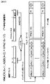
【図1】本発明の一実施例に係るマイクロコンピュータにおける複数ページサイズをサポートする構成の説明図である。
【図2】論理ページアドレスの一部をそのまま利用してTLBをインデックスする手法の説明図である。
【図3】論理ページアドレスの一部とプロセス番号の一部を用いてTLBをインデックスする手法の説明図である。
【図4】TLBエントリのリプレース対象バンクをソフトウェアで任意に決定可能とする構成の説明図である。
【図5】ページサイズの異なる論理アドレスとそれらをサポートするためのTLBエントリのフォーマットの一例を説明するための説明図である。
【図6】TLBのための各種レジスタの一例を説明するための説明図である。
【図7】本発明の一実施例に係るマイクロコンピュータの要部を示す全体ブロック図である。
【図8】本実施例のマイクロコンピュータがサポートするアドレスマップの一例を(A)及び(B)にて示す説明図である。
【図9】記憶保護に利用されるプロテクションビットPRによって規定されるアクセス権の説明図である。
【図10】アドレス変換の制御メインフローチャートである。
【図11】TLBのインデックス手法選択のための制御フローチャートである。
【図12】論理アドレスとそれによってインデックスされたタグとのアドレス比較の制御フローチャートである。
【図13】単一仮想記憶においてASIDをメモリ保護に利用する制御を含んだプロテクション制御の部分的なフローチャートである。
【図14】ページサイズに従った物理アドレス生成手順を示すフローチャートである。
【図15】リプレース対象バンクをハードウェア的に指定するための制御フローチャートである。
【図16】TLBミスにより生じる例外によって、起動されるところの TLBエントリを更新するためのTLBミスハンドラによる処理の一例を示すフローチャートである。
【図17】単一仮想記憶におけるTLBに関する例外検出処理の前半を示すフローチャートである。
【図18】単一仮想記憶におけるTLBに関する例外検出処理の後半を示すフローチャートである。
【図19】単一仮想記憶と多重仮想記憶との全体的な相違を示す説明図である。
【図20】単一仮想記憶と多重仮想記憶との概念を(A)及び(B)にて示す説明図である。
【図21】TLBの各バンクにおけるヒット信号に反映すべきアドレス比較結果を制御する制御ロジックの一例を示す論理回路図である。
【図22】図7の一部を更に詳細に示したブロック図である。
【符号の説明】
1 アドレス変換バッファ(バッファメモリ)
VPN 論理ページ番号
PPN 物理ページ番号
ASID,asid 空間番号(プロセス番号)
vpn 論理ページアドレス(論理ページ番号)
ppn 物理ページアドレス(物理ページ番号)
PR プロテクションキー
11〜14 バンク
15 比較手段
151〜153 コンパレータ
154 制御ロジック
2 インデックス用アドレス
XOR 排他的論理和ゲート
3 中央処理装置
4 キャッシュメモリ
5 TLBコントローラ
50 制御回路
51 PTEHレジスタ
52 PTELレジスタ
53 TTBレジスタ
54 TEAレジスタ
55 MMUCRレジスタ
SV シングルバーチャルビット
SZ サイズビット
IX インデックスモードビット
RC ランダムカウンタ
MD モードビット[0001]
[Industrial application fields]
The present invention relates to a data processing apparatus having an address conversion mechanism, and more particularly to a data processing apparatus using a set associative cache memory as an address conversion mechanism. For example, the present invention relates to a technique effective when applied to a microcomputer.
[0002]
[Prior art]
In a field where an operating system (hereinafter also referred to as OS) performs memory management without the user being aware of real memory, the data processing device needs to support an address translation mechanism. The address conversion mechanism is a mechanism for converting a logical address formed by a central processing unit (CPU) into a physical address in order to realize virtual storage. In order to execute this address translation mechanism at high speed, an address translation buffer (translation lookaside buffer, hereinafter simply referred to as TLB) holding a translation pair between a logical address and a physical address is built in the data processing apparatus together with the central processing unit. Technology is adopted. The address translation buffer is configured, for example, as a buffer memory having an associative memory structure that holds a translation pair of a recently used logical address and physical address. A buffer memory with an associative memory structure achieves a relatively high hit rate using a fully associative memory consisting of CAM (Content Addressable Memory) with a circuit configuration for comparison in each memory cell and a general-purpose random access memory. A set associative type associative memory can be used. As examples of documents describing the address conversion buffer in the associative memory format, there are “ultra-high-speed MOS devices” on pages 287 and 288 issued by Bafukan Co., Ltd. on February 10, 1986.
[0003]
[Problems to be solved by the invention]
The present inventor has examined the point that such an address translation buffer can meet the user's required specifications and realizes good usability, and has found the following problems.
[0004]
(1) In an address translation mechanism that supports virtual memory, a logical address space is divided into units called logical pages, and address translation to physical addresses is performed in units of pages. On the other hand, when the total storage capacity of the actual memory (physical memory) actually mounted in the system is small, the logical page size should be made relatively small to improve the memory utilization efficiency by each process. There is a request. For example, when a task to be executed is configured by a program having a relatively small size, if the size of a logical page allocated to the task is relatively large, the physical for executing the task is correspondingly corresponding to this. The page size is also relatively large. Therefore, more storage space than necessary is allocated to the task, and the memory utilization efficiency is reduced. In particular, when the storage capacity of the real memory is relatively small, it is desired to reduce the size of the logical page to prevent the use efficiency of the real memory from decreasing. In order to be able to respond appropriately to such a request, it is desirable to make the size of the logical page variable. However, when the size of the logical page is made variable, the number of bits of information for defining the logical page in a certain logical space is changed. As a result, the number of bits and the bit position of comparison target information for associatively retrieving information from the address translation buffer must be changed according to the logical page size. In order to cope with this, it is conceivable to adopt a full associative format composed of CAM for the address translation buffer. In this way, since each memory cell includes a comparison circuit, the logical page can be changed relatively easily without requiring special consideration. However, since each memory cell is provided with a comparison circuit, there is a drawback that both the chip-occupied area and the power consumption are doubled as compared with a set-associative address translation buffer.
[0005]
(2) In a set associative address translation buffer, if the number of banks in a plurality of sets, that is, the number of ways is increased, the number of entries that can be held for one index address can be increased, and the hit rate can be improved. . For example, in the case of the 4-way set associative format, a maximum of 4 entries can be held for one index address. However, when each of a plurality of processes has address translation information over the entire logical space and performs multiple virtual storage in which a logical address is modified or expanded by a process number, a relatively large number of processes are started in parallel. Each process uses the same logical page more frequently. Since the processes have different process numbers, the processes are held in different entries indicated by one index address. Therefore, when the number of processes exceeds the number of ways, the hit rate is relatively lowered even in the set associative format. Therefore, in a usage mode in which many processes are started in parallel in multiple virtual memories, it is necessary to be able to select an index method according to the usage mode so as to suppress a decrease in hit rate. Was found.
[0006]
(3) If the target translation pair is not stored in the address translation buffer, the translation pair related to the cache miss (desired translation pair) is added to the address translation buffer as a new entry. At this time, if all of the conversion pairs in the indexed entry are valid conversion pairs, the conversion pairs are replaced. This replacement algorithm (replacement algorithm) includes random, FIFO that replaces the first loaded one, or LRU (Least Recentry Used) that replaces the one last referenced. However, when the replacement algorithm is fixed, for the sake of data processing, a request to always store a specific conversion pair as an entry in the address conversion buffer or a specific address conversion pair is not desired to be replaced. I can't answer any request.
[0007]
(4) In addition to the above-described multiple virtual memory, there is a single virtual memory in which a part of the logical address space is exclusively allocated to a plurality of processes. It is desirable to be able to support both of these in terms of improving usability.
[0008]
An object of the present invention is to realize a data processing apparatus having an address translation mechanism that can meet user's required specifications and is easy to use.
[0009]
The object of the present invention will be described in further detail as follows. To provide a data processing apparatus having an address conversion mechanism capable of supporting a plurality of page sizes without increasing a chip exclusive area and power consumption.
[0010]
A data processing apparatus including an address translation mechanism that supports a plurality of index methods and from which an index method can be selected.
[0011]
To provide a data processing device including an address conversion mechanism that can give a degree of freedom to a replacement target of an address conversion pair.
[0012]
In addition, the present invention provides a data processing apparatus having an address translation mechanism that can give a degree of freedom to a virtual storage format that can be supported.
[0013]
The above and other objects and novel features of the present invention will be apparent from the description of this specification and the accompanying drawings.
[0014]
[Means for Solving the Problems]
The following is a brief description of an outline of typical inventions disclosed in the present application.
[0015]
<< Supporting Multiple Page Sizes >> A data processing apparatus that supports virtual storage divides a logical address space into units called logical pages, and converts logical addresses into physical addresses (address conversion) in units of pages. In this data processing apparatus, as illustrated in FIG. 1, the size of the logical page is variable for each page. A
[0016]
The maximum size of the logical page to be supported is a power of 2 times the minimum size (2 to the power of N), and the number of banks of the set associative buffer memory is greater than the power of 2 (the power of 2 to the N power). Is done. More specifically, as illustrated in FIG. 1, in a logical address space (specified by a logical address of
[0017]
In the above address translation buffer, the index address designation method for the
[0018]
In order to determine the TLB hit / miss, the number of bits for address comparison to be reflected in the hit determination in the comparison means 15 provided in each
[0019]
<< Supporting multiple index methods >> Data processing devices that support virtual storage each have storage areas for storing correspondence information between logical page numbers and physical page numbers, and each is accessed by a common index address. A buffer memory composed of a set associative cache memory having a plurality of banks. And it has a means to make variable the index address generation method for the buffer memory. For example, in the case where there are a plurality of processes, each process has respective address translation information, and supports multiple virtual memories in which each process is distinguished by a process number, an address for indexing an entry from the buffer memory As a designation method, a method of decoding only a part of the logical address (
[0020]
<< Degree of Freedom of Replacement >> As illustrated in FIG. 4, each data processing device that supports virtual storage provides storage areas for storing correspondence information between logical page numbers VPN and physical page numbers PPN, respectively. Have a
[0021]
As illustrated in FIG. 4, the hardware means includes MMUCR. RC is provided as a counting means such as a random counter, and the power of 2 of the number of bits of the counting means matches the number of banks (= 4) of the
[0022]
<< Support for Single Virtual Storage and Multiple Virtual Storage >> A data processing device that supports virtual storage divides the logical address space into units called logical pages, and converts the logical addresses into physical addresses for each page. It has an address translation mechanism to do it. This address translation mechanism includes a multiple virtual memory that modifies or expands a logical address by a process number (asid) when each of a plurality of processes has address translation information over the entire logical space, and a logical address space of a plurality of processes Having a single virtual memory that does not qualify or extend a logical address by a process number (asid) when a portion is allocated exclusively and each process has address translation information for the logical address space assigned to it, The multiple virtual memory and the single virtual memory can be selected. Therefore, as illustrated in FIG. 5, each entry in the buffer memory is provided with a process number ASID field in addition to a conversion pair of a logical page number VPN and a physical page number PPN. The contents of this field differ depending on whether it is a single virtual memory or a multiple virtual memory. When a logical page corresponding to a process number included in a certain TLB entry cannot be shared with other processes, the contents of the field of the process number ASID are the hit / Used to determine a miss (TLB hit / TLB miss). That is, in this case, the information on the logical page number VPN of the entry stored in the buffer memory matches the information on the logical page address vpn, and the process number ASID of the entry matches the current process number asid. Otherwise, it will not be a TLB hit. In the single virtual memory, the contents of the field of the process number ASID are used as memory protection information. That is, in this case, when a TLB miss occurs due to a process number difference, the software determines whether the TLB miss is caused by a process number difference or a logical page address difference. In the case of, it is processed as a protection error. Whether the single virtual memory or the multiple virtual memory is the bit MMUCR. Of the register MMUCR illustrated in FIG. Indicated by the value of SV. This bit MMUCR. The value of SV can be arbitrarily set by software executed by the central processing unit.
[0023]
[Action]
A data processing apparatus that selectively supports multiple page sizes can reduce the size of logical pages when the total storage capacity of real memory installed in the system is small, and the memory usage efficiency by each process It is possible to easily meet the demand to improve the quality. At this time, the maximum logical page size is set to a power of 2 times the minimum size, and the number of banks of the set associative buffer memory is set to a power of 2 or more. Regardless of the size of the selected logical page, in principle, the same number of entries can be held in the buffer memory for any logical page number entry. Changing the number of bits of the address comparison to be reflected in the hit determination using information for indicating the size of the logical page means changing the number of bits and the bit position of the comparison target information for associatively searching the buffer memory. It can be easily changed according to the size of the logical page. Realizing a buffer memory that supports a plurality of page sizes with a set-associative cache memory halves both the chip-occupied area and the power consumption compared to the case where it is configured with a CAM.
[0024]
According to the means for supporting a plurality of indexing methods, the indexing method can be set according to the usage mode so that a decrease in hit rate can be suppressed in a usage mode in which many processes are started in parallel in multiple virtual memory. Can be selectable. A hit in a usage mode in which many processes are started in parallel in multiple virtual memory by qualifying a part of the logical address with a process number (asid) using the logical address and indexing the buffer memory with this. It is possible to suppress a decrease in rate.
[0025]
According to the means for improving the degree of freedom of replacement, it is possible to arbitrarily determine the bank to be replaced by software without fixing the replacement algorithm for replacing the conversion pair of the buffer memory. As a result, it is possible to easily respond to a request to always store a specific translation pair as an entry in the address translation buffer for convenience of data processing or a request not to make a specific address translation pair to be replaced. . Having a register for designating a replacement target by software can guarantee the degree of freedom of replacement according to random, FIFO, LRU, or the like, depending on the algorithm of the software.
[0026]
According to the means for supporting single virtual memory and multiple virtual memory, the usability of the address translation mechanism can be improved. In particular, it is possible to select which one to use via software, thereby further improving usability. By using the process number (ASID) in the multiple virtual memory as the memory protection information in the single virtual memory, it is possible to easily realize complete memory protection when the single virtual memory is selected.
[0027]
【Example】
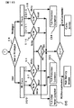
<< Microcomputer >> FIG. 7 shows a main part of a microcomputer as an embodiment of the data processing apparatus according to the present invention. The microcomputer of the present embodiment is not particularly limited, but is formed on a single semiconductor substrate such as single crystal silicon by a known semiconductor integrated circuit manufacturing technique. The figure shows a logical address bus VABUS, a physical address bus PABUS, a data bus DBUS, a central processing unit (CPU) 3, a cache memory (CACHE) 4, an address translation buffer (TLB) 1 as a buffer memory, and a TLB controller ( TLBC) 5 is shown as a representative circuit block. The
[0028]
The microcomputer according to this embodiment divides a logical address space into units called logical pages, and supports virtual storage for performing address conversion from logical addresses to physical addresses in units of pages. The
[0029]
Here, the address space of the microcomputer of this embodiment will be described in advance. Since the microcomputer of this embodiment supports a 4 GB logical address space, the
[0030]
As described above, the microcomputer according to the present embodiment has the privileged mode and the user mode, and the status included in the
[0031]
The 4 GB logical address space shown in FIGS. 8A and 8B is not particularly limited, but the P0 area and the P3 area are divided into a plurality of units called logical pages and divided page units. Thus, the logical address is converted into a physical address. There are two types of logical page sizes supported by the microcomputer of this embodiment: 4 KB and 1 KB. This is because the maximum logical page size (= 4 KB) supported is a power of 2 times the minimum size (= 1 KB), and the number of banks of the address translation buffer 1 (= 4) is greater than the power of 2 Satisfy the relationship of As shown in FIG. 5, when the logical page size is 1 KB,
[0032]
When a TLB miss or the like occurs, information (page table entry) taken into the entry in the
[0033]
The entries stored in each bank in the
[0034]
Here, the concept of single virtual memory and multiple virtual memory will be described with reference to FIGS. The multiple virtual memory means that when each of a plurality of processes has address conversion information over the entire logical space, the logical address is modified or expanded by the process number asid. On the other hand, in the single virtual memory, a part of the logical address space is exclusively allocated to a plurality of processes. In other words, in the single virtual memory, when each process has the address translation information of the logical address space assigned to it, the logical address is not modified or expanded by the process number asid. Thus, in a single virtual memory, a logical address space is exclusively allocated among a plurality of processes. Therefore, as shown in FIG. 20B, for each logical address space allocated to a process. There is unique address translation information. Therefore, there is only one address conversion table. If the one address conversion table is used, a certain logical address A is uniquely converted into a physical address D corresponding thereto. On the other hand, in the multiple virtual memory, logical address spaces are allocated overlappingly among a plurality of processes. For this reason, the address translation information for each process must be included in different address translation tables. Therefore, a certain logical address A is converted into different physical addresses B and C through different address conversion tables i and j. At this time, the process number identifies the process to which the logical address A related to the conversion belongs. According to FIG. 20A, in the multiple virtual memory, the address conversion table i corresponds to the process number i, and the address conversion table j corresponds to the process number j. The process number can be regarded as an identification number in a plurality of processes that use (access) the same logical address space.
[0035]
FIG. 19 shows the difference between single virtual storage and multiple virtual storage regarding logical space, conversion information, and protection. In this drawing, PR is the protection information shown in FIG.
[0036]
In FIG. 7, the
[0037]
As shown in FIG. 6, the
[0038]
In FIG. 7, of the logical page number vpn (31-10) of the logical address output from the
[0039]
FIG. 21 shows an example of a logical configuration of the
[0040]
The OR gate 1543 includes the output of the
[0041]
In the single virtual memory, the process number ASID held by the TLB entry is used as memory protection information (domain number). Sharing or non-sharing is instructed by the shared bit SH in both single virtual memory and multiple virtual memory. When non-sharing is instructed, in the multiple virtual memory, a mismatch between the current process number asid and the process number ASID included in the TLB entry is regarded as a TLB miss. On the other hand, when non-sharing is instructed, in the single virtual memory, the mismatch between the process numbers asid and ASID is used for detecting a TLB protection violation exception. In order to realize this, the
[0042]
FIG. 10 is a main flowchart showing control of the address conversion operation by the
[0043]
In the index processing L1 of the
[0044]
An example of the address comparison procedure executed in the address comparison and V-bit check processing L2 is shown in FIG. The procedure shown here is based on the logic of the
[0045]
Based on the index, a TLB entry is read from TLB1, and based on the shared status SH in the read TLB entry, it is determined whether or not to consider the space number ASID in the address comparison. When SH = 1 (shared), the space number ASID is not considered as an address comparison target, and when SH = 0 (non-shared), the space number ASID is considered as an address comparison target. Further, the SV value (MMUCR.SV) of the
[0046]
In this embodiment, the size of 1 KB or 4 KB is selected as the size of the logical page according to the value of the size bit SZ in the TLB entry. When the size of the logical page is 1 KB, the information VPN (31-17) and VPN (11-10) in each TLB entry indexed in each bank are the corresponding bits vpn (31-17) of the logical address. , Vpn (11-10). When the logical page size is 4 KB, the VPN (11-10) and the corresponding logical address vpn (11-10) among the information VPNs in each TLB entry indexed in each bank are as follows. It is excluded from the target of comparison judgment.
[0047]
As described above, comparison targets (VPN (31-17, 11-10), vpn (31-17, 11-10), ASID, asid) are determined, and comparison is performed. As a result of this comparison, if any bank matches, a hit signal is output from the matched bank. The hits in each bank are output as hit signals hit1 to hit4 and are TLB hits. On the other hand, if no hit signal is output from any bank, that is, if there is a mismatch, a TLB miss exception will be detected. The result is also notified to the
[0048]
Also, for each banked entry in the index, a check is made for the V bit in that entry. In other words, the V bit in the read entry is checked by the index. In the case of a TLB hit, when the V bit in the entry related to the hit is 0 (invalid), a TLB invalid exception is detected and notified to the
[0049]
In the access right check processing L3, the contents of the information PR in the TLB entry read by the index and the bits MMUCR. The access right is checked according to the contents of the SV. For example, as shown in FIG. 13, first, the bits MMUCR. It is determined whether the SV is 1 (single virtual memory) or 0 (multiple virtual memory). In the case of multiple virtual storage (SV = 0), protection of the address space represented by the information in the TLB entry is performed according to the contents of the PR shown in FIG. When in single virtual memory and in privileged mode, ie MMUCR. When SV = 1 (single virtual memory), bits SR. When MD = 1 (privileged mode), the address space represented by the information in the TLB entry can be accessed unconditionally. On the other hand, even in the case of a single virtual memory, in the case of the user mode (SR.MD = 0: user mode), the space number ASID and the shared status SH are considered when checking the access right. That is, when the space number asid of the
[0050]
In the physical address generation process L4, a physical address is generated as shown in FIG. 14 in accordance with the size bit SZ of the indexed TLB entry. The offset va (9-0) of the logical address va used to form the physical address pa is not shown in the figure, but is held in a latch circuit in the control circuit (CTRL) 50. When SZ = 0 (logical page size is 1 KB), the offset va (9-0) of the logical address va output from the
[0051]
FIG. 15 shows a hardware designation method of the replacement target bank in the TLB miss exception detected in the address comparison and V-bit check processing L2. This control is uniquely performed by the
[0052]
FIG. 16 shows a processing procedure by the TLB miss handler for updating the TLB entry in order to deal with the TLB miss exception. The load TLB instruction is used to update the TLB1 entry. The load TLB instruction (also referred to as LDTLB) is executed by the
[0053]
In order to cope with the TLB miss exception, a page table is formed in advance in the external memory RAM as shown in FIG. In the page table, although not particularly limited, a plurality of pieces of conversion information (page table entries) respectively corresponding to a plurality of logical addresses are stored according to a predetermined rule. The page table address, for example, its start address is stored in advance in the
[0054]
The TLB miss handler is described by the user. When a TLB miss exception is detected, this TLB miss handler is activated by the
[0055]
The TLB invalid exception occurs in the case of a page fault in a TLB hit. For this exception, for example, first, the page table entry in the external memory is recovered, and the V bit in the page table entry is set to the
[0056]
When the TLB initial page write exception is detected, the D bit of the corresponding page table entry on the external memory is set to the
[0057]
When the TLB protection violation exception is detected, in order to resolve the protection violation after the logical page number vpn of the logical address as the exception cause is written in the
[0058]
As mentioned above, MMUCR. When RC is used as a counter, it is desirable to increment as described above in order to be able to register an entry in a new bank when taking measures against the TLB miss exception. On the other hand, in the countermeasure against the TLB invalid exception, the TLB initial page write exception, and the TLB protection violation exception, the MMUCR. It is desirable not to increment RC. In these measures, there is a case where only the D bit or V bit needs to be changed, so that it is possible to use the TLB more effectively by registering in the original bank without registering in the new bank. . Of course, the present invention is not limited to this.
[0059]
17 and 18 show the bits MMUCR. The entire exception detection flow related to TLB1 when SV is set to 0 and multiple virtual storage is instructed is shown. According to FIG. 17, the index of TLB1 is performed by a predetermined method according to the logical address vpn and the current space number asid (S1). When the indexed entry includes SH = 0 (non-shared), if the ASID or VPN does not match (S3), a TLB miss exception (EX1) is detected. If the indexed entry contains SH = 1 (shared), the ASID is not compared and if the VPNs do not match (S4), a TLB miss exception (EX1) is detected. In the case of a TLB hit (YES in S3 and S4), it is determined whether or not V = 1 (S5). If V = 0 (invalid), a TLB invalid exception (EX2) is detected. When V = 1 (valid), as shown in FIG. It is determined from the MD whether the user mode (User) or the privileged mode (Privileged) (S6). Information indicating that the
[0060]
If PR = 00 or 10 is also determined in the access in the privileged mode, a TLB protection violation exception (EX4) is detected if the read / write access type is contrary to the PR contents (write in S8). Is done. That is, the access right permitted by the PR differs depending on whether the
[0061]
FIG. 22 mainly shows the connection relationship between the registers shown in FIG. 7 and the central processing unit CPU. Each register is assigned a unique address. The logical address formed by the central processing unit CPU3 is supplied to the selection circuit in the control circuit (TLBC) 50 via the internal logical address bus VABUS. The selection circuit decodes the logical address, and when the logical address is a unique address assigned to the register, generates a selection signal for selecting the register. For example, when the logical address is an address assigned to the
[0062]
The internal logical address bus VABUS is also connected to the control circuit (CTRL) 50 and TLB1. The control circuit (CTRL) 50 is provided with a latch circuit for holding the offset of the logical address as described above, and holds the offset of the logical address from the internal logical address bus VABUS. Further, a logical address is supplied from the
[0063]
In the drawing, only the connection between the
[0064]
The internal data bus DBUS and the internal physical address bus PABUS are connected to the external data bus DBUS and the external address bus ABUS via external terminals TD and TA provided in the data processing device. For example, as shown in the figure, external memory RAM and ROM are connected to these external buses. Although not particularly limited, the external memory RAM is a volatile memory, and various tables as described above are formed. The external memory ROM is a nonvolatile memory, and stores various programs (for example, software such as the above-described handler).
[0065]
In the following, the effect of the virtual memory in the microcomputer of this embodiment will be described for each feature point.
[0066]
<< Support of Multiple Page Sizes >> As shown in FIGS. 5 and 6, the page table entry and the TLB entry have the size bit SZ, and the size of the logical page can be set for each page. The 4-way set associative
[0067]
The number of bits of address comparison for hit determination must be changed according to the logical page size as described with reference to FIG. When the logical page size is 1 KB, vpn (11-10) must be compared with VPN (11-10) compared to the case of 4 KB. The
[0068]
In this way, a macro computer that selectively supports multiple page sizes can reduce the size of logical pages and reduce the memory usage efficiency of each process when the total storage capacity of the real memory installed in the system is small. It is possible to easily meet the demand to improve the quality. At this time, the maximum logical page size is set to a power of 2 times the minimum size, and the number of banks of the TLB1 of the set associative method is set to a power of 2 or more, whereby the index address designation method is set to the maximum logical page. Regardless of whether the size is unified or the selected logical page size is the maximum or minimum, in principle, any logical page number entry can be held in the
[0069]
<< Supporting multiple indexing methods >> When there are multiple processes, each process has its own address translation information, and supports multiple virtual storage where each process is distinguished by the process number asid, As a method of designating the index address of TLB1, a method of decoding only a part of the logical address (index address) as shown in FIG. 2 and its logical address by exclusive OR gate XOR as shown in FIG. And a method of decoding a result obtained by modifying a part (index address) of the current process number asid with a bit MMUCR. It can be indicated according to the logical value of IX. According to this, it is possible to select an index method according to the usage mode so that a decrease in hit rate can be suppressed in a usage mode in which many processes are started in parallel in multiple virtual memory. . In addition, a part of the logical address is modified by the number asid of the process that uses the logical address, and the buffer memory is indexed by this. Reduction in rate can be suppressed.
[0070]
<< Freedom of Replacement >> As described above, the
[0071]
In this way, the replacement algorithm for replacing the entry of
[0072]
<< Support of Single Virtual Memory and Multiple Virtual Memory >> In the microcomputer of this embodiment, when each of a plurality of processes to be executed has address conversion information over the entire logical space, the logic is indicated by the process number asid. Multiple virtual memories that qualify or extend addresses, and a part of the logical address space is exclusively allocated to a plurality of processes to be executed, and address conversion information of the logical address space to which each process is allocated If so, it is possible to select a single virtual memory that does not qualify or extend the logical address by the process number asid. Such control for virtual memory is controlled by the MMUCR.exe illustrated in FIG. Indicated by the value of SV. MMUCR. The value of SV is arbitrarily set by the
[0073]
MMUCR. By setting the SV value via the
[0074]
Although the invention made by the present inventor has been specifically described based on the embodiments, it is needless to say that the present invention is not limited thereto and can be variously modified without departing from the gist thereof.
[0075]
For example, in the above embodiment, the number of TLB ways, that is, the number of banks can be set to 5 or more, for example, 8. For example, when the page size is 1 KB and 8 KB, the number of LTB ways (the number of banks) may be 8 or more. When the page size is 4 KB and 16 KB, the number of LTB ways (the number of banks) may be four or more. The effect similar to the said Example can be acquired also by them. In short, the maximum size of the supported page is set to a power of 2 times the minimum size, and the number of sets of the buffer memory of the set associative method may be equal to or greater than the power of 2. The size of the address space supported by the microcomputer is not limited to 4 GB, and the number of bits of the logical address is not limited accordingly. The supported page size can be changed to an appropriate size, and the number of supported types can be changed as appropriate. Further, the logical page number VPN held as the TLB entry is not limited to the configuration excluding the corresponding bits used for the index as in the above embodiment, and all bits of the logical page number are held as the TLB entry. You can also.
[0076]
In the above description, the case where the invention made mainly by the present inventor is used in the microcomputer which is the field of use behind the present invention has been described. However, the present invention is not limited to this, for example, for an MMU (memory management unit). It can be widely applied to controller chips and the like.
[0077]
【The invention's effect】
The effects obtained by the representative ones of the inventions disclosed in the present application will be briefly described as follows.
[0078]
That is, it is possible to realize a data processing apparatus that can support a plurality of page sizes without increasing the chip occupation area and the power consumption. An address translation mechanism capable of selecting an index method can be realized. A degree of freedom can be given to the replacement target of the address translation pair. In addition, it is possible to give a degree of freedom to virtual storage formats that can be supported. As a result, it is possible to realize a data processing apparatus that can meet the user's required specifications and has an easy-to-use address translation mechanism.
[Brief description of the drawings]
FIG. 1 is an explanatory diagram of a configuration that supports a plurality of page sizes in a microcomputer according to an embodiment of the present invention;
FIG. 2 is an explanatory diagram of a technique for indexing a TLB by using a part of a logical page address as it is.
FIG. 3 is an explanatory diagram of a technique for indexing a TLB using a part of a logical page address and a part of a process number.
FIG. 4 is an explanatory diagram of a configuration in which a replacement target bank of a TLB entry can be arbitrarily determined by software.
FIG. 5 is an explanatory diagram for explaining an example of logical addresses having different page sizes and a format of a TLB entry for supporting them.
FIG. 6 is an explanatory diagram for explaining an example of various registers for TLB;
FIG. 7 is an overall block diagram showing a main part of a microcomputer according to an embodiment of the present invention.
FIGS. 8A and 8B are explanatory diagrams illustrating an example of an address map supported by the microcomputer according to the present embodiment, in FIGS.
FIG. 9 is an explanatory diagram of an access right defined by a protection bit PR used for storage protection.
FIG. 10 is a control main flowchart of address translation.
FIG. 11 is a control flowchart for selecting a TLB index method;
FIG. 12 is a control flowchart of address comparison between a logical address and a tag indexed by the logical address.
FIG. 13 is a partial flowchart of protection control including control for using an ASID for memory protection in a single virtual memory.
FIG. 14 is a flowchart showing a physical address generation procedure according to the page size.
FIG. 15 is a control flowchart for designating a replacement target bank in hardware.
FIG. 16 is a flowchart showing an example of processing by a TLB miss handler for updating a TLB entry that is activated by an exception caused by a TLB miss.
FIG. 17 is a flowchart showing the first half of exception detection processing related to TLB in a single virtual memory;
FIG. 18 is a flowchart showing the second half of the exception detection process related to TLB in a single virtual memory.
FIG. 19 is an explanatory diagram showing an overall difference between single virtual storage and multiple virtual storage.
FIG. 20 is an explanatory diagram showing the concept of single virtual storage and multiple virtual storage in (A) and (B).
FIG. 21 is a logic circuit diagram showing an example of control logic for controlling an address comparison result to be reflected in a hit signal in each bank of a TLB.
FIG. 22 is a block diagram showing a part of FIG. 7 in more detail.
[Explanation of symbols]
1 Address translation buffer (buffer memory)
VPN logical page number
PPPN physical page number
ASID, asid space number (process number)
vpn logical page address (logical page number)
ppn physical page address (physical page number)
PR protection key
11-14 banks
15 Comparison means
151-153 Comparator
154 Control logic
2 Index address
XOR exclusive OR gate
3 Central processing unit
4 cache memory
5 TLB controller
50 Control circuit
51 PTEH register
52 PTEL register
53 TTB register
54 TEA register
55 MMUCR register
SV single virtual bit
SZ size bit
IX Index mode bit
RC random counter
MD mode bit
Claims (3)
上記バッファメモリは、複数のバンクを有し、上記複数のバンクは、それぞれが複数のメモリフィールドを有し、上記複数のメモリフィールドはそれぞれの仮想ページ毎の仮想ページ情報、仮想ページ情報に対応した物理ページ情報、仮想ページのサイズ情報を格納可能であり、
上記物理アドレスに変換されるべき論理アドレスは、第1の論理アドレスデータおよび第2の論理アドレスデータを含み、
上記選択回路は、上記第1の論理アドレスデータに応じて、上記複数のバンクのそれぞれからメモリフィールドを選択し、
上記第1の論理アドレスデータは論理アドレスのビット配列中の第1のビット領域の情報であり、
上記比較回路は、選択されたメモリフィールドに含まれる仮想ページ情報と上記第2の論理アドレスデータとを比較し、
上記第2の論理アドレスデータは論理アドレスのビット配列中の第2のビット領域の情報であり、
上記第2のビット領域のビット数は、選択されたメモリフィールドに含まれるサイズ情報に応じて決定され、
上記仮想ページの最大サイズは最小サイズの2のN乗倍にされ、
上記バッファメモリのバンクの数は上記2のN乗個以上であり、
上記バッファメモリは、上記仮想ページのサイズ情報に拘わらずに、設定可能な複数の仮想ページのサイズのうち最大ページサイズの上記第1の論理アドレスデータがインデックスアドレスとして上記選択回路に供給されるものであり、
最大ページサイズの上記第1の論理アドレスデータは当該最大ページサイズの仮想ページ情報における最下位から上位側への連続複数ビットであることを特徴とするデータ処理装置。The logical address space is divided into a plurality of virtual pages, has a virtual storage function in which logical addresses are converted into physical addresses in units of virtual pages, and has a buffer memory, a selection circuit, and a comparison circuit,
The buffer memory has a plurality of banks, each of the plurality of banks has a plurality of memory fields, and the plurality of memory fields correspond to virtual page information and virtual page information for each virtual page. Physical page information and virtual page size information can be stored,
Logical address to be translated into the physical address comprises a first logical address data and the second logical address data,
It said selection circuit, in accordance with the first logical address data, select the memory field from each of the plurality of banks,
The first logical address data is information of a first bit area in a bit array of logical addresses ,
The comparison circuit compares the virtual page information and the second logical address data contained in the memory field selected,
The second logical address data is information of a second bit area in the bit array of the logical address ,
The number of bits of the second bit area is determined according to size information included in the selected memory field,
The maximum size of the upper Kikari virtual page is the second N th power of minimum size,
The number of banks of the buffer memory is the N-th power number than the above two,
In the buffer memory, the first logical address data having the maximum page size among a plurality of settable virtual page sizes is supplied to the selection circuit as an index address regardless of the size information of the virtual page. And
The data processing apparatus according to claim 1, wherein the first logical address data having the maximum page size is a plurality of consecutive bits from the lowest order to the higher order in the virtual page information having the maximum page size .
上記第2ビットの比較がヒット判定に反映されるかどうかは、上記サイズ情報により決定されることを特徴とする請求項1のデータ処理装置。 The virtual page information included in the memory field, a field for storing first bits for virtual page size is compared with the second logical address data in the case of maximum size, when the virtual page size is the maximum size A field for storing a second bit that is not compared with the second logical address data and is compared with the logical address data when the virtual page size is the minimum size;
Above whether comparison of the second bit is reflected in the hit determination, the data processing apparatus according to claim 1, characterized in that it is determined by the size information.
Priority Applications (8)
| Application Number | Priority Date | Filing Date | Title |
|---|---|---|---|
| JP24087195A JP3740195B2 (en) | 1994-09-09 | 1995-08-25 | Data processing device |
| EP95113771A EP0701211B1 (en) | 1994-09-09 | 1995-09-01 | Data processor with address translation mechanism |
| EP99120560A EP0977123A3 (en) | 1994-09-09 | 1995-09-01 | Data processor with address translation mechanism |
| DE69520718T DE69520718T2 (en) | 1994-09-09 | 1995-09-01 | Data processor with address translation mechanism |
| KR1019950029114A KR100368196B1 (en) | 1994-09-09 | 1995-09-06 | Data processing device |
| US08/524,561 US5796978A (en) | 1994-09-09 | 1995-09-07 | Data processor having an address translation buffer operable with variable page sizes |
| US08/657,231 US5907867A (en) | 1994-09-09 | 1996-06-03 | Translation lookaside buffer supporting multiple page sizes |
| US09/007,249 US6047354A (en) | 1994-09-09 | 1998-01-14 | Data processor for implementing virtual pages using a cache and register |
Applications Claiming Priority (5)
| Application Number | Priority Date | Filing Date | Title |
|---|---|---|---|
| JP6-241993 | 1994-09-09 | ||
| JP24199394 | 1994-09-09 | ||
| JP7-86068 | 1995-03-17 | ||
| JP8606895 | 1995-03-17 | ||
| JP24087195A JP3740195B2 (en) | 1994-09-09 | 1995-08-25 | Data processing device |
Related Child Applications (1)
| Application Number | Title | Priority Date | Filing Date |
|---|---|---|---|
| JP2005000091A Division JP2005108262A (en) | 1994-09-09 | 2005-01-04 | Data processor |
Publications (2)
| Publication Number | Publication Date |
|---|---|
| JPH08320830A JPH08320830A (en) | 1996-12-03 |
| JP3740195B2 true JP3740195B2 (en) | 2006-02-01 |
Family
ID=27305071
Family Applications (1)
| Application Number | Title | Priority Date | Filing Date |
|---|---|---|---|
| JP24087195A Expired - Fee Related JP3740195B2 (en) | 1994-09-09 | 1995-08-25 | Data processing device |
Country Status (5)
| Country | Link |
|---|---|
| US (2) | US5796978A (en) |
| EP (2) | EP0977123A3 (en) |
| JP (1) | JP3740195B2 (en) |
| KR (1) | KR100368196B1 (en) |
| DE (1) | DE69520718T2 (en) |
Families Citing this family (121)
| Publication number | Priority date | Publication date | Assignee | Title |
|---|---|---|---|---|
| US5918251A (en) * | 1996-12-23 | 1999-06-29 | Intel Corporation | Method and apparatus for preloading different default address translation attributes |
| US5950228A (en) * | 1997-02-03 | 1999-09-07 | Digital Equipment Corporation | Variable-grained memory sharing for clusters of symmetric multi-processors using private and shared state tables |
| KR100263672B1 (en) * | 1997-05-08 | 2000-09-01 | 김영환 | Apparatus for address transition supporting of varable page size |
| JPH10333971A (en) * | 1997-05-28 | 1998-12-18 | Sony Corp | Data arithmetic unit |
| DE19735948C1 (en) * | 1997-08-19 | 1998-10-01 | Siemens Nixdorf Inf Syst | Method for improving controllability in data processing equipment with translation-look-aside-buffer (TLB) |
| US6851036B1 (en) * | 1997-11-06 | 2005-02-01 | Renesas Technology Corp. | Method and apparatus for controlling external devices through address translation buffer |
| DE69815482T2 (en) * | 1997-12-24 | 2004-04-29 | Texas Instruments Inc., Dallas | Computer arrangement with processor and memory hierarchy and its operating method |
| US6289431B1 (en) * | 1998-01-26 | 2001-09-11 | Intel Corporation | Method and apparatus for accessing more than 4 Gigabytes of physical memory with 4-byte table entries |
| US6266754B1 (en) * | 1998-05-29 | 2001-07-24 | Texas Instruments Incorporated | Secure computing device including operating system stored in non-relocatable page of memory |
| US6603768B1 (en) | 1998-06-27 | 2003-08-05 | Intel Corporation | Multi-protocol conversion assistance method and system for a network accelerator |
| US6311212B1 (en) * | 1998-06-27 | 2001-10-30 | Intel Corporation | Systems and methods for on-chip storage of virtual connection descriptors |
| US6657959B1 (en) | 1998-06-27 | 2003-12-02 | Intel Corporation | Systems and methods for implementing ABR with guaranteed MCR |
| US6728249B2 (en) | 1998-06-27 | 2004-04-27 | Intel Corporation | System and method for performing cut-through forwarding in an ATM network supporting LAN emulation |
| US6724767B1 (en) | 1998-06-27 | 2004-04-20 | Intel Corporation | Two-dimensional queuing/de-queuing methods and systems for implementing the same |
| US6735773B1 (en) | 1998-06-27 | 2004-05-11 | Intel Corporation | Method and apparatus for issuing commands to a network processor configured to provide a plurality of APIs |
| US6604136B1 (en) | 1998-06-27 | 2003-08-05 | Intel Corporation | Application programming interfaces and methods enabling a host to interface with a network processor |
| US6226731B1 (en) * | 1998-09-08 | 2001-05-01 | International Business Machines Corporation | Method and system for accessing a cache memory within a data-processing system utilizing a pre-calculated comparison array |
| DE19842849C2 (en) * | 1998-09-18 | 2001-02-01 | Siemens Ag | Method and arrangement for transmitting digital data |
| US6910109B2 (en) * | 1998-09-30 | 2005-06-21 | Intel Corporation | Tracking memory page state |
| US6542983B1 (en) | 1999-10-01 | 2003-04-01 | Hitachi, Ltd. | Microcomputer/floating point processor interface and method |
| US6701405B1 (en) | 1999-10-01 | 2004-03-02 | Hitachi, Ltd. | DMA handshake protocol |
| US6772325B1 (en) * | 1999-10-01 | 2004-08-03 | Hitachi, Ltd. | Processor architecture and operation for exploiting improved branch control instruction |
| US6590907B1 (en) | 1999-10-01 | 2003-07-08 | Stmicroelectronics Ltd. | Integrated circuit with additional ports |
| US6487683B1 (en) | 1999-10-01 | 2002-11-26 | Stmicroelectronics Limited | Microcomputer debug architecture and method |
| US6598128B1 (en) | 1999-10-01 | 2003-07-22 | Hitachi, Ltd. | Microprocessor having improved memory management unit and cache memory |
| US6463553B1 (en) | 1999-10-01 | 2002-10-08 | Stmicroelectronics, Ltd. | Microcomputer debug architecture and method |
| US6598177B1 (en) | 1999-10-01 | 2003-07-22 | Stmicroelectronics Ltd. | Monitoring error conditions in an integrated circuit |
| US7793261B1 (en) | 1999-10-01 | 2010-09-07 | Stmicroelectronics Limited | Interface for transferring debug information |
| US6412047B2 (en) | 1999-10-01 | 2002-06-25 | Stmicroelectronics, Inc. | Coherency protocol |
| US6434665B1 (en) | 1999-10-01 | 2002-08-13 | Stmicroelectronics, Inc. | Cache memory store buffer |
| US6557119B1 (en) | 1999-10-01 | 2003-04-29 | Stmicroelectronics Limited | Microcomputer debug architecture and method |
| US6826191B1 (en) | 1999-10-01 | 2004-11-30 | Stmicroelectronics Ltd. | Packets containing transaction attributes |
| US7260745B1 (en) | 1999-10-01 | 2007-08-21 | Stmicroelectronics Ltd. | Detection of information on an interconnect |
| US7000078B1 (en) | 1999-10-01 | 2006-02-14 | Stmicroelectronics Ltd. | System and method for maintaining cache coherency in a shared memory system |
| US6460174B1 (en) | 1999-10-01 | 2002-10-01 | Stmicroelectronics, Ltd. | Methods and models for use in designing an integrated circuit |
| US6591369B1 (en) | 1999-10-01 | 2003-07-08 | Stmicroelectronics, Ltd. | System and method for communicating with an integrated circuit |
| US6349371B1 (en) | 1999-10-01 | 2002-02-19 | Stmicroelectronics Ltd. | Circuit for storing information |
| US7072817B1 (en) | 1999-10-01 | 2006-07-04 | Stmicroelectronics Ltd. | Method of designing an initiator in an integrated circuit |
| US6546480B1 (en) | 1999-10-01 | 2003-04-08 | Hitachi, Ltd. | Instructions for arithmetic operations on vectored data |
| US6298394B1 (en) | 1999-10-01 | 2001-10-02 | Stmicroelectronics, Ltd. | System and method for capturing information on an interconnect in an integrated circuit |
| US6457118B1 (en) | 1999-10-01 | 2002-09-24 | Hitachi Ltd | Method and system for selecting and using source operands in computer system instructions |
| US6629207B1 (en) | 1999-10-01 | 2003-09-30 | Hitachi, Ltd. | Method for loading instructions or data into a locked way of a cache memory |
| US6665816B1 (en) | 1999-10-01 | 2003-12-16 | Stmicroelectronics Limited | Data shift register |
| US6502210B1 (en) | 1999-10-01 | 2002-12-31 | Stmicroelectronics, Ltd. | Microcomputer debug architecture and method |
| US6693914B1 (en) | 1999-10-01 | 2004-02-17 | Stmicroelectronics, Inc. | Arbitration mechanism for packet transmission |
| US6859891B2 (en) | 1999-10-01 | 2005-02-22 | Stmicroelectronics Limited | Apparatus and method for shadowing processor information |
| US6629115B1 (en) | 1999-10-01 | 2003-09-30 | Hitachi, Ltd. | Method and apparatus for manipulating vectored data |
| US6918065B1 (en) | 1999-10-01 | 2005-07-12 | Hitachi, Ltd. | Method for compressing and decompressing trace information |
| US6408381B1 (en) | 1999-10-01 | 2002-06-18 | Hitachi, Ltd. | Mechanism for fast access to control space in a pipeline processor |
| JP2001142692A (en) * | 1999-10-01 | 2001-05-25 | Hitachi Ltd | Microprocessor to execute two different fixed length instruction sets, microcomputer and instruction executing method |
| US6449712B1 (en) | 1999-10-01 | 2002-09-10 | Hitachi, Ltd. | Emulating execution of smaller fixed-length branch/delay slot instructions with a sequence of larger fixed-length instructions |
| US6615370B1 (en) | 1999-10-01 | 2003-09-02 | Hitachi, Ltd. | Circuit for storing trace information |
| US6574651B1 (en) | 1999-10-01 | 2003-06-03 | Hitachi, Ltd. | Method and apparatus for arithmetic operation on vectored data |
| US6567932B2 (en) | 1999-10-01 | 2003-05-20 | Stmicroelectronics Limited | System and method for communicating with an integrated circuit |
| US6633971B2 (en) | 1999-10-01 | 2003-10-14 | Hitachi, Ltd. | Mechanism for forward data in a processor pipeline using a single pipefile connected to the pipeline |
| US6530047B1 (en) | 1999-10-01 | 2003-03-04 | Stmicroelectronics Limited | System and method for communicating with an integrated circuit |
| US6412043B1 (en) | 1999-10-01 | 2002-06-25 | Hitachi, Ltd. | Microprocessor having improved memory management unit and cache memory |
| US6553460B1 (en) | 1999-10-01 | 2003-04-22 | Hitachi, Ltd. | Microprocessor having improved memory management unit and cache memory |
| US7266728B1 (en) | 1999-10-01 | 2007-09-04 | Stmicroelectronics Ltd. | Circuit for monitoring information on an interconnect |
| US6928073B2 (en) * | 1999-10-01 | 2005-08-09 | Stmicroelectronics Ltd. | Integrated circuit implementing packet transmission |
| US6601189B1 (en) | 1999-10-01 | 2003-07-29 | Stmicroelectronics Limited | System and method for communicating with an integrated circuit |
| US6684348B1 (en) | 1999-10-01 | 2004-01-27 | Hitachi, Ltd. | Circuit for processing trace information |
| US6496905B1 (en) | 1999-10-01 | 2002-12-17 | Hitachi, Ltd. | Write buffer with burst capability |
| US6779145B1 (en) | 1999-10-01 | 2004-08-17 | Stmicroelectronics Limited | System and method for communicating with an integrated circuit |
| US6820195B1 (en) | 1999-10-01 | 2004-11-16 | Hitachi, Ltd. | Aligning load/store data with big/little endian determined rotation distance control |
| US6351803B2 (en) | 1999-10-01 | 2002-02-26 | Hitachi Ltd. | Mechanism for power efficient processing in a pipeline processor |
| US6732307B1 (en) | 1999-10-01 | 2004-05-04 | Hitachi, Ltd. | Apparatus and method for storing trace information |
| US6970992B2 (en) * | 1999-10-04 | 2005-11-29 | Intel Corporation | Apparatus to map virtual pages to disparate-sized, non-contiguous real pages and methods relating thereto |
| US6519684B1 (en) * | 1999-11-23 | 2003-02-11 | Motorola, Inc. | Low overhead method for selecting and updating an entry in a cache memory |
| US6625714B1 (en) * | 1999-12-17 | 2003-09-23 | Hewlett-Packard Development Company, L.P. | Parallel distributed function translation lookaside buffer |
| US7140022B2 (en) * | 2000-06-02 | 2006-11-21 | Honeywell International Inc. | Method and apparatus for slack stealing with dynamic threads |
| EP1182571B1 (en) * | 2000-08-21 | 2011-01-26 | Texas Instruments Incorporated | TLB operations based on shared bit |
| US6549987B1 (en) * | 2000-11-16 | 2003-04-15 | Intel Corporation | Cache structure for storing variable length data |
| DE10105284A1 (en) * | 2001-02-06 | 2002-08-29 | Infineon Technologies Ag | Microprocessor circuit for data carriers and method for organizing access to data stored in a memory |
| US6549997B2 (en) * | 2001-03-16 | 2003-04-15 | Fujitsu Limited | Dynamic variable page size translation of addresses |
| US7424576B2 (en) * | 2001-05-02 | 2008-09-09 | Intel Corporation | Parallel cachelets |
| US6523104B2 (en) * | 2001-07-13 | 2003-02-18 | Mips Technologies, Inc. | Mechanism for programmable modification of memory mapping granularity |
| US6728859B1 (en) | 2001-07-13 | 2004-04-27 | Mips Technologies, Inc. | Programmable page table access |
| US6854039B1 (en) * | 2001-12-05 | 2005-02-08 | Advanced Micro Devices, Inc. | Memory management system and method providing increased memory access security |
| KR100450675B1 (en) * | 2002-03-19 | 2004-10-01 | 삼성전자주식회사 | Translation Look-aside Buffer for improving performance and reducing power consumption |
| US7069442B2 (en) | 2002-03-29 | 2006-06-27 | Intel Corporation | System and method for execution of a secured environment initialization instruction |
| JP4186509B2 (en) * | 2002-05-10 | 2008-11-26 | 株式会社日立製作所 | Disk system and its cache control method |
| US7178139B2 (en) * | 2002-08-27 | 2007-02-13 | Delphi Technologies, Inc. | Executable file system for an embedded computer |
| US7103748B2 (en) * | 2002-12-12 | 2006-09-05 | International Business Machines Corporation | Memory management for real-time applications |
| US7412569B2 (en) * | 2003-04-10 | 2008-08-12 | Intel Corporation | System and method to track changes in memory |
| US7089397B1 (en) | 2003-07-03 | 2006-08-08 | Transmeta Corporation | Method and system for caching attribute data for matching attributes with physical addresses |
| US7100018B2 (en) * | 2003-07-31 | 2006-08-29 | Silicon Graphics, Inc. | System and method for encoding page size information |
| US7069390B2 (en) * | 2003-09-04 | 2006-06-27 | International Business Machines Corporation | Implementation of a pseudo-LRU algorithm in a partitioned cache |
| US7055004B2 (en) * | 2003-09-04 | 2006-05-30 | International Business Machines Corporation | Pseudo-LRU for a locking cache |
| US7120748B2 (en) * | 2003-09-04 | 2006-10-10 | International Business Machines Corporation | Software-controlled cache set management |
| US7114035B2 (en) * | 2003-09-04 | 2006-09-26 | International Business Machines Corporation | Software-controlled cache set management with software-generated class identifiers |
| US7076632B2 (en) * | 2003-10-16 | 2006-07-11 | International Business Machines Corporation | Fast paging of a large memory block |
| US7296139B1 (en) | 2004-01-30 | 2007-11-13 | Nvidia Corporation | In-memory table structure for virtual address translation system with translation units of variable range size |
| US7334108B1 (en) | 2004-01-30 | 2008-02-19 | Nvidia Corporation | Multi-client virtual address translation system with translation units of variable-range size |
| US7278008B1 (en) | 2004-01-30 | 2007-10-02 | Nvidia Corporation | Virtual address translation system with caching of variable-range translation clusters |
| US7082075B2 (en) * | 2004-03-18 | 2006-07-25 | Micron Technology, Inc. | Memory device and method having banks of different sizes |
| US7426625B2 (en) | 2004-03-31 | 2008-09-16 | International Business Machines Corporation | Data processing system and computer program product for support of system memory addresses with holes |
| US20050273575A1 (en) * | 2004-06-02 | 2005-12-08 | Mukherjee Shubhendu S | Mechanism to invalidate data translation buffer entries a multiprocessor system |
| US7266670B2 (en) * | 2004-06-04 | 2007-09-04 | Faraday Technology Corp. | Method of determining whether a virtual address corresponds to a physical address in a translation lookaside buffer |
| JP4576172B2 (en) * | 2004-07-29 | 2010-11-04 | 富士通株式会社 | Arithmetic processing device, information processing device, and control method of arithmetic processing device |
| US7562179B2 (en) * | 2004-07-30 | 2009-07-14 | Intel Corporation | Maintaining processor resources during architectural events |
| US7840850B2 (en) * | 2005-04-11 | 2010-11-23 | Hewlett-Packard Development Company, L.P. | Data processing system for logging memory access data |
| US7590819B2 (en) * | 2005-05-09 | 2009-09-15 | Lsi Logic Corporation | Compact memory management unit |
| US7805588B2 (en) * | 2005-10-20 | 2010-09-28 | Qualcomm Incorporated | Caching memory attribute indicators with cached memory data field |
| US20080028181A1 (en) * | 2006-07-31 | 2008-01-31 | Nvidia Corporation | Dedicated mechanism for page mapping in a gpu |
| US8464000B2 (en) | 2008-02-29 | 2013-06-11 | Qualcomm Incorporated | Systems and methods for cache line replacements |
| JP5252570B2 (en) * | 2009-03-30 | 2013-07-31 | メタウォーター株式会社 | Data recording device |
| WO2011016184A1 (en) | 2009-08-07 | 2011-02-10 | パナソニック株式会社 | Semiconductor memory device |
| CN104216833B (en) | 2013-05-29 | 2017-10-10 | 华为技术有限公司 | A kind of method and device for determining physical address |
| US9582426B2 (en) * | 2013-08-20 | 2017-02-28 | International Business Machines Corporation | Hardware managed compressed cache |
| CN114528022A (en) * | 2015-04-24 | 2022-05-24 | 优创半导体科技有限公司 | Computer processor implementing pre-translation of virtual addresses |
| US10222984B1 (en) * | 2015-12-31 | 2019-03-05 | EMC IP Holding Company LLC | Managing multi-granularity flash translation layers in solid state drives |
| US10198203B2 (en) * | 2016-11-15 | 2019-02-05 | Samsung Electronics Co., Ltd. | Method of operating memory device using pseudo-random functions, memory device using the same and memory system including the device |
| US10649678B2 (en) | 2017-01-13 | 2020-05-12 | Arm Limited | Partitioning of memory system resources or performance monitoring |
| US20180203807A1 (en) * | 2017-01-13 | 2018-07-19 | Arm Limited | Partitioning tlb or cache allocation |
| US10719451B2 (en) * | 2017-01-13 | 2020-07-21 | Optimum Semiconductor Technologies Inc. | Variable translation-lookaside buffer (TLB) indexing |
| US10664306B2 (en) | 2017-01-13 | 2020-05-26 | Arm Limited | Memory partitioning |
| US10664400B2 (en) | 2017-07-11 | 2020-05-26 | Arm Limited | Address translation cache partitioning |
| US10769076B2 (en) | 2018-11-21 | 2020-09-08 | Nvidia Corporation | Distributed address translation in a multi-node interconnect fabric |
| US11256625B2 (en) | 2019-09-10 | 2022-02-22 | Arm Limited | Partition identifiers for page table walk memory transactions |
| US11226902B2 (en) * | 2019-09-30 | 2022-01-18 | International Business Machines Corporation | Translation load instruction with access protection |
Family Cites Families (23)
| Publication number | Priority date | Publication date | Assignee | Title |
|---|---|---|---|---|
| US4084230A (en) * | 1976-11-29 | 1978-04-11 | International Business Machines Corporation | Hybrid semiconductor memory with on-chip associative page addressing, page replacement and control |
| DE2939411C2 (en) * | 1979-09-28 | 1982-09-02 | Siemens AG, 1000 Berlin und 8000 München | Data processing system with virtual memory addressing |
| US4525778A (en) * | 1982-05-25 | 1985-06-25 | Massachusetts Computer Corporation | Computer memory control |
| JPH0685156B2 (en) * | 1985-05-24 | 1994-10-26 | 株式会社日立製作所 | Address translator |
| US5230045A (en) * | 1986-11-12 | 1993-07-20 | Xerox Corporation | Multiple address space system including address translator for receiving virtual addresses from bus and providing real addresses on the bus |
| US5123101A (en) * | 1986-11-12 | 1992-06-16 | Xerox Corporation | Multiple address space mapping technique for shared memory wherein a processor operates a fault handling routine upon a translator miss |
| JPS63177239A (en) * | 1987-01-19 | 1988-07-21 | Hitachi Ltd | Virtual computer system |
| JPS63223849A (en) * | 1987-03-12 | 1988-09-19 | Fujitsu Ltd | Multiple virtual space system |
| JPS63231550A (en) * | 1987-03-19 | 1988-09-27 | Hitachi Ltd | Multiple virtual space control system |
| JPS6410359A (en) * | 1987-07-03 | 1989-01-13 | Hitachi Ltd | Address conversion system for virtual computer system |
| US5133058A (en) * | 1989-09-18 | 1992-07-21 | Sun Microsystems, Inc. | Page-tagging translation look-aside buffer for a computer memory system |
| CA2045789A1 (en) * | 1990-06-29 | 1991-12-30 | Richard Lee Sites | Granularity hint for translation buffer in high performance processor |
| JPH04160448A (en) * | 1990-10-23 | 1992-06-03 | Fujitsu Ltd | Address conversion system |
| US5222222A (en) * | 1990-12-18 | 1993-06-22 | Sun Microsystems, Inc. | Apparatus and method for a space saving translation lookaside buffer for content addressable memory |
| US5263140A (en) * | 1991-01-23 | 1993-11-16 | Silicon Graphics, Inc. | Variable page size per entry translation look-aside buffer |
| EP0508577A1 (en) * | 1991-03-13 | 1992-10-14 | International Business Machines Corporation | Address translation mechanism |
| US5319760A (en) * | 1991-06-28 | 1994-06-07 | Digital Equipment Corporation | Translation buffer for virtual machines with address space match |
| JPH0581132A (en) * | 1991-09-19 | 1993-04-02 | Nec Ibaraki Ltd | Access circuit for address conversion buffer |
| JPH05314003A (en) * | 1992-05-14 | 1993-11-26 | Mitsubishi Electric Corp | Cache memory device |
| US5473348A (en) * | 1992-06-09 | 1995-12-05 | Kabushiki Kaisha Toshiba | Apparatus and method of controlling paging unit of coprocessor built in display control system |
| US5465337A (en) * | 1992-08-13 | 1995-11-07 | Sun Microsystems, Inc. | Method and apparatus for a memory management unit supporting multiple page sizes |
| JPH06202954A (en) * | 1992-12-28 | 1994-07-22 | Fujitsu Ltd | Tag comparator and translation look-aside buffer using the comparator |
| US5479627A (en) * | 1993-09-08 | 1995-12-26 | Sun Microsystems, Inc. | Virtual address to physical address translation cache that supports multiple page sizes |
-
1995
- 1995-08-25 JP JP24087195A patent/JP3740195B2/en not_active Expired - Fee Related
- 1995-09-01 EP EP99120560A patent/EP0977123A3/en not_active Withdrawn
- 1995-09-01 DE DE69520718T patent/DE69520718T2/en not_active Expired - Lifetime
- 1995-09-01 EP EP95113771A patent/EP0701211B1/en not_active Expired - Lifetime
- 1995-09-06 KR KR1019950029114A patent/KR100368196B1/en not_active IP Right Cessation
- 1995-09-07 US US08/524,561 patent/US5796978A/en not_active Expired - Lifetime
-
1998
- 1998-01-14 US US09/007,249 patent/US6047354A/en not_active Expired - Lifetime
Also Published As
| Publication number | Publication date |
|---|---|
| EP0977123A3 (en) | 2004-11-24 |
| EP0701211A2 (en) | 1996-03-13 |
| US6047354A (en) | 2000-04-04 |
| EP0701211A3 (en) | 1997-10-15 |
| KR960011742A (en) | 1996-04-20 |
| KR100368196B1 (en) | 2003-04-10 |
| EP0977123A2 (en) | 2000-02-02 |
| DE69520718D1 (en) | 2001-05-23 |
| EP0701211B1 (en) | 2001-04-18 |
| JPH08320830A (en) | 1996-12-03 |
| US5796978A (en) | 1998-08-18 |
| DE69520718T2 (en) | 2001-08-02 |
Similar Documents
| Publication | Publication Date | Title |
|---|---|---|
| JP3740195B2 (en) | Data processing device | |
| JP3713312B2 (en) | Data processing device | |
| US6532528B1 (en) | Data processor and data processor system having multiple modes of address indexing and operation | |
| US6324634B1 (en) | Methods for operating logical cache memory storing logical and physical address information | |
| US5265227A (en) | Parallel protection checking in an address translation look-aside buffer | |
| US5526504A (en) | Variable page size translation lookaside buffer | |
| JP5628404B2 (en) | Cache memory attribute indicator with cached memory data | |
| US6189074B1 (en) | Mechanism for storing system level attributes in a translation lookaside buffer | |
| JP2833062B2 (en) | Cache memory control method, processor and information processing apparatus using the cache memory control method | |
| US8984254B2 (en) | Techniques for utilizing translation lookaside buffer entry numbers to improve processor performance | |
| JP4065660B2 (en) | Translation index buffer with distributed functions in parallel | |
| EP0036110A2 (en) | Cache addressing mechanism | |
| JPH10177520A (en) | Data processor and data processing system | |
| JP6478843B2 (en) | Semiconductor device and cache memory control method | |
| JP2007280421A (en) | Data processor | |
| JP2930071B2 (en) | Information processing device and processor | |
| KR20170048738A (en) | Electronic device for managing a memory and method thereof | |
| JP2005108262A (en) | Data processor | |
| US7076635B1 (en) | Method and apparatus for reducing instruction TLB accesses | |
| CN115794681A (en) | Multi-level extensible TLB structure applicable to RISC-V | |
| JP2000267932A (en) | Tag address comparing device | |
| JPH06124237A (en) | Address translation buffer device | |
| JPH024016B2 (en) | ||
| JPH1027134A (en) | Address converter and processor using the converter | |
| GB2395588A (en) | Apparatus supporting multiple page sizes with address aliasing |
Legal Events
| Date | Code | Title | Description |
|---|---|---|---|
| A977 | Report on retrieval |
Free format text: JAPANESE INTERMEDIATE CODE: A971007 Effective date: 20041027 |
|
| A131 | Notification of reasons for refusal |
Free format text: JAPANESE INTERMEDIATE CODE: A131 Effective date: 20041109 |
|
| A521 | Written amendment |
Free format text: JAPANESE INTERMEDIATE CODE: A523 Effective date: 20050104 |
|
| A02 | Decision of refusal |
Free format text: JAPANESE INTERMEDIATE CODE: A02 Effective date: 20050726 |
|
| A521 | Written amendment |
Free format text: JAPANESE INTERMEDIATE CODE: A523 Effective date: 20050831 |
|
| A911 | Transfer to examiner for re-examination before appeal (zenchi) |
Free format text: JAPANESE INTERMEDIATE CODE: A911 Effective date: 20051004 |
|
| TRDD | Decision of grant or rejection written | ||
| A01 | Written decision to grant a patent or to grant a registration (utility model) |
Free format text: JAPANESE INTERMEDIATE CODE: A01 Effective date: 20051025 |
|
| A61 | First payment of annual fees (during grant procedure) |
Free format text: JAPANESE INTERMEDIATE CODE: A61 Effective date: 20051107 |
|
| R150 | Certificate of patent or registration of utility model |
Free format text: JAPANESE INTERMEDIATE CODE: R150 |
|
| FPAY | Renewal fee payment (event date is renewal date of database) |
Free format text: PAYMENT UNTIL: 20081111 Year of fee payment: 3 |
|
| FPAY | Renewal fee payment (event date is renewal date of database) |
Free format text: PAYMENT UNTIL: 20091111 Year of fee payment: 4 |
|
| FPAY | Renewal fee payment (event date is renewal date of database) |
Free format text: PAYMENT UNTIL: 20101111 Year of fee payment: 5 |
|
| FPAY | Renewal fee payment (event date is renewal date of database) |
Free format text: PAYMENT UNTIL: 20111111 Year of fee payment: 6 |
|
| FPAY | Renewal fee payment (event date is renewal date of database) |
Free format text: PAYMENT UNTIL: 20111111 Year of fee payment: 6 |
|
| S111 | Request for change of ownership or part of ownership |
Free format text: JAPANESE INTERMEDIATE CODE: R313111 |
|
| FPAY | Renewal fee payment (event date is renewal date of database) |
Free format text: PAYMENT UNTIL: 20111111 Year of fee payment: 6 |
|
| R350 | Written notification of registration of transfer |
Free format text: JAPANESE INTERMEDIATE CODE: R350 |
|
| FPAY | Renewal fee payment (event date is renewal date of database) |
Free format text: PAYMENT UNTIL: 20121111 Year of fee payment: 7 |
|
| FPAY | Renewal fee payment (event date is renewal date of database) |
Free format text: PAYMENT UNTIL: 20131111 Year of fee payment: 8 |
|
| LAPS | Cancellation because of no payment of annual fees |