JP3596830B2 - Input protection circuit for semiconductor device - Google Patents
Input protection circuit for semiconductor device Download PDFInfo
- Publication number
- JP3596830B2 JP3596830B2 JP30759195A JP30759195A JP3596830B2 JP 3596830 B2 JP3596830 B2 JP 3596830B2 JP 30759195 A JP30759195 A JP 30759195A JP 30759195 A JP30759195 A JP 30759195A JP 3596830 B2 JP3596830 B2 JP 3596830B2
- Authority
- JP
- Japan
- Prior art keywords
- power supply
- region
- node
- field
- external power
- Prior art date
- Legal status (The legal status is an assumption and is not a legal conclusion. Google has not performed a legal analysis and makes no representation as to the accuracy of the status listed.)
- Expired - Fee Related
Links
Images


Classifications
-
- H—ELECTRICITY
- H10—SEMICONDUCTOR DEVICES; ELECTRIC SOLID-STATE DEVICES NOT OTHERWISE PROVIDED FOR
- H10D—INORGANIC ELECTRIC SEMICONDUCTOR DEVICES
- H10D84/00—Integrated devices formed in or on semiconductor substrates that comprise only semiconducting layers, e.g. on Si wafers or on GaAs-on-Si wafers
-
- H—ELECTRICITY
- H10—SEMICONDUCTOR DEVICES; ELECTRIC SOLID-STATE DEVICES NOT OTHERWISE PROVIDED FOR
- H10D—INORGANIC ELECTRIC SEMICONDUCTOR DEVICES
- H10D89/00—Aspects of integrated devices not covered by groups H10D84/00 - H10D88/00
- H10D89/60—Integrated devices comprising arrangements for electrical or thermal protection, e.g. protection circuits against electrostatic discharge [ESD]
Landscapes
- Semiconductor Integrated Circuits (AREA)
- Metal-Oxide And Bipolar Metal-Oxide Semiconductor Integrated Circuits (AREA)
Description
【0001】
【発明の属する技術分野】
この発明は、半導体装置の電源入力端子および信号入出力端子に外部から印加される過渡的高電圧サージから内部回路を保護する入力保護回路に関し、特に、半導体集積回路の電源入力端子に印加される高電圧サージから内部回路を保護するための構成に関する。
【0002】
【従来の技術】
図26は、従来のたとえばダイナミック・ランダム・アクセス・メモリである半導体装置の電源入力部のレイアウトおよび断面構造を示す図である。図26(A)において、たとえばアルミニウム(Al)で構成される電源入力パッド1に対し、図示しない外部ピン端子を介して外部から電源電圧Vccが印加される。この電源入力パッド1に、比較的幅の広いたとえばアルミニウムで構成される電源線2が接続され、内部回路へ外部から与えられる電源電位Vccを伝達する。この電源線2と平行して比較的幅の広い、たとえばアルミニウムで構成される接地電位GNDを伝達するための接地線3が配設される。この接地線3は、図示しない接地電位入力パッドに接続される。
【0003】
この電源線2および接地線3が互いに隣接してかつ平行して配置される領域において、これらの電源線2および接地線3下に、高濃度不純物領域で構成されるフィールド領域4および5が形成される。このフィールド領域4および5は、それぞれコンタクト孔(またはバイヤホール)4aおよび5aを介して接続される。図26(A)においては、フィールド領域4および5は、N型不純物領域で構成されるように示される。
【0004】
図26(B)において、フィールド領域4および5は、P型半導体基板6の表面上に互いに間をおいて形成される。このフィールド領域4および5の間には、素子分離用の、フィールド絶縁膜7aが形成される。このフィールド絶縁膜7aは、通常、LOCOS(シリコン局所酸化膜)で形成される。フィールド領域4および5外部に、他の領域と分離するためのLOCOS分離酸化膜7bが形成される。
【0005】
このフィールド領域4および5ならびにフィールド絶縁膜7aは、通常フィールドトランジスタと称される素子を構成する。このフィールド絶縁膜7a上にゲート電極層が形成されて、このゲート電極層がフィールド領域5に電気的に接続されてもよい。フィールド領域4は、ノード4bを介して外部から与えられる電源電位Vccを受けるように接続され、またフィールド領域5は、ノード5bを介して接地電位GNDを受けるように接続される。ノード4bは、図26(A)に示す電源線2および電源入力パッド1のいずれかのノードである。また、このノード4bは外部電源端子であってもよい。同様、接地電位GNDを受けるノード5bは、接地線3上のいずれかのノードまたは接地入力パッドまたは外部接地入力端子である。
【0006】
フィールド領域4および5ならびにフィールド絶縁膜7aが電源入力パッド1またはノード4bへ与えられる過渡的高電圧サージに対する入力保護回路を形成する。次に、この入力保護回路の動作について簡単に説明する。
【0007】
電源入力パッド1またはノード4b上に過渡的高電圧サージが印加された場合、フィールド領域4の電位が高くなり、フィールド領域4と基板6の間の接合面に逆バイアスが印加される。このフィールド領域4へ印加される高電圧により、空乏層が広がり、フィールド領域4、基板6およびフィールド領域5を、それぞれコネクタ、ベースおよびエミッタとするnpn構造ラトラル寄生バイポーラトランジスタがパンチスルー現象を起こして導通し、この電源入力パッド1またはノード4bへ印加された高電圧サージがフィールド領域4、基板領域6およびフィールド領域5を介してノード5bへ伝達され、次いでこのノード5bから接地線3へ送電され、高電圧サージが吸収される。この寄生バイポーラトランジスタ導通時、また、フィールド領域4と基板6の間の接合に降伏現象を生じ、このフィールド領域4から基板6へ電流が流れ、ノード4bまたは電源入力パッド1へ印加された高電圧サージが基板6を介して吸収される(ここで、基板6は、接地電位または電圧Vbbなどの所定電位レベルにバイアスされている)。
【0008】
上述のような、入力保護回路を電源入力パッドに対し設けることにより、この電源入力パッド1に印加される電源電位Vccを使用する回路に高電圧が印加されるのを防止し、この電源電圧Vccを使用する内部回路の破壊を防止することが図られる。
【0009】
【発明が解決しようとする課題】
過渡的高電圧サージが印加されたとき、高速でこの高電圧サージを吸収する必要がある。この電源線2から接地線3へ高速で高電圧サージを放電するために、このフィールドトランジスタのチャネル幅(図26(A)におけるフィールド領域4および5が互いに対向する部分の長さ)を十分に大きくする必要がある。このため、入力保護回路に対して、大きなレイアウト面積が必要とされる。このフィールドトランジスタは、電源線2および接地線3が互いに隣接しかつ対向して配置される部分を利用して形成される。しかしながら、一般に、このような電源線2および接地線3が互いに対向してかつ隣接して配置されるような領域を確保するのが困難であり、特に高集積化された半導体集積回路においては、このような電源線2および接地線3を互いに対向してかつ隣接して配置させる領域を確保するのが困難であり、このフィールドトランジスタのチャネル幅を十分大きくすることができず、十分なサージ吸収力を有する保護回路を設けるのが困難となるという問題が生じる。
【0010】
最近の半導体記憶装置においては、図27に示すように、電源入力パッド1へ与えられる外部電源電位Vccを内部降圧回路8で変換して内部電源電位Vintを生成して内部電源線9上に伝達することが行なわれる。この内部電源線9上の内部電源電位Vintを用いて内部回路を動作させる。半導体記憶装置の低消費電力化および高速動作化を図り、かつ外部装置の動作電源電位との互換性および従来の半導体記憶装置との互換性を維持するためである。
【0011】
また内部回路の動作を安定化するために、図28に示すように、半導体記憶装置の回路部をグループ化し、各グループに対しそれぞれ電源入力パッドを別々に設けることが行なわれる。
【0012】
図28において、半導体記憶装置(ダイナミック・ランダム・アクセス・メモリ)は、電源入力パッド1aへ外部から与えられる電源電位Vccを電源線2aを介して受けて動作する内部回路11と、電源入力パッド1bへ外部から与えられる電源電位Vccを電源線2bを介して受けて動作し、図示しない経路を介して与えられる内部データから外部読出データを生成してデータ出力パッド13へ読出データQを出力するデータ出力回路12を含む。
【0013】
このデータ出力回路12は、データ出力パッド13に接続する外部回路および外部配線などの大きな負荷を高速で駆動するために、大きな電流駆動力が必要とされ、より大きな電流を消費する。このデータ出力回路12のデータ出力動作による電源線2b上の電源電位Vcc(VQcc)の変動が、内部回路11の動作に対し悪影響を及ぼさないように、電源入力パッド1aおよび1bが別々に設けられる。
【0014】
この図27および図28に示すような構成の場合、それぞれ必要とされる回路近傍に電源入力パッド1、1aおよび1bが設けられ、応じて外部電源電位VccおよびVQccを伝達する電源線2、2aおよび2bも長さが短くされる。また、1つの電源入力パッドから半導体記憶装置10内部の回路すべてへ電源電位Vccを供給する構成に比べ、これらが対象とする回路は限られており、電源線2、2aおよび2bも、少し小さくされる。このような場合、電源線2、2aおよび2bの配線浮遊容量は小さくなる。
【0015】
高電圧サージが入力される場合、そのサージ印加期間は比較的短時間であり、その短時間内に大量の電荷が供給される。このような電源線2、2aおよび2bの配線浮遊容量が小さい場合に一定電荷がサージとして供給された場合、V=Q/Cの関係から、浮遊容量Cの値が小さくなるため、Qの値が一定であり、配線に大きな電圧Vが印加され、電源線2、2aおよび2bの破壊が生じ、応じてサージ耐性が弱くなるという問題が生じる。
【0016】
また、この図27および図28に示すように、電源線2、2aおよび2bの長さが短くされるため、図26に示すようなフィールドトランジスタを配置する領域も応じて狭くなり、十分なレイアウト面積を有するフィールドトランジスタまたは入力保護回路を配置することができなくなるという問題が生じる。この入力保護回路のレイアウト面積が小さくなる場合、このチャネル幅が小さくなり、大電流を供給することができず、高速で高電圧サージを放電することができず、図26(B)に示すフィールド領域4と基板6の間の接合に対し大きな逆バイアス電圧が印加され、この接合が破壊され、サージ耐性が低下するという問題があった。
【0017】
それゆえ、この発明の目的は、チップサイズを増加させることなく容易に外部端子、特に電源入力端子のサージ耐性を大幅に改善することのできる入力保護回路を提供することである。
【0021】
請求項4に係る入力保護回路は、外部から各々に電源電位が印加される複数の外部電源供給パッドと、これら複数の外部電源供給パッドのうちの第1のパッドに結合される第1のノードと、これら複数の外部電源供給パッドのうちの第1のパッドと異なる第2のパッドに結合される第2のノードとを有し、第1のノードへの外部電源電位の通常時の電圧レベルよりも高い電圧の印加時に導通して第1および第2のノードを電気的に結合する高電圧導通機構を備える。
この高電圧導通機構は、半導体基板領域表面上に形成されかつ第1のノードに接続される第1の不純物領域と、この半導体基板領域表面上に第1の不純物領域と隣接してかつ間をおいて配置され、かつさらに第2のノードに電気的に接続される第2の不純物領域とを備える。第1の不純物領域は第1導電型を有し、半導体基板領域および第2の不純物領域は第1の導電型と異なる第2導電型を有する。
【0035】
【課題を解決するための手段】
請求項1に係る入力保護回路は、外部から供給される電源電圧を受けて内部へ伝達する外部電源ノードと、この外部電源ノードから供給される外部電源電圧を変換して内部電源ノードに内部電源電圧を発生する内部電源電圧発生手段と、外部電源ノードに結合される第1のノードと、内部電源ノードに結合される第2のノードとを有し、第1のノードへの外部電源電圧の通常時の電圧よりも高い電圧の印加時に導通して第1のノードと第2のノードとを電気的に接続する高電圧導通機構を備える。
高電圧導通機構は、第1のノードに接続されかつ外部電源電圧を使用する回路素子が形成される第1の基板領域と、この基板領域と平面レイアウトにおいて隣接してかつ間をおいて配置される、第2のノードに接続される拡散領域とを備える。
基板領域に形成される回路素子は、外部電源電圧から内部電源電圧を生成する内部電源電位発生手段を含む。拡散領域は、この内部電源電圧を利用する回路が形成される領域と電気的に接続される。
【0036】
請求項2に係る入力保護回路は、請求項1の拡散領域が、基板領域を取り囲むように形成される。
【0037】
請求項3に係る入力保護回路は、請求項1の拡散領域が、この基板領域内に形成される。
請求項4に係る入力保護回路は、請求項1の回路が、さらに、第1のノードに電気的に接続する配線と、この配線と第1の基板領域とを電気的に接続するコンタクトと、このコンタクト領域において第1の基板領域下部に形成される第1の基板領域と同一導電型でかつ不純物濃度の低い不純物領域を備える。
【0040】
外部からの電源電位が印加されるノードに対し、この外部電源線近傍に平行して配置される固定電位が供給される導電線を利用することにより、従来と異なり、電源線と接地線とが並設される部分にのみ入力保護回路を設ける必要がなく、容易に必要な面積を確保することができ、応じてサージ耐性に優れた入力保護回路を実現することができる。
【0041】
【発明の実施の形態】
[実施の形態1]
図1は、この発明の実施の形態1に従う半導体装置の全体の構成を概略的に示す図である。図1において、半導体装置100は、外部から与えられる外部電源電位Vccを外部電源端子101を介して受けて内部へ伝達する外部電源線102と、外部から与えられる接地電位GNDを外部接地端子103を介して受けて内部へ伝達する接地線104と、外部電源線102および接地線104上の電位を両動作電源電位として動作し、その外部電源線102上の外部電源電位Vccを変換して内部電源線106上に内部電源電位Vintを発生する内部降圧回路105と、内部電源線106上の内部電源電位Vintと接地線104上の接地電位GNDとを両動作電源電位として動作して所定の機能を実現する内部電源使用回路107と、外部電源線102上の外部電源電位Vccおよび接地線104上の接地電位GNDを両動作電源電位として動作し、内部電源使用回路107と装置外部(外部端子109)との間で信号の入出力を行なう外部電源使用回路108を含む。外部電源使用回路108は、この半導体装置100が半導体記憶装置の場合、データの入出力を行なうデータ入出力回路ならびに制御信号およびアドレス信号を入力する入力バッファ回路を含む。これらのデータ入出力回路および入力バッファ回路の装置外部とのインタフェースとなる部分が外部電源電位Vccを使用する。内部電源使用回路107は、この半導体装置100が半導体記憶装置の場合、メモリセルアレイを駆動する回路部分を含む。メモリセルアレイの周辺に設けられる周辺回路(デコーダ等)が内部電源電位を使用するか、または外部電源電位を使用するかは、この適用される半導体記憶装置の構成により決定される。
【0042】
半導体装置100は、さらに、外部電源線102と内部電源線106の間に配置される高電圧導通機構110を含む。この高電圧導通機構110は、外部電源線102に結合される一方導通ノード(第1のノード)と、内部電源線106に結合される他方導通ノード(第2のノード)とを有し、外部電源線102に高電圧サージが印加されると導通し、この外部電源線102と内部電源線106とを電気的に接続する。外部電源線102と内部電源線106とは、通常、図1に示すように、長距離にわたって互いに平行して配置されることが多い(電源線レイアウトの容易化のため)。
【0043】
したがって、接地線104と外部電源線102とが離れて配置され、これらが互いに平行して配置される領域を確保することができない場合においても、高電圧導通機構110は、十分なレイアウト面積を有することができる。外部電源線102に過渡的高電圧サージが印加されて、この高電圧サージが内部電源線106へ放電されても、内部電源線106には、それ自身の大きな浮遊容量および内部電源使用回路107の有する寄生容量が存在するため、この内部電源線106は、大きな負容量を有しており、十分にこの過渡高電圧サージを吸収することができる。
【0044】
図2は、図1に示す内部降圧回路105の詳細構成を示す図である。図2において、内部降圧回路105は、内部電源線106上の内部電源電位Vintとたとえば2.5Vである基準電位Vrefとを比較する比較器105aと、外部電源線102と内部電源線106との間に接続されかつそのゲートに比較器105aの出力信号を受けるpチャネルMOSトランジスタ(絶縁ゲート型電界効果トランジスタ)で構成されるドライブトランジスタ105bとを含む。比較器105aは、内部電源線106上の内部電源電位Vintが基準電位Vrefよりも高いときには、Hレベルの信号を出力し、ドライブトランジスタ105bをオフ状態とし、一方、内部電源電位Vintの基準電位Vrefよりも低い場合には、比較器105aはその出力信号をLレベルとして、ドライブトランジスタ105bのコンダクタンスを大きくする。これによりドライブトランジスタ105bが外部電源線102から内部電源線106へ電流を供給して、内部電源電位Vintの電位レベルを上昇させる。したがって、内部電源電位Vintは、基準電位Vrefと同じ電位レベルに保持される。この基準電位Vrefは、通常、外部電源電位Vccから生成される。
【0045】
外部電源線102に、この外部電源電位Vccの通常の電位レベル(たとえば3.3V)よりも高い電圧レベルの過渡高電圧サージ(パルス状の高電圧ノイズであり、KVオーダを有する)が印加されると、高電圧導通機構110が導通し、この外部電源線102と内部電源線106とを電気的に接続する。内部電源線106には、内部電源使用回路107等により与えられる浮遊容量Cpが存在し、この過渡高電圧サージにより与えられる電荷qが、浮遊容量Cpに吸収される。浮遊容量Cpは十分な大きさを有しているため、内部電源線106上の内部電源電位Vintの電位レベルに悪影響を及ぼすことなくこの高電圧サージを吸収することができ、図1に示す内部電源使用回路107および外部電源使用回路108がこの過渡高電圧サージにより破壊されるのを防止することができる。
【0046】
図3は、図1および図2に示す高電圧導通機構の構成をより詳細に示す図である。図3(A)において、外部電源線102は、たとえばアルミニウム(Al)で構成され、図1に示す外部電源端子101に接続される電源入力パッド101aに、たとえばアルミニウム配線で構成される導電層102aを介して接続されてこの電源入力パッド101aから外部電源電位Vccを受けて内部へ伝達する。この外部電源線102と平行に、たとえばアルミニウムで形成される内部電源線106が配設される。
【0047】
高電圧導通機構110は、この外部電源線102にコンタクト孔(またはバイヤ孔)120aを介して電気的に接続されるフィールド領域120と、内部電源線106に、コンタクト孔(またはバイヤ孔)122aを介して電気的に接続されるフィールド領域122を含む。このフィールド領域120および122は、互いに平行にかつ間をおいて配置される。このフィールド領域120および122の間隔は、約3μm以下とされる(高電圧印加時パンチスルーが生じ、これらのフィールド領域120および122が電気的に接続されやすくするためである)。
【0048】
図3(B)は、図3(A)に示すラインA−A′に沿った断面構造を示す図である。図3(B)において、フィールド領域120および122は、p型半導体基板112表面上に、間をおいて形成される高濃度n型不純物領域で形成される。フィールド領域120は第1のノード121を介して電源入力パッド101aに与えられた外部電源電位Vccを受ける。フィールド領域122は、第2のノード123を介して内部電源電位Vintを受けるように接続される。この第1および第2のノード121および123は、それぞれ、電源線102および106上のノードを示す。
【0049】
フィールド領域120および122の間の半導体基板112表面上に、たとえば熱酸化法を用いて形成されるフィールド絶縁膜124が形成される。このフィールド絶縁膜124上にゲート電極層が形成されていてもよい。このフィールド領域120および122外部に、LOCOS酸化膜126aおよび126bが形成される。フィールド領域120、半導体基板112およびフィールド領域122により、ラテラルnpn寄生バイポーラトランジスタが形成される。第1のノード121に、過渡高電圧サージが印加されてその電圧レベルが上昇したとき、フィールド領域120の電位が上昇して空乏層が広がり、フィールド領域120および122が電気的に導通するいわゆるパンチスルー現象が生じ、この第1のノードに生じた高電圧サージが、フィールド領域122を介して第2のノード123へ伝達され、内部電源線106により吸収される。この過渡高電圧サージが高い場合には、フィールド領域120とp型半導体基板112との間に形成されるn+/p接合の降伏現象が生じ、フィールド領域120から半導体基板112へ電荷が供給されて、この半導体基板112により吸収される。ここで、半導体基板112は、図示しないが、たとえば接地電位GNDまたは負電位Vbbなどの所定電位レベルにバイアスされている。
【0050】
図3(A)に示すように、外部電源線102と内部電源線106とは、長距離にわたって互いに隣接して配置される。したがって、このフィールド領域120および122も、長距離にわたって互いに隣接してかつ対向して配置することができ、十分な大きさの幅を持つことができ、応じてフィールド領域120からフィールド領域122へ高速で大きな電流(電荷量)を流すことができ、安定に過渡高電圧サージを吸収することができる。外部電源線102も長距離にわたって延在するため、その寄生容量も大きく、過渡高電圧サージが印加されても、この電荷を吸収して電圧レベルの上昇を抑制することができ(V=q/C)、この外部電源線102のサージ耐性を改善することができる。これは、内部電源線106においても、同様である。なお、フィールド領域120も、その幅を十分大きくとることができ、応じて接合容量も大きくなり、過渡高電圧サージ印加時においても、そのフィールド領域120の電圧レベルの上昇を抑制することができ、フィールド領域120と半導体基板112との間に形成される接合がサージ印加時破壊されるのを防止することができ、サージ耐性が改善される。
【0051】
なお、この実施の形態1において、外部電源線102と、接地線104が隣接してかつ平行に配置される領域において、従来と同様の入力保護回路が設けられていてもよい。
【0052】
以上のように、この発明の実施の形態1に従えば、外部電源線と内部電源線とをこの外部電源線への過渡高電圧印加時に電気的に接続するように構成したため、外部電源線および内部電源線が長距離にわたって平行に配設されるため、十分な幅を有するフィールド領域を容易に形成することができ、サージ耐性に優れかつ確実に過渡高電圧サージを吸収することのできる入力保護回路を得ることができる。
【0053】
[実施の形態2]
図4(A)および(B)は、この発明の実施の形態2に従う入力保護回路部分の平面レイアウトおよび断面構造を示す図である。図4(A)において、高電圧導電機構110は、外部電源線102下に、これと平行して形成されるフィールド領域120と、この外部電源線102と平行してかつ隣接して配置される内部電源線106下にこの内部電源線106と平行に形成されるフィールド領域122と、フィールド領域120および122の間に形成されるたとえば第1層ポリシリコンで形成されるゲート電極層126を含む。このゲート電極層126はバイヤホール124aを介して内部電源線106に接続される。フィールド領域120および122の間の距離は約3μm以下とされる。これは、以下の実施形態においても同様である。
【0054】
フィールド領域120および122は、それぞれコンタクト孔(またはワイヤ孔)120aおよび122aを介して外部電源線102および内部電源線106にそれぞれ接続される。したがって、このゲート電極層126は、ワイヤ孔124a、内部電源線106、コンタクト孔122aを介してフィールド領域122に電気的に接続される。
【0055】
図4(B)は、図4(A)に示すラインA−A′に沿った断面構造を示す図である。図4(B)において、実施の形態1と同様p型半導体基板112表面上に、高濃度n型不純物領域で形成されるフィールド領域120および122が間をおいて形成される。このフィールド領域120および122の間の半導体基板112表面上に、ゲート絶縁膜(図示せず)を介してゲート電極層126が形成される。このゲート電極層126は、第2のノード123に接続される。他の構成は、実施の形態1と同じであり、対応する部分には同一の参照番号を付す。
【0056】
この図4(A)および(B)に示す構成においても、第1のノードに過渡高電圧サージが発生した場合、ゲート電極層126下の短チャネル領域にパンチスルーが生じ、このフィールド領域120および122が電気的に接続され、高電圧サージがフィールド領域120および基板領域112を介してフィールド領域122へ伝達されて、続いて第1のノード121を介して内部電源線106に伝達されてそこで吸収される。この第1のノード121へ印加される過渡高電圧サージが高い場合、フィールド領域120と半導体基板112より形成されるn+/p接合の降伏現象が生じ、実施の形態1と同様、所定電位レベルにバイアスされた半導体基板112により吸収される。
【0057】
この図4(A)および(B)に示すように、高電圧導通機構として短チャネルの、通常のMOSトランジスタ(ゲート絶縁膜は比較的厚くして、その耐圧特性を保持する必要がある)を用いても、実施の形態1と同様、第1のノードに発生した過渡高電圧サージは、寄生バイポーラトランジスタの導通(空乏層の広がりによるパンチスルー)により、第2のノード123を介して内部電源線106に吸収される。このMOSトランジスタのチャネル幅は十分広く確保することができるため、サージ耐性に優れた、かつ高速で過渡高電圧サージを吸収することのできる入力保護回路を実現することができる。なお、フィールド領域120,122をp+型領域とし、基板112がn型基板(Vccバイアス)とし、かつゲートがノード121に接続されても同様の効果が得られる。
【0058】
[変更例1]
図5は、この発明の実施の形態2の第1の変更例の構成を示す図である。図5において、高電圧導通機構110は、n型半導体基板114表面上に形成される低不純物濃度の島状不純物領域(以下、ウェル領域と称す)116と、このウェル領域116表面に形成される高濃度n型不純物領域で形成されるフィールド領域120と、高濃度p型不純物領域で構成されるフィールド領域128と、フィールド領域120および128の間に形成されるフィールド絶縁膜124を含む。フィールド領域120および128の外側には、LOCOS酸化膜126aおよび126bが形成される。フィールド領域120は、第1のノード121に接続され、フィールド領域128は、第2のノード123に接続される。
この図5に示す構成において、第1のノードに過渡高電圧サージが印加されると、フィールド領域120とウェル領域116の間のn+/p接合に降伏現象が生じ、そのフィールド領域120からウェル領域116に電流が流れ込み、このウェル領域116に流れ込んだ電流は、フィールド領域128を介して第2のノート123へ伝達される。この第2のノード123は、内部電源線106に接続されており、第1のノード121上に発生した過渡高電圧サージは、内部電源線106により吸収される。
【0059】
このとき、またフィールド領域120、ウェル領域116および半導体基板114により、バーチカルnpn寄生バイポーラトランジスタが形成されており、ウェル領域116の電位が上昇すると、この寄生バイポーラトランジスタが導通し、フィールド領域120からウェル領域116を介して半導体基板114へ電流が流れる。これにより、過渡高電圧サージの高い場合においても、確実にこのサージを吸収することができる。なお、図5においては、この高電圧導通機構の平面レイアウトは示していないが、フィールド領域120および128は、それぞれ外部電源線および内部電源線に平行して十分な幅を有するように形成される。
【0060】
[変更例2]
図6は、この発明の実施の形態2の第2の変形例の構成を示す図である。図6に示す構成において、フィールド領域120および122の間のp型半導体基板112表面のチャネル領域125に、高濃度にp型不純物が注入される。チャネル領域125上に、図示しない十分厚いゲート絶縁膜を介してゲート電極層136が形成され、このゲート電極層136は、第1のノード121に接続される。
【0061】
チャネル領域125への高濃度のp型不純物イオン注入により、厚いゲート絶縁膜の効果に加えてこのMOSトランジスタのしきい値電圧は十分高くされる。この第1のノード121に過渡高電圧サージが発生した場合、第1のノード121と第2のノード123の電位差が、このMOSトランジスタのしきい値電圧よりも高くなると、このMOSトランジスタが導通し、第1のノード121から第2のノード123へ電流が流れ、第2のノード123を介して内部電源線106へ電荷が伝達され、サージが吸収される。この図6に示すような、十分に高いしきい値電圧を有するMOSトランジスタを用いても、同様の効果を得ることができる。
【0062】
このチャネル領域125においては、図示のようにゲート絶縁膜に代えて、図5に示すフィールド絶縁膜124が形成されてもよい。なおこの図6に示す構成においても、第1のノードに過渡高電圧サージが発生し、フィールド領域120と半導体基板112の間のn+/p接合に降伏現象が生じた場合、フィールド領域120から半導体基板112へ電流が流れ、同様、サージがこの半導体基板112により吸収される。
【0063】
以上のように、この発明の実施の形態2に従えば、フィールドトランジスタに代えて、MOSトランジスタまたはn+/p接合を用いて入力保護機構を構成しているため、過渡高電圧サージ発生時、MOSトランジスタのパンチスルー現象(寄生バイポーラトランジスタのオン状態)またはn/p接合の降伏現象により、この過渡高電圧サージを吸収することができ、内部回路を確実に保護することができる。
【0064】
[実施の形態3]
図7(A)は、この発明の実施の形態3に従う入力保護回路の平面レイアウトを示し、図7(B)は、図7(A)のラインA−A′に沿った断面構造を示す図である。
【0065】
図7(A)において、高電圧導通機構は、電源入力パッド101aに導電配線102aを介して接続される外部電源線102と、この外部電源線102と平行してかつ間をおいて配置される一定の電位を伝達する導電配線140と、この外部電源線102に、コンタクト孔142aを介して接続されるフィールド領域142と、導電配線140にコンタクト孔144aを介して接続さるフィールド領域144を含む。このフィールド領域142および144は、それぞれ、外部電源線102および導電配線140と平行にかつそれらの下部に形成される。フィールド領域142および144は、それぞれ十分な幅を有するように形成される。
【0066】
図7(B)において、フィールド領域142および144は、それぞれ、高濃度n型不純物領域で構成される。フィールド領域142は、コンタクト孔142aに形成されたコンタクト142bを介して外部電源線102に接続される。このコンタクトとフィールド領域142との接触部の下部に、このフィールド領域142外部にかつフィールド領域142と接して低不純物濃度のn型不純物領域(下部ウェルと以下称す)145が形成される。フィールド領域144は、コンタクト孔144aに形成されたコンタクト144bを介して導電配線140に接続される。フィールド領域144とコンタクト144bとの接触部の下部のフィールド領域144の外部に、このフィールド領域144と接して下部ウェル146が形成される。これらの下部ウェル145および146ならびにフィールド領域142および144は、p型半導体基板112表面に形成される。
【0067】
導電配線140は、実施の形態1または実施の形態2の内部電源線であってもよく、また別系統の外部電源線が設けられている場合、この別系統の外部電源線であってもよい。または、この導電配線140は、接地電位を伝達する接地線であってもよい。
【0068】
外部電源線102に過渡高電圧サージが発生した場合、このフィールド領域142に対し、コンタクト142bを介して大電流が流れる。この大電流により、フィールド領域142の電位が上昇したとき、フィールド領域142と基板112との間に高電界が生じる。しかしながら、下部ウェル145を設けることにより、このフィールド領域142と基板112との間の不純物濃度勾配が緩やかとなり、高電界が発生しやすい部分において、この不純物濃度の勾配により、空乏層が狭くなるのを防止することができ、p/n+接合面に高電界が印加されるのを防止することができ、接合耐圧を改善することができる。これにより、サージ印加時における接合破壊を防止することができる。また、コンタクト142bに大電流が流れ、このコンタクト142bを構成する金属が溶融してフィールド領域142で拡散しても、この溶融金属は下部ウェル145にまで拡散するだけであり、この溶融金属によるコンタクト142bと基板112との短絡を防止することができる(突き抜け現象の防止)。これにより、サージ発生時におけるフィールド領域142における接合破壊を防止することができ、サージ耐性を増加させることができる。
【0069】
また、サージ発生時において、フィールド領域142から基板112を介して大電流が流れ込むとき、フィールド領域144に大電流が流れ、同様高電界が発生する可能性があるもの、この下部ウェル146を設けることにより、フィールド領域144における高電界の発生を抑制することができ、また大電流によるコンタクト144b溶融時においても、その溶融金属の拡散を下部ウェル146内で停止させることができ、コンタクト144bと基板112との短絡を防止することできる。
【0070】
また、この導電配線140に対しても、下部ウェル146を設けておくことにより、たとえば導電配線140が別系統の動作電源配線または接地線の場合、この導電配線140において発生した過渡高電圧サージを、安定に外部電源線102で吸収することができ、外部電源線102および導電配線140いずれにおいて過渡高電圧サージが発生した場合においても、確実にこのサージを吸収することができる。
【0071】
[変更例1]
図8は、この発明の実施の形態3の第1の変更例の構成を示す図である。図8に示す構成においては、フィールドトランジスタに代えて、MOSトランジスタが用いられる。すなわち、フィールド領域142および144間の半導体基板112表面上に、ゲート絶縁膜(図示せず)を介してゲート電極層147が形成される。このゲート電極層147は、導電配線140に接続される。他の構成は、図7(B)に示す構成と同じであり、対応する部分には同一の参照番号を付す。
【0072】
この図8に示す構成においては、外部電源配線102において過渡高電圧サージが発生した場合、大電流がコンタクト142bを介して流れても、このコンタクト142bの溶融金属の半導体基板112への拡散を防止することができ、またこのフィールド領域142の接合界面における電界集中を緩和することができ、接合破壊を防止することができる。したがってこの図8に示す構成においても、先の図7(B)に示す構成と同様、安定にサージを吸収することができる。
【0073】
なお、この図8に示す構成において、下部ウェル145は、ゲート電極層147下部にまで形成され、いわゆるLDD(ライトリードープトドレイン)構造と同様の構成がとられてもよい。これはフィールド領域142においても同様である。
【0074】
[変更例2]
図9は、この発明の実施の形態3の第2の変更例の構成を示す図である。図9に示す構成においては、n型半導体基板114表面に、低不純物濃度のp型ウェル領域116が形成される。このウェル領域116表面に、間をおいて高濃度n型不純物領域で構成されるフィールド領域142と、高濃度p型不純物領域で形成されるフィールド領域149が形成される。フィールド領域142は、コンタクト142bを介して外部電源線102に接続され、フィールド領域149は、コンタクト144bを介して導電配線140に接続される。フィールド領域142および149の間のウェル領域116表面に、フィールド絶縁膜124が形成される。この図9に示す構成は、p/n接合ダイオードを用いて、外部電源線102に発生した高電圧サージを導電配線140により吸収している。フィールド領域149は、ウェル領域116と電気的に接続されており、したがってこのウェル領域116とフィールド領域149の間の接合(p+/p接合)においては、何ら高電界は印加されない。したがって、このフィールド領域149においては下部ウェルは設けられていない。一方、フィールド領域142においては、このフィールド領域142はn型不純物領域で構成されているため、高電圧サージが外部電源線102において発生したときに生じるn+/p接合面における高電界集中を下部ウェル145により緩和する。また、この下部ウェル145により、コンタクト142bの溶融金属のウェル116への拡散を防止し、フィールド領域142に対する金属突き抜け現象を防止する。これにより、安定に外部電源線102において発生した過渡高電圧サージを吸収することができる。
【0075】
またこの図9に示す構成においては、下部ウェル145を設けることにより、下部ウェル145とn型半導体基板114との間の距離が短くなる。したがって、フィールド領域142および下部ウェル145をコレクタとし、pウェル領域116をベースとし、n型半導体基板114をエミッタとするバーティカル寄生バイポーラトランジスタのベース領域の長さが短くされ、このバーティカル寄生バイポーラトランジスタの電流増幅率が高くされ、フィールド領域142からウェル領域116へ電流が流れ込んだとき、この寄生バイポーラトランジスタが高速でオン状態とされ、ウェル領域116から半導体基板114へ電流を流すことにより、サージを、導電配線140および半導体基板114両者で吸収することができ、高速かつ確実に過渡高電圧サージを吸収することができる。
【0076】
[変更例3]
図10は、この発明の実施の形態3の第3の変更例の構成を示す図である。図10において、n型半導体基板114表面に高濃度p型不純物領域で形成されるフィールド領域152および154が形成される。このフィールド領域152および154は、それぞれ、コンタクト152bおよび154bを介して接地線150および導電配線140に接続される。コンタクト152bとフィールド領域152との接触部下部に、低不純物濃度のp型不純物領域(下部ウェル)155が形成され、またコンタクト154bとフィールド領域154bの接触部下部にこのフィールド領域154と接して下部ウェル156が形成される。フィールド領域152および154間の半導体基板114の表面上に、図示しないゲート絶縁膜を介してゲート電極層157が形成される。このゲート電極層157は、接地線150に接続される。p型基板114は、導電配線140に伝達される電圧と同程度の電圧レベルのバイアス電位Vbにバイアスされる。
【0077】
この図10に示す構成の場合、接地線150において負の高電圧サージが発生した場合、フィールド領域152と半導体基板114間の接合が降伏して、基板114からフィールド領域152、コンタクト152bを介して接地線150に電流が流れる。このときまた、フィールド領域152および154の間がパンチスルー状態となり(ラテラル寄生バイポーラトランジスタがオン状態とされる)、導電配線140からフィールド領域124、を介してフィールド領域152へ電流が供給され、この接地線150上に発生した負の高電圧サージを吸収することができる。
【0078】
この図10に示す構成においても、大電流が流れて、コンタクトが溶融しても、この溶融金属が半導体基板114へ拡散するのを防止することができ、接合破壊を確実に防止することができる。また、大電流が生じても下部ウェル155および156により、大電流が発生する領域、すなわち高電界が発生する可能性が最も高い領域において下部ウェルを設けているため、この高電界を緩和することができ、フィールド領域152および154の接合破壊を防止することができる。
【0079】
なお、この図10に示す構成においても、下部ウェル155および156は、ゲート電極層157下部にまで形成されてもよい。
【0080】
以上のように、この実施の形態3に従えば、電源線とコンタクトを介して接続されるフィールド領域のコンタクト下部に、低不純物濃度のウェル領域(不純物領域)を設けたため、過渡高電圧サージにより大電流が生じた場合においても、このフィールド領域の接合破壊を防止することができ、サージ耐性の高い入力保護回路を得ることができる。
【0081】
[実施の形態4]
図11は、この発明の実施の形態4に従う半導体装置の構成を概略的に示す図である。図11(A)において、半導体装置200は、メモリセルアレイおよびその周辺回路を含むアレイ内部回路210と、このアレイ内部回路210により処理されるデータを外部と授受するためのデータ入出力回路215を含む。
【0082】
このアレイ内部回路210に対しては、専用の外部電源端子201および接地端子203が設けられ、またデータ入出力回路215に対しては専用の外部電源端子202および接地端子204が設けられる。外部電源端子202の電源電位には、データを入出力するために用いられることを示すために、外部電源電位VccQという符号を用いる。このアレイ内部回路210およびデータ入出力回路215に対する電源配線(電源線および接地線両者を含む)を別々に設けることにより、大きな電力を消費するデータ入出力回路215の動作時における電源電位の変動(電源バンプ)の影響がアレイ内部回路210の動作に及ぼされるのを防止し、アレイ内部回路210を安定に動作させるとともに、データ入出力回路215に対し安定に電源電位VccQおよび接地電位GNDを供給する。
【0083】
図11(B)において、半導体装置内部の電源パッドの配置が示される。この図11(B)においては、いわゆるLOC(リード・オン・チップ)構造のパッド配置が一例として示される。外部電源電位Vccを受けるパッド201aと、外部電源電位VccQを受ける電源パッド202aが隣接して配置されるように示される。この電源パッド201aから電源線222が延在し、アレイ内部回路210に含まれるセンスアンプおよびデコーダなどのアレイ周辺回路210aへ電源電位が供給される。一方、電源パッド202aに対し、この電源線222と平行に電源線224が配設され、データ入出力回路215に対し電源電位VccQを供給する。ここで図11(B)において、接地線は示していない。また電源パッド201aから内部降圧回路を介して電源線222に内部電源電位Vintが供給されてもよく、また外部電源電位Vccが電源線222にそのまま供給されてもよい(内部降圧回路が設けられていない場合)。
【0084】
図11(B)に示すように、このような電源線222および224が別々に設けられている場合においても、長距離にわたってこれらの電源線222および224が平行に配設される。したがって、図12に示すようにこれらの電源線222および224を用いて容易に十分なレイアウト面積を有する入力保護回路を形成することができる。
【0085】
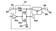
図12において、データ入出力回路215に対し外部からの電源電位VccQを伝達する外部電源配線224と電源線222の間に、入力保護回路(高電圧導通機構)225が設けられる。この電源線222は外部電源端子201に電気的に結合される。
【0086】
データ入出力回路215は、図12においては、出力部が外部電源電位VccQを受ける。大きな負荷を高速で駆動するため、データ出力部が最も消費電流が大きいためである。データ入出力回路215は、内部から読出されたデータを増幅する(レベル変換機能を有してもよい)インバータ回路215aと、電源線224とデータ出力端子215dの間に接続されかつそのゲートにインバータ回路215aの出力信号を受けるnチャネルMOSトランジスタ215bと、データ出力端子215dと接地端子(接地線,接地ノード)204との間に接続されかつそのゲートにインバータ回路215aの出力信号を受けるnチャネルMOSトランジスタ215cを含む。データ出力端子215dには、したがって電源電位VccQレベルのデータまたは接地電位GNDレベルのデータが出力される。データ入出力端子215dに現われるデータ信号の振幅を外部電源電位VccQ(=Vcc)レベルとすることにより、外部に設けられた装置との互換性を保持する。
【0087】
入力保護回路225は、図12においては、寄生npnバイポーラトランジスタで構成されるように示される。電源線224上に過渡高電圧サージが発生したとき、この入力保護回路225に含まれるバイポーラトランジスタが導通し、電源線222上へこの過渡高電圧サージによる電流(電荷)を放電し、この電源線222により高電圧サージを吸収する。電源線222には多くの回路が接続されており、電源線222は大きな浮遊容量を有しており、安定にこの過渡高電圧サージにより生じた電荷を吸収することができる。
【0088】
図13(A)および(B)は、図12に示す入力保護回路の平面レイアウトおよび断面構造を示す図である。図13(A)において、外部電源電位VccQを受ける電源入力パッド202aが、導電配線224aを介して電源線224に接続される。この電源線224と隣接してかつ平行して別の電源線222が配置される。電源線224下部にこの電源線224と平行してフィールド領域234が形成され、また電源線222下部にこの電源線222と平行してフィールド領域232が形成される。フィールド領域232および234は、それぞれコンタクト孔232aおよび234aを介して電源線222および224にそれぞれ接続される。電源線222および224が比較的長距離にわたって平行して配線されているため、フィールド領域232および234の対向する部分の長さを十分に大きくとることができる。これにより、先の実施の形態1ないし3と同様、サージ耐性に優れかつ高速でサージ電流を吸収することのできる入力保護回路を得ることができる。
【0089】
図13(B)は、図13(A)のラインA−A′に沿った断面構造を概略的に示す図である。フィールド領域232は、高濃度n型不純物領域により構成され、フィールド領域234は、高濃度n型不純物領域により構成される。これらのフィールド領域232および234は、p型半導体基板112表面に形成される。フィールド領域232および234の間の基板112の表面上にフィールド絶縁膜239が形成される。フィールド領域234は、第1のノード237に接続されかつフィールド領域232は、第2のノード238に接続される。これらのノード237および238にはそれぞれ電源電位VccQおよびVccが印加される。この図13(A)および(B)の入力保護回路の構成は、先の実施の形態1ないし3に示す高電圧導通機構と同じであり、第1のノード237に電源電位VccQの通常動作時に与えられる電圧レベルよりも高い過渡高電圧サージが印加されたとき、このフィールド領域234、半導体基板112およびフィールド領域232により形成される寄生npnバイポーラトランジスタが導通し(フィールド領域234および232のパンチスルーおよびフィールド領域234の接合の降伏)、高電圧サージがフィールド領域232を介して第2のノード238へ伝達され、また基板112へ伝達されてこの高電圧サージが吸収される。
【0090】
この電源線222は、外部電源電位Vccが伝達される電源線ではなく、内部電源電位Vintが伝達される内部電源線であってもよく、また接地電位GND(出力回路用のGNDQ)が伝達される接地線であってもよい。
【0091】
図14は、図11(B)に示すアレイ周辺回路210aの具体的構成の一例を示す図である。図14において、アレイ周辺回路は、ビット線対BLおよびZBLに対して設けられ、このビット線BLおよびZBLの電位を差動的に増幅するセンスアンプSAと、電源線222a上の外部電源電位Vccを一方動作電源電位として動作し、センスアンプSAを活性化するセンス活性化信号φSPおよびφSNを出力するセンス活性化回路260を含む。ビット線対BLおよびZBLと交差する方向にワード線WLが配置される。ワード線WLとビット線対BLおよびZBLの交差部に対してメモリセルMCが配置される。図14においては、ビット線BLとワード線WLの交差部に配置されるメモリセルMCを代表的に示す。メモリセルMCが行および列のマトリクス状に配設され、メモリセルの各行に対応してワード線WLが配置され、メモリセルの各列に対応してビット線対BLおよびZBLが配置される。メモリセルMCは、情報を格納するキャパシタCMと、ワード線WL上の信号電位に応答して導通してキャパシタCMをビット線BLに電気的に接続するアクセストランジスタMTを含む。
【0092】
センスアンプSAは、ビット線対BLおよびZBLの間に交差結合された1対のnチャネルMOSトランジスタNQと、ビット線対BLおよびZBLの間に互いに交差結合される1対のpチャネルMOSトランジスタPQを含む。このセンスアンプSAに対し、センス活性化回路260からのセンス活性化信号φSPに応答して導通し、電源線222a上の電源電位VccをpチャネルMOSトランジスタPQの接続部へ伝達する活性化トランジスタPTと、センス活性化回路260からのセンス活性化信号φSNに応答して導通して、接地電位GNDを1対のnチャネルMOSトランジスタの接続部へ供給する活性化トランジスタNTを含む。この電源線222aは、ノード201aに接続される。このノード201aは電源パッドであってもよく、また外部ピン端子であってもよい。
【0093】
この図14に示す構成において、センスアンプSAの活性化時、すなわち活性化トランジスタPTおよびNTの導通時、pチャネルMOSトランジスタPQがビット線BLおよびZBLの高電位のビット線を電源電位Vccレベルにまで上昇させ、一方nチャネルMOSトランジスタNQが、低電位のビット線を接地電位GNDレベルにまで放電する。この図14に示す構成においては、ビット線BLおよびZBLの電位振幅は、電源電位Vccレベルとされる。したがってこの図14に示す半導体装置の場合、内部降圧回路は設けられておらず、外部から与えられる電源電位が内部動作電源電位として利用される。センスアンプSAは、ビット線対BLおよびZBLそれぞれに対して設けられる。したがって、センスアンプSAの動作時、多くのビット線BLおよびZBLの充放電が行なわれるため、電源線222aの消費電流は大きくなる。電源線222aの専用の電源ピン端子からノード201aを介して電源電位を供給することにより、安定にセンス動作を行なうことができる。この場合、多くのセンスアンプを駆動するため電源線222aの幅および寄生容量は大きく、サージ吸収用の電源線として用いられても、安定に過渡高電圧サージを吸収することができる。
【0094】
以上のように、この実施の形態4に従えば、外部電源配線と別の一定電位が供給される導電配線との間に高電圧導通機構を設けたため、これらの電源線および導電配線が長距離にわたって平行して並設されるため、容易に高電圧導通機構を配設するための必要十分な面積を確保することができ、何ら占有面積を増加させることなく確実にサージ吸収用の入力保護回路を実現することができる。
【0095】
[実施の形態5]
図15(A)および(B)は、この発明の実施の形態5に従う入力保護回路部分の平面レイアウトおよび断面構造を示す図である。図15(A)において、高電圧導通機構は、電源入力パッド300に導電配線302aを介して接続される電源線302と、この電源線302下部に、電源線302と平行に形成されるフィールド領域312と、フィールド領域312と平行に配設されるフィールド領域314を含む。このフィールド領域314は半導体基板304に電気的に接続される。フィールド領域312は、コンタクト孔312aを介して電源線302に電気的に接続され、またフィールド領域314は、コンタクト孔316aを介してゲート電極層316に接続される。このゲート電極層316は、フィールド領域312および314間の領域にこれらのフィールド領域312および314と平行にかつ電源線302および304より下層に配設される。
【0096】
図15(B)は、図15(A)のラインA−A′に沿った断面構造を示す図である。図15(B)において、p型半導体基板304表面上に、高濃度n型不純物領域で構成されるフィールド領域312と、高濃度p型不純物領域で構成されるフィールド領域314が配設される。これらのフィールド領域312および314の間の基板304表面上に、図示しないゲート絶縁膜を介してゲート電極層316が配設される。このゲート電極層316は、フィールド領域314と電気的に接続される。フィールド領域314および半導体基板304は同じ導電型であり、フィールド領域314は、半導体基板304よりも高不純物濃度を有しており、フィールド領域314は、半導体基板304と電気的に接続される。フィールド領域312は、第1のノード301に電気的に接続される。第1のノード301は、電源入力パッド300または外部電源端子であってもよく、また導電配線302aまたは電源線302の任意の場所であってもよい。半導体基板304は、一定のバイアス電位(接地電位または負電位)Vbを受ける。
【0097】
第1のノード301に過渡高電圧サージが発生した場合、このフィールド領域312のn+/p接合が降伏現象を起こし、半導体基板304表面に沿って、フィールド領域312から、フィールド領域314へ電荷が流れ、このフィールド領域314へ流れ込んだ電荷が、半導体基板304により吸収される。第1のノード301に与えられた高電圧サージが大きいとき、また、このフィールド領域312と半導体基板304の間の接合の降伏現象が生じ、フィールド領域312から基板304へ直接電流が流れる。
【0098】
図15(A)および(B)に示す構成の場合、高電圧導通機構は、その第2のノードが、半導体基板に電気的に接続されている。したがって、電源線302と平行に配設される導電配線(接地線、内部電源線または基準電源線)が存在しない場合においても、この電源線302下部に形成されたフィールド領域312と平行に対向してフィールド領域314を半導体基板304表面に形成することにより、十分な幅を有する高電圧導通機構を実現することができる。したがって、必要とされる配線が存在しない場合においても、容易に必要とされる面積を有する高電圧導通機構を実現することができる。
【0099】
半導体基板304は、十分大きな容量を有しているため、安定に高電圧サージを吸収することができる。またこの電源線302は、任意の形状をとることができるため(第2のノードに接続される導電配線が存在しないため)、必要とされる幅方向の長さをフィールド領域312はとることができ、応じて、電源線302の浮遊容量を十分に大きくすることができ、サージ耐性に優れた入力保護回路を実現することができる。
【0100】
[変更例]
図16は、この発明の実施の形態5の変更例を示す図である。図16に示す構成において、図15(B)に示す構成と異なり、フィールド領域312および314の間の半導体基板304表面に、フィールド絶縁膜317が形成される。このフィールド領域312および314外周にLOCOS膜315aおよび315bが形成される。フィールド領域314に、基板バイアス電位Vd(接地電位または負電位)が印加される。この図16に示す構成においても、第1のノード301に過渡高電圧サージが発生した場合、このフィールド領域312、半導体基板304およびフィールド領域314で形成されるn+/p/p+ダイオードが導通し、第1のノード301に発生した過渡高電圧サージを半導体基板304で吸収することができる。
【0101】
なお、この実施の形態5において、第1のノード301を、p型の不純物領域からなるフィールド領域へ接続し、半導体基板をn型として、このフィールド領域312をn型高濃度不純物領域より形成することにより、この高電圧サージを吸収する保護回路を実現することができる。
【0102】
以上のように、この発明の実施の形態5に従えば、過渡高電圧サージを半導体基板で吸収するように構成したため、電源配線と導電配線が平行して配置されていない領域においても、この電源線を一方ノードとした高電圧導通機構を基板上空き領域を利用して形成することができ、何ら面積増加を伴うことなく必要とされる面積を有する入力保護回路(高電圧導通機構)を実現することができる。
【0103】
[実施の形態6]
図17(A)は、この発明の実施の形態6に従う入力保護回路の要部の構成を示す平面レイアウト図であり、図17(B)は、図17(A)のラインA−A′に沿った断面構造を示す図である。図17(A)において、入力保護回路は、外部から与えられる電源電位Vccを受ける電源入力パッド400と、この電源入力パッド400に導電配線401を介して接続され、外部電源電位Vccを内部へ伝達する外部電源線402と、この外部電源線402と平行してかつ隣接して延在して配置される導電配線404とを含む。この導電配線404は、先の実施の形態4または5と同様、別に設けられた外部電源線、接地線、内部電源線、データ出力部に対して設けられた接地線のいずれであってもよい。動作電源電位としての接地電位GNDまたは電源電位VccまたはVintを伝達する導電配線であればよい。
【0104】
高電圧導通機構は、この電源線402下部に、この電源線402と平行して形成されかつこの電源線402にコンタクト孔(またはバイア孔)414bを介して接続されるフィールド領域412と、導電配線404と平行してこの導電配線404下部に、フィールド領域412と狭い間(約3μm以下)をおいて配置されるフィールド領域414を含む。このフィールド領域414は、コンタクト孔(またはバイア孔)414aを介して導電配線404に接続される。
【0105】
図17(B)において、フィールド領域412および414は、低濃度p型不純物領域で構成されるウェル領域420に形成される。このフィールド領域412および414間のウェル領域420表面に、フィールド絶縁膜417が形成される。フィールド領域412は、高濃度n型不純物領域で構成され、フィールド領域414は、高濃度p型不純物領域で構成される。フィールド領域412は、コンタクト孔414bに形成されたコンタクト402aを介して電源線402に接続される。フィールド領域414は、コンタクト孔414aに形成されたコンタクト404aにより導電線404に接続される。フィールド領域412のコンタクト402aとの接触部の下部に、このフィールド領域412と接して低濃度n型不純物領域で構成される下部ウェル415が形成される。ウェル領域420は、n型半導体基板422表面に形成される。このウェル領域420は、LOCOS膜419aおよび419bにより他の回路部分から分離される。半導体基板422は、外部電源電位Vccまたは接地電位レベルのバイアス電位Vbに固定される。
【0106】
この図17(A)および(B)に示す構成においても、電源線402において過渡高電圧サージが発生した場合、このフィールド領域412とウェル領域420との間の接合の降伏現象(またはフィールド領域間パンチスルー)が生じ、フィールド領域412からウェル領域420を介してフィールド領域414へ電流が流れ、この高電圧サージにより生じた電流が導電配線404により吸収される。またこのとき、フィールド領域412、下部ウェル415、ウェル領域420および半導体基板422により形成されるラテラルnpnバイポーラトランジスタが導通し、この下部ウェル415から、ウェル領域420を介して基板422へ電流が流れ、この高電圧サージが半導体基板422により吸収される。図17(B)においては、下部ウェル415が、寄生バイポーラトランジスタのエミッタ領域を構成するように示される。しかしながら、この寄生バイポーラトランジスタは、過渡高電圧サージ発生時に導通するため、下部ウェル415は、この寄生バイポーラトランジスタのコレクタ領域を形成してもよい。この寄生バイポーラトランジスタのベース領域は、下部ウェル415が設けられているため、その長さが小さくされ、電流増幅率が大きくなり、より多くの電流を、高速で半導体基板422へ流すことができ、高速で高電圧サージを吸収することができる。
【0107】
なお、図17(B)において、示される導電型をすべて逆とすれば、電源線202に代えて、接地線に対する負の高電圧サージに対する保護回路を実現することができる。
【0108】
[変更例]
図18は、この発明の実施の形態6の変更例の構成を示す図である。図18に示す構成においては、フィールド領域414に代えて高濃度n型不純物領域で形成されるフィールド領域424が用いられ、このフィールド領域424とコンタクト404aとの接触部の下部にこのフィールド領域424と接して、低濃度n型不純物領域で構成される下部ウェル422が形成される。すなわち、この図18に示す構成においては、図17に示すn+/pダイオードに代えて、フィールドトランジスタ(ゲート電極はあってもなくてもよい)が高電圧導通機構として用いられる。他の構成は、図17(B)に示す構成と同じである、対応する部分には同一参照番号を付す。
【0109】
この図18に示す構成においては、電源線402において過渡高電圧サージが発生した場合、フィールドトランジスタのパンチスルー現象(寄生バイポーラトランジスタの導通)により、導電配線404により過渡高電圧サージが吸収される。このとき、また下部ウェル415、およびフィールド領域424に対する下部ウェル422を設けることにより、コンタクト404aに対して集中して流れる電流によるフィールド領域424の電界集中およびコンタクト404aの溶融金属の接合の突き抜けをを防止することができ、サージ耐性に優れた入力保護機構を実現することができる。
【0110】
なお、この図18に示す構成においても、寄生バイポーラトランジスタとしては、下部ウェル415および422が、コレクタとして作用しかつ半導体基板422のエミッタとして作用する寄生バイポーラトランジスタが形成されてもよい。また、示される導電型をすべて逆とし、基板バイアス電位を接地電位または負電位とすることにより、接地線に対する負の高電圧サージを吸収する入力保護回路を実現することができる。
【0111】
以上のように、この実施の形態6に従えば、いわゆるトリプルウェル構造を用いて、高電圧サージを半導体基板またはウェル領域で吸収するように構成しているため、ウェル領域および半導体基板の大きな寄生容量に、安定に過渡高電圧サージによる電荷を吸収することができ、サージ耐性に優れた入力保護回路を実現することができる。
【0112】
なお、この実施の形態6においても、フィールドトランジスタに代えてMOSトランジスタが用いられても同様の効果を奏することができる。
【0113】
[実施の形態7]
図19(A)は、この発明の実施の形態7の入力保護回路部分の平面レイアウトを概略的に示す図であり、図19(B)は、図19(A)に示すラインB−B′に沿った断面構造を概略的に示す図である。図19(A)において、外部電源電位Vccを第1のノード504を介して受ける不純物領域500と、この不純物領域500と所定の間隔(約3μm以下)をおいてこの不純物領域500を取り囲むように形成される不純物領域502とが設けられる。この不純物領域500は、高濃度不純物領域(拡散領域)または低濃度不純物領域(ウェル領域)のいずれでもよい。以下の説明においては、不純物領域は、この高濃度不純物領域(拡散領域)および低濃度不純物領域(ウェル領域)両者を示すものとして用いる。
【0114】
不純物領域502は、第2のノード506を介して内部電源電位または接地電位であるバイアス電位Vbに固定される。
【0115】
図19(B)において、不純物領域500が、p型半導体基板512の表面に形成される。この不純物領域500は、n型の導電型を有する。この不純物領域500の両側に、フィールド絶縁膜510aおよび510bを間においてn型不純物領域502aおよび502bが形成される。この不純物領域502aおよび502bは連続的に形成されて、バイアス電位Vbをそれぞれノード506aおよび506bを介して受ける。なお、不純物領域500がウェル領域で構成される場合、第1のノード504に接続する部分は、高濃度不純物領域(拡散領域)で形成される。また、不純物領域502aおよび502bが、ウェル領域で構成される場合、バイアス電位Vbに接続される部分は、高濃度不純物領域(拡散領域)で形成される。
【0116】
この不純物領域502aおよび502bの外周に、LOCOS膜509aおよび509bが形成される。
この図19(A)および(B)に示す構成においても、第1のノード504において過渡高電圧サージが発生した場合、フィールド絶縁膜510aおよび510bの下の領域を介して不純物領域500と不純物領域502aおよび502bとの間にパンチスルー現象(不純物領域500と基板512との間の接合の降伏(ブレークスルー))が生じ、不純物領域500と不純物領域502aおよび502bとが電気的に接続し、過渡高電圧サージが、第2のノード506aを介して吸収される。
【0117】
この図19(A)および(B)に示す構成の場合、何ら電源線および導電配線を互いに平行して配設する必要はなく、半導体基板表面に形成された不純物領域を用いて入力保護回路を形成することができる。また不純物領域500の外周に沿って、不純物領域502が形成されるため、この過渡高電圧サージ電流が流れる領域の幅を十分大きくとることができ、半導体基板表面の、任意の領域において、小占有面積で大きなチャネル幅を有するフィールドトランジスタを等価的に形成することができ、応じて小占有面積でサージ耐性の高い入力保護回路を実現することができる。
【0118】
[変更例1]
図20は、この発明の実施の形態7の変更例1の構成を示す図である。図20においては、断面構造のみが示される。図20においては、不純物領域500の外周に沿って、フィールド絶縁膜510aおよび510bを間において、高濃度p型不純物領域522aおよび522bが形成される。この高濃度p型不純物領域522aおよび522bは、不純物領域500を取り囲むように形成され、したがってその平面レイアウトは図19(A)に示すものと同じとなる。他の構成は、図19(B)に示すものと同じであり、対応する部分には同一の参照番号を付す。
【0119】
この図20に示す構成の場合、不純物領域522aおよび522bは、p型半導体基板512に電気的に接続される。したがって、第1のノード504において過渡高電圧サージが発生した場合、この不純物領域500と不純物領域522aおよび522bの間で接合の降伏現象(またはパンチスルー)が生じて過渡高電圧サージによる電流が不純物領域500から半導体基板512ならびに不純物領域522aおよび522bへ流れかつこれらの不純物領域522aおよび522bから半導体基板512へサージ電流が流れてこの基板512によりサージ電流が吸収される。したがってこの場合においても、半導体基板512は、大きな浮遊容量を有しており、この過渡高電圧サージを安定に吸収することができる。この半導体基板512は、接地電位または負電位または内部電源電位の一定電位にバイアスされていてもよい。
【0120】
[変更例2]
図21(A)は、実施の形態7の変更例2の平面レイアウトを示し、図21(B)は、図21(A)のラインB−B′に沿った断面構造を示す図である。図21(A)において、外部電源電位Vccを第1のノード551を介して受ける不純物領域550の内側に、一定のバイアス電位Vbを第1のノード551を介して受ける不純物領域555が設けられる。すなわち、この変更例2の構成においては、負電位または接地電位または内部電源電位または外部電源電位であるバイアス電位Vbを受ける不純物領域555の外周に沿って、狭い間隔をおいてこの不純物領域555を取り囲むように、外部電源電位Vccを受ける不純物領域550が形成される。
【0121】
図21(B)において、不純物領域555の外側に、フィールド絶縁膜557aおよび557bを間において、不純物領域550aおよび550bが形成される。不純物領域555と不純物領域550aおよび550bの導電型式は、同じであってもよく、また異なっていてもよい。この変更例2の構成においても、第1のノード551において過渡高電圧が発生した場合、パンチスルー現象(または降伏現象)により、不純物領域555および第2のノード556を介して過渡高電圧サージが吸収される。したがって、先の実施の形態7およびその変更例1と同様の小占有面積でサージ耐性に優れた入力保護回路を実現することができる。
【0122】
図22は、この図21(A)の平面レイアウトを実現する部分の具体的構成を示す図である。図22において、不純物領域550は、外部電源電位Vccを使用する回路部分が形成されるVcc使用回路形成領域550cと、このVcc使用回路形成領域550cの外部電源電位Vcc印加領域(拡散領域またはウェル領域)と電気的に接続される不純物領域550dにより、不純物領域550が形成される。この不純物領域550dには、内部回路要素は形成されていなくてもよい。さらに、Vcc使用回路形成領域550cも、外部電源電位Vcc印加領域と電気的に接続されていればよく、したがって、不純物領域550aは、拡散領域であってもよく、またウェル領域であってもよい。この場合、不純物領域555にはバイアス電位Vbが印加され、この領域において別の内部回路構成要素が形成されていてもよい。この場合、回路構成要素形成領域に沿って、入力保護回路を形成することができて何ら占有面積を増加させることなく、また、レイアウトの変更を生じることなく、容易に十分なレイアウト面積を有する入力保護回路を形成することができ、サージ耐性に優れた入力保護回路を実現することができる。
【0123】
以上のように、この実施の形態7に従えば、外部電源電位が印加される領域と、これと過渡高電圧サージ吸収部に電気的に接続される領域とを設けかつ、一方が他方を取り囲むように構成したため、少ない占有面積でかつ電源配線の配設されていない領域においても、容易に十分なレイアウト面積を有する入力保護回路を形成することができ、サージ耐性に優れた入力保護回路を実現することができる。
【0124】
[実施の形態8]
図23(A)は、この発明の実施の形態8に従う半導体装置のチップレイアウトを示す図であり、図23(B)は、図23(A)のラインA−A′に沿った断面構造を概略的に示す図であり、図23(C)は、図23(A)のラインB−B′に沿った断面構造を概略的に示す図である。
【0125】
図23(A)において、半導体装置が形成されるチップ600外周に沿って、導電配線602が配設される。この導電配線602は、後に説明するように、このチップ600の構成する半導体基板と電気的に接続される。半導体基板は、基準電位発生手段からの基準電位を受ける。この基準電位発生手段は、半導体基板が、p型基板の場合には、負電位Vbbを発生する負電位発生回路かまたは、接地電位GNDを供給する接地線である。
【0126】
この導電配線602は、外部からの電源電位が印加される電源パッド604に入力保護回路606を介して結合される。この入力保護回路606の具体的構成は、実施の形態1ないし7のいずれであってもよい。
【0127】
図23(B)において、半導体チップ600を構成するp型半導体基板605の表面に、高濃度p型不純物領域606が形成される。この不純物領域606は、コンタクト607を介して導電配線602に接続される。不純物領域606は、半導体基板605と同じ導電型であり、したがってこの不純物領域606と半導体基板605とは電気的に接続される。したがって、導電配線602は、この不純物領域606を介して半導体基板605に電気的に接続される。
【0128】
図23(C)において、入力保護回路606は、電源パッド604に接続される導電配線(第1のノード)619と、半導体基板605表面に形成され、かつコンタクト617を介して導電配線619に接続される高濃度n型不純物領域611と、この高濃度n型不純物領域611とコンタクト617との接触部の下部に、この不純物領域611に接して形成される低濃度n型不純物領域(下部ウェル)612と、半導体基板605表面に形成されかつコンタクト618を介して導電配線602に接続される高濃度n型不純物領域614を含む。これらの不純物領域611および614、すなわちフィールド領域611および614の間に、フィールド絶縁膜616が形成される。フィールド領域611および614の幅は、十分大きくかつ両者間の距離は十分小さくされる。
【0129】
導電配線602は、半導体基板605表面に形成された高濃度p型不純物領域606にコンタクト619を介して接続される。このフィールド(不純物)領域614と高濃度不純物領域606の間に、LOCOS膜615が形成される。
【0130】
チップ600の外周に沿って配設される導電配線602は、十分な長さおよび幅を有している。したがってこの導電配線602の浮遊容量は十分大きく、ノード619において発生した過渡高電圧サージを、確実に吸収することができる。また、この導電配線602は、一定電位に固定された半導体基板605に不純物領域606を介して接続されているため、この導電配線602上に生じた電荷は、半導体基板605により吸収され、導電配線602の電位の変動は確実に防止することができる。
【0131】
なお、この実施の形態8において、フィールド領域611は、高濃度不純物領域でなく、外部電源電位Vccが印加されるウェル領域であってもよい。また、不純物領域606は、チップ外周部全体に沿って形成される必要はなく、チップ600の適当な箇所において導電配線602と接続されていればよい。
【0132】
この実施の形態8の構成に従えば、不純物領域611および612の上部に両領域611および612と平行して電源線または導電配線を配設する必要はない。過渡高電圧サージを瞬時に吸収することのできる幅(図23(C)の紙面垂直方向)を、不純物領域611および614ならびに不純物領域614上に形成されかつ導電配線602に接続される配線部分が有していればよい。何ら占有面積を増加せずチップ外周部の空き領域において、外部電源電位が供給される領域近傍に入力保護回路を配設することができ、小占有面積かつサージ耐性に優れた入力保護回路を実現することができる。
【0133】
[実施の形態9]
図24(A)は、この発明の実施の形態9の入力保護回路の平面レイアウトを示し、図24(B)は、図24(A)のラインA−A′に沿った断面構造を概略的に示す図である。図24(A)において、高電圧導通機構は、外部の電源電位Vccを第1のノード701を介して受ける不純物領域702と、この不純物領域702に隣接してかつ間をおいて配置される不純物領域703とを含む。不純物領域702は、外部電源電位Vccを使用する回路要素が形成される領域の拡散領域またはウェル領域である。不純物領域703は、内部電源電位Vint、接地電位などを使用する回路要素の形成される拡散領域またはウェル領域である。この不純物領域702および703の境界部に高電圧印加時に導通する部分が形成される。
【0134】
図24(B)において、不純物領域702は、高濃度n型不純物領域で形成されかつコンタクト705を介して外部電源電位Vccを受ける第1のノードとなる導電配線701に接続される。この不純物領域702下部に、低濃度n型不純物領域で形成される下部ウェル704が形成される。この下部ウェル704は、少なくともコンタクト705と不純物領域702との接触部下部に形成される。不純物領域703は、p型半導体基板700表面に形成される低濃度n型ウェル領域706と、このウェル領域706表面に形成される高濃度n型不純物領域707を含む。高濃度不純物領域707は、コンタクト708を介して、内部電源Vintなどの固定電位を伝達する導電配線709に接続される。不純物領域702とウェル領域706の間は十分小さくされ、過渡高電圧サージ発生時においてこの不純物領域702とウェル領域706との間でパンチスルーが生じるようにされる。不純物領域702とウェル領域706の間にLOCOS酸化膜710bが形成され、不純物領域702および707外周部に沿ってLOCOS膜710aおよび710cが形成される。
【0135】
nウェル領域706は、不純物領域707と電気的に接続されており、導電線(第2のノード)709を介して与えられる内部電源電位Vintまたは接地電位である固定電位に固定される。このウェル領域706内に、内部電源電位Vintなどの固定電位を使用する回路が形成される。第1のノード701において過渡高電圧サージが発生した場合、不純物領域702とウェル領域706の間でパンチスルー現象が生じ、この過渡高電圧サージは、不純物領域702からウェル領域706へ流れ、次いで不純物領域707を介して第2のノード709へ流れて、この第2のノード709に接続される固定電位発生手段により吸収される。したがってこの実施の形態9の構成においても、確実に過渡高電圧サージを吸収することができる。また、外部電源配線および内部電源配線などの電源電位を伝達する導電配線を互いに平行して長距離にわたって配設する必要がなく、回路レイアウトの自由度が増加する。また、不純物領域702および703が長距離にわたって平行して配設されているため、この高電圧導通機構のチャネル幅(ラインA−A′の直角方向)は十分大きくでき、応じてサージ耐性に優れた入力保護回路を実現することができる。
【0136】
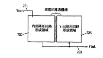
図25は、不純物領域702および703に形成される回路構成要素の具体例を示す図である。図25において、第2のノード721に与えられる外部電源電位Vccを変換して内部電源電位Vintを生成する内部降圧回路の形成領域720と、これと隣接して、この内部電源電位Vintを内部電源線723を介して受けて動作するVint使用回路の形成領域725とが設けられる。内部降圧回路形成領域720においては、先に図2において示したように、ドライブトランジスタは、pチャネルMOSトランジスタで構成される。また、比較回路105も、カレントミラー型回路の場合、カレントミラー回路はpチャネルMOSトランジスタで構成される。このようなpチャネルMOSトランジスタが外部電源電位Vccを一方導通ノードに受けるため、このpチャネルMOSトランジスタが形成されるn型ウェル領域が、外部電源電位Vccにバイアスされる。したがってこのウェル領域を図24(A)に示す不純物領域702として用いる。内部電源電位Vint使用回路は、これを内部電源電位Vintを使用して動作する。この場合、pチャネルMOSトランジスタが形成される領域が、同様、n型ウェル領域である。このn型ウェル領域は、したがって内部電源電位Vintにバイアスされる。これらのウェル領域を、図24(A)に示す不純物領域702および703として使用することにより、図25において斜線部で示す高電圧導通機構を容易に実現することができる。
【0137】
なお、領域720が、データ出力回路形成領域であり、また領域725は、内部読出データを増幅してデータ出力回路へ与えるプリアンプなどの内部データ読出回路の形成領域であってもよい。
【0138】
以上のように、この実施の形態9に従えば、外部電源電位を使用する領域に隣接して内部電源電位等の固定電位を使用する回路領域を配置し、これらの境界領域を高電圧導通機構として利用したため、十分な幅を有する高電圧導通機構を形成することができ、小占有面積で、サージ耐性に優れた入力保護回路を実現することができる。また、単に回路構成要素形成領域を利用しているため、入力保護機構のための専用の領域を設ける必要がなく、レイアウトが容易となる。
【0139】
なお、実施の形態1ないし9において、不純物領域の導電型を逆とすれば、外部電源電位に代えて接地電位に対する負の高電圧サージを吸収する機構を実現することができる。
【0140】
【発明の効果】
以上のように、この発明に従えば、サージ吸収のための高電圧導通機構として、固定電位伝達線または回路形成領域を利用しているため、何ら入力保護機構のための専用の領域を設ける必要がなく、小占有面積でかつサージ耐性に優れた入力保護回路を実現することができる。
【図面の簡単な説明】
【図1】この発明の実施の形態1の半導体装置の全体の構成を概略的に示す図である。
【図2】図1に示す内部降圧回路の構成の一例を示す図である。
【図3】(A)は、図1に示す高電圧導通機構の平面レイアウトを示し、(B)は、(A)のラインA−A′に沿った断面構造を概略的に示す図である。
【図4】(A)は、実施の形態2の平面レイアウトを示し、(B)は、(A)のラインA−A′に沿った断面構造を概略的に示す図である。
【図5】この発明の実施の形態2の変更例1の構成を示す図である。
【図6】この発明の実施の形態2の変更例2の構成を示す図である。
【図7】(A)は、この発明の実施の形態3の入力保護回路の平面レイアウトを示し、(B)は、(A)のラインA−A′に沿った断面構造を概略的に示す図である。
【図8】この発明の実施の形態3の変更例1の構成を概略的に示す図である。
【図9】この発明の実施の形態3の変更例2の構成を概略的に示す図である。
【図10】この発明の実施の形態3の変更例3の構成を概略的に示す図である。
【図11】(A)は、この発明の実施の形態4に従う半導体記憶装置の全体の構成を概略的に示し、(B)は、(A)に示す配置における電源線のレイアウトを示す図である。
【図12】この発明の実施の形態3に従う入力保護回路の構成を具体的に示す図である。
【図13】図12に示す高電圧導通機構の平面レイアウトおよび断面構造を概略的に示す図である。
【図14】この発明の実施の形態3の変更例の構成を示す図である。
【図15】(A)は、この発明の実施の形態4に従う入力保護回路の平面レイアウトを示し、(B)は、(A)のラインA−A′に沿った断面構造を概略的に示す図である。
【図16】この発明の実施の形態5の変更例の構成を概略的に示す図である。
【図17】(A)は、この発明の実施の形態6に従う入力保護回路の平面レイアウトを概略的に示し、(B)は、(A)のラインA−A′に沿った断面構造を概略的に示す図である。
【図18】この発明の実施の形態6の変更例の構成を概略的に示す図である。
【図19】(A)は、この発明の実施の形態7の入力保護回路の平面レイアウトを示し、(B)は、(A)のラインB−B′に沿った断面構造を概略的に示す図である。
【図20】この発明の実施の形態7の変更例1の構成を概略的に示す図である。
【図21】(A)は、この発明の実施の形態7の変更例1の平面レイアウトを示し、(B)は、(A)のラインB−B′に沿った断面構造を概略的に示す図である。
【図22】この発明の実施の形態7の変更例2の構成を概略的に示す図である。
【図23】(A)は、この発明の実施の形態8に従う入力保護回路のチップレイアウトを示し、(B)は、(A)のラインA−A′に沿った断面構造を示し、(C)は、ラインB−B′に沿った断面構造を概略的に示す図である。
【図24】(A)は、この発明の実施の形態9に従う入力保護回路の平面レイアウトを示し、(B)は、(A)のラインA−A′に沿った断面構造を概略的に示す図である。
【図25】図24に示される不純物領域が形成される回路の具体例を示す図である。
【図26】(A)は、従来の入力保護回路の平面レイアウトを示し、(B)は、(A)のラインA−A′に沿った断面構造を概略的に示す図である。
【図27】従来の外部電源線と内部電源線のレイアウトを概略的に示す図である。
【図28】従来の半導体記憶装置における電源線のレイアウトを概略的に示す図である。
【符号の説明】
101 外部電源端子、102 外部電源線、105 内部降圧回路、106内部電源線、110 高電圧導通機構、120,122 フィールド領域、126 ゲート電極層、124 フィールド絶縁膜、142,144 フィールド領域(不純物領域)、145,146 下部ウェル、112 半導体基板、147 ゲート電極層、152,154 フィールド領域(不純物領域)、155,156 下部ウェル、114 半導体基板、116 ウェル領域、201 外部電源端子、202 データ出力用電源端子、215 データ入出力回路、222内部回路用電源線、224 データ出力用電源線、225 入力保護回路、232,234 フィールド領域、260 センス活性化回路、302 外部電源線、304 導電配線、312,314 フィールド領域、304 半導体基板、317 フィールド絶縁膜、402 外部電源線、404 導電配線、412,414 フィールド領域、420 ウェル領域、415 下部ウェル、422半導体基板、423 下部ウェル、500 外部電源電位印加領域、502固定電位印加領域、500,502a,502b 不純物領域、510a,510b フィールド絶縁膜、512 半導体基板、522a,522b 不純物領域、550 外部電源電位印加領域、555 固定電位印加領域、550c、外部電源電位使用回路形成領域、550d 不純物領域、600 半導体チップ、601 高電圧導通機構、602 導電配線、605 半導体基板、606 不純物領域、611,614 不純物領域、612 下部ウェル、702 外部電源電位印加領域、703 固定電位印加領域、706 ウェル領域、700 半導体基板、720 内部降圧回路形成領域、725 内部電源電位使用回路形成領域。[0001]
TECHNICAL FIELD OF THE INVENTION
The present invention relates to an input protection circuit for protecting an internal circuit from a transient high-voltage surge externally applied to a power input terminal and a signal input / output terminal of a semiconductor device, and more particularly to an input protection circuit applied to a power input terminal of a semiconductor integrated circuit. The present invention relates to a configuration for protecting an internal circuit from a high voltage surge.
[0002]
[Prior art]
FIG. 26 is a diagram showing a layout and a sectional structure of a power supply input portion of a conventional semiconductor device, for example, a dynamic random access memory. In FIG. 26A, a power supply voltage Vcc is externally applied to power
[0003]
In regions where
[0004]
In FIG. 26B,
[0005]
The
[0006]
[0007]
When a transient high voltage surge is applied to the
[0008]
By providing the input protection circuit for the power supply input pad as described above, a high voltage is prevented from being applied to a circuit using the power supply potential Vcc applied to the power
[0009]
[Problems to be solved by the invention]
When a transient high voltage surge is applied, it is necessary to absorb the high voltage surge at high speed. In order to discharge a high voltage surge from
[0010]
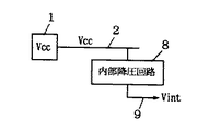
In a recent semiconductor memory device, as shown in FIG. 27, external power supply potential Vcc applied to power
[0011]
In addition, in order to stabilize the operation of the internal circuit, as shown in FIG. 28, circuit portions of the semiconductor memory device are grouped, and a power input pad is separately provided for each group.
[0012]
In FIG. 28, a semiconductor memory device (dynamic random access memory) includes an
[0013]
The
[0014]
In the structure shown in FIGS. 27 and 28, power
[0015]
When a high voltage surge is input, the surge application period is relatively short, and a large amount of charge is supplied within the short period. When a constant charge is supplied as a surge when the wiring stray capacitance of the
[0016]
Since the lengths of
[0017]
SUMMARY OF THE INVENTION It is therefore an object of the present invention to provide an input protection circuit that can easily improve surge resistance of external terminals, particularly power supply input terminals, without increasing the chip size.
[0021]
The input protection circuit according to
The high voltage conduction mechanism includes a first impurity region formed on the surface of the semiconductor substrate region and connected to the first node, and a first impurity region on the surface of the semiconductor substrate region adjacent to and between the first impurity region. And a second impurity region further electrically connected to the second node. The first impurity region has a first conductivity type, and the semiconductor substrate region and the second impurity region have a second conductivity type different from the first conductivity type.
[0035]
[Means for Solving the Problems]
Claim1Input power supply circuit receives an externally supplied power supply voltage and transmits the same to the inside, and converts the external power supply voltage supplied from the external power supply node to generate an internal power supply voltage at the internal power supply node Internal power supply voltage generating means, a first node coupled to the external power supply node, and a second node coupled to the internal power supply node. A high-voltage conduction mechanism that conducts when a voltage higher than the voltage is applied to electrically connect the first node and the second node;
The high-voltage conduction mechanism is arranged on a first substrate region connected to the first node and on which a circuit element using an external power supply voltage is formed, and adjacent to and spaced from the substrate region in a planar layout. And a diffusion region connected to the second node.
The circuit element formed in the substrate region includes an internal power supply potential generating means for generating an internal power supply voltage from the external power supply voltage. The diffusion region is electrically connected to a region where a circuit utilizing the internal power supply voltage is formed.
[0036]
Claim2The input protection circuit according to the claim1Is formed so as to surround the substrate region.
[0037]
Claim3In the input protection circuit according to the first aspect, the diffusion region according to
An input protection circuit according to a fourth aspect of the present invention is the input protection circuit according to the first aspect, further comprising: a wiring electrically connected to the first node; a contact electrically connecting the wiring to the first substrate region; In the contact region, an impurity region having the same conductivity type and a low impurity concentration as the first substrate region formed below the first substrate region is provided.
[0040]
By using a conductive line to which a fixed potential is provided in parallel with the vicinity of the external power supply line for a node to which an external power supply potential is applied, the power supply line and the ground line are different from the related art. It is not necessary to provide an input protection circuit only in the juxtaposed portion, and a required area can be easily secured, and accordingly, an input protection circuit having excellent surge resistance can be realized.
[0041]
BEST MODE FOR CARRYING OUT THE INVENTION
[Embodiment 1]
FIG. 1 schematically shows an entire configuration of a semiconductor device according to the first embodiment of the present invention. In FIG. 1, a
[0042]
[0043]
Therefore, high
[0044]
FIG. 2 is a diagram showing a detailed configuration of internal voltage down
[0045]
A transient high-voltage surge (pulse-like high-voltage noise having a KV order) having a voltage level higher than a normal potential level (for example, 3.3 V) of external power supply potential Vcc is applied to external
[0046]
FIG. 3 is a diagram showing the configuration of the high-voltage conduction mechanism shown in FIGS. 1 and 2 in more detail. In FIG. 3A, external
[0047]
The high
[0048]
FIG. 3B is a diagram showing a cross-sectional structure along the line AA ′ shown in FIG. In FIG. 3B,
[0049]
On the surface of
[0050]
As shown in FIG. 3A, the external
[0051]
In the first embodiment, an input protection circuit similar to the conventional one may be provided in a region where external
[0052]
As described above, according to the first embodiment of the present invention, the external power supply line and the internal power supply line are electrically connected when a transient high voltage is applied to the external power supply line. Since the internal power supply lines are arranged in parallel over a long distance, a field area having a sufficient width can be easily formed, and the input protection has excellent surge resistance and can reliably absorb a transient high voltage surge. A circuit can be obtained.
[0053]
[Embodiment 2]
FIGS. 4A and 4B show a planar layout and a sectional structure of an input protection circuit portion according to the second embodiment of the present invention. In FIG. 4A, the high-
[0054]
[0055]
FIG. 4B is a diagram showing a cross-sectional structure along line AA ′ shown in FIG. In FIG. 4B, similarly to the first embodiment,
[0056]
Also in the configuration shown in FIGS. 4A and 4B, when a transient high voltage surge occurs at the first node, punch-through occurs in the short channel region below
[0057]
As shown in FIGS. 4A and 4B, as a high-voltage conduction mechanism, a short-channel ordinary MOS transistor (the gate insulating film needs to be relatively thick to maintain its breakdown voltage characteristics). Even when used, as in the first embodiment, the transient high voltage surge generated at the first node causes the internal power supply via the
[0058]
[Modification 1]
FIG. 5 is a diagram showing a configuration of a first modification of the second embodiment of the present invention. In FIG. 5, a high-
In the configuration shown in FIG. 5, when a transient high voltage surge is applied to the first node, a breakdown phenomenon occurs at the n + / p junction between
[0059]
At this time, a vertical npn parasitic bipolar transistor is formed by
[0060]
[Modification 2]
FIG. 6 is a diagram showing a configuration of a second modification of the second embodiment of the present invention. In the configuration shown in FIG. 6, a p-type impurity is implanted at a high concentration into
[0061]
By implanting p-type impurity ions at a high concentration into
[0062]
In the
[0063]
As described above, according to the second embodiment of the present invention, an MOS transistor or an n + / p junction is used as an input protection mechanism instead of a field transistor. This transient high voltage surge can be absorbed by the punch-through phenomenon of the transistor (the ON state of the parasitic bipolar transistor) or the breakdown phenomenon of the n / p junction, and the internal circuit can be reliably protected.
[0064]
[Embodiment 3]
FIG. 7A shows a planar layout of the input protection circuit according to the third embodiment of the present invention, and FIG. 7B shows a cross-sectional structure taken along line AA 'of FIG. 7A. It is.
[0065]
In FIG. 7A, the high-voltage conduction mechanism is provided with an external
[0066]
In FIG. 7B,
[0067]
The
[0068]
When a transient high voltage surge occurs in the external
[0069]
Further, when a large current flows from the
[0070]
By providing lower well 146 also for
[0071]
[Modification 1]
FIG. 8 is a diagram showing a configuration of a first modification of the third embodiment of the present invention. In the configuration shown in FIG. 8, a MOS transistor is used instead of a field transistor. That is, the
[0072]
In the configuration shown in FIG. 8, when a transient high voltage surge occurs in external
[0073]
In the structure shown in FIG. 8, lower well 145 may be formed even below
[0074]
[Modification 2]
FIG. 9 shows a configuration of a second modification of the third embodiment of the present invention. In the structure shown in FIG. 9, p-
[0075]
In the configuration shown in FIG. 9, by providing lower well 145, the distance between lower well 145 and n-
[0076]
[Modification 3]
FIG. 10 is a diagram showing a configuration of a third modification of the third embodiment of the present invention. In FIG. 10,
[0077]
In the case of the configuration shown in FIG. 10, when a negative high voltage surge occurs in
[0078]
Also in the configuration shown in FIG. 10, even if a large current flows and the contact melts, it is possible to prevent the molten metal from diffusing into
[0079]
In the structure shown in FIG. 10,
[0080]
As described above, according to the third embodiment, the well region (impurity region) having a low impurity concentration is provided below the contact of the field region connected to the power supply line via the contact. Even when a large current is generated, it is possible to prevent the junction breakdown in the field region, and it is possible to obtain an input protection circuit having high surge resistance.
[0081]
[Embodiment 4]
FIG. 11 schematically shows a configuration of a semiconductor device according to the fourth embodiment of the present invention. 11A, a
[0082]
A dedicated
[0083]
FIG. 11B shows an arrangement of power supply pads inside the semiconductor device. FIG. 11B shows an example of a pad arrangement of a so-called LOC (lead-on-chip) structure.
[0084]
As shown in FIG. 11B, even when such
[0085]
In FIG. 12, an input protection circuit (high-voltage conduction mechanism) 225 is provided between
[0086]
In FIG. 12, data input /
[0087]
In FIG. 12,
[0088]
FIGS. 13A and 13B are diagrams showing a planar layout and a sectional structure of the input protection circuit shown in FIG. In FIG. 13A, power
[0089]
FIG. 13B is a diagram schematically showing a cross-sectional structure along line AA ′ in FIG.
[0090]
[0091]
FIG. 14 is a diagram illustrating an example of a specific configuration of the array
[0092]
Sense amplifier SA includes a pair of n-channel MOS transistors NQ cross-coupled between bit line pairs BL and ZBL, and a pair of p-channel MOS transistors PQ cross-coupled between bit line pairs BL and ZBL. including. Activation transistor PT which conducts to sense amplifier SA in response to sense activation signal φSP from
[0093]
In the configuration shown in FIG. 14, when sense amplifier SA is activated, that is, when activation transistors PT and NT are turned on, p-channel MOS transistor PQ sets the high potential bit lines of bit lines BL and ZBL to power supply potential Vcc level. While the n-channel MOS transistor NQ discharges the low potential bit line to the level of the ground potential GND. In the configuration shown in FIG. 14, the potential amplitudes of bit lines BL and ZBL are at the level of power supply potential Vcc. Therefore, in the case of the semiconductor device shown in FIG. 14, an internal step-down circuit is not provided, and a power supply potential applied from the outside is used as an internal operation power supply potential. Sense amplifier SA is provided for each of bit line pairs BL and ZBL. Therefore, during the operation of sense amplifier SA, many bit lines BL and ZBL are charged and discharged, so that the power consumption of
[0094]
As described above, according to the fourth embodiment, the high-voltage conduction mechanism is provided between the external power supply wiring and the conductive wiring to which another constant potential is supplied. The input protection circuit for surge absorption can be ensured without increasing the occupied area because it is possible to easily secure the necessary and sufficient area for arranging the high-voltage conduction mechanism. Can be realized.
[0095]
[Embodiment 5]
FIGS. 15A and 15B show a plane layout and a sectional structure of an input protection circuit portion according to the fifth embodiment of the present invention. In FIG. 15A, a high-voltage conduction mechanism includes a
[0096]
FIG. 15B is a diagram showing a cross-sectional structure along a line AA ′ in FIG. In FIG. 15B, a
[0097]
When a transient high voltage surge occurs at the
[0098]
In the case of the structure illustrated in FIGS. 15A and 15B, the second node of the high-voltage conduction mechanism is electrically connected to the semiconductor substrate. Therefore, even when there is no conductive wiring (ground line, internal power supply line, or reference power supply line) provided in parallel with
[0099]
Since the
[0100]
[Example of change]
FIG. 16 shows a modification of the fifth embodiment of the present invention. In the structure shown in FIG. 16, a
[0101]
In the fifth embodiment,
[0102]
As described above, according to the fifth embodiment of the present invention, since the semiconductor substrate is configured to absorb the transient high voltage surge, even in a region where the power supply wiring and the conductive wiring are not arranged in parallel, this power supply A high-voltage conduction mechanism with a line as one node can be formed using the empty area on the board, and an input protection circuit (high-voltage conduction mechanism) with the required area without any increase in area is realized. can do.
[0103]
FIG. 17A is a plan layout diagram showing a configuration of a main portion of the input protection circuit according to the sixth embodiment of the present invention, and FIG. 17B is a diagram showing a configuration of line AA ′ in FIG. It is a figure which shows the cross-sectional structure along. In FIG. 17A, an input protection circuit includes a power
[0104]
A high-voltage conduction mechanism is formed below the
[0105]
In FIG. 17B,
[0106]
Also in the configuration shown in FIGS. 17A and 17B, when a transient high voltage surge occurs on
[0107]
Note that in FIG. 17B, if all the conductivity types shown are reversed, a protection circuit against a negative high-voltage surge on the ground line can be realized instead of the
[0108]
[Example of change]
FIG. 18 shows a configuration of a modification of the sixth embodiment of the present invention. In the structure shown in FIG. 18, a field region 424 formed of a high-concentration n-type impurity region is used in place of
[0109]
In the configuration shown in FIG. 18, when a transient high voltage surge occurs in
[0110]
In the structure shown in FIG. 18 as well, a parasitic bipolar transistor in which
[0111]
As described above, according to the sixth embodiment, a so-called triple well structure is used to absorb a high voltage surge in the semiconductor substrate or the well region. It is possible to stably absorb the charge due to the transient high voltage surge in the capacitance, and to realize an input protection circuit having excellent surge resistance.
[0112]
In the sixth embodiment, the same effect can be obtained even if a MOS transistor is used instead of the field transistor.
[0113]
FIG. 19A is a diagram schematically showing a planar layout of an input protection circuit portion according to the seventh embodiment of the present invention, and FIG. 19B is a diagram showing a line BB ′ shown in FIG. FIG. 3 is a drawing schematically showing a cross-sectional structure along the line. Referring to FIG. 19A,
[0114]
[0115]
In FIG. 19B,
[0116]
LOCOS
Also in the configuration shown in FIGS. 19A and 19B, when a transient high voltage surge occurs at
[0117]
In the structure shown in FIGS. 19A and 19B, it is not necessary to arrange the power supply line and the conductive line at all in parallel with each other, and the input protection circuit is formed by using the impurity region formed on the surface of the semiconductor substrate. Can be formed. Further, since
[0118]
[Modification 1]
FIG. 20 is a diagram showing a configuration of a first modification of the seventh embodiment of the present invention. FIG. 20 shows only the cross-sectional structure. 20, high-concentration p-
[0119]
In the configuration shown in FIG. 20,
[0120]
[Modification 2]
FIG. 21A shows a planar layout of a second modification of the seventh embodiment, and FIG. 21B is a diagram showing a cross-sectional structure along line BB ′ of FIG. 21A. In FIG. 21A,
[0121]
In FIG. 21B,
[0122]
FIG. 22 is a diagram showing a specific configuration of a portion for realizing the planar layout of FIG. In FIG. 22,
[0123]
As described above, according to the seventh embodiment, the region to which the external power supply potential is applied and the region electrically connected to the region and the transient high-voltage surge absorbing portion are provided, and one surrounds the other. With this configuration, it is possible to easily form an input protection circuit with a sufficient layout area even in an area with a small occupied area and no power wiring, realizing an input protection circuit with excellent surge resistance. can do.
[0124]
FIG. 23A shows a chip layout of the semiconductor device according to the eighth embodiment of the present invention, and FIG. 23B shows a cross-sectional structure taken along line AA 'of FIG. FIG. 23C is a diagram schematically showing a cross-sectional structure taken along line BB ′ in FIG. 23A.
[0125]
In FIG. 23A, a
[0126]
This
[0127]
In FIG. 23B, a high-concentration p-
[0128]
In FIG. 23C, an
[0129]
The
[0130]
The
[0131]
In the eighth embodiment,
[0132]
According to the structure of the eighth embodiment, it is not necessary to dispose a power supply line or a conductive wiring above
[0133]
Embodiment 9
FIG. 24A shows a planar layout of the input protection circuit according to the ninth embodiment of the present invention, and FIG. 24B schematically shows a cross-sectional structure taken along line AA 'of FIG. FIG. 24A, a high-voltage conduction mechanism includes an
[0134]
In FIG. 24B,
[0135]
N well
[0136]
FIG. 25 is a diagram showing a specific example of a circuit component formed in
[0137]
[0138]
As described above, according to the ninth embodiment, a circuit region using a fixed potential such as an internal power supply potential is arranged adjacent to a region using an external power supply potential, and these boundary regions are connected to a high-voltage conduction mechanism. Therefore, a high-voltage conduction mechanism having a sufficient width can be formed, and an input protection circuit having a small occupation area and excellent in surge resistance can be realized. Further, since the circuit component forming area is simply used, there is no need to provide a dedicated area for the input protection mechanism, and the layout is facilitated.
[0139]
In
[0140]
【The invention's effect】
As described above, according to the present invention, since a fixed potential transmission line or a circuit forming region is used as a high voltage conduction mechanism for absorbing surge, it is necessary to provide a dedicated area for an input protection mechanism. Therefore, an input protection circuit having a small occupied area and excellent in surge resistance can be realized.
[Brief description of the drawings]
FIG. 1 is a diagram schematically showing an overall configuration of a semiconductor device according to a first embodiment of the present invention;
FIG. 2 is a diagram showing an example of a configuration of an internal voltage down converter shown in FIG. 1;
FIG. 3A is a plan view showing a plan layout of the high-voltage conduction mechanism shown in FIG. 1, and FIG. 3B is a view schematically showing a cross-sectional structure taken along line AA ′ of FIG. .
FIG. 4A is a diagram illustrating a planar layout according to a second embodiment, and FIG. 4B is a diagram schematically illustrating a cross-sectional structure taken along line AA ′ of FIG.
FIG. 5 is a diagram showing a configuration of a first modification of the second embodiment of the present invention.
FIG. 6 is a diagram showing a configuration of a second modification of the second embodiment of the present invention.
FIG. 7A shows a planar layout of an input protection circuit according to a third embodiment of the present invention, and FIG. 7B schematically shows a cross-sectional structure taken along line AA ′ of FIG. FIG.
FIG. 8 is a diagram schematically showing a configuration of a first modification of the third embodiment of the present invention;
FIG. 9 is a diagram schematically showing a configuration of a second modification of the third embodiment of the present invention.
FIG. 10 is a diagram schematically showing a configuration of a third modification of the third embodiment of the present invention;
FIG. 11A schematically shows an entire configuration of a semiconductor memory device according to a fourth embodiment of the present invention, and FIG. 11B shows a layout of power supply lines in the arrangement shown in FIG. is there.
FIG. 12 is a diagram specifically showing a configuration of an input protection circuit according to a third embodiment of the present invention.
13 is a diagram schematically showing a planar layout and a cross-sectional structure of the high-voltage conduction mechanism shown in FIG.
FIG. 14 is a diagram showing a configuration of a modification of the third embodiment of the present invention.
FIG. 15A shows a planar layout of an input protection circuit according to a fourth embodiment of the present invention, and FIG. 15B schematically shows a cross-sectional structure taken along line AA ′ of FIG. FIG.
FIG. 16 schematically shows a configuration of a modification of the fifth embodiment of the present invention.
FIG. 17A schematically shows a planar layout of an input protection circuit according to a sixth embodiment of the present invention, and FIG. 17B schematically shows a cross-sectional structure taken along line AA ′ of FIG. FIG.
FIG. 18 is a diagram schematically showing a configuration of a modification of the sixth embodiment of the present invention.
FIG. 19A shows a planar layout of an input protection circuit according to a seventh embodiment of the present invention, and FIG. 19B schematically shows a cross-sectional structure along line BB ′ of FIG. FIG.
FIG. 20 schematically shows a configuration of a first modification of the seventh embodiment of the present invention.
FIG. 21A shows a planar layout of a first modification of the seventh embodiment of the present invention, and FIG. 21B schematically shows a cross-sectional structure along line BB ′ of FIG. FIG.
FIG. 22 is a drawing illustrating roughly configuration of
23A shows a chip layout of an input protection circuit according to an eighth embodiment of the present invention, FIG. 23B shows a cross-sectional structure along line AA ′ of FIG. 23A, and FIG. () Is a diagram schematically showing a cross-sectional structure along line BB '.
FIG. 24A shows a planar layout of an input protection circuit according to a ninth embodiment of the present invention, and FIG. 24B schematically shows a sectional structure taken along line AA ′ of FIG. FIG.
FIG. 25 is a diagram showing a specific example of a circuit in which the impurity region shown in FIG. 24 is formed.
26A is a diagram showing a planar layout of a conventional input protection circuit, and FIG. 26B is a diagram schematically showing a cross-sectional structure along a line AA ′ of FIG.
FIG. 27 schematically shows a layout of a conventional external power supply line and internal power supply line.
FIG. 28 schematically shows a layout of power supply lines in a conventional semiconductor memory device.
[Explanation of symbols]
101 external power supply terminal, 102 external power supply line, 105 internal step-down circuit, 106 internal power supply line, 110 high voltage conduction mechanism, 120, 122 field region, 126 gate electrode layer, 124 field insulating film, 142, 144 field region (impurity region 145, 146 lower well, 112 semiconductor substrate, 147 gate electrode layer, 152, 154 field region (impurity region), 155, 156 lower well, 114 semiconductor substrate, 116 well region, 201 external power supply terminal, 202 data output Power supply terminal, 215 data input / output circuit, 222 internal circuit power supply line, 224 data output power supply line, 225 input protection circuit, 232, 234 field area, 260 sense activation circuit, 302 external power supply line, 304 conductive wiring, 312 , 314 Field region, 304 semiconductor substrate, 317 field insulating film, 402 external power line, 404 conductive wiring, 412, 414 field region, 420 well region, 415 lower well, 422 semiconductor substrate, 423 lower well, 500 external power potential application region, 502 fixed potential application region, 500, 502a, 502b impurity region, 510a, 510b field insulating film, 512 semiconductor substrate, 522a, 522b impurity region, 550 external power supply potential application region, 555 fixed potential application region, 550c, use of external power supply potential Circuit formation region, 550d impurity region, 600 semiconductor chip, 601 high voltage conduction mechanism, 602 conductive wiring, 605 semiconductor substrate, 606 impurity region, 611,614 impurity region, 612 lower well, 702 external power supply potential mark Additional region, 703 fixed potential application region, 706 well region, 700 semiconductor substrate, 720 internal step-down circuit forming region, 725 internal power supply potential using circuit forming region.
Claims (4)
前記外部電源ノードから供給される外部電源電圧を変換して内部電源ノード上に内部電源電圧を発生する内部電源電圧発生手段、および
前記外部電源ノードに結合される第1のノードと、前記内部電源ノードに結合される第2のノードとを有し、前記第1のノードへの前記外部電源電圧の通常時の電圧よりも高い電圧の印加時に導通して前記第1のノードと前記第2のノードとを電気的に接続する高電圧導通機構を備え、
前記高電圧導通機構は、
前記第1のノードに接続されかつ前記外部電源電圧を使用する回路素子が形成される第1の基板領域と、
前記第1の基板領域と平面レイアウトにおいて隣接しかつ間をおいて配置される、前記第2のノードに接続される拡散領域とを備え、
前記第1の基板領域に形成される回路素子は、前記内部電源電圧を生成する内部電源電圧発生手段を含み、
前記拡散領域は、前記内部電源電圧を利用する内部回路が形成される領域と電気的に接続される、半導体装置の入力保護回路。An external power supply node that receives a power supply potential supplied from the outside and transmits it to the inside;
An internal power supply voltage generating means for converting an external power supply voltage supplied from the external power supply node to generate an internal power supply voltage on the internal power supply node; a first node coupled to the external power supply node; A second node coupled to the first node, the second node being turned on when a voltage higher than a normal voltage of the external power supply voltage is applied to the first node, the first node and the second node being connected to each other. It has a high-voltage conduction mechanism that electrically connects with the node,
The high-voltage conduction mechanism,
A first substrate region connected to the first node and on which a circuit element using the external power supply voltage is formed;
A diffusion region connected to the second node, the diffusion region being adjacent to and spaced from the first substrate region in a planar layout,
The circuit element formed in the first substrate region includes an internal power supply voltage generating unit that generates the internal power supply voltage,
The input protection circuit of a semiconductor device, wherein the diffusion region is electrically connected to a region where an internal circuit using the internal power supply voltage is formed.
前記配線を前記第1の基板領域に電気的に接続するコンタクトと、
前記コンタクト領域において前記第1の基板領域下部に形成される前記第一の基板領域よりも低濃度でかつ前記第1の基板領域と同一導電型の不純物領域をさらに備える、請求項1記載の半導体装置の入力保護回路。Wiring for electrically connecting the first substrate region and the first node;
A contact for electrically connecting the wiring to the first substrate region;
2. The semiconductor according to claim 1, further comprising an impurity region having a lower concentration than the first substrate region formed below the first substrate region in the contact region and having the same conductivity type as the first substrate region. 3. The input protection circuit of the device.
Priority Applications (3)
| Application Number | Priority Date | Filing Date | Title |
|---|---|---|---|
| JP30759195A JP3596830B2 (en) | 1995-11-27 | 1995-11-27 | Input protection circuit for semiconductor device |
| KR1019960058177A KR100256465B1 (en) | 1995-11-27 | 1996-11-27 | Input protection circuit for semiconductor device |
| US08/865,264 US5847430A (en) | 1995-11-27 | 1997-05-29 | Input protection circuit for semiconductor device |
Applications Claiming Priority (1)
| Application Number | Priority Date | Filing Date | Title |
|---|---|---|---|
| JP30759195A JP3596830B2 (en) | 1995-11-27 | 1995-11-27 | Input protection circuit for semiconductor device |
Publications (2)
| Publication Number | Publication Date |
|---|---|
| JPH09148527A JPH09148527A (en) | 1997-06-06 |
| JP3596830B2 true JP3596830B2 (en) | 2004-12-02 |
Family
ID=17970917
Family Applications (1)
| Application Number | Title | Priority Date | Filing Date |
|---|---|---|---|
| JP30759195A Expired - Fee Related JP3596830B2 (en) | 1995-11-27 | 1995-11-27 | Input protection circuit for semiconductor device |
Country Status (3)
| Country | Link |
|---|---|
| US (1) | US5847430A (en) |
| JP (1) | JP3596830B2 (en) |
| KR (1) | KR100256465B1 (en) |
Families Citing this family (8)
| Publication number | Priority date | Publication date | Assignee | Title |
|---|---|---|---|---|
| KR100254564B1 (en) * | 1997-12-20 | 2000-05-01 | 윤종용 | Semiconductor devices |
| JP4376348B2 (en) * | 1998-05-18 | 2009-12-02 | パナソニック株式会社 | Semiconductor device |
| JP3144406B2 (en) * | 1998-11-30 | 2001-03-12 | 日本電気株式会社 | Semiconductor storage device |
| US6388857B1 (en) * | 1999-07-23 | 2002-05-14 | Mitsubishi Denki Kabushiki Kaisha | Semiconductor circuit device with improved surge resistance |
| JP3406270B2 (en) * | 2000-02-17 | 2003-05-12 | 沖電気工業株式会社 | Semiconductor device and manufacturing method thereof |
| JP4710112B2 (en) * | 2000-08-10 | 2011-06-29 | 富士電機システムズ株式会社 | Semiconductor device |
| US7271989B2 (en) * | 2004-06-03 | 2007-09-18 | Altera Corporation | Electrostatic discharge protection circuit |
| JP6554025B2 (en) * | 2015-11-19 | 2019-07-31 | 株式会社東海理化電機製作所 | Semiconductor integrated circuit and method of manufacturing the same |
Family Cites Families (8)
| Publication number | Priority date | Publication date | Assignee | Title |
|---|---|---|---|---|
| US4734752A (en) * | 1985-09-27 | 1988-03-29 | Advanced Micro Devices, Inc. | Electrostatic discharge protection device for CMOS integrated circuit outputs |
| JPS62122272A (en) * | 1985-11-22 | 1987-06-03 | Toshiba Corp | Semiconductor device |
| JPH01102954A (en) * | 1987-10-16 | 1989-04-20 | Nissan Motor Co Ltd | Input protective circuit of semiconductor device |
| JPH07105446B2 (en) * | 1988-01-11 | 1995-11-13 | 株式会社東芝 | Input protection circuit for MOS semiconductor device |
| JPH0494164A (en) * | 1990-08-10 | 1992-03-26 | Hitachi Ltd | Semiconductor integrated circuit device |
| US5237187A (en) * | 1990-11-30 | 1993-08-17 | Hitachi, Ltd. | Semiconductor memory circuit device and method for fabricating same |
| JP2633746B2 (en) * | 1991-05-27 | 1997-07-23 | 株式会社東芝 | Semiconductor device |
| JPH0555477A (en) * | 1991-08-27 | 1993-03-05 | Kawasaki Steel Corp | Semiconductor protective circuit |
-
1995
- 1995-11-27 JP JP30759195A patent/JP3596830B2/en not_active Expired - Fee Related
-
1996
- 1996-11-27 KR KR1019960058177A patent/KR100256465B1/en not_active Expired - Fee Related
-
1997
- 1997-05-29 US US08/865,264 patent/US5847430A/en not_active Expired - Fee Related
Also Published As
| Publication number | Publication date |
|---|---|
| US5847430A (en) | 1998-12-08 |
| JPH09148527A (en) | 1997-06-06 |
| KR100256465B1 (en) | 2000-05-15 |
| KR970030781A (en) | 1997-06-26 |
Similar Documents
| Publication | Publication Date | Title |
|---|---|---|
| US6396088B2 (en) | System with meshed power and signal buses on cell array | |
| KR100190008B1 (en) | Electorstatic protection device of semiconductor device | |
| US7323727B2 (en) | System with meshed power and signal buses on cell array | |
| JP3128262B2 (en) | Semiconductor integrated circuit device | |
| JP3596830B2 (en) | Input protection circuit for semiconductor device | |
| US6521951B2 (en) | Semiconductor circuit device with improved surge resistance | |
| US6215157B1 (en) | Electrostatic discharge protection circuit for a semiconductor integrated circuit and layout thereof | |
| JP3332123B2 (en) | Input protection circuit and semiconductor device using the same | |
| TWI276101B (en) | Semiconductor memory device having pick-up structure | |
| JP3036448B2 (en) | Semiconductor device | |
| JPH01286354A (en) | Semiconductor device with input protection means | |
| US20080029826A1 (en) | Semicondutor memory device and method of manufacturing the same | |
| JPH10290519A (en) | Semiconductor integrated circuit device | |
| JP3047605B2 (en) | Dynamic RAM | |
| US6469355B1 (en) | Configuration for voltage buffering in a dynamic memory using CMOS technology | |
| US6512257B2 (en) | System with meshed power and signal buses on cell array | |
| JPH02183558A (en) | semiconductor equipment | |
| JP2574801B2 (en) | Semiconductor memory device and method of manufacturing the same | |
| JPH1079438A (en) | Semiconductor protection device and method of manufacturing semiconductor device | |
| JPH01293560A (en) | Semiconductor device using input protecting means | |
| JPH0215666A (en) | Semiconductor integrated circuit device | |
| JPS59123256A (en) | Semiconductor integrated circuit | |
| JPH02207564A (en) | Semiconductor integrated circuit device | |
| JPS60161658A (en) | Semiconductor integrated circuit device | |
| JPH0513721A (en) | Semiconductor memory device |
Legal Events
| Date | Code | Title | Description |
|---|---|---|---|
| A131 | Notification of reasons for refusal |
Free format text: JAPANESE INTERMEDIATE CODE: A131 Effective date: 20040203 |
|
| A521 | Request for written amendment filed |
Free format text: JAPANESE INTERMEDIATE CODE: A523 Effective date: 20040401 |
|
| A131 | Notification of reasons for refusal |
Free format text: JAPANESE INTERMEDIATE CODE: A131 Effective date: 20040427 |
|
| A521 | Request for written amendment filed |
Free format text: JAPANESE INTERMEDIATE CODE: A523 Effective date: 20040621 |
|
| TRDD | Decision of grant or rejection written | ||
| A01 | Written decision to grant a patent or to grant a registration (utility model) |
Free format text: JAPANESE INTERMEDIATE CODE: A01 Effective date: 20040824 |
|
| A61 | First payment of annual fees (during grant procedure) |
Free format text: JAPANESE INTERMEDIATE CODE: A61 Effective date: 20040906 |
|
| R150 | Certificate of patent or registration of utility model |
Free format text: JAPANESE INTERMEDIATE CODE: R150 |
|
| FPAY | Renewal fee payment (event date is renewal date of database) |
Free format text: PAYMENT UNTIL: 20080917 Year of fee payment: 4 |
|
| FPAY | Renewal fee payment (event date is renewal date of database) |
Free format text: PAYMENT UNTIL: 20080917 Year of fee payment: 4 |
|
| FPAY | Renewal fee payment (event date is renewal date of database) |
Free format text: PAYMENT UNTIL: 20090917 Year of fee payment: 5 |
|
| LAPS | Cancellation because of no payment of annual fees |