JP3581925B2 - Liquid crystal light modulation element and method of manufacturing the same - Google Patents
Liquid crystal light modulation element and method of manufacturing the same Download PDFInfo
- Publication number
- JP3581925B2 JP3581925B2 JP2001072054A JP2001072054A JP3581925B2 JP 3581925 B2 JP3581925 B2 JP 3581925B2 JP 2001072054 A JP2001072054 A JP 2001072054A JP 2001072054 A JP2001072054 A JP 2001072054A JP 3581925 B2 JP3581925 B2 JP 3581925B2
- Authority
- JP
- Japan
- Prior art keywords
- liquid crystal
- light modulation
- crystal light
- modulation device
- substrates
- Prior art date
- Legal status (The legal status is an assumption and is not a legal conclusion. Google has not performed a legal analysis and makes no representation as to the accuracy of the status listed.)
- Expired - Fee Related
Links
- 239000004973 liquid crystal related substance Substances 0.000 title claims abstract description 373
- 238000004519 manufacturing process Methods 0.000 title claims description 34
- 239000000758 substrate Substances 0.000 claims abstract description 181
- 230000003287 optical effect Effects 0.000 claims abstract description 14
- 238000000034 method Methods 0.000 claims description 102
- 230000001105 regulatory effect Effects 0.000 claims description 72
- 239000000463 material Substances 0.000 claims description 39
- 230000005684 electric field Effects 0.000 claims description 22
- 238000000206 photolithography Methods 0.000 claims description 17
- 230000003098 cholesteric effect Effects 0.000 claims description 7
- 230000001276 controlling effect Effects 0.000 claims description 7
- 230000001747 exhibiting effect Effects 0.000 claims description 5
- 230000001678 irradiating effect Effects 0.000 claims description 3
- 230000001788 irregular Effects 0.000 claims description 2
- 238000004381 surface treatment Methods 0.000 claims 1
- 238000000149 argon plasma sintering Methods 0.000 abstract description 8
- 239000010408 film Substances 0.000 description 107
- 239000011295 pitch Substances 0.000 description 72
- 239000010410 layer Substances 0.000 description 50
- 238000002834 transmittance Methods 0.000 description 30
- 229920005989 resin Polymers 0.000 description 23
- 239000011347 resin Substances 0.000 description 23
- 239000000203 mixture Substances 0.000 description 21
- 230000000694 effects Effects 0.000 description 16
- 239000004986 Cholesteric liquid crystals (ChLC) Substances 0.000 description 15
- 230000007423 decrease Effects 0.000 description 14
- 125000006850 spacer group Chemical group 0.000 description 14
- 230000008569 process Effects 0.000 description 12
- 238000010586 diagram Methods 0.000 description 9
- 239000011521 glass Substances 0.000 description 8
- 238000012545 processing Methods 0.000 description 8
- 239000000243 solution Substances 0.000 description 8
- 239000004988 Nematic liquid crystal Substances 0.000 description 7
- 238000011161 development Methods 0.000 description 7
- KFZMGEQAYNKOFK-UHFFFAOYSA-N Isopropanol Chemical compound CC(C)O KFZMGEQAYNKOFK-UHFFFAOYSA-N 0.000 description 6
- 230000008901 benefit Effects 0.000 description 6
- 230000005540 biological transmission Effects 0.000 description 6
- 230000008859 change Effects 0.000 description 6
- 238000010438 heat treatment Methods 0.000 description 6
- 239000004642 Polyimide Substances 0.000 description 5
- 239000000853 adhesive Substances 0.000 description 5
- 230000001070 adhesive effect Effects 0.000 description 5
- 238000002347 injection Methods 0.000 description 5
- 239000007924 injection Substances 0.000 description 5
- 238000005259 measurement Methods 0.000 description 5
- 239000002245 particle Substances 0.000 description 5
- 229920001721 polyimide Polymers 0.000 description 5
- 239000000565 sealant Substances 0.000 description 5
- 238000004528 spin coating Methods 0.000 description 5
- 239000010409 thin film Substances 0.000 description 5
- 230000015572 biosynthetic process Effects 0.000 description 4
- 238000000059 patterning Methods 0.000 description 4
- 238000007639 printing Methods 0.000 description 4
- 229920001187 thermosetting polymer Polymers 0.000 description 4
- UWCWUCKPEYNDNV-LBPRGKRZSA-N 2,6-dimethyl-n-[[(2s)-pyrrolidin-2-yl]methyl]aniline Chemical compound CC1=CC=CC(C)=C1NC[C@H]1NCCC1 UWCWUCKPEYNDNV-LBPRGKRZSA-N 0.000 description 3
- HEMHJVSKTPXQMS-UHFFFAOYSA-M Sodium hydroxide Chemical compound [OH-].[Na+] HEMHJVSKTPXQMS-UHFFFAOYSA-M 0.000 description 3
- 239000012790 adhesive layer Substances 0.000 description 3
- 239000000428 dust Substances 0.000 description 3
- 239000003822 epoxy resin Substances 0.000 description 3
- 229920002120 photoresistant polymer Polymers 0.000 description 3
- 229920000647 polyepoxide Polymers 0.000 description 3
- 229920001709 polysilazane Polymers 0.000 description 3
- 238000002310 reflectometry Methods 0.000 description 3
- 229920005992 thermoplastic resin Polymers 0.000 description 3
- 229910021642 ultra pure water Inorganic materials 0.000 description 3
- 239000012498 ultrapure water Substances 0.000 description 3
- XEEYBQQBJWHFJM-UHFFFAOYSA-N Iron Chemical compound [Fe] XEEYBQQBJWHFJM-UHFFFAOYSA-N 0.000 description 2
- 230000033228 biological regulation Effects 0.000 description 2
- 238000005530 etching Methods 0.000 description 2
- 238000011156 evaluation Methods 0.000 description 2
- 238000010304 firing Methods 0.000 description 2
- 239000012535 impurity Substances 0.000 description 2
- 238000003475 lamination Methods 0.000 description 2
- 239000011159 matrix material Substances 0.000 description 2
- -1 polyethylene terephthalate Polymers 0.000 description 2
- 238000003825 pressing Methods 0.000 description 2
- 238000007650 screen-printing Methods 0.000 description 2
- 230000007704 transition Effects 0.000 description 2
- 239000004925 Acrylic resin Substances 0.000 description 1
- 229920000178 Acrylic resin Polymers 0.000 description 1
- 229920001342 Bakelite® Polymers 0.000 description 1
- 229920012266 Poly(ether sulfone) PES Polymers 0.000 description 1
- 229910052782 aluminium Inorganic materials 0.000 description 1
- XAGFODPZIPBFFR-UHFFFAOYSA-N aluminium Chemical compound [Al] XAGFODPZIPBFFR-UHFFFAOYSA-N 0.000 description 1
- 229910021417 amorphous silicon Inorganic materials 0.000 description 1
- 238000004873 anchoring Methods 0.000 description 1
- 239000007864 aqueous solution Substances 0.000 description 1
- 230000004888 barrier function Effects 0.000 description 1
- 230000000052 comparative effect Effects 0.000 description 1
- 239000003085 diluting agent Substances 0.000 description 1
- 239000006185 dispersion Substances 0.000 description 1
- 238000006073 displacement reaction Methods 0.000 description 1
- 238000009826 distribution Methods 0.000 description 1
- 239000007772 electrode material Substances 0.000 description 1
- 230000009477 glass transition Effects 0.000 description 1
- 238000007373 indentation Methods 0.000 description 1
- 239000011810 insulating material Substances 0.000 description 1
- 229910052742 iron Inorganic materials 0.000 description 1
- 238000010030 laminating Methods 0.000 description 1
- 238000002844 melting Methods 0.000 description 1
- 230000008018 melting Effects 0.000 description 1
- QSHDDOUJBYECFT-UHFFFAOYSA-N mercury Chemical compound [Hg] QSHDDOUJBYECFT-UHFFFAOYSA-N 0.000 description 1
- 229910052753 mercury Inorganic materials 0.000 description 1
- 229910052751 metal Inorganic materials 0.000 description 1
- 239000002184 metal Substances 0.000 description 1
- 238000002156 mixing Methods 0.000 description 1
- 238000012986 modification Methods 0.000 description 1
- 230000004048 modification Effects 0.000 description 1
- 238000000465 moulding Methods 0.000 description 1
- 229920003986 novolac Polymers 0.000 description 1
- 230000002093 peripheral effect Effects 0.000 description 1
- 239000004033 plastic Substances 0.000 description 1
- 229920003023 plastic Polymers 0.000 description 1
- 239000004417 polycarbonate Substances 0.000 description 1
- 229920000515 polycarbonate Polymers 0.000 description 1
- 229920001225 polyester resin Polymers 0.000 description 1
- 239000004645 polyester resin Substances 0.000 description 1
- 229920000139 polyethylene terephthalate Polymers 0.000 description 1
- 239000005020 polyethylene terephthalate Substances 0.000 description 1
- 229920005749 polyurethane resin Polymers 0.000 description 1
- 239000004800 polyvinyl chloride Substances 0.000 description 1
- 229920000915 polyvinyl chloride Polymers 0.000 description 1
- 150000003839 salts Chemical class 0.000 description 1
- 238000007789 sealing Methods 0.000 description 1
- 229910052710 silicon Inorganic materials 0.000 description 1
- 239000010703 silicon Substances 0.000 description 1
- 239000002356 single layer Substances 0.000 description 1
- 238000001179 sorption measurement Methods 0.000 description 1
- 239000012798 spherical particle Substances 0.000 description 1
- 239000000126 substance Substances 0.000 description 1
- XLYOFNOQVPJJNP-UHFFFAOYSA-N water Substances O XLYOFNOQVPJJNP-UHFFFAOYSA-N 0.000 description 1
Images

Landscapes
- Liquid Crystal (AREA)
Abstract
Description
【0001】
【産業上の利用分野】
本発明は、液晶光変調素子およびその製造方法に関する。
【0002】
【従来の技術】
液晶分子のフォーカルコニック状態を利用した液晶表示素子に用いられる代表的な液晶材料としてはコレステリック液晶が挙げられる。コレステリック液晶にはそれ自身がコレステリック相を示す液晶や、ネマチック液晶にカイラル剤を添加して得られるカイラルネマチック液晶を含む。コレステリック液晶は液晶分子どうしが螺旋構造を形成するという特徴を有しており、一対の基板間に狭持された上で、電界、磁界、温度等の外部刺激が液晶に印加されるとプレーナ状態、フォーカルコニック状態、ホメオトロピック状態と呼ばれる3つの状態を示す。
【0003】
これら3つの状態は、それぞれ光透過性及び反射性が異なるため、3つの状態と外部刺激印加方法を適宜選択することにより表示を行うことができる。一例として、ホメオトロピック状態とフォーカルコニック状態とを用いるコレステリック−ネマチック相転移モードや、プレーナ状態とフォ−カルコニック状態とを用いる双安定モードなどがある。
【0004】
その中でも、双安定モードはプレーナ状態とフォーカルコニック状態が外部刺激無印加状態でも安定であるという特徴を有することから、メモリ性表示素子(表示が安定である)として近年盛んに研究されている。特に、プレーナ状態において可視域に選択反射特性を有するコレステリック液晶を用いた液晶素子はメモリ性を有しかつ明るいカラー反射状態が得られることから、省電力表示素子への応用が期待されている。
【0005】
【発明が解決しようとする課題】
コレステリック液晶のフォーカルコニック状態とは、液晶分子の螺旋軸が基板平面方向に向いている状態である。通常、液晶は複数の液晶分子領域(ドメイン)に分かれている。ドメイン内では液晶の螺旋軸は同一であるが、図17に示すように、隣接するドメインでは液晶分子の螺旋軸の方向13が異なる。従って、ドメイン間の界面で屈折率差により液晶素子に入射した光が微小ながら散乱してしまう。特に、螺旋ピッチが小さい場合(プレーナ状態で可視域に選択反射を示す程度)には原理的にドメインも小さくなり、素子内での光散乱が大きくなってしまい、表示素子に応用した場合にはコントラストが低下してしまうという問題が生じる。
【0006】
また、メモリ性を有する反射型液晶素子は、複数の選択反射波長の異なる素子を積層することによりフルカラーの表示が可能な素子が得られることが知られているが、このような積層構造の場合には、各素子間での多重散乱等により、上記ドメイン間散乱による影響が特に大きくなり、コントラストが悪化しやすくなる。
【0007】
そこで、本発明は、素子内での光散乱が小さく、コントラストの高い液晶光変調素子を提供することを課題とする。また、本発明は、コントラストの高い積層構造の液晶光変調素子を提供することを課題とする。さらに、本発明は上記液晶光変調素子の製造方法を提供することを課題とする。
【0008】
【発明の構成、作用、及び効果】
以上のような問題点を解決するため、本発明者らは鋭意研究した結果、フォーカルコニック状態におけるコレステリック液晶分子の螺旋軸の方向を揃えることにより、ドメイン間の散乱が著しく低下する現象を見出し、本発明に至った。
【0009】
すなわち、本発明の液晶光変調素子は、一対の基板間に複数のドメインを含む液晶層を挟持し該液晶層に含まれる液晶分子のフォーカルコニック状態を利用して光変調を行う液晶光変調素子であって、隣接する複数のドメインについてフォーカルコニック状態での液晶分子の螺旋軸の方向が基板平面方向に向いている状態で基板面と略平行な面内で揃っている領域が含まれるように規則的に配列することを特徴とする。隣接する複数のドメインについてフォーカルコニック状態での液晶分子の螺旋軸の方向が基板平面方向に向いている状態で基板面と略平行な面内で揃っている領域が含まれるように規則的に配列するため、フォーカルコニック状態における液晶層の透過率が著しく向上し、コントランストの高い液晶光変調素子が得られる。
【0010】
隣接する複数のドメインについてフォーカルコニック状態での液晶分子の螺旋軸の方向を基板平面方向に向いている状態で基板面と略平行な面内で揃っている領域が含まれるように規則的に配列させるために、液晶素子内に液晶分子の配列規制手段を設けてもよい。
【0011】
配列規制手段は、基板間に所定の電界を印加した場合に、フォーカルコニック状態での液晶分子の螺旋軸の方向を規則的に配列させるものとすることができる。この場合、電界方向に異方性を生じさせることにより、液晶分子の螺旋軸の方向を規則的に配列させるものであってもよい。
【0012】
配列規制手段を、少なくとも一方の基板に形成した突起状構造物とし、この突起状構造物によって、電界方向に異方性をもたせることができる。突起状構造物は、液晶分子への規制力を大きくしやすいという特徴がある。
【0013】
突起状構造物はリブ状であってもよい。リブ状に形成することにより、液晶分子への規制力を基板面方向に広げることができる。また、突起状構造物の側面は基板法線方向に対して傾きを有していてもよい。傾きを設けることにより、電界を印加した場合に、滑らかな等電位曲線が形成され、液晶分子への規制力にむらが生じるのを防止することができる。基板上に画素電極が形成されており、該画素電極上に前記突起状構造物が形成されていてもよい。
【0014】
突起状構造物の高さhは、基板間ギャップをdとしたとき、下記の関係にあることが好ましい。
d/20<h<d/2
突起状構造物の高さhが上記範囲内とすることで、液晶分子に対する規制力を保ちながら、実効的な基板間ギャップを適切に保ちプレーナ状態での反射強度の低下を防止することができる。
【0015】
突起状構造物の幅Wは、液晶の螺旋ピッチをpとしたとき、下記の関係にあることが好ましい。
p<W<20p
突起状構造物の配列ピッチLは、液晶の螺旋ピッチをpとしたとき、下記の関係にあることが好ましい。
5p<L<100p
突起状構造物の幅Wや配列ピッチLを上記範囲内とすることにより、液晶分子に対して十分な規制力を保つとともに、開口率の低下や素子製造工程の複雑化を防止することができる。
【0016】
突起状構造物の配列ピッチが、前記範囲内で非一様であるようにしてもよい。突起状構造物の配列ピッチを非一様とすることで、光回折現象による視認性の低下を防止することができる。
【0017】
複数の画素を備え、突起状構造物の配置方向が画素配列方向とは異なるようにしたり、突起状構造物の配置方向が互いに異なる複数の領域を有するように形成してもよい。このようにすることで、光入射方向によって視認性が変化することがなく、一様な光透過特性が得られる。
【0018】
基板上に電極を形成し、配列制御手段を少なくとも一方の基板上の電極に形成した溝とし、この溝によって電界方向に異方性をもたせるようにしてもよい。電極に溝を形成する方法は、液晶素子中に新たな部材を追加しないため信頼性が高まるという利点がある。また、電極のパターニングと同時に溝を形成できるため製造工程が簡易になり、不純物や塵などが混入する恐れが低くなる。
【0019】
電極の溝の幅Wは、液晶の螺旋ピッチをpとしたとき、下記の関係にあることが好ましい。
p<W<20p
電極の溝の配列ピッチLは、液晶の螺旋ピッチをpとしたとき、下記の関係にあることが好ましい。
5p<L<100p
電極の溝の幅Wや配列ピッチLを上記範囲内とすることにより、液晶分子に対して十分な規制力を保つとともに、素子製造工程の複雑化を防止することができる。
【0020】
電極の溝の配列ピッチLは、前記範囲内で非一様であってもよい。電極の溝の配列ピッチを非一様とすることで、光回折現象による視認性の低下を防止することができる。
【0021】
複数の画素を設け、電極の溝の配置方向を画素配列方向と異ならせてもよく、電極の溝の配置方向が互いに異なる複数の領域を有するように形成してもよい。このようにすることで、光入射方向によって視認性が変化することがなく、一様な光透過特性が得られる。
【0022】
少なくとも一方の基板上に絶縁膜が形成されており、配列制御手段を少なくとも一方の基板上に形成された絶縁膜に設けた溝とし、この絶縁膜の溝によって、電界方向に異方性をもたせるようにしてもよい。絶縁膜に溝を設ける方法は、液晶素子中に新たな部材を追加しないため信頼性が高まるという利点がある。
【0023】
絶縁膜の溝の幅Wは、液晶の螺旋ピッチをpとしたとき、下記の関係にあることが好ましい。
p<W<20p
絶縁膜の溝の配列ピッチLは、液晶の螺旋ピッチをpとしたとき、下記の関係にあることが好ましい。
5p<L<100p
絶縁膜の溝の幅Wや配列ピッチLを上記範囲内とすることにより、液晶分子に対して十分な規制力を保つとともに、素子製造工程の複雑化を防止することができる。
【0024】
絶縁膜の溝の配列ピッチLは、前記範囲内で非一様であってもよい。絶縁膜の溝の配列ピッチを非一様とすることで、光回折現象による視認性の低下を防止することができる。
【0025】
複数の画素を設け、絶縁膜の溝の配置方向を画素配列方向と異ならせてもよく、絶縁膜の溝の配置方向が互いに異なる複数の領域を有するように形成してもよい。このようにすることで、光入射方向によって視認性が変化することがなく、一様な光透過特性が得られる。
【0026】
少なくとも一方の基板の液晶と接する面上に、部分的に配向規制力が異なる領域を設けることによって、液晶の螺旋軸の方向を規則的に配列させるようにしてもよい。このような配向規制力の異なる領域を設けると、液晶分子がフォーカルコニック状態に遷移する過程において、表面規制力の違いによる螺旋軸の方向付けがなされるため、上記の電界方向を傾斜させる方法と同様に、液晶の螺旋軸の方向を規則的に配列させることができる。
【0027】
配向規制力が異なる領域は、部分的にラビングを施す方法、部分的に光照射を行う方法、部分的に異なる材料を用いる方法等により形成することができる。
【0028】
配向規制力が異なる領域の幅Wは、液晶の螺旋ピッチをpとしたとき、下記の関係に設定することができる。
p<W<20p
配向規制力が異なる領域の配列ピッチLは、液晶の螺旋ピッチをLとしたとき、下記の関係に設定することができる。
5p<L<100p
配向規制力の異なる領域の幅Wや配列ピッチLを上記範囲内とすることにより、液晶分子に対して十分な規制力を保つとともに、素子製造工程の複雑化を防止することができる。
【0029】
配向規制力が異なる領域の配列ピッチは、前記範囲内で非一様であってもよい。配向規制力が異なる領域の配列ピッチを非一様とすることで、光回折現象による視認性の低下を防止することができる。
【0030】
複数の画素を備え、前記配向規制力が異なる領域の配置方向が画素配列方向とは異なっていてもよく、配向規制力が異なる領域の配置方向が互いに異なる複数の領域を有するようにしてもよい。このようにすることで、光入射方向によって視認性が変化することがなく、一様な光透過特性が得られる。
【0031】
上記いずれかの素子を複数積層して積層型液晶光変調素子とすることもできる。また、上記いずれかの素子と、フォーカルコニック状態での液晶分子の螺旋軸の方向が、基板と平行な面内において不規則である素子とを積層して積層型液晶光変調素子とすることもできる。少なくとも最表面側の素子を上記いずれかに記載の素子としてもよい。いずれにしても、複数の液晶層を積層したことによる散乱成分の増加によるフォーカルコニック状態における透過率の上昇を効果的に抑制することができる。
【0032】
フォーカルコニック状態を示す液晶は室温でコレステリック相を示す液晶を使用することができる。この場合、室温でコレステリック相を示す液晶は、正の誘電異方性を有するものを用いるとよい。
【0033】
上記各素子は、液晶のフォーカルコニック状態とプレーナ状態とを切り替えて表示を行うものであってもよい。この場合、プレーナ状態では可視域に選択反射のピークを有するものであってもよい。
【0034】
積層型液晶光変調素子においては、各素子の選択反射のピーク波長が互いに異なるものであってもよく、この場合は多色表示が可能である。また、互いに旋光方向の異なる少なくとも2つの液晶素子を含んでいてもよく、この場合は光の利用効率を高くすることができる。互いに旋光方向の異なる各液晶素子の選択反射のピーク波長が実質的に同一であってもよく、この場合は液晶層からの反射率を高くすることができる。
【0035】
一方、液晶光変調素子の製造方法に関する本願第1発明は、一対の基板間に液晶層を挟持し該液晶層に含まれる液晶分子のフォーカルコニック状態を利用して光変調を行う液晶光変調素子の製造方法において、少なくとも一方の基板に、フォーカルコニック状態での液晶分子の螺旋軸の方向を規則的に配列させるための突起状構造物を形成する工程と、少なくとも一方に突起状構造物の形成された一対の基板間に液晶層を挟持させる工程とを備えたことを特徴とする。
【0036】
液晶の配列規制を行うための突起状構造物を形成するにあたって、その形状・位置・高さ・配列ピッチ・配列方向等を任意に形成することができるので、液晶の配列規制の制御を行いやすい。
【0037】
突起状構造物は、例えば、フォトリソグラフィー法により形成することができる。
【0038】
液晶光変調素子の製造方法に関する本願第2発明は、一対の基板間に液晶層を挟持し該液晶層に含まれる液晶分子のフォーカルコニック状態を利用して光変調を行う液晶光変調素子の製造方法において、一対の基板にそれぞれ画素電極を形成する工程と、少なくとも一方の基板上の電極に、フォーカルコニック状態での液晶分子の螺旋軸の方向を規則的に配列させるための溝を形成する工程と、少なくとも一方の基板の電極に溝の形成された一対の基板間に液晶層を挟持させる工程とを備えたことを特徴とする。
【0039】
液晶の配列規制を行うために電極に溝を形成するにあたって、その形状・位置・配列ピッチ・配列方向等を任意に形成することができるので、液晶の配列規制の制御を行いやすい。また、液晶の配列規制のために別の部材を設ける工程が不要である。
【0040】
電極の溝は、例えばフォトリソグラフィー法により形成することができる。この場合、画素を形成するための電極のパターニングと配列規制手段としての溝の形成とを同時に行うことができる。
【0041】
液晶光変調素子の製造方法に関する本願第3発明は、一対の基板間に液晶層を挟持し該液晶層に含まれる液晶分子のフォーカルコニック状態を利用して光変調を行う液晶光変調素子の製造方法において、一対の基板の少なくとも一方に、フォーカルコニック状態での液晶分子の螺旋軸の方向を規則的に配列させるための溝を有する絶縁膜を形成する工程と、少なくとも一方に前記絶縁膜の形成された一対の基板間に液晶層を挟持させる工程とを備えたことを特徴とする。
【0042】
液晶の配列規制を行うために絶縁膜に溝を形成するにあたって、その形状・位置・高さ・配列ピッチ・配列方向等を任意に形成することができるので、液晶の配列規制の制御を行いやすい。また、液晶の配列規制のために別の部材を設けるための工程が不要である。
【0043】
絶縁膜の溝は、例えばフォトリソグラフィー法により形成することができる。
【0044】
液晶光変調素子の製造方法に関する本願第4発明は、一対の基板間に液晶層を挟持し該液晶層に含まれる液晶分子のフォーカルコニック状態を利用して光変調を行う液晶光変調素子の製造方法において、少なくとも一方の基板の液晶と接する面上に、フォーカルコニック状態での液晶分子の螺旋軸の方向を規則的に配列させるための、部分的に配向規制力が異なる領域を設ける工程と、少なくとも一方に部分的に配向規制力が異なる領域を設けた一対の基板間に液晶層を挟持させる工程とを備えたことを特徴とする。
【0045】
配向規制力が異なる領域を形成するにあたって、その形状・位置・配列ピッチ・配列方向等を任意に形成することができるので、液晶の配列規制の制御を行いやすい。また、液晶の配列規制のために別の部材を設けるための工程が不要である。
【0046】
部分的にラビングを施すことによって前記領域を形成してもよいし、部分的に光照射を行うことによって前記領域を形成してもよい。部分的に配向規制力が異なる領域を設ける工程は、部分的に開口が設けられたマスク層を基板上に配置する工程と、該マスク層を除去する工程とを含んでいていもよい。
【0047】
部分的に材料種の異なる配向膜を形成することによって、配向規制力の異なる領域を形成するようにしてもよい。
【0048】
【発明の実施の形態】
以下、本発明の液晶光変調素子の実施形態について説明する。
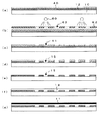
(液晶光変調素子の基本構成、図1参照。)
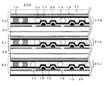
図1(a)〜(d)に液晶表示素子の一例の断面図を示す。以下、図1(a)を例にとって液晶光変調素子の基本構成について説明する。図1(a)に示すように、2枚の透明電極11付き透明基板10の間に、液晶材料25と基板間ギャップ制御用のスペーサ20が配置されており、周辺部には液晶注入口を除いて連続したシール19が配置されている。なお、図1では、基板の一端部のみを図示している。素子の背面側には光吸収層30が設けられている。
【0049】
透明基板としては、ガラス基板や、ポリカーボネート、ポリエーテルスルホン(PES)、ポリエチレンテレフタレート等のフレキシブルな樹脂基板等が使用可能である。なお、液晶光変調素子を反射型素子や光書き込み型素子に用いる場合は一方の基板は透明である必要はない。
【0050】
透明基板10上に設ける液晶光変調素子制御用の透明電極11としては、ITOに代表される透明導電膜、アルミニウムやシリコン等の金属電極、あるいはアモルファスシリコンやBSO等の光導電性膜などが用いられる。複数の画素電極とそれに接続する薄膜トランジスタを形成したアクティブマトリクス型の電極構造も使用可能である。電極材自身を基板として用いることも可能である。
【0051】
基板10の電極形成面には、必要に応じてポリイミドに代表される配向膜を配したり、ガスバリア層や絶縁層として任意の有機系、無機系の膜を配して液晶光変調素子の信頼性を向上させるようにしてもよい。図1では、両基板ともに絶縁膜18と配向膜11とを設けた例を示している。
【0052】
スペーサ20としては、ガラス製、プラスチック製等の球状の粒子を用いることができる。
【0053】
シール19としては、液晶組成物を液晶表示素子内部に封入できるものであれば特に制限はないが、紫外線硬化樹脂や熱硬化性樹脂等を用いることが好ましい。特に、シール樹脂としてエポキシ樹脂材料などの熱硬化性樹脂材料を用いると、長期にわたり高い気密性を保つことができる。
【0054】
各基板10に設けられた電極12間に電圧を印加することにより、液晶をプレーナ状態からフォーカルコニック状態へ、また、フォーカルコニック状態からプレーナ状態に切り変えることができる。
【0055】
液晶材料25としては、光変調にフォーカルコニック相を利用するモードに利用できるものであり、コレステリック液晶や、ネマチック液晶にカイラル剤を添加して室温でコレステリック相を示すように調製されたカイラルネマチック液晶が使用できる。いずれも誘電異方性が正である液晶材料を用いることができる。
【0056】
なお、フォーカルコニック状態とは、液晶の螺旋軸が上下両方の基板面に対して平行になるように液晶分子が並列に配列した状態を指す。ただし、通常、この場合の螺旋軸の方位は一定でない。
【0057】
液晶材料を一対の基板間に狭持する方法としては、一般によく知られた真空注入法や液晶滴下法が利用可能であり、作製する液晶素子のサイズ、基板間ギャップ等を考慮して適宜選択することができる。
【0058】
図7に示すように、上下基板10に対して平面的に接触する(好ましくは上下基板に接着する)構造体28が設けられていてもよい。このような構造体を設けることにより、基板間ギャップの精度が向上する。特に、上下基板を接着しているときは、基板間隔が広がるのを防止でき、樹脂製フィルム基板を用いたときに有効である。構造体28としては、各種の樹脂材料を用いることができる。
【0059】
図1(a)における突起状構造物、図1(b)における絶縁膜に形成された溝、図1(c)における透明電極に形成された溝、図1(d)における配向規制力の異なる部位が、それぞれフォーカルコニック状態における液晶の螺旋軸を規制する領域(以下、配列規制領域と呼ぶ)に相当している。以下、この点について詳述する。
【0060】
なお、螺旋軸の方向を規則的に配置させる効果については、液晶の狭持方法や、スペーサ20の種類、構造体28の有無等によって、液晶分子の螺旋軸の方向には大きな影響は見られないことが確認されている。
(螺旋軸方向の規制方法、図2〜図6参照。)
(1)電界の制御による方法
螺旋軸の方向を基板と平行な面内において規則的に配列させる一つの方法としては、電界の制御による方法が挙げられる。以下、電界の制御による方法について説明する。
【0061】
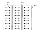
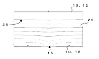
例えば、図1(a)に示すような、リブ状の突起状構造物13を一方の基板10に設けている場合、突起状構造物13を設けたことにより、電極12間に電圧印加した場合に、図2に示すように等電位線26が突起状構造物13近傍で歪を生じる。そのため、図3に示すように電界方向27が部分的に特定方向に傾斜する。そして、この状態から電圧の印加を停止して液晶をフォーカルコニック状態にすると、それまで存在していた傾斜電界の影響により、液晶の螺旋軸方向が規制されるものと考えられ、結果的に図4及び図5に示すように、基板に略平行な面内において、液晶の螺旋軸22が規則的に揃った状態となる。従って、液晶分子の螺旋軸22が一定の方向に向いた光散乱の少ないフォーカルコニック状態を実現することができる。
【0062】
また、図1(b)に示すように、絶縁膜18に溝14を設けた場合も同様に電界方向が傾斜するので、液晶の螺旋軸が一定の方向に向いた光散乱の少ないフォーカルコニック状態を実現することができる。
【0063】
図1(c)に示すように、透明電極12に溝15を形成した場合にも、やはり図6に示すように溝15近傍で等電位線26に歪みを生じるため、同様の理由で液晶の螺旋軸が一定の方向に向いた光散乱の少ないフォーカルコニック状態を実現することができる。
(1−a)突起状構造物
突起状構造物を構成する材料としては、フォトリソグラフィー法により作製する場合には、ノボラック系樹脂に代表されるポジ型フォトレジスト、アクリル系樹脂に代表されるネガ型フォトレジストが使用可能である。また、印刷法により作製する場合には、エポキシ系樹脂に代表される熱硬化性樹脂、ポリウレタン樹脂、ポリ塩化ビニル樹脂に代表される熱可塑性樹脂材料や、ガラスペーストを既存の印刷法にて基板上に形成することも可能である。
【0064】
液晶層挟持用の基板として、樹脂製フィルム基板を用いる場合には、基板そのものに凹凸を形成した後、フィルム基板上に電極を形成することにより、突起状構造物付き基板が容易に得られる。フィルム基板そのものに凹凸を設ける方法としては、押し型を押し当てて凹凸を形成する方法(モールド法)を用いることができる。
【0065】
突起状構造物を設けることによって、螺旋軸の方向を基板と平行な面内において規則的に配列させる方法は、液晶分子への規制力を大きくしやすいという利点がある。
【0066】
このような螺旋軸に規制力を及ぼす突起状構造物は、透明電極上に形成されていることが望ましい。突起状構造物はその高さについても螺旋軸の方向づけには重要なパラメータとなり、望ましい高さの範囲は基板間ギャップをd、突起状構造物の高さをhとした場合はd/20<h<d/2の範囲である。突起状構造物の高さhが上記範囲よりも大きい場合には実効的な基板間ギャップが低下し、コレステリック液晶表示素子として観察した場合、プレーナ状態での表示明るさが低下するという問題がある。一方、突起状構造物の高さhが低い場合には、規制力が低下し螺旋軸を一方向に方向づけるという効果がなくなってしまう。
【0067】
突起状構造物の高さはスピンコート回転数や版の厚みを変更することで任意に調整できる。
【0068】
上記突起状構造物に関してはその形状も重要であり、図5に示すような滑らかな等電位曲線26を得るためには、その側面形状が基板法線方向に対して傾きを有することが望ましい。
【0069】
基板上に形成した突起状構造物に対して基板法線方向に傾斜を設けるには、例えば、突起状構造物を形成した後に熱処理を加えて断面を溶融することにより傾斜を形成する方法を用いることができる。
【0070】
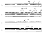
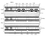
図8は突起状構造物の形成例を示している。本例は以下の各工程からなる。
・図8(a):電極12がパターン形成された基板10の電極面に、レジスト膜40を形成する。
・図8(b):マスク62の開口部63を介してレジスト膜40を露光する。
・図8(c):現像およびリンスによってレジスト膜40の不要部分を除去し、突起状樹脂構造物13を形成する。
・図8(d):加熱処理等により、突起状構造物13に傾斜を持たせる。
・図8(e):基板10の突起状構造物13形成面に絶縁膜18を形成する。
・図8(f):絶縁膜18の上に配向膜11を形成する。
【0071】
以上の工程により、比較的簡単な手法で、所望の形状を有した突起状構造物13を任意の位置に形成することができる。
(1−b)電極の溝
電極に溝を設けるには、既存のフォトリソグラフィー工程を採用すればよい。フォトリソグラフィー法を用いることにより、簡便に溝を形成することができ、画素電極形成時に同時に溝を形成することにより工程の簡略化につながる。溝を一方の基板のみに設けてもよいし、両方の基板に設けてもよい。
【0072】
電極に溝を設けることによって、螺旋軸の方向を基板と平行な面内において規則的に配列させる方法は、電極のパターニングと同時に溝を形成できるため製造工程が簡易になり、不純物や塵などが混入する恐れが低く、また、液晶素子中に新たな部材を追加しないため信頼性が高まるという利点がある。
【0073】
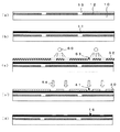
図9は、電極への溝の形成例を示している。本例は以下の各工程からなる。
・図9(a):基板10上に電極層12を形成し、さらにその上にレジスト膜40を形成する。
・図9(b):マスク62の開口部63を介してレジスト膜40を露光する。
・図9(c):現像およびリンスによってレジスト膜40の不要部分を除去し、レジスト膜40に開口41を設ける。
・図9(d):電極層12のエッチングを行うことにより、電極層12を帯状にパターニングするとともに、溝14を形成する。
・図9(e):レジスト膜40を除去する。
・図9(f):基板10の電極面に絶縁膜18を形成する。
・図9(g):絶縁膜18上に配向膜11を形成する。
【0074】
以上の工程により、比較的簡単な手法で、所望の形状を有した溝14を任意の位置に形成することができる。
(1−c)絶縁膜の溝
絶縁膜に溝を設けるには、例えば、感光性の樹脂材料を絶縁膜の材料として用いるフォトリソグラフィー法を用いることができる。また、このような樹脂材料としては、液晶材料との誘電率差が大きいものほど効果的であり、使用する液晶材料に合せて適宜選択すればよい。絶縁膜に設ける溝は一方の基板のみであってもよいし、両方の基板であってもよい。
【0075】
絶縁膜に溝を設けることによって、螺旋軸の方向を基板と平行な面内において規則的に配列させる方法は、液晶素子中に新たな部材を追加しないため信頼性が高まるという利点がある。
【0076】
図10は、絶縁膜に溝を形成する工程の一例を示している。本例は以下の各工程からなる。
・図10(a):電極12のパターン形成された基板10の電極面にレジスト膜42形成する。
・図10(b):マスク62の開口部63を介してレジスト膜42を露光する。・図10(c):現像およびリンスによってレジスト膜42の不要部分を除去し、レジスト膜42に開口を設ける。レジスト膜42を硬化処理することにより、絶縁膜18とする。こうして、前記開口が絶縁膜18の溝14となる
・図10(d):絶縁膜18の形成面に配向膜11を形成する。
【0077】
以上の工程により、比較的簡単な手法で、所望の形状を有した溝14を任意の位置に形成することができる。
(2)配向規制力を異ならせることによる方法
螺旋軸の方向を基板と平行な面内において規則的に配列させる他の方法としては、配向規制力の異なる部分を設ける方法が挙げられる。配向規制力の異なる部分とは液晶分子に対するアンカリング力や配向方向が異なる部分を指し、電極面に均一に塗布されたポリイミド等の配向膜を部分的にラビング処理したり紫外線等による光配向処理を施すことにより得られる。また、部分的に材料種の異なる配向膜を形成することによっても配向規制力の異なる部分が得られる。図1(d)は配向規制力の異なる部分16を配向膜11上に設けた例を示している。
【0078】
このような配向規制力の異なる部分を設ける方法においては、ラビング処理等により電界方向の傾斜が発現するのではなく、液晶分子がフォーカルコニック状態に遷移する過程において、表面規制力の違いによる螺旋軸の方向付けがなされるため、上記の電界方向を傾斜させる方法と同様の効果を得ることができるものと考えられる。
【0079】
配向膜を部分的にラビングする方法としては、形成した配向膜にフォトレジスト材料をスピンコート等により塗布し、既存のフォトリソグラフィー工程によりラビングを行いたい部分のみレジストを除去し、ラビングを行った後、レジストを除去することにより得られる。なお、ラビング方向は特に問わない。
【0080】
光配向の場合はフォトマスク及び偏光板を介して紫外線露光することにより容易に部分的に配向規制力の異なる部分が得られる。
【0081】
図11は、配向膜に配向規制力の異なる領域を形成する工程の一例を示している。本例は以下の各工程からなる。
・図11(a):電極12のパターン形成された基板10の電極面に絶縁膜18を形成する。
・図11(b):絶縁膜18上に配向膜11を形成する。
・図11(c):マスク62の開口部63を介して配向膜11を露光する。
【0082】
または、
・図11(c’):配向膜18上にレジスト膜40を形成し、レジスト膜40をパターニングする。そして、レジスト膜40の開口部41を介して配向膜11をラビング処理64する。その後、レジスト膜40を除去する。
・図11(d):以上により、配向規制力の異なる領域16が形成される。
【0083】
以上の工程により、比較的簡単な手法で、所望の形状を有した配向規制力の異なる領域16を任意の位置に形成することができる。
【0084】
なお、異種配向膜を使用する方法としては、例えば、図11(C)の工程において、レジスト膜のパターニング後、異なる種類の配向膜を塗布し焼成してレジスト膜を除去する方法が採用できる。
【0085】
いずれにしても、配向処理を施すことによって、螺旋軸の方向を基板と平行な面内において規則的に配列させる方法は、液晶素子中に新たな部材を追加する必要がないため信頼性が高まるという利点がある。特に、光配向処理は塵の発生等の恐れが少なく優れた方法である。
(3)配列規制領域の配列(図12参照。)
上記各方法による螺旋軸を一定方向に方向づける規制力の及ぶ範囲については限界があるので、その幅Wが、液晶の螺旋ピッチをpとしたとき、p<W<20pの範囲にあることが望ましい。また、配列規制領域の配列ピッチLは、液晶の螺旋ピッチをpとしたとき、5p<L<100pの関係にあることが好ましい。これらの範囲よりも広くなった場合には規制力の及ばない領域が存在しやすくなり、フォーカルコニック状態におけるドメイン間の散乱が増す。一方、上記範囲よりも小さい場合には開口率の低下の問題や素子製造工程の複雑化の問題が生じる。
【0086】
また、特に配列ピッチが細かくなった場合に、配列ピッチが一様であると突起状構造物による光回折現象が生じ、表示素子として観察した場合に回折光による視認性の低下が生じる。このような現象を回避するためには、配列ピッチを液晶素子内で適当に変化させる(例えば、ランダムピッチとする)ことが有効である。
【0087】
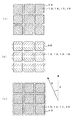
これらの配列規制領域は素子内において一方向のみの形状(直線状)を有するものであってもよいが、セル内で方向が変化する、例えば、図12(a)に示すような“く”の字形状などの屈曲部を有する形状にすることにより、光入射方向に依存することのない一様な光透過特性が得られることとなる。図12(b)のように、規制力を付与する部位を周期的に向きを変えて配置するようにしてもよい。
【0088】
一般に、液晶表示素子を作製する場合にマトリクス画素(縦、横に規則正しく整列した画素群)を形成するが、図12(c)に示すように、上記規制力を付与する構造物の配列方向bは、直線状もしくは“く”の字状を選択した場合でも、画素配列方向aとは異なる方が望ましい。
【0089】
なお、配列規制領域、すなわち、突起状構造物、電極の溝、絶縁膜の溝、配向規制力の異なる領域等の配列ピッチや形状は、マスクや版の形状を変更することにより任意に変更できる。また、配向規制発現領域は一方の基板のみに設けてもよいし、両方の基板に設けてもよい。
(積層型液晶素子、図13〜図16参照。)
フォーカルコニック状態における液晶分子の螺旋軸の方向を規則的にすることによる光散乱の低減の効果は、単層の素子だけでなく、複数の素子を積層した積層型素子にも発現する。積層型素子の場合、通常、1層目に入射した光が1層目の液晶層で散乱し、2層目には直進成分と散乱成分が入射することになりさらに散乱成分が増加してしまう。従って、少なくとも最も観察側の第1番目の素子に液晶の螺旋軸の方向を規則的にするための配列規制領域を形成することにより、効果的に積層型素子の特性向上につなげることができる。
(1)フルカラー用素子(図13、図14参照。)
このような積層型素子として、室温でコレステリック相を示し且つ誘電異方性が正である液晶組成物を用い、かつ各素子の選択反射波長を赤色、緑色、青色に調整した液晶材料を用いることにより、反射型フルカラー液晶表示素子が実現できる。
【0090】
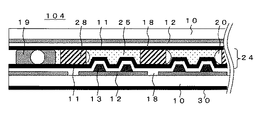
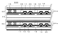
図13に示す積層型素子200は、観察側から順に青色表示用液晶素子50、緑色表示用液晶素子51、赤色表示用液晶素子52を積層し、最背面に光吸収層30を設けている。各素子の基本構成は図1(a)に示したものと同様であるが、各素子の液晶層に含まれる液晶組成物の選択反射波長が異なっており、素子50においては青色領域に選択反射のピーク波長を有する液晶組成物24aが用いられ、素子51においては緑色領域に選択反射のピーク波長を有する液晶組成物24bが用いられ、素子52においては赤色領域に選択反射のピーク波長を有する液晶組成物24cが用いられている。各素子毎にスペーサの径が最適化されていてもよい。
【0091】
各素子の積層順は特に問わないが、コレステリック液晶の選択反射特性を考慮し、観察側から順に青色用素子、緑色用素子、赤色用素子とすることによりプレーナ状態の明るさや色純度等の表示特性が向上する。
【0092】
各素子は接着層23によって貼り合される。貼り合せは、例えば、各素子間に接着剤を滴下し各素子での画素の位置ずれがないようにアライメントをし、各素子を接着することによって行う。この場合、接着剤としては、熱硬化性樹脂材料や光硬化性樹脂材料などの硬化性樹脂材料、あるいは、熱可塑性樹脂などを用いることができる。各素子を粘着剤や粘着シートで貼り合せるようにしてもよい。なお、各液晶層間の基板は兼用されていてもよい。
【0093】
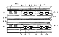
図13に示す積層型素子200では、フォーカルコニック状態の光散乱を低減させるための規制手段である突起状構造物13は、各素子毎に設けている。特に、各素子毎に配列ピッチ、高さ、材料を最適化したものを用いることにより表示特性をさらに向上することができる。図14に示す積層型素子201に示すように、突起状構造物13を観察側の素子50のみに設けてもよい。
【0094】
透明電極に形成する溝、絶縁膜に形成する溝、及び配向膜上の配向規制力の異なる領域に関しても、全ての素子にこれらを設けたり、一部の素子(特に、観察側の素子)のみにこれらを設けてもよい。
(2)高反射率素子(図15、図16参照。)
図15に示す積層型素子300のは、互いに旋光方向の異なる液晶組成物24d、24eをそれぞれ含む2つの液晶素子53、54を積層したものである。一般に、コレステリック液晶がプレーナ状態にあるとき、液晶分子の螺旋軸に平行な方向から入射した光は右旋光と左旋光の2つの円偏光に分かれ、一方は液晶層を透過し、他方は液晶分子によって反射される。よって、素子300のように、互いに旋光方向の異なる複数の素子を積層することにより、光の利用効率を高めることができ、例えば、素子53、54の螺旋ピッチをほぼ同一にした場合、片側旋光のみの素子に比べて約2倍の反射率を得ることができる。
【0095】
また、図16の積層型素子301に示すように、1/2波長板29を間に介して同じ液晶素子53を積層することにより、積層型素子300と同様に光の利用効率を高めることができ、反射率の高い明るい素子が得られる。
【0096】
いずれにしても、少なくとも一つの液晶素子に、フォーカルコニック状態での液晶分子の螺旋軸の方向を基板面と略平行な面内で規則的に配列させるための配列規制手段を備えることによって、極めてコントラストの高い積層型素子を得ることができる。
【0097】
以上、各種の実施形態について説明したが、本発明は上記各実施形態のみに限定されるものではなく、種々の変形が可能である。配向規制手段についても種々の方法を採用することができる。
【0098】
【実験例】
以下、本発明の実験例について説明する。もちろん、材料種や数値等はあくまでも一例であって、本発明がこの実験例に限られるものではない。
<実験例1>
本実験例では、突起状構造物を設ける構成例を示す。
【0099】
ITO付ガラス基板(セントラルガラス社製)を2枚使用し、各基板のITOをフォトリソ法によって帯状にパターニングした(電極幅300μm、ピッチ350μm)。次に、以下の手順で一方の基板のITO形成面に突起状構造物を形成した。
【0100】
まず、2000rpm、30秒の条件でポジ型レジスト(JSR社製PC403)を基板のITO形成面にスピンコートした。そして、クリーンオーブンを用いて90℃で2分間プリベイクした。
【0101】
次に、帯状の開口部(幅4μm)がピッチ10μmで形成されたフォトマスクを使用し、紫外線露光装置を用いて100mJ/cm2の条件で紫外線を照射した。そして、現像液(JSR社製PD‐523ADの0.2%希釈液)で90sec現像し、超純水流水によるリンスを行って不要部を除去し、高さ1.5μmの帯状の構造物を形成した。
【0102】
その後、この構造物を紫外線露光装置によってポスト露光した(300mJ/cm2)。そして、吸着ホットプレートを用いて150℃で5分間ポストベイクし、上記構造物に傾斜部を形成した。最後に、クリーンオーブンを用いて、150℃で120分間本硬化処理を行い、断面が台形状の突起状構造物を形成した。突起状構造物は、高さが約1.5μm、上面の幅が約4μm、下面の幅が約8μm、両斜面部の幅がそれぞれ約2μmであった。
【0103】
次に、突起状構造物の形成された基板面およびもう一方の基板のITO形成面に、それぞれポリシラザン溶液L120(東燃社製)を用い、スピンコート法により両基板の電極面に厚さ1000Åの薄膜を形成し、120℃の恒温槽中で2時間加熱し、さらに、90℃、湿度85%の恒温恒湿槽中で3時間加熱することにより絶縁膜を形成した。そして、フレキソ印刷によってポリイミド材料(JSR社製AL‐8044)を塗布し、80℃で2分間仮焼成した。さらに、160℃で60分間焼成することにより配向膜を形成した。
【0104】
そして、突起状構造物の形成された基板上に5μmのスペーサ(積水化学社製ミクロパールSP2050μm)を散布し、他方の基板に液晶注入口を残してシール剤(三井化学社製XN21S)を形成した上で両基板を貼り合せ、空セルを作製した。
【0105】
液晶組成物としては、メルク社製ネマティック液晶E−31LVに、メルク社製カイラル剤S−811を24.5wt%添加して、選択反射のピーク波長がλ=550nmに調整されたカイラルネマティック液晶を用いた。液晶組成物の螺旋ピッチは約343nmであった。そして、この液晶組成物を真空注入法によりセルに注入した。最後に液晶注入口を封止剤で封止して液晶光変調素子とした。
【0106】
こうして得られた液晶光変調素子の上下基板の透明電極間に電圧を印加してフォーカルコニック状態にした後、素子の特性評価を行った。評価は分光光度計(日立)を用い、積分球から離して透過率を測定することによって行った。
【0107】
その結果、素子の透過率は78%となった。比較のため突起状構造物を設けない以外は上記と同じ手順で素子を作製したところ、透過率は62%であった。突起状構造物の有無によるドメインの様子の違いを確認するため、フォーカルコニック状態にした素子の偏光顕微鏡観察を行ったところ、突起状構造物を設けた本実験例の素子では、液晶の螺旋軸の方向が規制され、螺旋軸が揃った状態であることが観察された。これに対して、突起状構造物を設けていない比較用素子では、各ドメインの螺旋軸がランダムになるように各ドメインが配列しているのが観察された。
【0108】
突起状構造物の高さ、幅、配列ピッチを種々変更してその影響を調べたところ、これらの値が大きすぎたり小さすぎて、先に説明した範囲を越える透過率が低下する傾向が見られた。
【0109】
また、突起状構造物の配列ピッチを一様なものとランダムなものとに変化させてその影響を調べたところ、透過率は同等の値を示したが、配列ピッチが一様なものでは、特定の角度で回折光が観察され、視認性が低下しやすくなる傾向が見られた。
【0110】
さらに、突起状構造物の配列方向と画素配列方向とを種々変更してその影響を調べたところ、透過率はいずれも同等の値を示したが、両者の方向が揃っている場合は、モアレにより表示品位が悪化しやすくなる傾向が見られた。
【0111】
さらにまた、突起状構造物の長手方向の形状を直線状のものとくの字状にしたものとに変化させてその影響を調べたところ、いずれの場合も透過率は同等であったが、突起状構造物の形状が直線状である場合は、突起状構造物の配列方向と同一方向から観察した場合と垂直方向から観察した場合とで視認性が異なりやすくなる傾向が見られた。
<実験例2>
本実験例では、透明電極に溝を設ける構成例を示す。
【0112】
ITO付ガラス基板(セントラルガラス社製)を2枚使用し、各基板のITOをフォトリソ法によって帯状にパターニングした(電極幅300μm、ピッチ350μm)。この際、一方の基板には、以下の手順でITOをパターニングすると同時に溝も形成した。
【0113】
まず、基板のITO形成面にポジ型レジスト(東京応化社製OFPR−800)をスピンコートし、クリーンオーブンを用いて、80℃で15分間プリベイクした。その後、帯状の開口部(幅4μm)がピッチ10μmで形成された領域が300μm、遮光部が幅50μmで交互に形成されたフォトマスクを介して紫外線露光装置により30mJ/cm2で露光を行った。
【0114】
次に、現像液(トクヤマ社製SD‐1)を用いて現像を行い、超純水流水によってリンスすることにより不要部を除去し、120℃で15分間ポストベイクした。その後、塩鉄液D(林純薬社製)を用いて20分間ITOのエッチング処理を行った。最後に、NaOHの2%水溶液を用いて、2分間レジスト剥離処理を行った。こうして、一方の基板上に溝の形成されたITOパターンを形成した。
【0115】
その後、実験例1と同様の手順で、絶縁膜及び配向膜の形成、スペーサ散布、シール剤形成、基板貼り合せ、液晶注入を行い、液晶光変調素子を作製した。
【0116】
得られた液晶光変調素子に電圧を印加しフォーカルコニック状態にした後、実験例1と同様の手順で評価を行った。その結果、透過率は82%となった。
【0117】
溝の幅や配列ピッチを種々変更してその影響を調べたところ、これらの値が大きすぎたり小さすぎて先に説明した範囲を越えると透過率が低下する傾向が見られた。
【0118】
また、溝の配列ピッチを一様なものとランダムなものとに変化させてその影響を調べたところ、透過率は同等の値を示したが、配列ピッチが一様なものでは、特定の角度で回折光が観察され、視認性が低下しやすくなる傾向が見られた。
【0119】
さらに、溝の配列方向と画素配列方向とを種々変更してその影響を調べたところ、透過率はいずれも同等の値を示したが、両者の方向が揃っている場合は、モアレにより表示品位が悪化しやすくなる傾向が見られた。
【0120】
溝の長手方向の形状を直線状のものとくの字状にしたものとに変化させてその影響を調べたところ、いずれの場合も透過率は同等であったが、溝の形状が直線状である場合は、溝の配列方向と同一方向から観察した場合と垂直方向から観察した場合とで視認性が異なりやすくなる傾向が見られた。
<実験例3>
本実験例では、配向膜にラビング処理を施す構成例を示す。
【0121】
ITO付ガラス基板(セントラルガラス社製)を2枚使用し、各基板のITOをフォトリソ法によって帯状にパターニングした(電極幅300μm、ピッチ350μm)。
【0122】
次に、両基板のITO形成面に、それぞれ絶縁性材料を塗布し焼成することにより絶縁膜を形成した。そして、フレキソ印刷によってポリイミド材料(JSR社製AL‐8044)を塗布し、80℃で2分間仮焼成した。さらに、160℃で60分間、焼成することにより配向膜を形成した。
【0123】
次に、一方の基板の配向膜形成面にポジ型レジスト(東京応化社製OFPR−800)を配向膜上にスピンコートし、クリーンオーブンを用いて、80℃で15分間プリベイクした。
【0124】
そして、実験例1で用いたのと同様の開口部を有したフォトマスクを用いて、紫外線露光装置を用いて、30mJ/cm2露光した。次に、現像液(トクヤマ社製SD‐1)を用いて現像し、超純水流水を用いてリンスすることにより不要部分を除去した。その後、120℃で15分間ポストベイクした。こうして、次のラビング処理に対するマスク層を形成した。
【0125】
次に、マスク層の形成された基板に対してラビング処理を行った。ラビング処理は、毛先押し込み長さ0.4mm、ロール半径75mmの植毛ロールを用いて、ロール回転数900rpm、基板移動速度30mm/秒の条件で、マスク層の上から2回ラビングすることで行った。
【0126】
ラビング処理後、イソプロピルアルコール(IPA)を用いて2分間レジスト剥離を行ってマスク層を除去した。そして、実験例1と同様の手順で、スペーサ散布、シール剤形成、基板貼り合せ、液晶注入を行い、液晶光変調素子を作製した。
【0127】
得られた液晶光変調素子に電圧を印加しフォーカルコニック状態にた後、実験例1と同様にして測定を行ったところ、透過率は約80%であった。
【0128】
ラビング処理部の幅や配列ピッチを種々変更してその影響を調べたところ、これらの値が大きすぎたり小さすぎて先に説明した範囲を越えると透過率が低下する傾向が見られた。
【0129】
また、ラビング処理部の配列ピッチを一様なものとランダムなものとに変化させてその影響を調べたところ、透過率は同等の値を示したが、配列ピッチが一様なものでは、特定の角度で回折光が観察され、視認性が低下しやすくなる傾向が見られた。
【0130】
さらに、ラビング処理部の配列方向と画素配列方向とを種々変更してその影響を調べたところ、透過率はいずれも同等の値を示したが、両者の方向が揃っている場合は、モアレにより表示品位が悪化しやすくなる傾向が見られた。
【0131】
ラビング処理部の形状を直線状のものとくの字状にしたものとに変化させてその影響を調べたところ、いずれの場合も透過率は同等であったが、ラビング処理部の形状が直線状である場合は、ラビング処理部の配列方向と同一方向から観察した場合と垂直方向から観察した場合とで視認性が異なりやすくなる傾向が見られた。
<実験例4>
本実験例では、配向膜に光配向処理を施す構成例を示す。
【0132】
ITO付ガラス基板(セントラルガラス社製)を2枚使用し、各基板のITOをフォトリソ法によって帯状にパターニングした(電極幅300μm、ピッチ350μm)。
【0133】
次に、両基板のITO形成面に、それぞれポリシラザン溶液L120(東燃社製)を用い、スピンコート法により両基板の電極面に厚さ1000Åの薄膜を形成し、120℃の恒温槽中で2時間加熱し、さらに、90℃、湿度85%の恒温恒湿槽中で3時間加熱することにより絶縁膜を形成した。そして、ポリイミド材料(日立化成社製TT−054)を、3000rpm、30秒間の条件でスピンコートし、100℃で1分間仮焼成した。さらに、230℃で30分間焼成することにより、配向膜を形成した。
【0134】
そして、一方の基板の配向膜に対して、実験例1と同様の開口部が形成されたフォトマスクと偏光板とを介して、紫外線照射装置により5J/cm2で照射角度15度として光照射を行い、部分的に光配向処理を行った。
【0135】
その後、実験例1と同様の手順で、スペーサ散布、シール剤形成、基板貼り合せ、液晶注入を行い、液晶光変調素子を作製した。
【0136】
得られた液晶光変調素子に電圧を印加しフォーカルコニック状態にした後、実験例1と同様にして測定を行ったところ、透過率は約80%であった。
【0137】
光配向処理部の幅や配列ピッチが大きすぎたり小さすぎて先に説明した範囲を越えると透過率が低下する傾向にある点、光配向処理部の配列ピッチを素子内で一様とすると透過率は同等であるが回折光による影響で視認性が低下しやすくなる傾向にある点、光配向処理部の配列方向を画素配列方向と同一とした場合に透過率は同等であるが、モアレの影響で表示品位が悪化しやすくなる傾向にある点、光配向処理部の配列を一直線とした場合に透過率は同等であるが、配列と同一方向から観察した場合と垂直方向から観察した場合とで視認性が異なりやすくなる点は、実験例3と同様であった。
<実験例5>
本実験例では、絶縁膜に溝を形成する構成例を示す。
【0138】
ITO付ガラス基板(セントラルガラス社製)を2枚使用し、各基板のITOをフォトリソ法によって帯状にパターニングした(電極幅300μm、ピッチ350μm)。
次に、一方の基板のITO形成面に、ポジ型レジスト(JSR社製PC335)を、3000rpm、30秒間の条件でスピンコートし、クリーンオーブンを用い、90℃で2分間プリベイクした。その後、幅2μm、配列ピッチ10μmの開口部が形成されたフォトマスクを介して、紫外線露光装置により100mJ/cm2露光を行った。
【0139】
そして、現像液(JSR社製PD−523AD)の5倍希釈液を用いて、90秒間現像し、超純粋流水を用いてリンスすることにより不要部分を除去した。次に、紫外線露光装置を用いて300mJ/cm2ポスト露光を行った。最後に、クリーンオーブンを用いて、150℃で120分間本硬化を行って帯状の溝を有する高さ0.5μmの絶縁膜を形成した。
【0140】
その後、実験例1と同様の手順で、配向膜の形成、スペーサ散布、シール形成、基板貼り合せ、液晶注入の各工程を経て、液晶光変調素子を作製した。
【0141】
得られた液晶光変調素子の電極間に電圧を印加しフォーカルコニック状態にした後、実験例1と同様にして測定を行ったところ、透過率は約80%であった。
【0142】
溝の幅や配列ピッチを種々変更してその影響を調べたところ、これらの値が大きすぎたり小さすぎて先に説明した範囲を越えると透過率が低下する傾向が見られた。
【0143】
また、溝の配列ピッチを一様なものとランダムなものとに変化させてその影響を調べたところ、透過率は同等の値を示したが、配列ピッチが一様なものでは、特定の角度で回折光が観察され、視認性が低下しやすくなる傾向が見られた。
【0144】
さらに、溝の配列方向を溝の配列方向と画素配列方向とを種々変更してその影響を調べたところ、透過率はいずれも同等の値を示したが、両者の方向が揃っている場合は、モアレにより表示品位が悪化しやすくなる傾向が見られた。画素配列方向と同一とした場合も透過率は同等であったが、モアレにより表示品位がやや悪化した。
【0145】
さらにまた、溝の長手方向の形状を直線状のものとくの字状にしたものとに変化させてその影響を調べたところ、いずれの場合も透過率は同等であったが、溝の形状が直線状である場合は、溝の配列方向と同一方向から観察した場合と垂直方向から観察した場合とで視認性が異なりやすくなる傾向が見られた。
<実験例6>
本実験例では、積層型液晶素子において、突起状構造物を設ける構成例を示す。
【0146】
基板として、可撓性を有するITO付きフィルムFST−5352(住友ベークライト社製)を2枚用いた。これらの基板上のITOをフォトリソグラフィ工程により、電極ピッチ350μm、電極幅300μmでパターニングし、帯状の透明電極を形成した。 次に、一方の基板(第1基板とする)の透明電極形成面に、ピッチ10μm、高さ1.5μm、頭頂部幅4μm、傾斜部幅2μmの断面台形状の突起状構造物を、実験例1と同様にして形成した。
【0147】
そして、ポリシラザン溶液L120(東燃社製)を用い、スピンコート法により両基板の透明電極形成面に、厚さ1000Åの薄膜を形成し、120℃の恒温槽中で2時間加熱し、さらに、90℃、湿度85%の恒温恒湿槽中で3時間加熱することにより、絶縁膜を形成した。次に、配向膜材料AL4552(JSR社製)を用いて、スピンコート法で両基板の絶縁膜上に厚み500Åの薄膜を形成し、165℃で2時間恒温槽中で加熱し、配向膜を形成した。なお、配向膜のラビング処理は行わないようにした。
【0148】
次に、第1基板の周辺部に、スペーサとして粒径が5μmのミクロパールSP−205を混入した紫外線硬化型樹脂(エポキシ樹脂)材料のUV RESINT−470/UR−7092(長瀬チバ社製:ガラス転移点144℃)を、スクリーン印刷法により塗布した後、4kWの高圧水銀灯HMW−244−11CM(オーク社製)により、積算光量で4000mJ/cm2照射して、シールを形成した。このとき、シールは表示領域を囲む環状構造とした。シールとなる樹脂材料を描画後、第1基板に対しては、真空吸着可能なホットプレート上で吸着固定して80℃で30分間加熱した。
【0149】
次に、突起状構造物を設けていない方の基板(第2基板とする)上に、第1及び第2基板を接着するための樹脂構造物を形成した。ここでは、熱可塑性樹脂であるポリエステル樹脂(スリーボンド社製アロンメルトPES−360SA40)を用いて、スクリーン印刷法により、直径50μm、ピッチ350μm、高さ6.5μmで格子状に樹脂構造物を配置した。
【0150】
こうして、貼り合わせ前の2枚の基板を作製し、ホットプレート上に第1基板を真空吸着し、予め所望の粒径のスペーサを分散させた液晶組成物を基板上の端部に塗布した。次に、第2基板を、液晶組成物を塗布した側の端部で両基板を互いの帯状電極が直交するように重ね合わせ、加熱ローラ及び加圧ローラによって押圧することにより貼り合わせた。
【0151】
貼り合わせに際して、第1基板に関しては配向膜が形成されている面を上にして80℃に予め加熱されているホットプレート上に真空吸着して固定し、第1基板の端部に液晶組成物を滴下した。滴下量はにシールと両基板とで囲まれた体積以上の量を滴下した。
【0152】
液晶組成物は、ネマティック液晶E44にカイラル材S811を(共にメルク社製)32wt%添加したものを用いた。また、液晶組成物には、スペーサとして粒径が5μmのミクロパールSP−205を混合しておいた。こうして、液晶層の選択反射波長が490nmの青色表示用液晶素子を作製した。液晶組成物の螺旋ピッチは約306nmであった。
【0153】
以下同様の手順で、緑色表示用液晶素子及び赤色表示用液晶素子を作製した。液晶組成物としては、ネマティック液晶E44にカイラル材S811(共にメルク社製)を緑色表示用表示素子は30wt%、赤色表示用液晶素子は25wt%を添加したものを用いた。また、スペーサは、基板間ギャップをそれぞれ7μm、9μmとするため、粒径7μmのSP207、粒径9μmのSP209(共に積水ファインケミカル社製)を用いた。緑色表示用液晶素子の選択反射波長は560nm、赤色表示用液晶素子の選択反射波長は680nmであった。液晶組成物の螺旋ピッチはそれぞれ、約350nm、約425nmであった。
【0154】
このようにして、各色表示用の素子を作製した後、各素子の画素を合せて各素子を粘着剤(積水社製WT−#5511)によって貼り合せ、第3層目の基板の透明電極が設けられていない面には光吸収層を設け、積層型液晶素子とした。
【0155】
上記積層型液晶素子の各素子に所定の電圧を印加して、全ての液晶層をフォーカルコニック状態とし、ミノルタ社製分光測色計CM3700dで測定したところ、Y値が3.5となった。突起状構造物が無い場合はY値が4.5であった。<実験例7>
本実験例では、積層型液晶素子において、2つの素子に突起状構造物を設ける構成を示す。
【0156】
青色表示用液晶素子に加えて、緑色表示用液晶素子においても実験例6と同様の手順で、ピッチ14μm、高さ1.5μm、頭頂部幅4μm、傾斜部2μmの突起状構造物を形成した以外は実験例6と同様にして積層型液晶素子を作製した。
【0157】
こうして得られた積層型液晶光変調素子の各素子に所定の電圧を印加して、全ての液晶層をフォーカルコニック状態とし、ミノルタ社製分光測色計CM3700dで測定したところ、Y値が3.1となった。
<実験例8>
本実験例では、積層型液晶素子において、3つの素子に突起状構造物を設ける構成を示す。
【0158】
青色表示用液晶素子及び緑色表示用液晶素子に加えて、赤色用表示素子においても実験例6と同様の手順で、ピッチ18μm、高さ1.5μm、頭頂部幅4μm、傾斜部2μmmの突起状構造物を形成した以外は、実験例6と同様の手順で突起状構造物を作製し、積層型液晶素子を作製した。
【0159】
こうして得られた積層型液晶光変調素子の各素子に所定の電圧を印加して、全ての液晶層をフォーカルコニック状態とし、ミノルタ社製分光測色計CM3700dで測定したところ、Y値が2.8となった。
<実験例9>
本実験例では、積層型液晶素子において、透明電極に溝を設ける構成を示す。
【0160】
緑色表示用液晶素子の観察側とは反対側の基板の透明電極上に、ピッチ10μm、幅3.0μmの溝を形成し、突起状構造物を設けない以外は実験例5と同様の手順で緑色表示用液晶素子を作製した。なお、溝の形成方法は実験例2と同様にした。
【0161】
そして、青色表示用液晶素子及び赤色表示用液晶素子は、実験例5と同様の手順で、突起状構造物も透明電極上の溝も設けることなく作製し、積層型液晶素子を得た。
【0162】
こうして得られた積層型液晶光変調素子の各素子に所定の電圧を印加して、全ての液晶層をフォーカルコニック状態とし、ミノルタ社製分光測色計CM3700dで測定したところ、Y値が3.4となった。
<実験例10>
本実験例では、積層型液晶素子において、3つの素子に突起状構造物を設け、各素子の突起状構造物の大きさ及び配列ピッチを異ならせた構成を示す。
【0163】
突起状構造物を形成する際のフォトマスクを変更して、各素子の突起状構造物の大きさと配列ピッチを異ならせるようにした以外は、実験例7と同様の手順で、積層型液晶素子を作製した。なお、青色表示用液晶素子にはピッチ10μm、幅3.0μmの突起状構造物を、緑色表示用液晶素子にはピッチ14μm、高さ3.5μmの突起状構造物を、赤色表示用液晶素子にはピッチ18μm、高さ4.5μmの突起状構造物をそれぞれ形成した。
【0164】
こうして得られた積層型液晶光変調素子の各素子に所定の電圧を印加して、全ての液晶層をフォーカルコニック状態とし、ミノルタ社製分光測色計CM3700dで測定したところ、Y値が2.8となった。
<実験例11>
本実験例では、同一選択波長で螺旋方向が異なるセルを2層積層した構成を示す。
【0165】
液晶組成物は、左旋性カイラルネマティック液晶材料として、ネマティック液晶E−31LVにカイラル材S−811(いずれもメルク社製)を24.5wt%添加したものを用い、右旋性カイラルネマティック液晶材料として、ネマティック液晶E−31LVにカイラル材R−811(いずれもメルク社製)を24.5wt%添加したものを用いた。いずれも、選択反射波長が550nmの緑色表示用液晶素子である。液晶組成物の螺旋ピッチはいずれも343nmであった。
【0166】
そして、実験例1と同様の製造方法、突起状構造物にて各素子を作製した。作製した素子を透明粘着層を介して積層することにより、反射時の反射率が73%、透過時の反射率が2%の極めてコントラストの高い素子が得られた。
【図面の簡単な説明】
【図1】液晶光変調素子の構成を示す断面図である。
【図2】突起状構造物を設けた場合の等電位曲線を示す図である。
【図3】液晶素子に電圧を印加した場合の電界分布を示す模式図である。
【図4】電圧除去後のフォーカルコニック状態における各液晶ドメインの螺旋軸方向を示す図である。
【図5】配列規制手段を設けた場合の、フォーカルコニック状態における各液晶ドメインの螺旋軸の方向を示す模式図である。
【図6】電極に溝を設けた場合の等電位曲線を示す図である。
【図7】液晶光変調素子の他の構成を示す断面図である。
【図8】液晶光変調素子の製造工程の一例を示す図である。
【図9】液晶光変調素子の製造工程の一例を示す図である。
【図10】液晶光変調素子の製造工程の一例を示す図である。
【図11】液晶光変調素子の製造工程の一例を示す図である。
【図12】他の配列規制手段を設けた実施形態を示すである。
【図13】積層型液晶素子の構成を示す断面図である。
【図14】積層型液晶素子の他の構成を示す断面図である。
【図15】積層型液晶素子の他の構成を示す断面図である。
【図16】積層型液晶素子の他の構成を示す断面図である。
【図17】従来の液晶素子における、フォーカルコニック状態の各液晶ドメインの螺旋軸の方向を示す模式図である。
【符号の説明】
10 基板
11 配向膜
12 電極
13 突起状構造物
14 絶縁膜の溝
15 電極の溝
16 配向膜の配向規制力が異なる領域
18 絶縁層
19 シール
20 スペーサ
22 液晶の螺旋軸方向
23 接着層
24、24a、24b、24c、24d、24e 液晶層
25 液晶組成物
26 等電位線
27 電界の方向
28 樹脂構造物
29 1/2波長板
30 光吸収層
40、42 レジスト膜
41、43 レジスト膜の開口部
45 画素
51、52、53、54 素子
60 光源
62 マスク
63 開口部
64 ラビング処理
100、101、102、103、104 液晶表示素子
200、201、300、301 積層型液晶表示素子[0001]
[Industrial applications]
The present invention relates to a liquid crystal light modulation device and a method for manufacturing the same.
[0002]
[Prior art]
As a typical liquid crystal material used for a liquid crystal display device using a focal conic state of liquid crystal molecules, cholesteric liquid crystal is cited. The cholesteric liquid crystal includes a liquid crystal which itself shows a cholesteric phase and a chiral nematic liquid crystal obtained by adding a chiral agent to a nematic liquid crystal. Cholesteric liquid crystals have the characteristic that liquid crystal molecules form a helical structure. When a liquid crystal molecule is held between a pair of substrates and an external stimulus such as an electric field, magnetic field, or temperature is applied to the liquid crystal, the cholesteric liquid crystal becomes planar. , A focal conic state, and a homeotropic state.
[0003]
Since these three states have different light transmittance and reflectivity, display can be performed by appropriately selecting the three states and an external stimulus applying method. Examples include a cholesteric-nematic phase transition mode using a homeotropic state and a focal conic state, and a bistable mode using a planar state and a focal conic state.
[0004]
Among them, the bistable mode has a feature that the planar state and the focal conic state are stable even when no external stimulus is applied. Therefore, the bistable mode has been actively studied in recent years as a memory display element (display is stable). In particular, a liquid crystal element using a cholesteric liquid crystal having a selective reflection characteristic in a visible region in a planar state has a memory property and can obtain a bright color reflection state, and is therefore expected to be applied to a power saving display element.
[0005]
[Problems to be solved by the invention]
The focal conic state of the cholesteric liquid crystal is a state in which the helical axis of the liquid crystal molecules is oriented in the direction of the substrate plane. Normally, liquid crystals are divided into a plurality of liquid crystal molecular domains. The helical axis of the liquid crystal is the same in the domain, but the
[0006]
In addition, it is known that a reflective liquid crystal element having a memory property can obtain an element capable of full-color display by stacking a plurality of elements having different selective reflection wavelengths. In this case, the influence of the inter-domain scattering is particularly large due to multiple scattering between the elements, and the contrast is likely to be deteriorated.
[0007]
Therefore, an object of the present invention is to provide a liquid crystal light modulation element with low light scattering in the element and high contrast. Another object of the present invention is to provide a liquid crystal light modulation device having a stacked structure with high contrast. Still another object of the present invention is to provide a method for manufacturing the liquid crystal light modulation device.
[0008]
Configuration, operation, and effect of the present invention
In order to solve the above problems, the present inventors have conducted intensive studies, and found that by aligning the direction of the helical axis of cholesteric liquid crystal molecules in the focal conic state, scattering between domains is significantly reduced, The present invention has been reached.
[0009]
That is, the liquid crystal light modulation device of the present invention is provided between a pair of substrates. Contains multiple domains A liquid crystal light modulation element that sandwiches a liquid crystal layer and performs light modulation using a focal conic state of liquid crystal molecules included in the liquid crystal layer, About multiple adjacent domains The direction of the helical axis of the liquid crystal molecule in the focal conic state is With the board facing the plane direction In a plane approximately parallel to the substrate surface So that the aligned area is included It is characterized by being arranged regularly. About multiple adjacent domains The direction of the helical axis of the liquid crystal molecule in the focal conic state is With the board facing the plane direction In a plane approximately parallel to the substrate surface So that the aligned area is included Since the liquid crystal layer is regularly arranged, the transmittance of the liquid crystal layer in the focal conic state is significantly improved, and a liquid crystal light modulation element having a high contrast can be obtained.
[0010]
About multiple adjacent domains The direction of the helical axis of the liquid crystal molecules in the focal conic state With the board facing the plane direction In a plane approximately parallel to the substrate surface So that the aligned area is included A liquid crystal element alignment control means may be provided in the liquid crystal element in order to arrange the liquid crystal molecules regularly.
[0011]
The arrangement regulating means can be arranged such that, when a predetermined electric field is applied between the substrates, the direction of the helical axis of the liquid crystal molecules in the focal conic state is regularly arranged. In this case, the direction of the helical axis of the liquid crystal molecules may be regularly arranged by generating anisotropy in the direction of the electric field.
[0012]
The arrangement regulating means may be a projecting structure formed on at least one substrate, and the projecting structure may provide anisotropy in the direction of the electric field. The protruding structure has a feature that it is easy to increase the regulating force on the liquid crystal molecules.
[0013]
The protruding structure may be rib-shaped. By forming the ribs, the regulating force on the liquid crystal molecules can be extended in the substrate surface direction. Further, the side surface of the protruding structure may have an inclination with respect to the normal direction of the substrate. By providing the inclination, when an electric field is applied, a smooth equipotential curve is formed, and it is possible to prevent unevenness in regulating force on liquid crystal molecules. A pixel electrode may be formed on a substrate, and the protruding structure may be formed on the pixel electrode.
[0014]
The height h of the protruding structure preferably has the following relationship when the gap between the substrates is d.
d / 20 <h <d / 2
By setting the height h of the protruding structure within the above range, it is possible to appropriately maintain an effective inter-substrate gap and prevent a decrease in reflection intensity in a planar state while maintaining a regulating force on liquid crystal molecules. .
[0015]
The width W of the projection-like structure preferably has the following relationship, where p is the helical pitch of the liquid crystal.
p <W <20p
The arrangement pitch L of the projecting structures preferably has the following relationship when the spiral pitch of the liquid crystal is p.
5p <L <100p
By setting the width W and the arrangement pitch L of the protruding structures within the above ranges, it is possible to maintain a sufficient regulating force on the liquid crystal molecules, and to prevent a decrease in the aperture ratio and a complicated manufacturing process of the element. .
[0016]
The arrangement pitch of the projecting structures may be non-uniform within the above range. By making the arrangement pitch of the protruding structures non-uniform, it is possible to prevent a decrease in visibility due to a light diffraction phenomenon.
[0017]
A plurality of pixels may be provided so that the arrangement direction of the projecting structures is different from the pixel arrangement direction, or the projection structures may be formed so as to have a plurality of regions in which the arrangement directions of the projecting structures are different from each other. By doing so, the visibility does not change depending on the light incident direction, and uniform light transmission characteristics can be obtained.
[0018]
An electrode may be formed on the substrate, and the arrangement control means may be a groove formed on the electrode on at least one of the substrates, and the groove may be made anisotropic in the direction of the electric field. The method of forming a groove in the electrode has an advantage that reliability is improved because a new member is not added to the liquid crystal element. In addition, since the grooves can be formed simultaneously with the patterning of the electrodes, the manufacturing process is simplified, and the risk of impurities and dust being mixed is reduced.
[0019]
The width W of the groove of the electrode preferably has the following relationship when the spiral pitch of the liquid crystal is p.
p <W <20p
The arrangement pitch L of the electrode grooves preferably has the following relationship when the spiral pitch of the liquid crystal is p.
5p <L <100p
By setting the width W and the arrangement pitch L of the groove of the electrode within the above ranges, it is possible to maintain a sufficient regulating force on the liquid crystal molecules and prevent the element manufacturing process from becoming complicated.
[0020]
The arrangement pitch L of the electrode grooves may be non-uniform within the above range. By making the arrangement pitch of the electrode grooves non-uniform, a decrease in visibility due to the light diffraction phenomenon can be prevented.
[0021]
A plurality of pixels may be provided, and the arrangement direction of the electrode grooves may be different from the pixel arrangement direction, or the electrodes may be formed so as to have a plurality of regions in which the arrangement directions of the electrode grooves are different from each other. By doing so, the visibility does not change depending on the light incident direction, and uniform light transmission characteristics can be obtained.
[0022]
An insulating film is formed on at least one substrate, and the arrangement control means is a groove provided in the insulating film formed on at least one substrate, and the groove of the insulating film imparts anisotropy in a direction of an electric field. You may do so. The method of providing a groove in the insulating film has an advantage that reliability is improved because a new member is not added to the liquid crystal element.
[0023]
The width W of the groove of the insulating film preferably has the following relationship, where p is the helical pitch of the liquid crystal.
p <W <20p
The arrangement pitch L of the grooves in the insulating film preferably has the following relationship when the spiral pitch of the liquid crystal is p.
5p <L <100p
By setting the width W and the arrangement pitch L of the grooves in the insulating film within the above ranges, it is possible to maintain a sufficient regulating force on the liquid crystal molecules and prevent the element manufacturing process from becoming complicated.
[0024]
The arrangement pitch L of the grooves of the insulating film may be non-uniform within the above range. By making the arrangement pitch of the grooves of the insulating film non-uniform, a decrease in visibility due to the light diffraction phenomenon can be prevented.
[0025]
A plurality of pixels may be provided, and the arrangement direction of the grooves of the insulating film may be different from the pixel arrangement direction, or the plurality of pixels may be formed to have a plurality of regions in which the arrangement directions of the grooves of the insulating film are different from each other. By doing so, the visibility does not change depending on the light incident direction, and uniform light transmission characteristics can be obtained.
[0026]
By providing at least one substrate with a region having a partially different alignment regulating force on a surface in contact with the liquid crystal, the direction of the helical axis of the liquid crystal may be regularly arranged. When such a region having a different alignment regulating force is provided, in the process of transitioning the liquid crystal molecules to the focal conic state, the direction of the helical axis is determined by the difference in the surface regulating force. Similarly, the direction of the helical axis of the liquid crystal can be regularly arranged.
[0027]
The regions having different alignment regulating forces can be formed by a method of partially rubbing, a method of partially irradiating light, a method of partially using different materials, or the like.
[0028]
The width W of the regions having different alignment regulating forces can be set in the following relationship, where p is the helical pitch of the liquid crystal.
p <W <20p
The arrangement pitch L of the regions having different alignment regulating forces can be set to the following relationship when the helical pitch of the liquid crystal is L.
5p <L <100p
By setting the width W and the arrangement pitch L of the regions having different alignment regulating forces within the above ranges, it is possible to maintain a sufficient regulating force for the liquid crystal molecules and prevent the element manufacturing process from becoming complicated.
[0029]
The arrangement pitch of the regions having different alignment regulating forces may be non-uniform within the above range. By making the arrangement pitch of the regions having different alignment regulating forces non-uniform, it is possible to prevent a decrease in visibility due to a light diffraction phenomenon.
[0030]
A plurality of pixels may be provided, and the arrangement direction of the regions having different alignment regulating forces may be different from the pixel arrangement direction, and the arrangement directions of the regions having different alignment regulating forces may have a plurality of regions different from each other. . By doing so, the visibility does not change depending on the light incident direction, and uniform light transmission characteristics can be obtained.
[0031]
Any one of the above-described elements may be stacked to form a stacked liquid crystal light modulation element. Further, any one of the above elements and an element in which the direction of the helical axis of the liquid crystal molecules in the focal conic state is irregular in a plane parallel to the substrate may be stacked to form a stacked liquid crystal light modulation element. it can. At least the element on the outermost surface side may be any of the elements described above. In any case, it is possible to effectively suppress an increase in transmittance in the focal conic state due to an increase in scattering components due to the lamination of the plurality of liquid crystal layers.
[0032]
As the liquid crystal exhibiting the focal conic state, a liquid crystal exhibiting a cholesteric phase at room temperature can be used. In this case, a liquid crystal having a cholesteric phase at room temperature may have a positive dielectric anisotropy.
[0033]
Each of the above elements may perform display by switching between a focal conic state and a planar state of the liquid crystal. In this case, in the planar state, it may have a peak of selective reflection in the visible region.
[0034]
In the stacked liquid crystal light modulation device, the peak wavelength of selective reflection of each device may be different from each other, and in this case, multicolor display is possible. Further, at least two liquid crystal elements having different directions of optical rotation may be included, and in this case, light use efficiency can be increased. The peak wavelength of selective reflection of each liquid crystal element having a different optical rotation direction may be substantially the same, and in this case, the reflectance from the liquid crystal layer can be increased.
[0035]
On the other hand, a first invention of the present application relating to a method for manufacturing a liquid crystal light modulation element is a liquid crystal light modulation element that sandwiches a liquid crystal layer between a pair of substrates and performs light modulation using a focal conic state of liquid crystal molecules contained in the liquid crystal layer. Forming a protruding structure for regularly aligning the direction of the helical axis of the liquid crystal molecules in the focal conic state on at least one substrate; and forming the protruding structure on at least one of the substrates. Interposing a liquid crystal layer between the pair of substrates.
[0036]
In forming the projection-like structure for regulating the alignment of the liquid crystal, the shape, position, height, arrangement pitch, arrangement direction, etc. can be arbitrarily formed, so that it is easy to control the arrangement of the liquid crystal. .
[0037]
The protruding structure can be formed by, for example, a photolithography method.
[0038]
The second invention of the present application relating to a method of manufacturing a liquid crystal light modulation element is a method of manufacturing a liquid crystal light modulation element that sandwiches a liquid crystal layer between a pair of substrates and performs light modulation using a focal conic state of liquid crystal molecules included in the liquid crystal layer. Forming a pixel electrode on each of a pair of substrates, and forming a groove on at least one of the electrodes to regularly align a direction of a helical axis of liquid crystal molecules in a focal conic state. And a step of sandwiching a liquid crystal layer between a pair of substrates in which a groove is formed in an electrode of at least one substrate.
[0039]
When the grooves are formed in the electrodes in order to control the alignment of the liquid crystal, the shape, position, alignment pitch, alignment direction and the like can be arbitrarily formed, so that the alignment control of the liquid crystal can be easily controlled. Further, a step of providing another member for regulating the alignment of the liquid crystal is not required.
[0040]
The groove of the electrode can be formed by, for example, a photolithography method. In this case, the patterning of the electrodes for forming the pixels and the formation of the grooves as the arrangement regulating means can be performed simultaneously.
[0041]
A third invention of the present application relating to a method for manufacturing a liquid crystal light modulation element is a method for manufacturing a liquid crystal light modulation element that sandwiches a liquid crystal layer between a pair of substrates and performs light modulation using the focal conic state of liquid crystal molecules contained in the liquid crystal layer. Forming at least one of a pair of substrates with an insulating film having a groove for regularly aligning the direction of a helical axis of liquid crystal molecules in a focal conic state; and forming the insulating film on at least one of the substrates. Interposing a liquid crystal layer between the pair of substrates.
[0042]
When forming a groove in an insulating film to regulate the alignment of liquid crystals, the shape, position, height, arrangement pitch, arrangement direction, etc. can be arbitrarily formed, so it is easy to control the arrangement of liquid crystals. . Further, a step for providing another member for regulating the alignment of the liquid crystal is not required.
[0043]
The groove of the insulating film can be formed by, for example, a photolithography method.
[0044]
A fourth invention of the present application relating to a method for manufacturing a liquid crystal light modulation element is a method for manufacturing a liquid crystal light modulation element that sandwiches a liquid crystal layer between a pair of substrates and performs light modulation using the focal conic state of liquid crystal molecules contained in the liquid crystal layer. In the method, on a surface of at least one of the substrates in contact with the liquid crystal, for regularly aligning the direction of the helical axis of the liquid crystal molecules in the focal conic state, the step of providing a region where the alignment control force is partially different, A step of sandwiching a liquid crystal layer between a pair of substrates in which at least one region having a partially different alignment regulating force is provided.
[0045]
In forming regions having different alignment regulating forces, the shape, position, arrangement pitch, arrangement direction, and the like can be arbitrarily formed, so that it is easy to control the arrangement of liquid crystals. Further, a step for providing another member for regulating the alignment of the liquid crystal is not required.
[0046]
The region may be formed by partially performing rubbing, or the region may be formed by partially performing light irradiation. The step of providing a region having a partially different alignment regulating force may include a step of arranging a mask layer partially provided with an opening on a substrate, and a step of removing the mask layer.
[0047]
Regions having different alignment regulating forces may be formed by partially forming alignment films of different material types.
[0048]
BEST MODE FOR CARRYING OUT THE INVENTION
Hereinafter, embodiments of the liquid crystal light modulation device of the present invention will be described.
(Basic configuration of liquid crystal light modulation element, see FIG. 1)
1A to 1D show cross-sectional views of an example of a liquid crystal display element. Hereinafter, the basic configuration of the liquid crystal light modulation element will be described with reference to FIG. As shown in FIG. 1A, a
[0049]
As the transparent substrate, a glass substrate, a flexible resin substrate such as polycarbonate, polyethersulfone (PES), and polyethylene terephthalate can be used. Note that when the liquid crystal light modulation element is used for a reflection element or an optical writing element, one substrate does not need to be transparent.
[0050]
As the
[0051]
The electrode forming surface of the
[0052]
As the
[0053]
The
[0054]
By applying a voltage between the
[0055]
The
[0056]
Note that the focal conic state refers to a state in which liquid crystal molecules are arranged in parallel such that the helical axis of the liquid crystal is parallel to both upper and lower substrate surfaces. However, the orientation of the spiral axis in this case is usually not constant.
[0057]
As a method of holding a liquid crystal material between a pair of substrates, a generally well-known vacuum injection method or a liquid crystal dropping method can be used, and an appropriate method is selected in consideration of a size of a liquid crystal element to be manufactured, a gap between substrates, and the like. can do.
[0058]
As shown in FIG. 7, a
[0059]
1A, the groove formed in the insulating film in FIG. 1B, the groove formed in the transparent electrode in FIG. 1C, and the alignment regulating force in FIG. Each part corresponds to a region that regulates the helical axis of the liquid crystal in the focal conic state (hereinafter, referred to as an arrangement regulation region). Hereinafter, this point will be described in detail.
[0060]
Regarding the effect of regularly arranging the direction of the helical axis, the direction of the helical axis of the liquid crystal molecules is greatly influenced by the method of holding the liquid crystal, the type of the
(Method of regulating the direction of the spiral axis, see FIGS. 2 to 6)
(1) Method by controlling electric field
One method for regularly arranging the direction of the helical axis in a plane parallel to the substrate is a method by controlling an electric field. Hereinafter, a method by controlling the electric field will be described.
[0061]
For example, as shown in FIG. 1A, when a rib-shaped
[0062]
Also, as shown in FIG. 1 (b), when the
[0063]
When the
(1-a) Projecting structure
As a material for forming the protruding structure, a positive photoresist represented by a novolak resin and a negative photoresist represented by an acrylic resin can be used when produced by a photolithography method. In addition, when manufacturing by a printing method, a thermosetting resin typified by an epoxy resin, a thermoplastic resin material typified by a polyurethane resin or a polyvinyl chloride resin, or a glass paste is used for a substrate by an existing printing method. It is also possible to form on top.
[0064]
In the case where a resin film substrate is used as the substrate for sandwiching the liquid crystal layer, a substrate with projections can be easily obtained by forming electrodes on the film substrate after forming irregularities on the substrate itself. As a method of providing the unevenness on the film substrate itself, a method of forming the unevenness by pressing a pressing die (a molding method) can be used.
[0065]
The method in which the direction of the helical axis is regularly arranged in a plane parallel to the substrate by providing the projection-like structure has an advantage that the regulating force on the liquid crystal molecules is easily increased.
[0066]
It is desirable that such a projecting structure that exerts a regulating force on the spiral axis be formed on a transparent electrode. The height of the protruding structure is also an important parameter for the orientation of the helical axis, and the desirable height range is d / 20 <d when the gap between the substrates is d and the height of the protruding structure is h. h <d / 2. If the height h of the protruding structure is larger than the above range, there is a problem that the effective inter-substrate gap decreases, and when viewed as a cholesteric liquid crystal display element, the display brightness in a planar state decreases. . On the other hand, when the height h of the protruding structure is low, the regulating force is reduced and the effect of orienting the spiral axis in one direction is lost.
[0067]
The height of the protruding structure can be arbitrarily adjusted by changing the spin coating rotation speed or the thickness of the plate.
[0068]
The shape of the protruding structure is also important. In order to obtain a smooth
[0069]
In order to provide a slope in the normal direction of the substrate with respect to the projecting structure formed on the substrate, for example, a method of forming a slope by applying heat treatment and melting the cross section after forming the projecting structure is used. be able to.
[0070]
FIG. 8 shows an example of forming a protruding structure. This example includes the following steps.
FIG. 8A: A resist
FIG. 8B: The resist
FIG. 8C: Unnecessary portions of the resist
FIG. 8D: The
FIG. 8E: An insulating
FIG. 8F: The
[0071]
Through the above steps, the projecting
(1-b) Groove of electrode
In order to provide a groove in the electrode, an existing photolithography process may be employed. By using a photolithography method, a groove can be easily formed, and forming a groove at the same time as forming a pixel electrode leads to simplification of a process. The groove may be provided on only one substrate, or may be provided on both substrates.
[0072]
The method of regularly arranging the direction of the helical axis in a plane parallel to the substrate by providing grooves in the electrodes is a method in which grooves can be formed at the same time as patterning of the electrodes, thereby simplifying the manufacturing process and eliminating impurities and dust. There is an advantage that the possibility of mixing is low, and that reliability is improved because no new member is added to the liquid crystal element.
[0073]
FIG. 9 shows an example of forming a groove in an electrode. This example includes the following steps.
FIG. 9A: An
FIG. 9B: The resist
FIG. 9C: An unnecessary portion of the resist
FIG. 9D: By etching the
FIG. 9E: The resist
FIG. 9F: An insulating
FIG. 9G: The
[0074]
Through the above steps, the
(1-c) Groove of insulating film
In order to provide a groove in the insulating film, for example, a photolithography method using a photosensitive resin material as a material of the insulating film can be used. Further, as such a resin material, a resin material having a larger dielectric constant difference from a liquid crystal material is more effective, and may be appropriately selected in accordance with a liquid crystal material to be used. The groove provided in the insulating film may be provided on only one substrate, or may be provided on both substrates.
[0075]
The method of regularly arranging the direction of the helical axis in a plane parallel to the substrate by providing grooves in the insulating film has an advantage that reliability is improved because no new member is added to the liquid crystal element.
[0076]
FIG. 10 shows an example of a step of forming a groove in the insulating film. This example includes the following steps.
FIG. 10A: A resist film 42 is formed on the electrode surface of the
FIG. 10B: The resist film 42 is exposed through the
FIG. 10D: The
[0077]
Through the above steps, the
(2) Method by making alignment control force different
As another method for regularly arranging the direction of the helical axis in a plane parallel to the substrate, there is a method of providing a portion having a different alignment regulating force. The part with different alignment regulating force refers to the part with different anchoring force and alignment direction for liquid crystal molecules, and partially rubbing the alignment film such as polyimide uniformly coated on the electrode surface or photo alignment processing with ultraviolet light etc. Is obtained. In addition, by partially forming alignment films of different material types, it is possible to obtain portions having different alignment regulating forces. FIG. 1D shows an example in which
[0078]
In such a method of providing a portion having a different alignment regulating force, a helical axis due to a difference in surface regulating force is generated in a process in which a liquid crystal molecule transitions to a focal conic state, rather than a rubbing treatment or the like, in which an inclination of an electric field direction is developed. Therefore, it is considered that the same effect as the above-described method of inclining the electric field direction can be obtained.
[0079]
As a method of partially rubbing the alignment film, a photoresist material is applied to the formed alignment film by spin coating or the like, the resist is removed only in a portion to be rubbed by an existing photolithography process, and then rubbing is performed. , By removing the resist. The rubbing direction is not particularly limited.
[0080]
In the case of photo-alignment, a portion having a different alignment regulating force can be easily obtained by exposing to ultraviolet light through a photomask and a polarizing plate.
[0081]
FIG. 11 shows an example of a process of forming regions having different alignment regulating forces on the alignment film. This example includes the following steps.
FIG. 11A: An insulating
FIG. 11B: The
FIG. 11C: The
[0082]
Or
FIG. 11C: A resist
FIG. 11D: As described above, the
[0083]
Through the above steps, the
[0084]
As a method of using a different orientation film, for example, a method of applying a different type of orientation film after patterning the resist film in the step of FIG. 11C and baking to remove the resist film can be adopted.
[0085]
In any case, the method of regularly aligning the direction of the helical axis in a plane parallel to the substrate by performing the alignment process increases reliability because it is not necessary to add a new member in the liquid crystal element. There is an advantage. In particular, the photo-alignment treatment is an excellent method with less risk of dust generation.
(3) Sequence of the sequence regulatory region (see FIG. 12)
Since there is a limit to the range over which the regulating force for orienting the helical axis in a certain direction according to each of the above methods, the width W is preferably in the range of p <W <20p, where helical pitch of the liquid crystal is p. . Further, it is preferable that the arrangement pitch L of the arrangement control region has a relationship of 5p <L <100p, where p is a helical pitch of the liquid crystal. If the range is larger than these ranges, a region that is out of the regulatory power tends to exist, and scattering between domains in the focal conic state increases. On the other hand, if it is smaller than the above range, a problem of a decrease in aperture ratio and a problem of complicating an element manufacturing process arise.
[0086]
In particular, when the arrangement pitch is small, if the arrangement pitch is uniform, a light diffraction phenomenon occurs due to the projection-like structure, and when viewed as a display element, the visibility is reduced due to the diffracted light. In order to avoid such a phenomenon, it is effective to appropriately change the arrangement pitch in the liquid crystal element (for example, to make the arrangement pitch random).
[0087]
These alignment control regions may have a shape (linear shape) in only one direction in the element, but change in direction in the cell, for example, as shown in FIG. By adopting a shape having a bent portion such as a U-shape, uniform light transmission characteristics independent of the light incident direction can be obtained. As shown in FIG. 12 (b), the part to which the regulating force is applied may be periodically changed in direction and arranged.
[0088]
In general, when a liquid crystal display element is manufactured, matrix pixels (a group of pixels arranged regularly in the vertical and horizontal directions) are formed. As shown in FIG. Is desirably different from the pixel arrangement direction a even when a straight line or a "-" shape is selected.
[0089]
In addition, the arrangement pitch or shape of the arrangement control region, that is, the protrusion structure, the groove of the electrode, the groove of the insulating film, the region having a different alignment control force, or the like can be arbitrarily changed by changing the shape of the mask or the plate. . Further, the alignment regulation expression region may be provided on only one substrate, or may be provided on both substrates.
(Laminated liquid crystal element, see FIGS. 13 to 16)
The effect of reducing the light scattering by making the direction of the helical axis of the liquid crystal molecules regular in the focal conic state is exhibited not only in a single-layer element but also in a stacked element in which a plurality of elements are stacked. In the case of a stacked device, the light incident on the first layer is usually scattered by the first liquid crystal layer, and the straight component and the scattered component are incident on the second layer, which further increases the scattered component. . Therefore, by forming an alignment control region for making the direction of the helical axis of the liquid crystal regular at least in the first element on the most observing side, it is possible to effectively improve the characteristics of the multilayer element.
(1) Full-color element (see FIGS. 13 and 14)
A liquid crystal composition that exhibits a cholesteric phase at room temperature and has a positive dielectric anisotropy, and a liquid crystal material in which the selective reflection wavelength of each element is adjusted to red, green, and blue is used as such a stacked element. Thereby, a reflection type full-color liquid crystal display device can be realized.
[0090]
13 has a liquid crystal element for
[0091]
The order of lamination of each element is not particularly limited, but in consideration of the selective reflection characteristics of the cholesteric liquid crystal, the elements for blue, green, and red are displayed in order from the observation side to display brightness and color purity in a planar state. The characteristics are improved.
[0092]
Each element is bonded by an
[0093]
In the stacked-
[0094]
Regarding the grooves formed in the transparent electrode, the grooves formed in the insulating film, and the regions having different alignment regulating forces on the alignment film, these may be provided in all the elements, or only some of the elements (particularly, the elements on the observation side) may be provided. May be provided.
(2) High reflectivity element (see FIGS. 15 and 16)
A
[0095]
In addition, as shown in the multilayer element 301 of FIG. 16, by stacking the same
[0096]
In any case, by providing at least one liquid crystal element with an alignment regulating means for regularly aligning the direction of the helical axis of the liquid crystal molecules in the focal conic state in a plane substantially parallel to the substrate surface, A stacked device having high contrast can be obtained.
[0097]
As described above, various embodiments have been described, but the present invention is not limited to only the above embodiments, and various modifications are possible. Various methods can be adopted for the alignment regulating means.
[0098]
[Experimental example]
Hereinafter, experimental examples of the present invention will be described. Of course, the material types, numerical values, and the like are merely examples, and the present invention is not limited to these experimental examples.
<Experimental example 1>
In this experimental example, a configuration example in which a protruding structure is provided will be described.
[0099]
Two glass substrates with ITO (manufactured by Central Glass Co., Ltd.) were used, and ITO of each substrate was patterned into a band shape by a photolithography method (electrode width: 300 μm, pitch: 350 μm). Next, a protruding structure was formed on the ITO forming surface of one of the substrates by the following procedure.
[0100]
First, a positive resist (PC403 manufactured by JSR) was spin-coated on the ITO-formed surface of the substrate under the conditions of 2000 rpm and 30 seconds. And it prebaked at 90 degreeC for 2 minutes using the clean oven.
[0101]
Next, using a photomask in which strip-shaped openings (
[0102]
Thereafter, the structure was post-exposed by an ultraviolet exposure apparatus (300 mJ / cm). 2 ). And it baked for 5 minutes at 150 degreeC using the adsorption hot plate, and formed the inclination part in the said structure. Finally, the main curing treatment was performed at 150 ° C. for 120 minutes using a clean oven to form a projection-like structure having a trapezoidal cross section. The protruding structure had a height of about 1.5 μm, an upper surface width of about 4 μm, a lower surface width of about 8 μm, and a width of both slopes of about 2 μm.
[0103]
Next, a polysilazane solution L120 (manufactured by Tonen Co., Ltd.) was used on each of the substrate surface on which the protruding structure was formed and the ITO-formed surface of the other substrate. A thin film was formed, heated in a thermostat at 120 ° C. for 2 hours, and further heated in a thermostat at 90 ° C. and 85% humidity for 3 hours to form an insulating film. Then, a polyimide material (AL-8044 manufactured by JSR) was applied by flexographic printing, and pre-baked at 80 ° C. for 2 minutes. Further, by firing at 160 ° C. for 60 minutes, an alignment film was formed.
[0104]
Then, a 5 μm spacer (Micropearl SP2050 μm manufactured by Sekisui Chemical Co., Ltd.) is sprayed on the substrate on which the protruding structure is formed, and a sealant (XN21S manufactured by Mitsui Chemicals, Inc.) is formed on the other substrate while leaving a liquid crystal injection port. After that, both substrates were bonded to each other to form an empty cell.
[0105]
As a liquid crystal composition, a chiral nematic liquid crystal in which the peak wavelength of selective reflection is adjusted to λ = 550 nm by adding 24.5 wt% of a chiral agent S-811 manufactured by Merck to a nematic liquid crystal E-31LV manufactured by Merck. Using. The helical pitch of the liquid crystal composition was about 343 nm. Then, this liquid crystal composition was injected into the cell by a vacuum injection method. Finally, the liquid crystal injection port was sealed with a sealant to obtain a liquid crystal light modulation element.
[0106]
After applying a voltage between the transparent electrodes of the upper and lower substrates of the liquid crystal light modulation device thus obtained to bring it into a focal conic state, the characteristics of the device were evaluated. The evaluation was performed by using a spectrophotometer (Hitachi) and measuring the transmittance away from the integrating sphere.
[0107]
As a result, the transmittance of the device was 78%. For comparison, when an element was produced in the same procedure as above except that no projection structure was provided, the transmittance was 62%. In order to confirm the difference in the state of the domain due to the presence or absence of the projecting structure, the device in the focal conic state was observed with a polarizing microscope. Was regulated, and it was observed that the spiral axes were aligned. On the other hand, in the comparative device having no projection structure, it was observed that the domains were arranged such that the helical axes of the domains were random.
[0108]
When the effects were examined by changing the height, width and arrangement pitch of the protruding structures, it was found that these values were too large or too small, and that the transmittance exceeding the range described above tended to decrease. Was done.
[0109]
In addition, when the arrangement pitch of the protruding structures was changed to a uniform one and a random one, and the effect was examined, the transmittance showed the same value, but when the arrangement pitch was uniform, Diffracted light was observed at a specific angle, and the visibility was likely to be reduced.
[0110]
Furthermore, when the arrangement direction and the pixel arrangement direction of the projection-like structures were variously changed and the influence thereof was examined, the transmittances showed the same value in all cases. , The display quality tended to deteriorate.
[0111]
Furthermore, when the longitudinal shape of the protruding structure was changed into a linear shape and a V-shape, and the effect was examined, the transmittance was equal in each case, but the When the shape of the protruding structure was linear, the visibility tended to be different between the case of observing from the same direction as the arrangement direction of the protruding structures and the case of observing from the vertical direction.
<Experimental example 2>
In this experimental example, a configuration example in which a groove is provided in a transparent electrode will be described.
[0112]
Two glass substrates with ITO (manufactured by Central Glass Co., Ltd.) were used, and ITO of each substrate was patterned into a band shape by a photolithography method (electrode width: 300 μm, pitch: 350 μm). At this time, a groove was formed on one of the substrates at the same time as the ITO was patterned by the following procedure.
[0113]
First, a positive resist (OFPR-800 manufactured by Tokyo Ohka Co., Ltd.) was spin-coated on the ITO-formed surface of the substrate, and prebaked at 80 ° C. for 15 minutes using a clean oven. Thereafter, a region in which strip-shaped openings (4 μm in width) are formed at a pitch of 10 μm is 300 μm, and a light-shielding portion is 30 mJ / cm by an ultraviolet exposure apparatus through a photomask in which a width of 50 μm is alternately formed. 2 Exposure was performed.
[0114]
Next, development was performed using a developing solution (SD-1 manufactured by Tokuyama Corporation), and unnecessary parts were removed by rinsing with running ultrapure water, followed by post-baking at 120 ° C. for 15 minutes. Then, ITO etching treatment was performed for 20 minutes using a salt iron solution D (manufactured by Hayashi Junyaku Co., Ltd.). Finally, a resist stripping treatment was performed for 2 minutes using a 2% aqueous solution of NaOH. Thus, an ITO pattern having a groove was formed on one of the substrates.
[0115]
Thereafter, in the same procedure as in Experimental Example 1, formation of an insulating film and an alignment film, dispersion of spacers, formation of a sealant, bonding of a substrate, and liquid crystal injection were performed to produce a liquid crystal light modulation element.
[0116]
After applying a voltage to the obtained liquid crystal light modulation element to make it into a focal conic state, evaluation was performed in the same procedure as in Experimental Example 1. As a result, the transmittance was 82%.
[0117]
When the effects were examined by changing the width and arrangement pitch of the grooves in various ways, it was found that if these values were too large or too small and exceeded the range described above, the transmittance would tend to decrease.
[0118]
In addition, when the effect was examined by changing the arrangement pitch of the grooves between a uniform arrangement and a random arrangement, the transmittance showed the same value. In this case, diffracted light was observed, and the visibility was likely to be reduced.
[0119]
Furthermore, when the influence was examined by changing the arrangement direction of the grooves and the pixel arrangement direction in various ways, the transmissivity showed the same value in all cases. When both directions were aligned, the display quality was deteriorated by moire. Tended to worsen.
[0120]
When the effect was examined by changing the shape of the groove in the longitudinal direction to a linear shape and a V-shape, the transmittance was the same in all cases, but the shape of the groove was linear. In some cases, there was a tendency that the visibility was likely to be different between the case of observing from the same direction as the groove arrangement direction and the case of observing from the vertical direction.
<Experimental example 3>
In this experimental example, a configuration example in which a rubbing process is performed on an alignment film will be described.
[0121]
Two glass substrates with ITO (manufactured by Central Glass Co., Ltd.) were used, and ITO of each substrate was patterned into a band shape by a photolithography method (electrode width: 300 μm, pitch: 350 μm).
[0122]
Next, an insulating material was applied to each of the ITO-formed surfaces of both substrates and baked to form an insulating film. Then, a polyimide material (AL-8044 manufactured by JSR) was applied by flexographic printing, and pre-baked at 80 ° C. for 2 minutes. Further, the film was baked at 160 ° C. for 60 minutes to form an alignment film.
[0123]
Next, a positive resist (OFPR-800 manufactured by Tokyo Ohka Co., Ltd.) was spin-coated on the alignment film forming surface of one of the substrates, and prebaked at 80 ° C. for 15 minutes using a clean oven.
[0124]
Then, using a photomask having an opening similar to that used in Experimental Example 1, using an ultraviolet exposure apparatus, 30 mJ / cm 2 Exposure. Next, development was performed using a developing solution (SD-1 manufactured by Tokuyama Corp.), and unnecessary portions were removed by rinsing with running ultrapure water. Thereafter, post-baking was performed at 120 ° C. for 15 minutes. Thus, a mask layer for the next rubbing treatment was formed.
[0125]
Next, a rubbing treatment was performed on the substrate on which the mask layer was formed. The rubbing treatment is performed by rubbing twice from the top of the mask layer under the conditions of a roll rotation speed of 900 rpm and a substrate moving speed of 30 mm / sec, using a flocking roll having a tip indentation length of 0.4 mm and a roll radius of 75 mm. Was.
[0126]
After the rubbing treatment, the mask layer was removed by removing the resist using isopropyl alcohol (IPA) for 2 minutes. Then, in the same procedure as in Experimental Example 1, spacers were sprayed, a sealant was formed, the substrates were bonded, and liquid crystal was injected to produce a liquid crystal light modulation element.
[0127]
After a voltage was applied to the obtained liquid crystal light modulation element to make it into a focal conic state, the measurement was performed in the same manner as in Experimental Example 1. As a result, the transmittance was about 80%.
[0128]
When the width and the arrangement pitch of the rubbing portion were variously changed and the influence was examined, it was found that when these values were too large or too small and exceeded the above-described range, the transmittance tended to decrease.
[0129]
In addition, when the effect was examined by changing the arrangement pitch of the rubbing processing unit between a uniform arrangement and a random arrangement, the transmittance showed the same value. At this angle, diffracted light was observed, and the visibility was likely to be reduced.
[0130]
Furthermore, when the arrangement direction and the pixel arrangement direction of the rubbing processing unit were variously changed and the influence was examined, the transmittance showed the same value in all cases. The display quality tended to deteriorate.
[0131]
The effect of the rubbing treatment was examined by changing the shape of the rubbing treatment into a straight one and a U-shaped one. In each case, the transmittance was the same, but the shape of the rubbing treatment was linear. In the case of, the visibility was likely to be different between the case where the rubbing processing unit was observed from the same direction as the arrangement direction and the case where the rubbing processing unit was observed from the vertical direction.
<Experimental example 4>
In this experimental example, a configuration example in which an optical alignment process is performed on an alignment film will be described.
[0132]
Two glass substrates with ITO (manufactured by Central Glass Co., Ltd.) were used, and ITO of each substrate was patterned into a band shape by a photolithography method (electrode width: 300 μm, pitch: 350 μm).
[0133]
Next, a polysilazane solution L120 (manufactured by Tonen Co., Ltd.) was used on each of the ITO-formed surfaces of both substrates, and a thin film having a thickness of 1000 ° was formed on the electrode surfaces of both substrates by a spin coating method. After heating for an hour, and further heating for 3 hours in a thermo-hygrostat at 90 ° C. and 85% humidity, an insulating film was formed. Then, a polyimide material (TT-054, manufactured by Hitachi Chemical Co., Ltd.) was spin-coated at 3000 rpm for 30 seconds, and calcined at 100 ° C. for 1 minute. Further, by firing at 230 ° C. for 30 minutes, an alignment film was formed.
[0134]
Then, with respect to the alignment film of one of the substrates, 5 J / cm was applied by an ultraviolet irradiation apparatus through a photomask and a polarizing plate in which an opening similar to that of Experimental Example 1 was formed. 2 The light irradiation was carried out at an irradiation angle of 15 degrees, and a photo-alignment treatment was partially performed.
[0135]
Thereafter, in the same procedure as in Experimental Example 1, spacers were sprayed, a sealant was formed, the substrates were bonded, and liquid crystal was injected to produce a liquid crystal light modulation element.
[0136]
After a voltage was applied to the obtained liquid crystal light modulation element to make it into a focal conic state, the measurement was performed in the same manner as in Experimental Example 1. As a result, the transmittance was about 80%.
[0137]
When the width or arrangement pitch of the photo-alignment processing section is too large or too small, the transmittance tends to decrease when the above-mentioned range is exceeded. Although the transmittance is the same, the visibility tends to be reduced due to the influence of the diffracted light.The transmittance is the same when the arrangement direction of the light alignment processing unit is the same as the pixel arrangement direction, but the moire The point that the display quality tends to deteriorate due to the influence, the transmittance is the same when the arrangement of the optical alignment processing unit is straight, but when observed from the same direction as the arrangement and from the vertical direction Is similar to Experimental Example 3 in that the visibility tends to differ.
<Experimental example 5>
In this experimental example, a configuration example in which a groove is formed in an insulating film will be described.
[0138]
Two glass substrates with ITO (manufactured by Central Glass Co., Ltd.) were used, and ITO of each substrate was patterned into a band shape by a photolithography method (electrode width: 300 μm, pitch: 350 μm).
Next, a positive resist (PC335 manufactured by JSR Corporation) was spin-coated on the ITO-formed surface of one of the substrates at 3000 rpm for 30 seconds, and prebaked at 90 ° C. for 2 minutes using a clean oven. Thereafter, through a photomask in which openings having a width of 2 μm and an arrangement pitch of 10 μm were formed, 100 mJ / cm was applied by an ultraviolet exposure apparatus. 2 Exposure was performed.
[0139]
Then, development was performed for 90 seconds using a 5-fold diluted solution of a developer (PD-523AD manufactured by JSR), and unnecessary portions were removed by rinsing with ultrapure running water. Next, using an ultraviolet exposure apparatus, 300 mJ / cm 2 Post exposure was performed. Finally, main curing was performed at 150 ° C. for 120 minutes using a clean oven to form a 0.5 μm-high insulating film having band-shaped grooves.
[0140]
Thereafter, in the same procedure as in Experimental Example 1, the liquid crystal light modulation element was manufactured through the steps of forming an alignment film, dispersing spacers, forming a seal, bonding substrates, and injecting liquid crystal.
[0141]
After a voltage was applied between the electrodes of the obtained liquid crystal light modulation element to bring it into a focal conic state, the measurement was performed in the same manner as in Experimental Example 1. As a result, the transmittance was about 80%.
[0142]
When the effects were examined by changing the width and arrangement pitch of the grooves in various ways, it was found that if these values were too large or too small and exceeded the range described above, the transmittance would tend to decrease.
[0143]
In addition, when the effect was examined by changing the arrangement pitch of the grooves between a uniform arrangement and a random arrangement, the transmittance showed the same value. In this case, diffracted light was observed, and the visibility was likely to be reduced.
[0144]
Furthermore, when the arrangement direction of the grooves was variously changed to the arrangement direction of the grooves and the pixel arrangement direction and the influence was examined, the transmittances showed the same value in all cases, but when both directions were aligned, And the display quality tended to deteriorate due to moiré. The transmittance was the same when the pixel array direction was the same, but the display quality was slightly deteriorated due to moiré.
[0145]
Further, when the longitudinal shape of the groove was changed to a linear shape and a V-shape to examine the effect, the transmittance was equal in each case, but the shape of the groove was In the case of the linear shape, the visibility tends to be different between the case of observing from the same direction as the arrangement direction of the grooves and the case of observing from the vertical direction.
<Experimental example 6>
In this experimental example, a configuration example in which a protruding structure is provided in a multilayer liquid crystal element will be described.
[0146]
As the substrate, two flexible films with ITO, FST-5352 (manufactured by Sumitomo Bakelite Co., Ltd.) were used. ITO on these substrates was patterned by a photolithography process at an electrode pitch of 350 μm and an electrode width of 300 μm to form a strip-shaped transparent electrode. Next, a protruding structure having a trapezoidal cross section having a pitch of 10 μm, a height of 1.5 μm, a top width of 4 μm, and a slope width of 2 μm was formed on the transparent electrode formation surface of one substrate (referred to as a first substrate). It was formed in the same manner as in Example 1.
[0147]
Then, using a polysilazane solution L120 (manufactured by Tonen Corporation), a thin film having a thickness of 1000 ° is formed on the transparent electrode forming surfaces of both substrates by spin coating, and heated in a thermostat at 120 ° C. for 2 hours. The insulating film was formed by heating in a thermo-hygrostat at 85 ° C. and a humidity of 85% for 3 hours. Next, using an alignment film material AL4552 (manufactured by JSR Corporation), a thin film having a thickness of 500 mm is formed on the insulating films of both substrates by a spin coating method, and is heated at 165 ° C. for 2 hours in a constant temperature bath. Formed. Note that the rubbing treatment of the alignment film was not performed.
[0148]
Next, UV RESINT-470 / UR-7092 of UV curable resin (epoxy resin) material mixed with micropearl SP-205 having a particle size of 5 μm as a spacer in the peripheral portion of the first substrate (manufactured by Chise Nagase: The glass transition point (144 ° C.) was applied by a screen printing method, and then, with a 4 kW high-pressure mercury lamp HMW-244-11CM (manufactured by Oak Co.), the integrated light amount was 4000 mJ / cm. 2 Irradiation formed a seal. At this time, the seal had an annular structure surrounding the display area. After drawing the resin material to be a seal, the first substrate was suction-fixed on a hot plate capable of vacuum suction and heated at 80 ° C. for 30 minutes.
[0149]
Next, a resin structure for bonding the first and second substrates was formed on the substrate on which the projection-like structure was not provided (hereinafter, referred to as a second substrate). Here, using a polyester resin (Aronmelt PES-360SA40 manufactured by Three Bond Co., Ltd.) which is a thermoplastic resin, the resin structures were arranged in a grid pattern with a diameter of 50 μm, a pitch of 350 μm, and a height of 6.5 μm by screen printing.
[0150]
In this way, two substrates before bonding were prepared, the first substrate was vacuum-sucked on a hot plate, and a liquid crystal composition in which spacers having a desired particle size were dispersed in advance was applied to the edges of the substrate. Next, the second substrate was overlapped so that the strip electrodes were orthogonal to each other at the end on the side where the liquid crystal composition was applied, and pressed by a heating roller and a pressure roller to bond the second substrate.
[0151]
At the time of bonding, the first substrate is vacuum-adsorbed and fixed on a hot plate preheated to 80 ° C., with the surface on which the alignment film is formed facing up, and a liquid crystal composition is attached to an end of the first substrate. Was dropped. The amount of drop was more than the volume enclosed by the seal and both substrates.
[0152]
The liquid crystal composition used was a nematic liquid crystal E44 to which 32 wt% of a chiral material S811 (both manufactured by Merck) was added. Further, micropearl SP-205 having a particle size of 5 μm was mixed as a spacer in the liquid crystal composition. Thus, a blue display liquid crystal element having a selective reflection wavelength of the liquid crystal layer of 490 nm was manufactured. The helical pitch of the liquid crystal composition was about 306 nm.
[0153]
Hereinafter, a liquid crystal element for green display and a liquid crystal element for red display were manufactured in the same procedure. As the liquid crystal composition, a nematic liquid crystal E44 to which a chiral material S811 (both manufactured by Merck) was added at 30 wt% for a green display element and 25 wt% for a red display liquid crystal element was used. In addition, SP207 having a particle size of 7 μm and SP209 having a particle size of 9 μm (both manufactured by Sekisui Fine Chemical Co., Ltd.) were used for the spacers so that the gaps between the substrates were 7 μm and 9 μm, respectively. The selective reflection wavelength of the liquid crystal element for green display was 560 nm, and the selective reflection wavelength of the liquid crystal element for red display was 680 nm. The helical pitch of the liquid crystal composition was about 350 nm and about 425 nm, respectively.
[0154]
After the elements for each color display are manufactured in this manner, the pixels of each element are aligned and the elements are bonded together with an adhesive (WT- # 5511 manufactured by Sekisui Co., Ltd.). A light-absorbing layer was provided on the surface on which the layer was not provided, to obtain a laminated liquid crystal element.
[0155]
A predetermined voltage was applied to each element of the above-mentioned laminated liquid crystal element to bring all the liquid crystal layers into a focal conic state, and the Y value was 3.5 as measured by a spectrophotometer CM3700d manufactured by Minolta. When there was no protrusion-like structure, the Y value was 4.5. <Experimental example 7>
In this experimental example, a configuration in which a projection-like structure is provided on two elements in a stacked liquid crystal element is described.
[0156]
In addition to the blue display liquid crystal element, a projection-like structure having a pitch of 14 μm, a height of 1.5 μm, a top width of 4 μm, and a slope of 2 μm was formed in the same manner as in Experimental Example 6 for the green display liquid crystal element. A laminated liquid crystal device was produced in the same manner as in Experimental Example 6 except for the above.
[0157]
A predetermined voltage was applied to each of the thus obtained multilayer liquid crystal light modulation elements to bring all the liquid crystal layers into a focal conic state, and the Y value was 3. measured by a spectrophotometer CM3700d manufactured by Minolta. It became 1.
<Experimental example 8>
In this experimental example, a configuration in which a projection-like structure is provided in three elements in a stacked liquid crystal element is described.
[0158]
In addition to the liquid crystal element for blue display and the liquid crystal element for green display, the same procedure as in Experimental Example 6 was applied to the display element for red to obtain a projection having a pitch of 18 μm, a height of 1.5 μm, a top width of 4 μm, and a slope of 2 μmm. Except that the structure was formed, a protruding structure was manufactured in the same procedure as in Experimental Example 6, and a multilayer liquid crystal element was manufactured.
[0159]
A predetermined voltage was applied to each element of the thus obtained multilayer liquid crystal light modulation element to bring all the liquid crystal layers into a focal conic state, and the measurement was carried out using a Minolta CM3700d spectrophotometer. It was 8.
<Experimental example 9>
In this experimental example, a configuration in which a groove is provided in a transparent electrode in a multilayer liquid crystal element is shown.
[0160]
A procedure was performed in the same manner as in Experimental Example 5, except that a groove having a pitch of 10 μm and a width of 3.0 μm was formed on the transparent electrode on the substrate opposite to the observation side of the green display liquid crystal element, and no projection structure was provided. A liquid crystal element for green display was produced. The method of forming the grooves was the same as in Experimental Example 2.
[0161]
Then, a liquid crystal element for blue display and a liquid crystal element for red display were produced in the same procedure as in Experimental Example 5 without providing a projecting structure or a groove on the transparent electrode to obtain a laminated liquid crystal element.
[0162]
A predetermined voltage was applied to each of the thus obtained multilayer liquid crystal light modulation elements to bring all the liquid crystal layers into a focal conic state, and the Y value was 3. measured by a spectrophotometer CM3700d manufactured by Minolta. It was 4.
<Experimental example 10>
In the present experimental example, in the laminated liquid crystal element, a configuration is shown in which protrusions are provided on three elements, and the sizes and arrangement pitches of the protrusions of each element are different.
[0163]
A laminated liquid crystal device was manufactured in the same procedure as in Experimental Example 7, except that the photomask used for forming the projecting structures was changed so that the size and the arrangement pitch of the projecting structures of each element were different. Was prepared. The blue display liquid crystal element has a protrusion having a pitch of 10 μm and a width of 3.0 μm, the green display liquid crystal element has a protrusion having a pitch of 14 μm and a height of 3.5 μm, and the red display liquid crystal element. On each of them, a projection-like structure having a pitch of 18 μm and a height of 4.5 μm was formed.
[0164]
A predetermined voltage was applied to each element of the thus obtained multilayer liquid crystal light modulation element to bring all the liquid crystal layers into a focal conic state, and the measurement was carried out using a Minolta CM3700d spectrophotometer. It was 8.
<Experimental example 11>
In this experimental example, a configuration is shown in which two layers of cells having the same selection wavelength and different helical directions are stacked.
[0165]
The liquid crystal composition is a levorotatory chiral nematic liquid crystal material, which is obtained by adding 24.5 wt% of a chiral material S-811 (all manufactured by Merck) to a nematic liquid crystal E-31LV. A liquid crystal obtained by adding 24.5 wt% of a chiral material R-811 (all manufactured by Merck) to a nematic liquid crystal E-31LV was used. Each is a liquid crystal element for green display having a selective reflection wavelength of 550 nm. The helical pitch of each of the liquid crystal compositions was 343 nm.
[0166]
Then, each element was manufactured by the same manufacturing method and the protruding structure as in Experimental Example 1. By laminating the produced devices via a transparent adhesive layer, an extremely high-contrast device having a reflectance of 73% during reflection and a reflectance of 2% during transmission was obtained.
[Brief description of the drawings]
FIG. 1 is a cross-sectional view illustrating a configuration of a liquid crystal light modulation element.
FIG. 2 is a diagram showing an equipotential curve when a protruding structure is provided.
FIG. 3 is a schematic diagram showing an electric field distribution when a voltage is applied to a liquid crystal element.
FIG. 4 is a diagram illustrating a helical axis direction of each liquid crystal domain in a focal conic state after voltage removal.
FIG. 5 is a schematic diagram showing a direction of a helical axis of each liquid crystal domain in a focal conic state in a case where an arrangement regulating unit is provided.
FIG. 6 is a diagram showing an equipotential curve when a groove is provided in an electrode.
FIG. 7 is a sectional view showing another configuration of the liquid crystal light modulation element.
FIG. 8 is a diagram illustrating an example of a manufacturing process of the liquid crystal light modulation element.
FIG. 9 is a diagram illustrating an example of a manufacturing process of the liquid crystal light modulation element.
FIG. 10 is a diagram illustrating an example of a manufacturing process of the liquid crystal light modulation element.
FIG. 11 is a diagram illustrating an example of a manufacturing process of the liquid crystal light modulation element.
FIG. 12 shows an embodiment in which another arrangement regulating means is provided.
FIG. 13 is a cross-sectional view illustrating a configuration of a multilayer liquid crystal element.
FIG. 14 is a cross-sectional view illustrating another configuration of the multilayer liquid crystal element.
FIG. 15 is a cross-sectional view illustrating another configuration of the multilayer liquid crystal element.
FIG. 16 is a cross-sectional view illustrating another configuration of the multilayer liquid crystal element.
FIG. 17 is a schematic view showing a direction of a helical axis of each liquid crystal domain in a focal conic state in a conventional liquid crystal element.
[Explanation of symbols]
10 Substrate
11 Alignment film
12 electrodes
13 Projecting structure
14 Groove of insulating film
15 Electrode groove
16 Regions with different alignment regulating forces of alignment films
18 Insulating layer
19 Seal
20 Spacer
22 Spiral axis direction of liquid crystal
23 Adhesive layer
24, 24a, 24b, 24c, 24d, 24e Liquid crystal layer
25 Liquid crystal composition
26 equipotential lines
27 Direction of Electric Field
28 Resin structure
29 1/2 wave plate
30 Light absorbing layer
40, 42 resist film
41, 43 Opening of resist film
45 pixels
51, 52, 53, 54 elements
60 light source
62 mask
63 opening
64 rubbing process
100, 101, 102, 103, 104 liquid crystal display element
200, 201, 300, 301 multilayer liquid crystal display device
Claims (55)
d/20<h<d/2The liquid crystal light modulation device according to any one of claims 5 to 8, wherein the height h of the protrusion-like structure is in the following range when a gap between substrates is d.
d / 20 <h <d / 2
p<W<20pThe liquid crystal light modulation device according to any one of claims 5 to 9, wherein the width W of the projecting structure is in the following range, where p is a helical pitch of the liquid crystal molecules.
p <W <20p
5p<L<100pThe liquid crystal light modulation device according to any one of claims 5 to 10, wherein the arrangement pitch L of the protrusions is in the following range, where p is a helical pitch of the liquid crystal molecules.
5p <L <100p
p<W<20p16. The liquid crystal light modulation device according to claim 15, wherein the width W of the groove is in the following range, where helical pitch of the liquid crystal molecules is p.
p <W <20p
5p<L<100p17. The liquid crystal light modulation element according to claim 15, wherein the arrangement pitch L of the grooves is in the following range, where p is a helical pitch of the liquid crystal molecules.
5p <L <100p
p<W<20p22. The liquid crystal light modulation element according to claim 21, wherein the width W of the groove is in the following range, where p is a helical pitch of the liquid crystal molecules.
p <W <20p
5p<L<100p23. The liquid crystal light modulation device according to claim 21, wherein the arrangement pitch L of the grooves is in the following range, where p is a helical pitch of the liquid crystal molecules.
5p <L <100p
p<W<20p30. The liquid crystal light modulation device according to claim 25, wherein the width W of the region having the different alignment regulating force is in the following range, where p is a helical pitch of the liquid crystal molecules.
p <W <20p
5p<L<100p31. The liquid crystal light modulation device according to claim 25, wherein an arrangement pitch L of the regions having different alignment regulating forces is in the following range, where L is a helical pitch of the liquid crystal molecules.
5p <L <100p
Priority Applications (8)
| Application Number | Priority Date | Filing Date | Title |
|---|---|---|---|
| JP2001072054A JP3581925B2 (en) | 2000-08-04 | 2001-03-14 | Liquid crystal light modulation element and method of manufacturing the same |
| TW090112217A TW535024B (en) | 2000-06-30 | 2001-05-22 | Liquid display element and method of producing the same |
| KR1020010036964A KR20020002248A (en) | 2000-06-30 | 2001-06-27 | Liquid crystal display element and method of producing the same |
| EP01114841A EP1170625A3 (en) | 2000-06-30 | 2001-06-28 | Liquid crystal display device |
| CN01122518A CN1331429A (en) | 2000-06-30 | 2001-06-28 | Liquid crystal displaying component and its mfg. method |
| US09/896,873 US6809788B2 (en) | 2000-06-30 | 2001-06-29 | Liquid crystal display element with different ratios of polydomain and monodomain states |
| HK02104781.3A HK1043202A1 (en) | 2000-06-30 | 2002-06-27 | Liquid crystal display device |
| US10/901,885 US6947114B2 (en) | 2000-06-30 | 2004-07-29 | LCD element including regions where helical axes of LC molecules of neighboring domains in focalconic state extend in same direction |
Applications Claiming Priority (3)
| Application Number | Priority Date | Filing Date | Title |
|---|---|---|---|
| JP2000236810 | 2000-08-04 | ||
| JP2000-236810 | 2000-08-04 | ||
| JP2001072054A JP3581925B2 (en) | 2000-08-04 | 2001-03-14 | Liquid crystal light modulation element and method of manufacturing the same |
Publications (2)
| Publication Number | Publication Date |
|---|---|
| JP2002116465A JP2002116465A (en) | 2002-04-19 |
| JP3581925B2 true JP3581925B2 (en) | 2004-10-27 |
Family
ID=26597366
Family Applications (1)
| Application Number | Title | Priority Date | Filing Date |
|---|---|---|---|
| JP2001072054A Expired - Fee Related JP3581925B2 (en) | 2000-06-30 | 2001-03-14 | Liquid crystal light modulation element and method of manufacturing the same |
Country Status (1)
| Country | Link |
|---|---|
| JP (1) | JP3581925B2 (en) |
Families Citing this family (3)
| Publication number | Priority date | Publication date | Assignee | Title |
|---|---|---|---|---|
| KR20090082101A (en) * | 2006-11-21 | 2009-07-29 | 소니 가부시끼 가이샤 | Manufacturing method of liquid crystal display panel and liquid crystal display panel |
| JP2011107213A (en) * | 2009-11-12 | 2011-06-02 | Fujitsu Ltd | Liquid crystal display element and manufacturing method of the same |
| JP2015036712A (en) * | 2013-08-12 | 2015-02-23 | 株式会社ジャパンディスプレイ | Manufacturing method of liquid crystal display panel |
Family Cites Families (9)
| Publication number | Priority date | Publication date | Assignee | Title |
|---|---|---|---|---|
| JPS56128921A (en) * | 1980-03-14 | 1981-10-08 | Dainippon Printing Co Ltd | Manufacture of electrode substrate for liquid-crystal display element |
| JP3518873B2 (en) * | 1991-04-12 | 2004-04-12 | 富士通株式会社 | Driving method of phase change type liquid crystal display device |
| ATE178645T1 (en) * | 1991-05-02 | 1999-04-15 | Univ Kent State Ohio | LIQUID CRYSTAL LIGHT MODULATING DEVICE AND MATERIAL |
| JPH07294932A (en) * | 1994-04-21 | 1995-11-10 | Nec Corp | Liquid crystal display device |
| JPH0815678A (en) * | 1994-06-30 | 1996-01-19 | Toshiba Corp | Liquid crystal display element |
| US6061107A (en) * | 1996-05-10 | 2000-05-09 | Kent State University | Bistable polymer dispersed cholesteric liquid crystal displays |
| JP3477000B2 (en) * | 1996-07-17 | 2003-12-10 | 株式会社東芝 | Reflective liquid crystal display |
| JPH1090729A (en) * | 1996-09-18 | 1998-04-10 | Toshiba Corp | Liquid crystal display device |
| US6034752A (en) * | 1997-03-22 | 2000-03-07 | Kent Displays Incorporated | Display device reflecting visible and infrared radiation |
-
2001
- 2001-03-14 JP JP2001072054A patent/JP3581925B2/en not_active Expired - Fee Related
Also Published As
| Publication number | Publication date |
|---|---|
| JP2002116465A (en) | 2002-04-19 |
Similar Documents
| Publication | Publication Date | Title |
|---|---|---|
| US6947114B2 (en) | LCD element including regions where helical axes of LC molecules of neighboring domains in focalconic state extend in same direction | |
| JP3849959B2 (en) | Liquid crystal display | |
| JP3767419B2 (en) | Liquid crystal display element | |
| JP2698218B2 (en) | Reflective liquid crystal display device and method of manufacturing the same | |
| KR100252802B1 (en) | Liquid crystal display device | |
| US8031310B2 (en) | Liquid crystal display with orthogonal orientation and method of manufacturing the same | |
| JP2002229029A (en) | Liquid crystal display device and method of manufacturing the same | |
| KR20080095663A (en) | Liquid crystal display and manufacturing method thereof | |
| JP4709219B2 (en) | Liquid crystal display device using nematic liquid crystal | |
| CN100407025C (en) | Reflective display device and manufacturing method thereof | |
| KR100372279B1 (en) | Liquid crystal device and manufacturing method thereof | |
| JP3581925B2 (en) | Liquid crystal light modulation element and method of manufacturing the same | |
| JP3386055B2 (en) | Liquid crystal light modulation element and method of manufacturing the same | |
| JP3203331B2 (en) | Reflective liquid crystal display | |
| JP3046730B2 (en) | Reflective diffuser and reflective liquid crystal display | |
| JP3226521B2 (en) | Reflective liquid crystal display | |
| JP3077356B2 (en) | Liquid crystal panel and liquid crystal projection television using the same | |
| JP2001075121A (en) | Liquid crystal display element | |
| JP3204256B2 (en) | Liquid crystal element, method of manufacturing the same, liquid crystal display element and method of driving the same | |
| JP3591479B2 (en) | Liquid crystal element | |
| JP5132056B2 (en) | Liquid crystal display device and manufacturing method thereof | |
| JP2001281650A (en) | Reflection type liquid crystal display device and manufacturing method thereof | |
| KR20040058838A (en) | LCD and the structure | |
| JP4965388B2 (en) | Manufacturing method of transflective liquid crystal display device | |
| JP2973288B2 (en) | Liquid crystal display |
Legal Events
| Date | Code | Title | Description |
|---|---|---|---|
| A02 | Decision of refusal |
Free format text: JAPANESE INTERMEDIATE CODE: A02 Effective date: 20040224 |
|
| A711 | Notification of change in applicant |
Free format text: JAPANESE INTERMEDIATE CODE: A712 Effective date: 20040304 |
|
| A521 | Written amendment |
Free format text: JAPANESE INTERMEDIATE CODE: A523 Effective date: 20040423 |
|
| A911 | Transfer of reconsideration by examiner before appeal (zenchi) |
Free format text: JAPANESE INTERMEDIATE CODE: A911 Effective date: 20040428 |
|
| TRDD | Decision of grant or rejection written | ||
| A01 | Written decision to grant a patent or to grant a registration (utility model) |
Free format text: JAPANESE INTERMEDIATE CODE: A01 Effective date: 20040622 |
|
| A61 | First payment of annual fees (during grant procedure) |
Free format text: JAPANESE INTERMEDIATE CODE: A61 Effective date: 20040712 |
|
| R150 | Certificate of patent or registration of utility model |
Free format text: JAPANESE INTERMEDIATE CODE: R150 |
|
| FPAY | Renewal fee payment (event date is renewal date of database) |
Free format text: PAYMENT UNTIL: 20080806 Year of fee payment: 4 |
|
| FPAY | Renewal fee payment (event date is renewal date of database) |
Free format text: PAYMENT UNTIL: 20080806 Year of fee payment: 4 |
|
| FPAY | Renewal fee payment (event date is renewal date of database) |
Free format text: PAYMENT UNTIL: 20090806 Year of fee payment: 5 |
|
| FPAY | Renewal fee payment (event date is renewal date of database) |
Free format text: PAYMENT UNTIL: 20090806 Year of fee payment: 5 |
|
| FPAY | Renewal fee payment (event date is renewal date of database) |
Free format text: PAYMENT UNTIL: 20100806 Year of fee payment: 6 |
|
| FPAY | Renewal fee payment (event date is renewal date of database) |
Free format text: PAYMENT UNTIL: 20100806 Year of fee payment: 6 |
|
| FPAY | Renewal fee payment (event date is renewal date of database) |
Free format text: PAYMENT UNTIL: 20110806 Year of fee payment: 7 |
|
| FPAY | Renewal fee payment (event date is renewal date of database) |
Free format text: PAYMENT UNTIL: 20120806 Year of fee payment: 8 |
|
| FPAY | Renewal fee payment (event date is renewal date of database) |
Free format text: PAYMENT UNTIL: 20130806 Year of fee payment: 9 |
|
| S531 | Written request for registration of change of domicile |
Free format text: JAPANESE INTERMEDIATE CODE: R313531 |
|
| S533 | Written request for registration of change of name |
Free format text: JAPANESE INTERMEDIATE CODE: R313533 |
|
| R350 | Written notification of registration of transfer |
Free format text: JAPANESE INTERMEDIATE CODE: R350 |
|
| LAPS | Cancellation because of no payment of annual fees |