KR20090082101A - Liquid crystal display panel and liquid crystal display panel manufacturing method - Google Patents
Liquid crystal display panel and liquid crystal display panel manufacturing method Download PDFInfo
- Publication number
- KR20090082101A KR20090082101A KR1020087017580A KR20087017580A KR20090082101A KR 20090082101 A KR20090082101 A KR 20090082101A KR 1020087017580 A KR1020087017580 A KR 1020087017580A KR 20087017580 A KR20087017580 A KR 20087017580A KR 20090082101 A KR20090082101 A KR 20090082101A
- Authority
- KR
- South Korea
- Prior art keywords
- liquid crystal
- groove
- shape
- display panel
- crystal display
- Prior art date
Links
Images


Classifications
-
- G—PHYSICS
- G02—OPTICS
- G02F—OPTICAL DEVICES OR ARRANGEMENTS FOR THE CONTROL OF LIGHT BY MODIFICATION OF THE OPTICAL PROPERTIES OF THE MEDIA OF THE ELEMENTS INVOLVED THEREIN; NON-LINEAR OPTICS; FREQUENCY-CHANGING OF LIGHT; OPTICAL LOGIC ELEMENTS; OPTICAL ANALOGUE/DIGITAL CONVERTERS
- G02F1/00—Devices or arrangements for the control of the intensity, colour, phase, polarisation or direction of light arriving from an independent light source, e.g. switching, gating or modulating; Non-linear optics
- G02F1/01—Devices or arrangements for the control of the intensity, colour, phase, polarisation or direction of light arriving from an independent light source, e.g. switching, gating or modulating; Non-linear optics for the control of the intensity, phase, polarisation or colour
- G02F1/13—Devices or arrangements for the control of the intensity, colour, phase, polarisation or direction of light arriving from an independent light source, e.g. switching, gating or modulating; Non-linear optics for the control of the intensity, phase, polarisation or colour based on liquid crystals, e.g. single liquid crystal display cells
- G02F1/133—Constructional arrangements; Operation of liquid crystal cells; Circuit arrangements
- G02F1/1333—Constructional arrangements; Manufacturing methods
- G02F1/1337—Surface-induced orientation of the liquid crystal molecules, e.g. by alignment layers
- G02F1/13378—Surface-induced orientation of the liquid crystal molecules, e.g. by alignment layers by treatment of the surface, e.g. embossing, rubbing or light irradiation
- G02F1/133784—Surface-induced orientation of the liquid crystal molecules, e.g. by alignment layers by treatment of the surface, e.g. embossing, rubbing or light irradiation by rubbing
-
- G—PHYSICS
- G02—OPTICS
- G02F—OPTICAL DEVICES OR ARRANGEMENTS FOR THE CONTROL OF LIGHT BY MODIFICATION OF THE OPTICAL PROPERTIES OF THE MEDIA OF THE ELEMENTS INVOLVED THEREIN; NON-LINEAR OPTICS; FREQUENCY-CHANGING OF LIGHT; OPTICAL LOGIC ELEMENTS; OPTICAL ANALOGUE/DIGITAL CONVERTERS
- G02F1/00—Devices or arrangements for the control of the intensity, colour, phase, polarisation or direction of light arriving from an independent light source, e.g. switching, gating or modulating; Non-linear optics
- G02F1/01—Devices or arrangements for the control of the intensity, colour, phase, polarisation or direction of light arriving from an independent light source, e.g. switching, gating or modulating; Non-linear optics for the control of the intensity, phase, polarisation or colour
- G02F1/13—Devices or arrangements for the control of the intensity, colour, phase, polarisation or direction of light arriving from an independent light source, e.g. switching, gating or modulating; Non-linear optics for the control of the intensity, phase, polarisation or colour based on liquid crystals, e.g. single liquid crystal display cells
- G02F1/133—Constructional arrangements; Operation of liquid crystal cells; Circuit arrangements
- G02F1/1333—Constructional arrangements; Manufacturing methods
- G02F1/1337—Surface-induced orientation of the liquid crystal molecules, e.g. by alignment layers
-
- G—PHYSICS
- G02—OPTICS
- G02F—OPTICAL DEVICES OR ARRANGEMENTS FOR THE CONTROL OF LIGHT BY MODIFICATION OF THE OPTICAL PROPERTIES OF THE MEDIA OF THE ELEMENTS INVOLVED THEREIN; NON-LINEAR OPTICS; FREQUENCY-CHANGING OF LIGHT; OPTICAL LOGIC ELEMENTS; OPTICAL ANALOGUE/DIGITAL CONVERTERS
- G02F1/00—Devices or arrangements for the control of the intensity, colour, phase, polarisation or direction of light arriving from an independent light source, e.g. switching, gating or modulating; Non-linear optics
- G02F1/01—Devices or arrangements for the control of the intensity, colour, phase, polarisation or direction of light arriving from an independent light source, e.g. switching, gating or modulating; Non-linear optics for the control of the intensity, phase, polarisation or colour
- G02F1/13—Devices or arrangements for the control of the intensity, colour, phase, polarisation or direction of light arriving from an independent light source, e.g. switching, gating or modulating; Non-linear optics for the control of the intensity, phase, polarisation or colour based on liquid crystals, e.g. single liquid crystal display cells
- G02F1/133—Constructional arrangements; Operation of liquid crystal cells; Circuit arrangements
- G02F1/1333—Constructional arrangements; Manufacturing methods
- G02F1/1335—Structural association of cells with optical devices, e.g. polarisers or reflectors
- G02F1/13363—Birefringent elements, e.g. for optical compensation
-
- G—PHYSICS
- G02—OPTICS
- G02F—OPTICAL DEVICES OR ARRANGEMENTS FOR THE CONTROL OF LIGHT BY MODIFICATION OF THE OPTICAL PROPERTIES OF THE MEDIA OF THE ELEMENTS INVOLVED THEREIN; NON-LINEAR OPTICS; FREQUENCY-CHANGING OF LIGHT; OPTICAL LOGIC ELEMENTS; OPTICAL ANALOGUE/DIGITAL CONVERTERS
- G02F1/00—Devices or arrangements for the control of the intensity, colour, phase, polarisation or direction of light arriving from an independent light source, e.g. switching, gating or modulating; Non-linear optics
- G02F1/01—Devices or arrangements for the control of the intensity, colour, phase, polarisation or direction of light arriving from an independent light source, e.g. switching, gating or modulating; Non-linear optics for the control of the intensity, phase, polarisation or colour
- G02F1/13—Devices or arrangements for the control of the intensity, colour, phase, polarisation or direction of light arriving from an independent light source, e.g. switching, gating or modulating; Non-linear optics for the control of the intensity, phase, polarisation or colour based on liquid crystals, e.g. single liquid crystal display cells
- G02F1/133—Constructional arrangements; Operation of liquid crystal cells; Circuit arrangements
- G02F1/1333—Constructional arrangements; Manufacturing methods
- G02F1/1337—Surface-induced orientation of the liquid crystal molecules, e.g. by alignment layers
- G02F1/133753—Surface-induced orientation of the liquid crystal molecules, e.g. by alignment layers with different alignment orientations or pretilt angles on a same surface, e.g. for grey scale or improved viewing angle
-
- G—PHYSICS
- G02—OPTICS
- G02F—OPTICAL DEVICES OR ARRANGEMENTS FOR THE CONTROL OF LIGHT BY MODIFICATION OF THE OPTICAL PROPERTIES OF THE MEDIA OF THE ELEMENTS INVOLVED THEREIN; NON-LINEAR OPTICS; FREQUENCY-CHANGING OF LIGHT; OPTICAL LOGIC ELEMENTS; OPTICAL ANALOGUE/DIGITAL CONVERTERS
- G02F1/00—Devices or arrangements for the control of the intensity, colour, phase, polarisation or direction of light arriving from an independent light source, e.g. switching, gating or modulating; Non-linear optics
- G02F1/01—Devices or arrangements for the control of the intensity, colour, phase, polarisation or direction of light arriving from an independent light source, e.g. switching, gating or modulating; Non-linear optics for the control of the intensity, phase, polarisation or colour
- G02F1/13—Devices or arrangements for the control of the intensity, colour, phase, polarisation or direction of light arriving from an independent light source, e.g. switching, gating or modulating; Non-linear optics for the control of the intensity, phase, polarisation or colour based on liquid crystals, e.g. single liquid crystal display cells
- G02F1/133—Constructional arrangements; Operation of liquid crystal cells; Circuit arrangements
- G02F1/1333—Constructional arrangements; Manufacturing methods
- G02F1/133345—Insulating layers
-
- G—PHYSICS
- G02—OPTICS
- G02F—OPTICAL DEVICES OR ARRANGEMENTS FOR THE CONTROL OF LIGHT BY MODIFICATION OF THE OPTICAL PROPERTIES OF THE MEDIA OF THE ELEMENTS INVOLVED THEREIN; NON-LINEAR OPTICS; FREQUENCY-CHANGING OF LIGHT; OPTICAL LOGIC ELEMENTS; OPTICAL ANALOGUE/DIGITAL CONVERTERS
- G02F1/00—Devices or arrangements for the control of the intensity, colour, phase, polarisation or direction of light arriving from an independent light source, e.g. switching, gating or modulating; Non-linear optics
- G02F1/01—Devices or arrangements for the control of the intensity, colour, phase, polarisation or direction of light arriving from an independent light source, e.g. switching, gating or modulating; Non-linear optics for the control of the intensity, phase, polarisation or colour
- G02F1/13—Devices or arrangements for the control of the intensity, colour, phase, polarisation or direction of light arriving from an independent light source, e.g. switching, gating or modulating; Non-linear optics for the control of the intensity, phase, polarisation or colour based on liquid crystals, e.g. single liquid crystal display cells
- G02F1/133—Constructional arrangements; Operation of liquid crystal cells; Circuit arrangements
- G02F1/1333—Constructional arrangements; Manufacturing methods
- G02F1/1337—Surface-induced orientation of the liquid crystal molecules, e.g. by alignment layers
- G02F1/133707—Structures for producing distorted electric fields, e.g. bumps, protrusions, recesses, slits in pixel electrodes
-
- G—PHYSICS
- G02—OPTICS
- G02F—OPTICAL DEVICES OR ARRANGEMENTS FOR THE CONTROL OF LIGHT BY MODIFICATION OF THE OPTICAL PROPERTIES OF THE MEDIA OF THE ELEMENTS INVOLVED THEREIN; NON-LINEAR OPTICS; FREQUENCY-CHANGING OF LIGHT; OPTICAL LOGIC ELEMENTS; OPTICAL ANALOGUE/DIGITAL CONVERTERS
- G02F1/00—Devices or arrangements for the control of the intensity, colour, phase, polarisation or direction of light arriving from an independent light source, e.g. switching, gating or modulating; Non-linear optics
- G02F1/01—Devices or arrangements for the control of the intensity, colour, phase, polarisation or direction of light arriving from an independent light source, e.g. switching, gating or modulating; Non-linear optics for the control of the intensity, phase, polarisation or colour
- G02F1/13—Devices or arrangements for the control of the intensity, colour, phase, polarisation or direction of light arriving from an independent light source, e.g. switching, gating or modulating; Non-linear optics for the control of the intensity, phase, polarisation or colour based on liquid crystals, e.g. single liquid crystal display cells
- G02F1/133—Constructional arrangements; Operation of liquid crystal cells; Circuit arrangements
- G02F1/1333—Constructional arrangements; Manufacturing methods
- G02F1/1337—Surface-induced orientation of the liquid crystal molecules, e.g. by alignment layers
- G02F1/133753—Surface-induced orientation of the liquid crystal molecules, e.g. by alignment layers with different alignment orientations or pretilt angles on a same surface, e.g. for grey scale or improved viewing angle
- G02F1/133757—Surface-induced orientation of the liquid crystal molecules, e.g. by alignment layers with different alignment orientations or pretilt angles on a same surface, e.g. for grey scale or improved viewing angle with different alignment orientations
-
- G—PHYSICS
- G02—OPTICS
- G02F—OPTICAL DEVICES OR ARRANGEMENTS FOR THE CONTROL OF LIGHT BY MODIFICATION OF THE OPTICAL PROPERTIES OF THE MEDIA OF THE ELEMENTS INVOLVED THEREIN; NON-LINEAR OPTICS; FREQUENCY-CHANGING OF LIGHT; OPTICAL LOGIC ELEMENTS; OPTICAL ANALOGUE/DIGITAL CONVERTERS
- G02F1/00—Devices or arrangements for the control of the intensity, colour, phase, polarisation or direction of light arriving from an independent light source, e.g. switching, gating or modulating; Non-linear optics
- G02F1/01—Devices or arrangements for the control of the intensity, colour, phase, polarisation or direction of light arriving from an independent light source, e.g. switching, gating or modulating; Non-linear optics for the control of the intensity, phase, polarisation or colour
- G02F1/13—Devices or arrangements for the control of the intensity, colour, phase, polarisation or direction of light arriving from an independent light source, e.g. switching, gating or modulating; Non-linear optics for the control of the intensity, phase, polarisation or colour based on liquid crystals, e.g. single liquid crystal display cells
- G02F1/133—Constructional arrangements; Operation of liquid crystal cells; Circuit arrangements
- G02F1/1333—Constructional arrangements; Manufacturing methods
- G02F1/1337—Surface-induced orientation of the liquid crystal molecules, e.g. by alignment layers
- G02F1/133776—Surface-induced orientation of the liquid crystal molecules, e.g. by alignment layers having structures locally influencing the alignment, e.g. unevenness
Abstract
Description
본 발명은, 액정 표시 패널 및 액정 표시 장치의 제조 방법에 관한 것으로, 예를 들면 TN(Twisted Nematic), ECB(Electrically Controlled birefringence), STN(Super Twisted Nematic), IPS(In-Plane Switching) 등의 액정 모드에 적용할 수 있다. 본 발명은, 배향막의 하면을 홈 형상으로 하여 배향막에 배향능을 부여함으로써, 종래에 비하여 생산성이 높으며, 충분한 앵커링 강도 및 화질을 확보할 수 있도록 한다.BACKGROUND OF THE
종래, TN, ECB, STN, IPS 등의 각종 액정 모드의 액정 표시 패널에서는, 배향 처리에 의해 액정 분자를 일정 방향으로 배향시키고 있고, 이 배향 처리에 다양한 방법이 제안되어 있다.Conventionally, in liquid crystal display panels of various liquid crystal modes such as TN, ECB, STN, and IPS, liquid crystal molecules are aligned in a fixed direction by an alignment treatment, and various methods have been proposed for this alignment treatment.
여기서 이 배향 처리의 하나인 러빙법은, 가장 빈번하게 사용되는 방법으로서, 폴리이미드 등으로 이루어지는 고분자막에 의한 배향막을 투명 전극 상에 형성한 후, 표면에 천 등을 부착한 롤러로 이 배향막을 일정 방향으로 문지름으로써, 이 배향막에 배향능을 부여한다. 그러나 러빙법에서는, 러빙 쓰레기 등이 부착하여 배향막의 표면을 오염시킬 우려가 있으며, 또한 정전기의 발생에 의해 TFT(박막 트랜지스터)를 파괴할 우려도 있다.The rubbing method, which is one of the alignment treatments, is a method most frequently used. After forming an alignment film made of a polymer film made of polyimide or the like on a transparent electrode, the alignment film is fixed with a roller having a cloth or the like attached to the surface thereof. By rubbing in the direction, the alignment ability is imparted to this alignment film. However, in the rubbing method, rubbing rubbish or the like may adhere and contaminate the surface of the alignment film, and there may be a risk of destroying the TFT (thin film transistor) by the generation of static electricity.
러빙법을 대신하는 배향 처리 방법인 소위 그레이팅법은, 기판 표면의 배향막을 가공하여 그레이팅(홈)을 형성하고, 이 그레이팅에 의한 탄성 왜곡을 이용하여 액정 분자를 배향시킨다. 그레이팅법에서는, 탄성 자유 에너지가 가장 안정적으로 되는 그레이팅을 따라서 평행한 방향으로 액정 분자가 배향된다.In the so-called grating method, which is an orientation treatment method that replaces the rubbing method, the alignment film on the substrate surface is processed to form a grating (or groove), and the liquid crystal molecules are oriented using the elastic distortion caused by the grating. In the grating method, the liquid crystal molecules are oriented in parallel directions along the grating in which the elastic free energy is most stable.
이 그레이팅법에 관하여, M.Nakamura et al. J.Appl.Phys, 52, 210(1981)에는, 배향막을 형성하는 감광성 폴리머에 광을 조사하여 일정한 간격으로 직선 형상으로 그레이팅을 형성하는 방법이 제안되어 있다. 또한 일본 특허 공개 평 11-218763호 공보에는, 기판 상의 광중합성 모노머에 광을 조사하여 그레이팅 형상의 배향막을 형성하는 방법이 제안되어 있다. 또한 일본 특허 공개 2000-105380호 공보에는, 전사의 방법을 적용하여 기판 표면에 형성된 수지 도포막에 그레이팅의 요철 형상을 형성하고, 그레이팅 형상의 배향막을 형성하는 방법이 제안되어 있다.Regarding this grating method, M. Nakamura et al. J. Appl. Phys, 52, 210 (1981) proposes a method of forming a grating in a linear form at regular intervals by irradiating light to a photosensitive polymer forming an alignment film. Japanese Unexamined Patent Application Publication No. 11-218763 proposes a method of forming a grating alignment film by irradiating light to a photopolymerizable monomer on a substrate. In addition, Japanese Patent Application Laid-Open No. 2000-105380 proposes a method of applying a transfer method to form a grating uneven shape on a resin coating film formed on a substrate surface and to form a grating alignment film.
이 그레이팅법에서는, 그레이팅의 피치와 높이의 조절에 의해 앵커링 에너지를 제어할 수 있는 것이 알려져 있다(Y.Ohta et al., J.J.Appl.Phys., 43, 4310(2004)).In this grating method, it is known that anchoring energy can be controlled by adjusting the pitch and height of the grating (Y. Ohh et al., J. J. Appl. Phys., 43, 4310 (2004)).
또한 그레이팅법에서는, 폴리이미드 등의 배향막재 자체가 갖는 배향 규제력을 이용하여 앵커링 강도를 향상하는 방법도 제안되어 있다. 즉 일본 특허 공개 평 5-88177호 공보에는, 포토리소그래피법에 의해 감광성 폴리이미드를 패터닝하는 방법이 제안되어 있으며, 또한 일본 특허 공개 평 8-114804호 공보에는, 소정 방향에서는 스트라이프 형상으로서, 이 소정 방향과 직교하는 방향에서는 표면 형상이 톱니 형상인 요철 형상을 제1 배향막의 표면에 형성하고, 이 제1 배향막 상에, 이 직교하는 방향으로 분자축이 배열된 유기물을 적층하여 배향막을 형성하는 방법이 제안되어 있다. 또한 일본 특허 공개 평 3-209220호 공보에는, 감광성 글래스를 포토 에칭하여 표면에 요철 형상을 형성한 후, 배향재를 도포하는 방법이 제안되어 있다.Moreover, in the grating method, the method of improving anchoring strength is also proposed using the orientation control force which the orientation film material itself, such as polyimide, has. That is, Japanese Patent Application Laid-Open No. 5-88177 proposes a method of patterning a photosensitive polyimide by photolithography, and Japanese Patent Laid-Open No. 8-114804 proposes a stripe shape in a predetermined direction. A method of forming an alignment film by forming an uneven shape whose surface shape is sawtooth-shaped in the direction orthogonal to the direction on the surface of the first alignment film, and laminating an organic material in which molecular axes are arranged in this orthogonal direction on the first alignment film. Is proposed. In addition, Japanese Patent Laid-Open No. 3-209220 proposes a method of applying an alignment material after photo-etching photosensitive glass to form an uneven shape on the surface.
그런데 그레이팅법에 의하면, 러빙법에 따른 배향막 표면의 오염, 정전기의 발생을 방지할 수 있다.By the way, the grating method can prevent contamination of the surface of the alignment film and generation of static electricity by the rubbing method.
그러나 그레이팅법에 의해, 단지, 탄성 왜곡 효과만을 이용하여 액정 분자를 배향시키는 경우에는, 러빙법과 동등한 앵커링 강도로 하기 위해서, 홈의 피치 P와 높이 H의 비 T(=H/P)를 충분히 크게 할 필요가 있다. 구체적으로, 전술한 Y.Ohta et al., J.J.Appl.Phys., 43, 4310(2004)에 의하면, 러빙 처리를 행한 배향막과 동등한 방위각 앵커링 강도(약 1×1O-4〔J/㎡〕를 얻기 위해서는, 홈의 피치 P와 높이 H의 비 T를 1 이상으로 할 필요가 있다. 따라서 실용에서 상정되는 그레이팅의 피치가 1〔㎛〕이상이기 때문에, 충분한 방위각 앵커링 강도를 확보하기 위해서는, 단지, 탄성 왜곡 효과만을 이용하여 액정 분자를 배향시키는 경우에는, 그레이팅의 깊이를 1〔㎛〕이상으로 하는 것이 필요하게 된다. 여기서 액정 표시 패널에서는, 셀 갭이 3~4〔㎛〕정도이기 때문에, 그레이팅의 깊이를 1〔㎛〕이상으로 하면, 깊이가 1〔㎛〕이상인 주기적인 요철이 패널면 내에 형성되게 되고, 리터데이션이 패널면 내에서 변화하게 되어, 콘트라스트비를 충분히 확보하는 것이 곤란하게 된다. 또한 생산성을 고려하면, 그레이팅의 깊이를 1〔㎛〕미만으로 하여, 충분한 앵커링 강도를 확보하는 것이 요망된다.However, in the case of aligning the liquid crystal molecules using only the elastic distortion effect by the grating method, in order to make the anchoring strength equivalent to the rubbing method, the ratio T (= H / P) of the groove pitch P and height H is sufficiently large. Needs to be. Specifically, according to the aforementioned Y.Ohta et al., JJ Appl. Phys., 43, 4310 (2004), an azimuth anchoring strength (about 1 × 10 −4 [J / m 2]) equivalent to that of the alignment film subjected to the rubbing treatment was obtained. In order to achieve this, it is necessary to set the ratio T between the pitch P of the grooves and the height H to be 1. The pitch of the grating assumed in practical use is 1 [µm] or more, so that in order to ensure sufficient azimuth anchoring strength, only elasticity is required. In order to align the liquid crystal molecules using only the distortion effect, it is necessary to set the depth of the grating to 1 [mu] m or more, since in the liquid crystal display panel, since the cell gap is about 3 to 4 [mu] m, If the depth is 1 [mu] m or more, periodic irregularities having a depth of 1 [mu] m or more are formed in the panel surface, and the retardation changes in the panel surface, making it difficult to secure the contrast ratio sufficiently. In addition In consideration of the productivity, to the depth of the grating it is less than 1 [㎛], it is desired to ensure sufficient anchoring strength.
이렇게 함으로써 그레이팅법에 의해, 단지, 탄성 왜곡 효과만을 이용하여 액정 분자를 배향시키는 경우에는, 충분한 앵커링 강도를 확보하는 점에서, 실용상, 아직 불충분한 문제가 있다.In this way, when the liquid crystal molecules are oriented only by the elastic distortion effect by the grating method, there is still a problem that is practically insufficient in securing sufficient anchoring strength.
이것에 대하여 배향막재 자체가 갖는 배향 규제력을 이용하여 앵커링 강도를 향상하는 방법에 의하면, 그레이팅의 깊이를 1〔㎛〕미만으로 하여도, 충분한 앵커링 강도를 확보하는 것이 예측된다.On the other hand, according to the method of improving anchoring strength using the orientation control force which the alignment film material itself has, it is anticipated to ensure sufficient anchoring strength even if the depth of grating is less than 1 [micrometer].
그러나 일본 특허 공개 평 5-88177호 공보에 개시된 방법에서는, 배향막에 감광성을 갖는 재료밖에 적용할 수 없어, 지금까지 생산에서 안정적으로 사용해 온 내열성, 기계적 강도, 화학적 안정성, 전압 유지 특성이 우수한 재료를 사용할 수 없게 되는 문제가 있다. 또한 일본 특허 공개 평 8-114804호 공보에 개시된 방법에서는, 배향막을 적층 구조로 하는 것이 필요하기 때문에, 제조 공정이 복잡해져서, 생산성이 열화되는 문제가 있다. 또한 일본 특허 공개 평 3-209220호 공보에 개시된 방법에서는, 배향막의 고분자쇄의 방향을 일치시키는 방법이 명확하지 않아, 이것에 의해 실용상 아직 불충분한 문제가 있다.However, in the method disclosed in Japanese Patent Application Laid-open No. Hei 5-88177, only a material having photosensitivity to the alignment film can be applied, and a material having excellent heat resistance, mechanical strength, chemical stability, and voltage retention characteristics that has been stably used in production until now is used. There is a problem that cannot be used. In addition, in the method disclosed in Japanese Unexamined Patent Application Publication No. 8-114804, it is necessary to make the alignment film have a laminated structure, so that the manufacturing process is complicated and there is a problem that productivity is deteriorated. In addition, in the method disclosed in Japanese Patent Laid-Open No. 3-209220, the method of matching the direction of the polymer chain of the alignment film is not clear, and there is a problem that is still insufficient in practical use.
[특허 문헌 1] 일본 특허 공개 평 11-218763호 공보[Patent Document 1] Japanese Patent Application Laid-Open No. 11-218763
[특허 문헌 2] 일본 특허 공개 2000-105380호 공보[Patent Document 2] Japanese Unexamined Patent Publication No. 2000-105380
[특허 문헌 3] 일본 특허 공개 평 5-88177호 공보[Patent Document 3] Japanese Patent Application Laid-Open No. 5-88177
[특허 문헌 4] 일본 특허 공개 평 8-114804호 공보[Patent Document 4] Japanese Patent Application Laid-Open No. 8-114804
[특허 문헌 5] 일본 특허 공개 평 3-209220호 공보[Patent Document 5] Japanese Patent Application Laid-Open No. 3-209220
[비특허 문헌 1] M.Nakamura et al.J.Appl.Phys, 52, 210(1981) [Non-Patent Document 1] M. Nakamura et al. J. Appl. Phys, 52, 210 (1981)
[비특허 문헌 2] Y.Ohta et al., J.J.Appl.Phys., 43, 4310(2004) [Non-Patent Document 2] Y. Ohh et al., J. J. Appl. Phys., 43, 4310 (2004)
<발명의 개시><Start of invention>
< 발명이 해결하고자 하는 과제>Problems to be Solved by the Invention
본 발명은 이상의 점을 고려하여 이루어진 것으로, 이들 문제점을 일거에 해결하여, 종래에 비하여 생산성이 높고, 충분한 앵커링 강도, 화질을 확보할 수 있는 액정 표시 패널 및 액정 표시 패널의 제조 방법을 제공한다.This invention is made | formed in view of the above point, and solves these problems at once, and provides the liquid crystal display panel and the manufacturing method of a liquid crystal display panel which are more productive compared with the former, and can ensure sufficient anchoring strength and image quality.
<과제를 해결하기 위한 수단>Means for solving the problem
상기한 과제를 해결하기 위해 청구항 1의 발명은, 대향하는 2개의 기판 간에 액정을 유지하는 액정 표시 패널에 적용하여, 상기 2개의 기판 중 적어도 1개의 기판은, 배향막을 작성하는 면의 형상이, 소정 방향으로 연장하는 홈이 상기 소정 방향과 직교하는 방향으로 반복하여 형성된 홈 형상으로 되도록 형성되고, 고분자막으로 상기 홈 형상을 피복하여, 고분자쇄가 상기 직교하는 방향으로 배열된 상기 배향막이 형성된다.In order to solve the said subject, invention of
또한 청구항 18의 발명은, 대향하는 2개의 기판 간에 액정을 유지하는 액정 표시 패널에 적용하여, 상기 2개의 기판 중 적어도 1개의 기판은, 배향막을 작성하는 면의 형상이, 소정 방향으로 연장하는 홈이 상기 소정 방향과 직교하는 방향으로 반복하여 형성된 홈 형상으로 되도록 형성되고, 상기 홈 형상을 고분자막으로 피복하여, 상기 직교하는 방향으로 상기 액정의 분자를 배향시키는 상기 배향막이 형성된다.In addition, the invention of claim 18 is applied to a liquid crystal display panel that holds a liquid crystal between two opposing substrates, wherein at least one of the two substrates has a groove in which the shape of the surface on which the alignment film is formed extends in a predetermined direction. The alignment film is formed so as to have a groove shape repeatedly formed in the direction orthogonal to the predetermined direction, the groove shape is covered with a polymer film, and the alignment film for orienting the molecules of the liquid crystal in the orthogonal direction is formed.
또한 청구항 34의 발명은, 대향하는 2개의 기판 간에 액정을 유지하는 액정 표시 패널에 적용하여, 상기 2개의 기판 중 적어도 1개의 기판은, 절연 기판 상에, 소정 방향으로 연장하는 홈이 상기 소정 방향과 직교하는 방향으로 반복하여 형성된 면을 고분자막으로 피복하여, 고분자쇄가 상기 직교하는 방향으로 배열된 위상차판의 배향막과, 상기 위상차판의 배향막에 의해 결정되는 방향으로 배향한 액정에 의한 위상차판이 순차적으로 형성된다.In addition, the invention of claim 34 is applied to a liquid crystal display panel that holds a liquid crystal between two opposing substrates, wherein at least one of the two substrates has a groove extending in a predetermined direction on an insulating substrate in the predetermined direction. The surface repeatedly formed in the direction orthogonal to the polymer film is coated with a polymer film, and the alignment film of the phase difference plate where the polymer chains are arranged in the orthogonal direction and the phase difference plate by the liquid crystal oriented in the direction determined by the alignment film of the phase difference plate are sequentially Is formed.
또한 청구항 35의 발명은, 대향하는 2개의 기판 간에 액정을 유지하는 액정 표시 패널에 적용하여, 상기 2개의 기판 중 적어도 1개의 기판은, 절연 기판 상에, 소정 방향으로 연장하는 홈이 상기 소정 방향과 직교하는 방향으로 반복하여 형성된 면을 고분자막으로 피복한 위상차판의 배향막과, 상기 직교하는 방향으로 분자가 배향한 액정에 의한 위상차판이 순차적으로 형성된다.In addition, the invention of claim 35 is applied to a liquid crystal display panel that holds liquid crystal between two opposing substrates, wherein at least one of the two substrates has a groove extending in a predetermined direction on an insulating substrate in the predetermined direction. The retardation film of the retardation plate which covered the surface repeatedly formed in the direction orthogonal to the polymer film, and the retardation plate by the liquid crystal which the molecules orientate in the said orthogonal direction are formed sequentially.
또한 청구항 36의 발명은, 대향하는 2개의 기판 간에 액정을 유지하는 액정 표시 패널의 제조 방법에 적용하여, 상기 액정 표시 패널의 제조 방법은, 상기 2개의 기판 중 적어도 1개의 기판에서, 배향막을 작성하는 면의 형상이, 소정 방향으로 연장하는 홈이 상기 소정 방향과 직교하는 방향으로 반복하여 형성된 홈 형상으로 되도록 상기 1개의 기판을 가공하는 홈 가공의 스텝과, 상기 홈 형상을 고분자막으로 피복하여, 고분자쇄가 상기 직교하는 방향으로 배열된 상기 배향막을 형성하는 배향막 작성의 스텝을 갖도록 한다.In addition, the invention of claim 36 is applied to a method for manufacturing a liquid crystal display panel that holds a liquid crystal between two opposing substrates, and the method for producing a liquid crystal display panel creates an alignment film on at least one of the two substrates. The step of the groove processing which processes the said one board | substrate so that the shape of the surface made into the groove shape formed by repeating in the direction orthogonal to the said predetermined direction and the groove shape which coats the said groove shape with a polymer film, The polymer chains have a step of preparing an alignment film for forming the alignment film arranged in the orthogonal direction.
또한 청구항 37의 발명은, 대향하는 2개의 기판 간에 액정을 유지하는 액정 표시 패널의 제조 방법에 적용하여, 상기 2개의 기판은, 절연 기판 상에, 순차적으로, 전극, 배향막이 형성되고, 상기 액정 표시 패널의 제조 방법은, 상기 2개의 기판 중 적어도 1개의 기판에서, 배향막을 작성하는 면의 형상이, 소정 방향으로 연장하는 홈이 상기 소정 방향과 직교하는 방향으로 반복하여 형성된 홈 형상으로 되도록 상기 1개의 기판을 가공하는 홈 가공의 스텝과, 상기 홈 형상을 고분자막으로 피복하여, 상기 액정의 분자를 상기 직교하는 방향으로 배향시키는 상기 배향막을 형성하는 배향막 작성의 스텝을 갖도록 한다.In addition, the invention of claim 37 is applied to a method for manufacturing a liquid crystal display panel that holds a liquid crystal between two opposing substrates, and the two substrates are sequentially formed with an electrode and an alignment film on an insulating substrate, and the liquid crystal The manufacturing method of a display panel is the said so that the shape of the surface which produces | generates an oriented film in the at least 1 board | substrate of the said 2 board | substrates may become a groove shape formed by repeating the groove | channel extended in a predetermined direction in the direction orthogonal to the said predetermined direction. The step of the groove processing which processes one board | substrate, and the said groove shape is coat | covered with a polymer film, and the step of the preparation of the orientation film which forms the said orientation film which orients the molecule | numerator of the said liquid crystal in the said orthogonal direction is carried out.
또한 청구항 38의 발명은, 대향하는 2개의 기판 간에 액정을 유지하는 액정 표시 패널의 제조 방법에 적용하여, 상기 2개의 기판 중 적어도 1개의 기판은, 투명 기판 상에, 위상차판의 배향막, 위상차판이 순차적으로 형성되고, 상기 액정 표시 패널의 제조 방법은, 상기 배향막을 작성하는 면의 형상이, 소정 방향으로 연장하는 홈이 상기 소정 방향과 직교하는 방향으로 반복하여 형성된 홈 형상으로 되도록, 상기 1개의 기판을 가공하는 홈 가공의 스텝과, 상기 홈 형상을 고분자막으로 피복하여, 고분자쇄가 상기 직교하는 방향으로 배열된 상기 배향막을 형성하는 배향막 작성의 스텝과, 상기 배향막 상에, 액정을 배치하는 액정 배치의 스텝과, 상기 액정을 고화하는 고화의 스텝을 갖도록 한다.In addition, the invention of claim 38 is applied to a method for producing a liquid crystal display panel that holds a liquid crystal between two opposing substrates, wherein at least one of the two substrates is formed on an transparent substrate with an alignment film of a phase difference plate and a phase difference plate The method for manufacturing the liquid crystal display panel is sequentially formed so that the shape of the surface on which the alignment film is prepared is such that the groove extending in a predetermined direction becomes a groove shape repeatedly formed in a direction orthogonal to the predetermined direction. A step of groove processing for processing a substrate, a step of preparing an alignment film in which the groove shape is covered with a polymer film, and the polymer chain forms the alignment film arranged in the orthogonal direction, and a liquid crystal for disposing a liquid crystal on the alignment film. The arrangement step and the solidification step of solidifying the liquid crystal are provided.
또한 청구항 39의 발명은, 대향하는 2개의 기판 간에 액정을 유지하는 액정 표시 패널의 제조 방법에 적용하여, 상기 2개의 기판 중 적어도 1개의 기판은, 투명 기판 상에, 위상차판의 배향막, 위상차판이 순차적으로 형성되고, 상기 액정 표시 패널의 제조 방법은, 상기 배향막을 작성하는 면의 형상이, 소정 방향으로 연장 하는 홈이 상기 소정 방향과 직교하는 방향으로 반복하여 형성된 홈 형상으로 되도록, 상기 1개의 기판을 가공하는 홈 가공의 스텝과, 상기 홈 형상을 고분자막으로 피복하여, 상기 배향막을 형성하는 배향막 작성의 스텝과, 상기 배향막 상에, 상기 직교하는 방향으로 분자가 배향한 액정을 배치하는 액정 배치의 스텝과, 상기 액정을 고화하는 고화의 스텝을 갖도록 한다.In addition, the invention of claim 39 is applied to a method for producing a liquid crystal display panel that holds a liquid crystal between two opposing substrates, wherein at least one of the two substrates is formed on an transparent substrate with an alignment film of a phase difference plate and a phase difference plate. The method for manufacturing the liquid crystal display panel is sequentially formed so that the shape of the surface on which the alignment film is created is such that the groove extending in a predetermined direction becomes a groove shape formed repeatedly in a direction orthogonal to the predetermined direction. The liquid crystal arrangement which arrange | positions the step of the groove processing which processes a board | substrate, the step of making the alignment film which coat | covers the said groove shape with a polymer film, and forms the said alignment film, and the liquid crystal which the molecule oriented in the said orthogonal direction on the said alignment film. And a step of solidification for solidifying the liquid crystal.
또한 청구항 40의 발명은, 대향하는 2개의 기판 간에 액정을 유지하는 액정 표시 패널에 적용하여, 상기 2개의 기판 중 적어도 1개의 기판은, 배향막을 작성하는 면의 형상이, 소정 방향으로 연장하는 홈이 상기 소정 방향과 직교하는 방향으로 반복하여 형성된 홈 형상으로 되도록 형성되고, 고분자막으로 상기 홈 형상을 피복하여, 고분자쇄가 상기 소정의 방향으로 배열된 상기 배향막이 형성된다.In addition, the invention of claim 40 is applied to a liquid crystal display panel that holds a liquid crystal between two opposing substrates, wherein at least one of the two substrates has a groove in which the shape of the surface on which the alignment film is formed extends in a predetermined direction. The alignment film is formed so as to have a groove shape formed repeatedly in the direction orthogonal to the predetermined direction, and the polymer film is covered with the groove shape to form the alignment film in which polymer chains are arranged in the predetermined direction.
또한 청구항 41의 발명은, 대향하는 2개의 기판 간에 액정을 유지하는 액정 표시 패널에 적용하여, 상기 2개의 기판 중 적어도 1개의 기판은, 배향막을 작성하는 면의 형상이, 소정 방향으로 연장하는 홈이 상기 소정 방향과 직교하는 방향으로 반복하여 형성된 홈 형상으로 되도록 형성되고, 상기 홈 형상을 고분자막으로 피복하여, 상기 소정의 방향으로 상기 액정의 분자를 배향시키는 상기 배향막이 형성된다.In addition, the invention of
청구항 1, 청구항 18, 청구항 36 또는 청구항 37의 구성에 의한, 소정 방향으로 연장하는 홈이 직교하는 방향으로 반복하여 형성된 홈 형상을 고분자막으로 피복하여 형성되는 배향막은, 작성 시에서의 열처리의 신축에 의해, 홈의 연장 방향과 직교하는 방향으로, 고분자가 배열되어 배향능을 확보하게 된다. 이것에 의 해 청구항 1, 청구항 18, 청구항 36 또는 청구항 37의 구성에 의하면, 간이한 공정에 의해 높은 생산성을 확보하여 배향막을 작성할 수 있다. 여기서 이와 같이 하여 확보되는 배향능은, 홈의 깊이를 깊게 하지 않아도, 충분한 앵커링 강도에 의해 액정 분자를 배향시킬 수 있어, 종래 기술의 문제점을 일거에 해결하여, 종래에 비하여 생산성이 높고, 충분한 앵커링 강도, 화질을 확보할 수 있다.The alignment film formed by covering the groove shape repeatedly formed in the direction orthogonal to the grooves extending in the predetermined direction by the configuration of
또한 청구항 34, 청구항 35, 청구항 38 또는 청구항 39의 구성에 의한 소정 방향으로 연장하는 홈이 직교하는 방향으로 반복하여 형성된 면을 고분자막으로 피복하여 형성되는 위상차판의 배향막은, 작성 시에서의 열처리의 신축에 의해, 홈이 연장하는 방향과 직교하는 방향으로, 고분자가 배열되어 배향능을 확보하게 된다. 이것에 의해 청구항 34, 청구항 35, 청구항 38 또는 청구항 39의 구성에 의하면, 간이한 공정에 의해 높은 생산성을 확보하여 배향막을 작성할 수 있다. 또한 이 위상차판의 배향막을 이용하여 위상차판을 작성할 수 있다.Furthermore, the alignment film of the retardation plate formed by covering the surface repeatedly formed in the direction orthogonal to the groove extending in the predetermined direction by the configuration of claim 34, 35, 38 or 39 with the polymer film is characterized in that By stretching, the polymers are arranged in a direction orthogonal to the direction in which the grooves extend to secure the alignment capability. Thereby, according to the structure of Claim 34, Claim 35, Claim 38, or Claim 39, high productivity can be ensured by a simple process and an alignment film can be created. Moreover, a retardation plate can be created using the orientation film of this retardation plate.
또한 청구항 40 또는 청구항 41의 구성에 의한, 소정 방향으로 연장하는 홈이 직교하는 방향으로 반복하여 형성된 홈 형상을 고분자막으로 피복하여 형성되는 배향막은, 작성 시에서의 열처리의 신축에 의해, 소정 방향에, 고분자가 배열되어 배향능을 확보하게 된다. 이것에 의해 청구항 40 또는 청구항 41의 구성에 의하면, 간이한 공정에 의해 높은 생산성을 확보하여 배향막을 작성할 수 있다. 여기서 이와 같이 하여 확보되는 배향능은, 홈의 깊이를 깊게 하지 않아도, 충분한 앵커링 강도에 의해 액정 분자를 배향시킬 수 있어, 종래 기술의 문제점을 일거에 해결하여, 종래에 비하여 생산성이 높으며, 충분한 앵커링 강도 및 화질을 확보할 수 있다.Further, the alignment film formed by covering the groove shape repeatedly formed in the direction orthogonal to the grooves extending in the predetermined direction by the configuration of
<발명의 효과>Effect of the Invention
본 발명에 따르면, 종래에 비하여 생산성이 높으며, 충분한 앵커링 강도 및 화질을 확보할 수 있다.According to the present invention, the productivity is higher than in the related art, and sufficient anchoring strength and image quality can be ensured.
도 1은 본 발명의 실시예 1의 액정 표시 장치에 적용되는 액정 표시 패널을 나타내는 단면도.BRIEF DESCRIPTION OF THE DRAWINGS Sectional drawing which shows the liquid crystal display panel applied to the liquid crystal display device of Example 1 of this invention.
도 2는 도 1의 액정 표시 패널에 적용되는 TFT 어레이 기판을 나타내는 사시도.FIG. 2 is a perspective view illustrating a TFT array substrate applied to the liquid crystal display panel of FIG. 1. FIG.
도 3은 러빙 처리에 의한 액정 표시 패널을 관측한 사진.3 is a photograph of observing a liquid crystal display panel by a rubbing process.
도 4는 도 1의 액정 표시 패널을 관측한 사진.FIG. 4 is a photograph of the liquid crystal display panel of FIG. 1. FIG.
도 5는 도 1의 액정 표시 패널에 전압을 인가한 상태를 나타내는 단면도.5 is a cross-sectional view illustrating a state in which a voltage is applied to the liquid crystal display panel of FIG. 1.
도 6은 본 발명의 실시예 2의 액정 표시 장치에 적용되는 액정 표시 패널의 TFT 어레이 기판을 나타내는 사시도.Fig. 6 is a perspective view showing a TFT array substrate of a liquid crystal display panel applied to the liquid crystal display device of the second embodiment of the present invention.
도 7은 본 발명의 실시예 3의 액정 표시 장치에 적용되는 액정 표시 패널의 TFT 어레이 기판을 나타내는 사시도.Fig. 7 is a perspective view showing a TFT array substrate of a liquid crystal display panel applied to the liquid crystal display device of the third embodiment of the present invention.
도 8은 본 발명의 실시예 4의 액정 표시 장치에 적용되는 액정 표시 패널을 나타내는 단면도.Fig. 8 is a cross-sectional view showing a liquid crystal display panel applied to the liquid crystal display device of the fourth embodiment of the present invention.
도 9는 도 8의 액정 표시 패널의 TFT 어레이 기판을 나타내는 사시도.FIG. 9 is a perspective view illustrating a TFT array substrate of the liquid crystal display panel of FIG. 8. FIG.
도 10은 도 8의 액정 표시 패널에 전압을 인가한 상태를 나타내는 단면도.FIG. 10 is a cross-sectional view illustrating a state in which a voltage is applied to the liquid crystal display panel of FIG. 8. FIG.
도 11은 본 발명의 실시예 5의 액정 표시 장치에 적용되는 액정 표시 패널을 나타내는 단면도.Fig. 11 is a cross-sectional view showing a liquid crystal display panel applied to the liquid crystal display device of the fifth embodiment of the present invention.
도 12는 도 11의 액정 표시 패널에 전압을 인가한 상태를 나타내는 단면도.FIG. 12 is a cross-sectional view illustrating a state in which a voltage is applied to the liquid crystal display panel of FIG. 11.
도 13은 본 발명의 실시예 6의 액정 표시 장치에 적용되는 액정 표시 패널을 나타내는 단면도.Fig. 13 is a cross-sectional view showing a liquid crystal display panel applied to the liquid crystal display device of the sixth embodiment of the present invention.
도 14는 도 13의 액정 표시 패널에 전압을 인가한 상태를 나타내는 단면도.14 is a cross-sectional view illustrating a state in which a voltage is applied to the liquid crystal display panel of FIG. 13.
도 15는 본 발명의 실시예 7의 액정 표시 장치에 적용되는 액정 표시 패널의 1화소의 개략적인 구성을 도시하는 평면도.Fig. 15 is a plan view showing a schematic configuration of one pixel of a liquid crystal display panel applied to the liquid crystal display device of the seventh embodiment of the present invention.
도 16은 도 15를 A-A선으로 절취하여 나타내는 상세한 단면도.FIG. 16 is a detailed cross-sectional view of FIG. 15 taken along the line A-A. FIG.
도 17은 본 발명의 실시예 8의 액정 표시 장치에 적용되는 TFT 어레이 기판의 구성을 나타내는 사시도.Fig. 17 is a perspective view showing the structure of a TFT array substrate applied to a liquid crystal display device of Example 8 of the present invention.
도 18은 본 발명의 실시예 9의 액정 표시 장치에 적용되는 액정 표시 패널을 나타내는 단면도.Fig. 18 is a cross-sectional view showing a liquid crystal display panel applied to the liquid crystal display device of the ninth embodiment of the present invention.
도 19는 본 발명의 실시예 10의 액정 표시 장치에 적용되는 액정 표시 패널을 나타내는 단면도.Fig. 19 is a cross-sectional view showing a liquid crystal display panel applied to the liquid crystal display device of the tenth embodiment of the present invention.
도 20은 본 발명의 실시예 11의 액정 표시 장치에 적용되는 액정 표시 패널을 나타내는 단면도.20 is a cross-sectional view showing a liquid crystal display panel applied to a liquid crystal display device of Example 11 of the present invention.
도 21은 본 발명의 실시예 12의 액정 표시 장치에 적용되는 액정 표시 패널을 나타내는 단면도.Fig. 21 is a cross-sectional view showing a liquid crystal display panel applied to the liquid crystal display device of the twelfth embodiment of the present invention.
도 22는 본 발명의 실시예 13의 액정 표시 장치에 적용되는 액정 표시 패널 을 나타내는 평면도.Fig. 22 is a plan view showing a liquid crystal display panel applied to the liquid crystal display device of Example 13 of the present invention.
도 23은 도 22의 액정 표시 패널의 단면도.FIG. 23 is a cross-sectional view of the liquid crystal display panel of FIG. 22.
도 24는 도 22의 액정 표시 패널에 전압을 인가한 상태를 나타내는 단면도.24 is a cross-sectional view illustrating a state in which a voltage is applied to the liquid crystal display panel of FIG. 22.
도 25는 본 발명의 실시예 14의 액정 표시 장치에 적용되는 액정 표시 패널을 나타내는 평면도.Fig. 25 is a plan view showing a liquid crystal display panel applied to the liquid crystal display device of Example 14 of the present invention.
도 26은 본 발명의 실시예 15의 액정 표시 장치에 적용되는 액정 표시 패널을 나타내는 단면도.Fig. 26 is a cross-sectional view showing a liquid crystal display panel applied to the liquid crystal display device of Example 15 of the present invention.
도 27은 도 26의 액정 표시 패널에 전압을 인가한 상태를 나타내는 단면도.FIG. 27 is a cross-sectional view illustrating a state in which a voltage is applied to the liquid crystal display panel of FIG. 26.
<도면의 주요 부분에 대한 부호의 설명><Explanation of symbols for the main parts of the drawings>
41, 51, 61, 71, 101, 111, 121, 131, 141, 151, 161: 정 표시 패널 41, 51, 61, 71, 101, 111, 121, 131, 141, 151, 161: Positive display panel
2, 22, 32, 42, 72, 92, 102: TFT 어레이 기판2, 22, 32, 42, 72, 92, 102: TFT array substrate
3, 43, 73, 103, 113, 123, 133: CF 기판 3, 43, 73, 103, 113, 123, 133: CF substrate
4, 10: 글래스 기판4, 10: glass substrate
5: 컬러 필터5: color filter
6, 11, 105: 절연막6, 11, 105: insulating film
7, 12: 전극 7, 12: electrode
8, 13, 106: 배향막 8, 13, 106: alignment film
15, 55, 108: 액정 분자 15, 55, 108: liquid crystal molecules
74: 반사 표시부 74: reflective display
75: 투과 표시부 75: transmissive display
76, 79 , 107: 1/4 파장판 76, 79 and 107: 1/4 wave plate
77, 80: 1/2 파장판 77, 80: 1/2 wave plate
78, 81: 편광판 78, 81: polarizer
144: 돌기144: turning
M: 홈M: Home
<발명을 실시하기 위한 최량의 형태><Best Mode for Carrying Out the Invention>
이하, 적절히 도면을 참조하면서 본 발명의 실시예를 상세하게 설명한다.EMBODIMENT OF THE INVENTION Hereinafter, embodiment of this invention is described in detail, referring drawings suitably.
<실시예 1><Example 1>
(1) 실시예의 구성 및 동작 (1) Configuration and operation of the embodiment
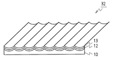
도 1은, 본 발명의 실시예 1의 액정 표시 장치에 적용되는 액정 표시 패널(1)을 부분적으로 확대하여 나타내는 단면도이다. 이 실시예의 액정 표시 장치는, 소위 투과형 또는 반사형이며, 이 도 1에서 액정 표시 패널(1)의 상측인 표면측 등에 편광판 등이 형성된다. 또한 투과형에서는 이 도 1에서 액정 표시 패널(1)의 하측인 배면측에 백라이트 장치가 형성되고, 반사형에서는, 이 도 1에서 액정 표시 패널(1)의 상측인 표면측에 프론트 라이트 장치가 형성된다.FIG. 1: is sectional drawing which expands and shows partially the liquid
이 액정 표시 패널(1)은, TFT 어레이 기판(2)과 CF 기판(3)에 의해 액정을 협지한다. 여기서 CF 기판(3)은, 투명한 절연 기판인 글래스 기판(4) 상에, 컬러 필터(5), 절연막(6), 투명 전극에 의한 전극(7), 배향막(8)을 순차적으로 형성하여 작성된다. 여기서 전극(7)은, 통상적으로는, ITO(Indium Tin Oxide)를 전체면에 성막하여 형성되지만, 화소마다 또는 서브 화소마다, 패터닝하여도 된다. 또한 배향막(8)은, 수평 배향을 유기하는 액정 배향재로서 가용성 폴리이미드와 폴리아믹산의 혼합물을 인쇄법에 의해 도포한 후, 200도의 온도에서 75분간 소성함으로써, 폴리이미드 박막을 막두께 50〔㎚〕에 의해 형성하고, 그 후, 러빙 처리에 의해 배향능을 부여하여 작성된다. 또한 러빙 처리의 방향은, 이 도면에서 화살표 방향이며, 후술하는 홈 M의 연장 방향과 직교하는 방향이다.The liquid
이것에 대하여 TFT 어레이 기판(2)은, 도 2에 도시하는 바와 같이, 투명의 절연 기판인 글래스 기판(10)에, TFT 등을 형성하여 절연막(11)을 형성하고, 이 절연막(11) 상에, 전극(12), 배향막(13)을 순차적으로 형성하여 작성된다.On the other hand, as shown in FIG. 2, the
TFT 어레이 기판(2)은, 배향막(13)을 작성하는 면의 형상이, 소정 방향으로 직선 형상으로 연장하는 홈이 이 소정 방향과 직교하는 방향으로 반복하여 형성된 홈 형상으로 되도록 형성되어, 이 홈 형상을 고분자막으로 피복하여 배향막(13)이 형성된다. 또한 이 실시예에서는, 절연막(11)의 표면 형상이 이 홈 형상으로 형성되어, 배향막(13)을 작성하는 면이 홈 형상으로 형성된다.The
여기서 홈 M은, 그 단면 형상이, 홈 M의 정점을 중심으로 한 대칭 형상의 대략 원호 형상으로 형성된다. 또한 홈 M은, 피치 P가 1〔㎛〕, 높이(깊이) H가 200〔㎚〕에 의해 형성되고, 이것에 의해 피치 P와 높이 H의 비 T(=H/P)가 1 미만의 0.2에 의해 형성된다.The groove M is formed in a substantially arc-shaped shape having a symmetrical shape centering on the vertex of the groove M here. The groove M has a pitch P of 1 [µm] and a height (depth) H of 200 [nm], whereby the ratio T (= H / P) of the pitch P and the height H is less than 0.2. Is formed by.
보다 구체적으로, TFT 어레이 기판(2)에서, 절연막(11)은, 노볼락계, 아크릴 계 등의 유기물 레지스트 재료, 혹은 Si02, SiN, 또는 Si02, SiN을 주성분으로 하는 무기계의 재료로 형성된다.More specifically, in the
여기서 감광성의 유기물 레지스트 재료로 절연막(11)을 형성하는 경우, TFT 어레이 기판(2)은, 감광성의 유기물 레지스트 재료를 코트한 후, 프리베이크하고, 그 후, 홈 M에 대응하는 패턴을 갖는 마스크를 이용하여 자외선 등에 의해 레지스트 재료를 노광한다. 또한 현상, 포토베이크하고, 이것에 의해 포토리소그래피법을 적용하여, 절연막(11)의 표면을 홈 형상으로 가공한다. 또한 마스크를 사용하는 대신에, 서로 다른 2방향으로부터 조사되는 광속의 간섭을 이용하여 노광 처리하여도 된다. 또한 포토리소그래피법 대신에, 나노 임프린트법 등의 방법을 적용하여도 된다.In the case where the insulating
또한 무기계 재료로, 절연막(11)을 형성하는 경우, TFT 어레이 기판(2)은, 진공 증착, 스퍼터, CVD 등에 의해, 이 무기계 재료를 소정막 두께로 퇴적시킨 후, 포토리소그래피법에 의해, 감광성 유기물 레지스트 재료를 홈 형상으로 패터닝하고, 그 후, 웨트 에칭 또는 드라이 에칭하여, 배향막(13) 측면을 홈 형상으로 한다. 또한 절연막(11)은, 일반적으로 시판되고 있는 무기계 재료와 유기계 재료의 혼합물로 감광성을 갖는 재료를 사용하여 작성할 수도 있고, 이 경우에는, 포토리소그래피법에 의해 패터닝한 후, 소성 등의 과정을 거침으로써, 유기물계의 성분이 분위기 중에 비산하고, 주로 무기물의 성분으로부터 절연막(11)이 형성된다.In the case where the insulating
또한 전극(12)은, 투과형에서는, 통상적으로는, ITO 등의 투명 전극 재료를 전체면에 성막한 후, 패터닝하여 형성된다. 또한 반사형에서는, 알루미늄, 은 등의 금속 재료를 적용하도록 하여도 된다.In the transmissive type, the
배향막(13)은, 일반적으로 사용되고 있는 폴리이미드계의 재료를, 오프셋법에 의해 도포한 후, 200도의 온도에서 75분간 소성하여 성막된다. 배향막(13)은, 이 소성의 처리에 의해, 배향막 중의 고분자쇄가 홈 M의 연장 방향과 직교하는 방향으로 배열되고, 배향능이 부여된다. 또한 배향막(13)의 도포법에는, 스핀 코트법, 감마 부틸락톤, 아세톤 등의 용매로 희석한 용액의 조 안에 담그는 디핑법, 스프레이것에 의해 분무하는 방법 등, 다양한 방법을 적용할 수 있다.The
여기서 배향막(13)은, 하층의 표면 형상을 홈 형상으로 한 상태에서, 배향재의 도포, 소성을 행하는 과정에서, 배향막 내의 고분자쇄의 방향이 홈 M의 연장 방향에 대하여 직교하는 방향과 일치되어, 배향능이 부여된다. 이것은 소성 시에서의 온도 상승, 온도 강하의 과정에서, 기판(10)이 팽창, 수축하고, 이 팽창, 수축에 의한 응력이 홈 형상에 의해 배향막(13)의 특정 방향에 작용하는 1축 연신 효과에 의해, 배향막 내의 고분자쇄가 이 직교하는 방향으로 배열되는 것이, 요인의 하나로서 생각된다.Here, the
다양하게 검토한 결과에 따르면, 이러한 도포 후의 소성에 의해 일정한 방향으로 분자축이 배열되기 위해서는, 배향막(13)의 하측면에, 이 일정 방향과 직교하는 방향으로 연장하는 홈 M이 형성되어 있는 것이 필요하며, 단순한 돌기, 요철에서는, 각 정점으로부터 끝자락을 향하는 방향으로 배향막의 분자축이 배열되어, 특정 방향에 배향능을 부여할 수 없다는 것을 알 수 있었다.According to various examination results, in order for the molecular axis to be arranged in a fixed direction by such post-firing, grooves M extending in the direction orthogonal to this constant direction are formed in the lower surface of the
또한 홈 M에 대해서는, 피치 P와 높이 H의 비 T(=H/P)가 1 미만인 경우에도, 충분히 배향능을 부여할 수 있고, 배향막(13)의 하측면을 홈 형상으로 가공하는 관점으로부터 보면, 피치 P와 높이 H의 비 T를 1 미만으로 하여, 더욱 바람직하게는, 피치 P와 높이 H의 비 T를 0.5 미만으로 하여, 생산성을 향상할 수 있다.Moreover, about the groove | channel M, even when ratio T (= H / P) of pitch P and height H is less than 1, an orientation capability can fully be provided and it is from a viewpoint of processing the lower surface of the
액정 표시 패널(1)은, TFT 어레이 기판(2), CF 기판(3)을 시일재로 접합한 후, 이들 TFT 어레이 기판(2), CF 기판(3) 간의 갭에, 플러스의 유전율 이방성을 갖는 네마틱 액정이 주입되어 형성된다. 또한 이 도 1에서는, 액정 분자를 참조 부호 15로 표시하고, θ, θ/2는, 액정 분자(15)의 틸트각이다. 이 경우, 액정을 주입하여 액정 분자(15)의 배향 방향을 확인한 바, TFT 어레이 기판(2) 측면에서는, 홈 M의 연장 방향과 직교하는 방향으로 액정 분자(15)가 배향하고 있고, 도 1에 도시하는 바와 같이, 홈 M의 연장 방향이 러빙 방향과 직교하도록 TFT 어레이 기판(2), CF 기판(3)을 접합한 경우에는, 액정 분자(15)가 호모지니어스 배향하는 것이 확인되었다. 또한 홈 M의 연장 방향이 러빙 방향과 평행하게 되도록 TFT 어레이 기판(2), CF 기판(3)을 접합한 경우에는, 액정 분자(15)가 트위스티드 네마틱 배향하는 것이 확인되었다.After the liquid
즉 도 4는, 도 3과의 대비에 의해, 액정 표시 패널(1)의 1화소(적색, 녹색, 청색의 서브 화소의 1조)의 편광 현미경에 의한 관측 결과를 나타내는 사진이며, 편광판을 크로스니콜 배치로 하고, 그 사이에, 호모지니어스 배향시킨 액정 표시 패널(1)을 배치하여 관측한 경우이다. 또한 액정 표시 패널(1)은, 광학축이 편광자의 흡수축과 평행하게 되도록 배치하였다. 또한 도 3은, TFT 어레이 기판(2) 측 의 배향막(13)을 생략하여 이 액정 표시 패널(1)과 동일하게 구성한, 단순히 탄성 왜곡 효과만을 이용하여 액정 분자를 배향시키는 종래의 그레이팅법에 의한 액정 표시 패널의, 도 4와 동일한 조건에 의한 관측 결과이다.That is, FIG. 4 is a photograph which shows the observation result by the polarization microscope of one pixel (one set of red, green, and blue subpixel) of the liquid
이 경우, 액정 표시 패널(1)의 광학축이 완전하게 배열되어 있으면, 편광자로부터 입사한 광에 위상 변화가 발생하지 않게 되고, 흑으로서 관찰되게 된다. 그러나, 국소적으로 광학축이 어긋나 있으면, 그레이 혹은 백의 모양으로서 관찰되게 된다.In this case, when the optical axis of the liquid
도 3 및 도 4의 관측 결과에 의하면, 도 4 쪽이, 보다 검게 관찰되어 있기 때문에, 단순히 탄성 왜곡 효과만을 이용하여 액정 분자를 배향시키는 종래의 그레이팅법에 의한 액정 표시 패널에 비하여, 이 실시예의 액정 표시 패널(1) 쪽이, 배향 규제력이 높다고 판단할 수 있다.According to the observation results of FIG. 3 and FIG. 4, since FIG. 4 is observed blacker, compared with the liquid crystal display panel by the conventional grating method which orientates a liquid crystal molecule only using an elastic distortion effect, The liquid
또한 이 실시예의 액정 표시 패널(1)에서는, 홈의 피치 P와 높이 H의 비 T가, 1 이하인 0.2이기 때문에, 이 비가 1 이상 필요한 단순히 탄성 왜곡 효과만을 이용하여 액정 분자를 배향시키는 종래의 그레이팅법에 비하여, 각별히 홈 M의 작성 공정을 간략화하여 높은 생산성을 확보할 수 있다. 또한 다양한 특성이 우수한 재료를 적용하여 생산할 수 있고, 나아가서는 간이하고도 확실하게 배향능을 부여할 수 있음으로써, 그레이팅법에서, 배향막재 자체가 갖는 배향 규제력을 이용하는 종래 구성의 여러 가지 문제점도 유효하게 회피할 수 있다.Further, in the liquid
또한 도 3 및 도 4의 관찰 결과로부터, 이 실시예의 액정 표시 패널(1)에서는, TFT 어레이 기판(2) 측에서 홈 M의 연장 방향과 직교하는 방향으로 액정 분자 가 배향하고 있는 것에 대하여, 종래의 그레이팅법에 의한 액정 표시 패널에서는, TFT 어레이 기판(2) 측에서 홈 M의 연장 방향과 평행 방향으로 액정 분자가 배향하고 있는 것을 확인할 수 있었다. 이것에 의해 이 실시예의 배향막(13)에 의한 액정 분자(15)의 배향이, 탄성 왜곡 효과를 이용하는 종래의 그레이팅법에 의한 것과는 상이한 것을 확인할 수 있었다.3 and 4 show that in the liquid
또한 호모지니어스 배향하고 있는 액정 셀의 틸트각을 크리스탈 로테이션법에 의해 측정한 바, 약 1.5도이었다. 여기서 TFT 어레이 기판(2) 및 CF 기판(3)을 함께 러빙 처리한 경우의 액정 셀의 틸트각이 약 3도이기 때문에, 이 실시예에 의한 액정 표시 패널(1)에서는, CF 기판(3)의 표면에서의 틸트각 θ가 3도이며, TFT 어레이 기판(2)의 표면에서의 틸트각이 0도라고 생각된다.Moreover, it was about 1.5 degree when the tilt angle of the homogeneous orientation liquid crystal cell was measured by the crystal rotation method. Since the tilt angle of the liquid crystal cell when the
도 5는, 이 액정 표시 패널(1)에 전압을 인가한 경우의 모식도이다. 이 액정 표시 패널(1)은, 전압을 인가하여도, TFT 어레이 기판(2), CF 기판(3)의 계면 근방에서는, 액정 분자의 배향은 변화하지 않고, 계면으로부터 멀어짐에 따라서 서서히 액정 분자(15)의 틸트각이 커지고, TFT 어레이 기판(2) 및 CF 기판(3) 간의 중앙 부분에서, 틸트각이 약 90도로 되어 최대로 된다.5 is a schematic diagram when a voltage is applied to the liquid
이 전압 인가 시의 리터데이션을 회전 검광자법에 의해 측정하고, TFT 어레이 기판(2), CF 기판(3)을 함께 러빙 처리한 액정 셀의 리터데이션과 비교하였다. 여기서 앵커링 강도가 약한 경우에는, 전압의 인가에 의해, TFT 어레이 기판(2)측 계면에서의 액정 분자의 틸트각이 변화하기 때문에, TFT 어레이 기판(2), CF 기판(3)을 함께 러빙 처리한 액정 셀에 비하여 리터데이션이 작아진다. 그러나 측정 한 결과에 의하면, 전압 인가시, 이 실시예의 액정 표시 패널(1)은, TFT 어레이 기판(2), CF 기판(3)을 함께 러빙 처리한 액정 셀과 거의 동등한 리터데이션이 측정되고, 이것에 의해 TFT 어레이 기판(2) 측의 배향막(13)에 의해, 충분한 앵커링 강도를 확보하고 있는 것을 확인할 수 있었다.The retardation at the time of voltage application was measured by the rotational analyzer method, and it compared with the retardation of the liquid crystal cell which rubbed the
또한 이 도 1의 예에서는, TFT 어레이 기판(2)의 배향막(13) 및 CF 기판(3)의 배향막(8)에 각각 홈 형상 및 러빙 처리에 의해 배향능을 부여하는 경우에 대하여 설명하였지만, 본 실시예는 이것에 한하지 않고, 이것과는 반대로, TFT 어레이 기판(2)의 배향막(13) 및 CF 기판(3)의 배향막(8)을 각각 러빙 처리 및 홈 형상에 의해 배향능을 부여하여도 되며, 또한 TFT 어레이 기판(2) 및 CF 기판(3)의 배향막(8, 13)의 쌍방에 홈 형상에 의해 배향능을 부여하여도 된다. 또한 이 도 1의 예에서는, 네마틱 액정을 적용하는 경우에 대하여 설명하였지만, 스멕틱, 콜레스테릭 등, 여러 가지의 액정을 널리 적용할 수 있다.In addition, in the example of FIG. 1, the case where the alignment capability is imparted to the
(2) 실시예의 효과(2) Effect of Example
이상의 구성에 의하면, 액정을 협지하여 대향하는 2개의 기판(2, 3) 중 적어도 1개의 기판(2)에서, 배향막(13)을 작성하는 면의 형상을, 소정 방향으로 연장하는 홈 M이 이 소정 방향과 직교하는 방향으로 반복하여 형성된 홈 형상으로 하고, 이 홈 형상을 고분자막으로 피복하여 배향막(13)을 형성함으로써, 종래에 비하여 생산성이 높으며, 충분한 앵커링 강도 및 화질을 확보할 수 있다.According to the above structure, in the at least 1 board |
즉 이 1개의 기판에서, 고분자쇄가 이 직교하는 방향으로 배열되도록 배향막(13)을 형성함으로써, 단순히 탄성 왜곡 효과를 이용하는 종래의 그레이팅법에 비하여, 홈의 깊이를 얕게 하여 충분한 앵커링 강도를 확보할 수 있어, 생산성을 향상할 수 있다.In other words, by forming the
또한 홈에 의한 1축 연신 효과에 의해, 고분자쇄가 이 직교하는 방향으로 배열되도록 형성함으로써, 간이하게 배향능을 부여할 수 있다.Moreover, by forming the polymer chain so that it may be arranged in this orthogonal direction by the uniaxial stretching effect by a groove | channel, orientation ability can be provided simply.
또한 홈의 깊이를 홈의 피치로 나눈 값이 1 미만임으로써, 높은 생산성을 확보할 수 있다.In addition, since the value obtained by dividing the depth of the groove by the pitch of the groove is less than 1, high productivity can be ensured.
또한 이 1개의 기판 표면에서, 이 직교하는 방향으로 액정의 분자가 배향하도록 설정함으로써, 네마틱 액정, 스멕틱, 콜레스테릭 등, 여러 가지의 액정을 널리 적용할 수 있다.Moreover, various liquid crystals, such as nematic liquid crystal, smectic, and cholesteric, can be applied widely by setting so that the molecule | numerator of a liquid crystal may orientate in this orthogonal direction on this one board | substrate surface.
또한 글래스 기판(10) 및 전극(12) 간에 형성된 절연막(11)의 표면 형상을 홈 형상으로 하여, 배향막(13)을 작성하는 면의 형상을 홈 형상으로 함으로써, 절연막(11)을 가공하는 다양한 방법을 널리 적용하여, 종래에 비하여 생산성이 높고, 충분한 앵커링 강도, 화질을 확보할 수 있다.In addition, the surface shape of the insulating
<실시예 2><Example 2>
도 6은, 도 2와의 대비에 의해 본 발명의 실시예 2에 적용되는 액정 표시 패널의 TFT 어레이 기판을 나타내는 사시도이다. 이 TFT 어레이 기판(22)은, 절연막(11)의 표면 형상 대신에, 전극(12)의 표면 형상이 홈 형상으로 형성되어, 배향막(13)을 작성하는 면의 형상이 홈 형상으로 형성된다. 이 실시예의 액정 표시 패널은, 이 홈 형상의 가공에 관한 점이 상이한 점을 제외하고, 실시예 1의 액정 표시 패널(1)과 동일하게 형성된다.FIG. 6 is a perspective view illustrating a TFT array substrate of a liquid crystal display panel applied to
즉 이 실시예에 따른 TFT 어레이 기판(22)은, 실시예 1에 대하여 전술한 것과 마찬가지로 하여 글래스 기판(10) 상에 일정한 막 두께에 의해 절연막(11)이 형성된다. 또한 계속해서, ITO, 알루미늄, 은 등을 성막한 후, 포토리소그래피법에 의해 감광성 레지스트를 홈 형상으로 패터닝하고, 웨트 에칭 처리 또는 드라이 에칭 처리하여 전극(12)에 홈 형상이 형성된다. 또한 실시예 1에 대하여 전술한 것과 마찬가지로, 도 6에 도시하는 구성을 CF 기판측에 적용하여도 된다.That is, in the
이 실시예와 같이, 절연막의 표면 형상 대신에, 전극(12)의 표면 형상을 홈 형상으로 하여, 배향막을 작성하는 면의 형상을 홈 형상으로 하여도, 실시예 1과 마찬가지의 효과를 얻을 수 있다.As in this embodiment, the same effect as in Example 1 can be obtained even when the surface shape of the
<실시예 3><Example 3>
도 7은, 도 2와의 대비에 의해 본 발명의 실시예 3의 액정 표시 장치에 적용되는 액정 표시 패널의 TFT 어레이 기판을 나타내는 사시도이다. 이 TFT 어레이 기판(32)은, 절연막(11)의 표면 형상 대신에, 절연 기판인 글래스 기판(10)의 표면 형상이 직접, 홈 형상으로 되어, 배향막(13)을 작성하는 면의 형상이 홈 형상으로 형성된다. 이 실시예의 액정 표시 패널은, 이 홈 형상의 가공에 관한 점이 상이한 점을 제외하고, 실시예 1의 액정 표시 패널(1)과 동일하게 형성된다. 또한 이 도 7의 예에서는, 절연막이 생략되어 있지만, 필요에 따라서 절연막을 형성하도록 하여도 된다.FIG. 7 is a perspective view illustrating a TFT array substrate of a liquid crystal display panel applied to the liquid crystal display device of
즉 TFT 어레이 기판(32)은, 글래스 기판(10)의 표면측에서, 포토리소그래피법에 의해 감광성 레지스트를 홈 형상으로 패터닝한 후, 웨트 에칭 처리 또는 드라 이 에칭 처리하고, 글래스 기판(10)의 표면측이 홈 형상으로 가공된다. 그 후, 전극(12), 배향막(13)이 순차적으로 작성된다. 또한 실시예 1에 대하여 전술한 것과 마찬가지로, 도 7에 도시하는 구성을 CF 기판측에 적용하여도 된다.That is, the
이 실시예와 같이, 절연막의 표면 형상 대신에, 절연 기판의 표면 형상을 홈 형상으로 하여, 배향막을 작성하는 면의 형상을 홈 형상으로 하여도, 실시예 1과 마찬가지의 효과를 얻을 수 있다.As in this embodiment, the same effect as in Example 1 can be obtained even when the surface shape of the insulating substrate is made into the groove shape instead of the surface shape of the insulating film, and the shape of the surface on which the alignment film is formed is made into the groove shape.
<실시예 4><Example 4>
도 8은, 도 1과의 대비에 의해 본 발명의 실시예 4의 액정 표시 장치에 적용되는 액정 표시 패널을 나타내는 단면도이다. 이 실시예의 액정 표시 패널(41)은, TFT 어레이 기판(42)에 형성되는 홈 M의 단면 형상이 상이한 점, 및 CF 기판(43) 측에도 TFT 어레이 기판(42)과 마찬가지의 홈 형상이 형성되는 점을 제외하고, 실시예 1~3의 액정 표시 패널과 동일하게 구성된다. 또한 이 도 8, 후술하는 도 9 및 도 10에서는, 이해의 편의를 돕기 위하여, 실시예 1과 마찬가지로, 절연막(6, 11)의 표면 형상을 홈 형상으로 하는 도면을 도시한다.FIG. 8 is a cross-sectional view showing a liquid crystal display panel applied to the liquid crystal display device of Example 4 of the present invention in contrast with FIG. 1. In the liquid
즉 도 9에 도시하는 바와 같이, TFT 어레이 기판(42)에서는, 홈 M을 가로지르는 방향의 단면 형상이, 홈 M의 정점을 중심으로 하여 비대칭 형상으로 형성되고, 이것에 의해 액정 표시 패널(41)은, TFT 어레이 기판(42)의 표면에서의 액정 분자(15)의 틸트각을, 이 비대칭 형상으로 결정되는 각도로 제어한다.That is, as shown in FIG. 9, in the
즉 이 실시예에서, TFT 어레이 기판(42)은, 단면 형상이 톱니 형상으로 되도록 홈 M이 형성되고, 이것에 의해 한 쌍의 사면 M1 및 M2에 의한 단면 삼각형 형상 의 돌조가 순차적으로 소정 피치로 반복되도록, 홈 형상이 형성된다. 이것에 의해 TFT 어레이 기판(42)은, 글래스 기판(10)의 표면과 평행한 면 H에 대한 이 1쌍의 사면 M1 및 M2가 이루는 각도 θ1, θ2가 서로 다른 각도로 설정되어, 액정 분자(15)의 틸트각이 제어된다. 또한 홈의 단면 형상은, 이 도 9에 도시하는 바와 같이, 단면 형상을 톱니 형상으로 하는 경우에 한하지 않고, 예를 들면 홈 M의 정점을 한쪽 측으로 기울어지게 하여 비대칭 형상으로 하는 경우 등, 요컨대, 비대칭 형상으로 홈을 형성하여 액정 분자(15)의 틸트각을 다양하게 제어할 수 있다.That is, in this embodiment, the grooves M are formed in the
보다 구체적으로, 이 실시예에서, 홈 M은, 피치 P가 1〔㎛〕, 높이 H가 200〔㎚〕으로 형성되고, 각도 θ1이 3도로 설정된다. 또한 실시예 1과 마찬가지로, 폴리이미드계의 재료를 도포한 후, 200도의 온도에서 75분간 소성하여 50〔㎚〕에 의해 배향막(13)을 성막하였다. 또한 CF 기판(43)에 대해서도, TFT 어레이 기판(42)과 동일하게 홈 형상을 형성한 후, 배향막(8)을 형성하였다.More specifically, in this embodiment, the groove M has a pitch P of 1 [mu] m, a height H of 200 [nm], and an angle [theta] 1 being set to 3 degrees. In addition, similarly to Example 1, after apply | coating a polyimide-type material, it baked for 75 minutes at the temperature of 200 degreeC, and formed the
이 실시예의 액정 표시 패널(41)은, TFT 어레이 기판(42), CF 기판(43)을 시일재로 접합한 후, 이들 TFT 어레이 기판(42), CF 기판(43) 간의 갭에, 플러스의 유전율 이방성을 갖는 네마틱 액정이 주입되어 형성된다.In the liquid
여기서 실시예 1에 대하여 전술한 것과 마찬가지로 하여 액정 분자(15)의 배향 방향을 확인한 바, 홈 M이 연장하는 방향과 직교하는 방향으로 배향하고 있는 것을 확인할 수 있었다. 또한 도 8에 도시하는 바와 같이, TFT 어레이 기판(42)에서의 톱니 형상의 연속하는 방향과, CF 기판(43)에서의 톱니 형상의 연속하는 방향이 역방향으로 되도록, TFT 어레이 기판(42), CF 기판(43)을 접합한 경우, 호모지 니어스 배향으로 되고, TFT 어레이 기판(42)에서의 톱니 형상의 연속하는 방향과, CF 기판(43)에서의 톱니 형상의 연속하는 방향이 동일한 방향으로 되도록, TFT 어레이 기판(42), CF 기판(43)을 접합한 경우, π 배향하는 것이 확인되었다.When the orientation direction of the
도 10은, 이 액정 표시 패널(41)에 전압을 인가한 경우의 모식도이다. 이 액정 표시 패널(41)은, 전압을 인가하여도, TFT 어레이 기판(42), CF 기판(43)의 계면 근방에서는, 액정 분자의 배향은 변화하지 않고, 계면으로부터 멀어짐에 따라서 서서히 액정 분자(15)의 틸트각이 커지고, TFT 어레이 기판(42) 및 CF 기판(43) 간의 중앙 부분에서, 틸트각이 약 90도로 되어 최대로 된다. 액정 표시 패널(41)은, 이 상태에서 TFT 어레이 기판, CF 기판을 함께 러빙 처리한 액정 셀과 거의 동등한 리터데이션이 측정되고, 이것에 의해 충분한 앵커링 강도를 확보하고 있는 것을 확인할 수 있었다.10 is a schematic diagram when a voltage is applied to the liquid
이상의 구성에 의하면, 홈을 가로지르는 방향의 단면 형상을, 홈의 정점을 중심으로 하여 비대칭 형상으로 형성함으로써, 액정 분자의 틸트각을 여러 가지로 제어할 수 있다.According to the above structure, the tilt angle of a liquid crystal molecule can be controlled in various ways by forming the cross-sectional shape of the direction crossing a groove to an asymmetric shape centering on the vertex of a groove.
<실시예 5><Example 5>
도 11은, 도 1과의 대비에 의해 본 발명의 실시예 5의 액정 표시 장치에 적용되는 액정 표시 패널을 나타내는 단면도이다. 이 실시예의 액정 표시 패널(51)은, 플러스의 유전율 이방성을 갖는 네마틱 액정 대신에, 마이너스의 유전율 이방성을 갖는 네마틱 액정이 TFT 어레이 기판(2) 및 CF 기판(3) 간에 주입되는 점, 호메오트로픽 배향을 유기하는 배향막을 사용하는 점을 제외하고, 실시예 1~3의 액정 표시 패널(1)과 동일하게 구성된다. 또한 이 도 11, 후술하는 도 12에서는, 이해를 용이하게 하기 위해, 실시예 1과 마찬가지로, 절연막(11)의 표면 형상을 홈 형상으로 하는 도면을 도시한다.FIG. 11 is a cross-sectional view showing a liquid crystal display panel applied to the liquid crystal display device of Example 5 of the present invention in contrast with FIG. 1. In the liquid
이 경우, 액정 분자(55)가, 액정 표시 패널(51)의 두께 방향으로 배향하여, 호메오트로픽 배향하고 있는 것이 확인되었다.In this case, it was confirmed that the
여기서 도 12는, 이 액정 표시 패널(51)에 전압을 인가한 경우의 모식도이다. 이 액정 표시 패널(51)은, 전압을 인가하여도, TFT 어레이 기판(2), CF 기판(3)의 계면 근방에서는, 액정 분자(55)의 배향은 변화하지 않고, 계면으로부터 멀어짐에 따라서 서서히 액정 분자(55)의 틸트각이 작아지고, TFT 어레이 기판(2) 및 CF 기판(3) 간의 중앙 부분에서, 틸트각이 약 0도로 되어 최소로 된다. 이 틸트각이 약 0도로 되는 액정 분자(55)의 배향 방향이, 홈의 연장 방향과 직교하는 방향이며, 틸트의 방향이 러빙 방향에 의해 결정되는 것을 확인할 수 있었다.12 is a schematic diagram when a voltage is applied to the liquid
이 실시예에 의하면, 마이너스의 유전율 이방성을 갖는 네마틱 액정을 적용하도록 하여도, 전술한 실시예와 마찬가지의 효과를 얻을 수 있다.According to this embodiment, even if a nematic liquid crystal having negative dielectric anisotropy is applied, the same effects as in the above embodiment can be obtained.
<실시예 6><Example 6>
도 13 및 도 15는, 도 8 및 도 10과의 대비에 의해 본 발명의 실시예 6의 액정 표시 장치에 적용되는 액정 표시 패널을 나타내는 단면도이다. 이 실시예의 액정 표시 패널(61)은, 플러스의 유전율 이방성을 갖는 네마틱 액정 대신에, 마이너스의 유전율 이방성을 갖는 네마틱 액정이 TFT 어레이 기판(42) 및 CF 기판(43) 간에 주입되는 점, 호메오트로픽 배향을 유기하는 배향막을 사용하는 점을 제외하고, 실시예 4의 액정 표시 패널(41)과 동일하게 구성된다. 또한 이 도 13 및 도 14에서는, 이해의 편의를 돕기 위하여, 도 8과 마찬가지로, 절연막(6, 11)의 표면 형상을 홈 형상으로 하는 도면을 도시한다.13 and 15 are cross-sectional views showing a liquid crystal display panel applied to the liquid crystal display device of the sixth embodiment of the present invention in contrast with FIGS. 8 and 10. In the liquid
이 경우에도, 실시예 5와 마찬가지로, 액정 분자(55)가, 액정 표시 패널(61)의 두께 방향으로 배향하여, 호메오트로픽 배향하고 있는 것이 확인되었다. 또한 TFT 어레이 기판(42), CF 기판(43)의 계면 근방에서는, 홈 형상으로 결정되는 방향의 틸트각으로, 글래스 기판(4, 10)의 표면에 대하여 수직 방향으로 배향하고 있는 것이 확인되었다.Also in this case, it was confirmed that
또한 전압을 인가하여도, TFT 어레이 기판(42), CF 기판(43)의 계면 근방에서는, 액정 분자(55)의 배향은 변화하지 않고, 계면으로부터 멀어짐에 따라서 서서히 액정 분자(55)의 틸트각이 작아지고, TFT 어레이 기판(42) 및 CF 기판(43) 간의 중앙 부분에서, 틸트각이 약 0도로 되어 최소로 된다. 이 틸트각이 약 0도로 되는 액정 분자(55)의 배향 방향은, 홈의 연장 방향과 직교하는 방향인 것을 확인할 수 있었다.Even when a voltage is applied, the orientation of the
이 실시예에 의하면, 마이너스의 유전율 이방성을 갖는 네마틱 액정을 적용하도록 하여도, 전술한 실시예 4와 마찬가지의 효과를 얻을 수 있다.According to this embodiment, even if a nematic liquid crystal having negative dielectric anisotropy is applied, the same effects as those of the fourth embodiment described above can be obtained.
<실시예 7><Example 7>
도 15는, 본 발명의 실시예 7의 액정 표시 장치에 적용되는 액정 표시 패널의 1 화소의 개략적인 구성을 나타내는 평면도이고, 도 16은, 이 액정 표시 패널(71)을 A-A선으로 절취하여 나타내는 상세한 단면도이다. 또한 이 도 15는, CF 기판(73)에 형성된 홈 M을 액정 분자(15)와 함께 나타내는 도면이다.FIG. 15 is a plan view showing a schematic configuration of one pixel of a liquid crystal display panel applied to the liquid crystal display device of the seventh embodiment of the present invention, and FIG. 16 shows the liquid
이 액정 표시 패널(71)은, 소위 반투과형이며, 1개의 화소 내에 반사 표시부(74)와 투과 표시부(75)가 형성되고, TFT 어레이 기판(72)의 하면에, 1/4 파장판(76), 1/2 파장판(77), 편광판(78)이 순차적으로 형성된다. 또한 CF 기판(73)의 상면에, 1/4 파장판(79), 1/2 파장판(80), 편광판(81)이 순차적으로 형성된다.The liquid
여기서 TFT 어레이 기판(72)은, 글래스 기판(10)에, 순차적으로, 절연막(11), 전극(12), 배향막(13)을 형성한 후, 러빙 처리하여 배향막(13)에 배향능이 부여된다. 또한 반사 표시부(74)에서는, 입사광을 산란시키도록, 절연막(11)에 요철 형상이 형성되어, 전극(12), 배향막(13)의 표면측이 요철 형상으로 형성된다.Here, the
또한 CF 기판(73)은, 글래스 기판(4)에, 컬러 필터(5), 절연막(6), 전극(7), 배향막(8)이 순차적으로 형성되고, 실시예 1~4에 대하여 전술한 TFT 어레이 기판과 마찬가지로, 배향막(8)을 형성하는 면의 형상을 홈 형상으로 함으로써, 배향막(8)에 배향능이 부여된다.In the
여기서 이 액정 표시 패널(71)에서, 반사 표시부(74), 투과 표시부(75)는, 동일한 축각도, 리터데이션의 광학 설계가 이루어지고, TFT 어레이 기판(72) 및 CF 기판(73) 간의 갭이 동일 간격으로 설정된다. 또한 투과 표시부(75)에서는, CF 기판(73)에 형성된 홈 M의 연장 방향이, TFT 어레이 기판(72)에서의 러빙 방향과 일치하도록 설정되는 것에 대하여, 반사 표시부(74)에서는, CF 기판(73)에 형성된 홈 M의 연장 방향이 TFT 어레이 기판(72)에서의 러빙 방향에 대하여 비스듬하게 기운 방향으로 되도록 설정된다.Here, in the liquid
이것에 의해 이 액정 표시 패널(71)은, 반사 표시부(74) 및 투과 표시부(75)에서, TFT 어레이 기판(72) 및 CF 기판(73) 간의 갭에 단차를 형성하지 않고, 1개의 화소 내에서 서로 다른 배향을 간이하게 확보할 수 있다. 또한 이 실시예에서는, 투과 표시부(75)는 호모지니어스 배향으로 하고, 반사 표시부(74)는 50도 트위스트 배향으로 하였다. 또한 반사 표시부(74)의 트위스트 각도는, 50도에 한하지 않고, 40도~70도의 범위에서, 반투과형 액정 표시 패널(71)을 구성할 수 있다. 따라서 이 실시예에서는, 투과 표시부(75)에서의 홈 M의 연장 방향에 대하여, 반사 표시부(74)에서의 홈 M의 연장 방향이 50도의 각도로 되도록 설정되어 있지만, 이 각도는, 40도~70도의 범위에서, 실용적으로 사용할 수 있다.As a result, the liquid
즉 반투과형의 액정 표시 패널에서, 투과 표시부에서는, 배면으로부터 입사한 광이 단지 액정을 투과하여 출사되는 것에 대하여, 반사 표시부에서는, 입사광이 액정을 왕복하게 된다. 이것에 의해 투과 표시부와 반사 표시부에서 출사광에 동일한 위상차를 부여하기 위해서는, 투과 표시부에 비하여, 반사 표시부의 갭을 1/2의 간격으로 설정하는 것이 필요하게 되고, 투과 표시부와 반사 표시부에서, TFT 어레이 기판 및/또는 CF 기판의 액정 측면에 단차를 형성하는 것이 필요하게 된다.That is, in the transflective liquid crystal display panel, in the transmissive display portion, the incident light reciprocates the liquid crystal in the reflective display portion, whereas the light incident from the rear side passes through the liquid crystal. As a result, in order to give the same phase difference to the emitted light in the transmission display unit and the reflection display unit, it is necessary to set the gap of the reflection display unit at an interval of 1/2 compared to the transmission display unit, and in the transmission display unit and the reflection display unit, It is necessary to form a step on the liquid crystal side of the array substrate and / or the CF substrate.
그러나 이와 같이 단차를 형성하는 경우에는, 공정이 번잡하게 되어, 생산성이 저하한다. 또한 단차에 의해 광 누설이 발생하여, 콘트라스트가 저하되는 문제도 있다. 또한, 광 누설에 대해서는, 투과 표시부의 반사 표시부측 경계를 금속 전극으로 피복하여 차광하는 방법도 있지만, 이 경우, 표시에 사용하지 않는 무효 한 영역이 발생함으로써, 고정밀화의 장해로 된다.However, when forming a step | step in this way, a process becomes complicated and productivity falls. In addition, there is a problem that light leakage occurs due to a step, and contrast is lowered. In addition, in light leakage, there is also a method of covering and shielding the reflective display side boundary of the transmissive display portion with a metal electrode, but in this case, an invalid area not used for display is generated, which leads to high precision.
그러나 이 실시예에 의하면, 이러한 단차를 형성하지 않아도 됨으로써, 간이한 공정으로, 고반사율 및 고개구율의 액정 표시 패널을 구성할 수 있다.However, according to this embodiment, it is not necessary to form such a step | step, and a liquid crystal display panel of a high reflectance and a high opening ratio can be comprised by a simple process.
또한 이 실시예에서는, CF 기판(73) 측에서, 홈 형상에 의해 배향막에 배향능을 부여하는 경우에 대하여 설명하였지만, 이 대신에 TFT 어레이 기판(72) 측에서, 홈 형상에 의해 배향막에 배향능을 부여하도록 하여도 되며, 또한 CF 기판(73) 및 TFT 어레이 기판(72)의 쌍방에서, 홈 형상에 의해 배향막에 배향능을 부여하도록 하여도 된다. 또한 CF 기판(73) 및 TFT 어레이 기판(72)의 쌍방에서, 홈 형상에 의해 배향막에 배향능을 부여하는 경우에는, CF 기판(73) 및 TFT 어레이 기판(72)의 쌍방에서, 또는 한쪽에서, 투과 표시부에서의 홈의 연장 방향에 대하여 반사 표시부에서의 홈의 연장 방향을 기울이도록 할 수 있다.In this embodiment, the case where the alignment capability is imparted to the alignment film by the groove shape on the
또한 이와 같이 CF 기판(73) 및 또는 TFT 어레이 기판(72)에서, 홈 형상에 의해 배향막에 배향능을 부여하는 경우에는, 실시예 4에 대하여 전술한 바와 같이, 홈의 단면 형상을 비대칭 형상으로 하여 틸트각을 제어하도록 하여도 된다.In the
또한 실시예 5, 6에 대하여 전술한 바와 같이, 플러스의 유전율 이방성을 갖는 액정 대신에, 마이너스의 유전율 이방성을 갖는 액정을 적용하도록 하여도 된다.As described above with respect to Examples 5 and 6, instead of the liquid crystal having positive dielectric anisotropy, a liquid crystal having negative dielectric anisotropy may be applied.
또한 1개의 화소를 구성하는 서브 화소마다, 투과 표시부 및 또는 반사 표시부에서 홈 M의 기울기를 변화시켜, 서브 화소마다, 광학 특성을 최적화하도록 하여도 된다. 또한 이와 같이 서브 화소마다, 광학 특성을 최적화하는 구성에서는, 반 투과형 액정 표시 패널에 한하지 않고, 투과형 액정 표시 패널, 반사형 액정 표시 패널에 적용할 수도 있다. 즉 예를 들면 CF 기판 및 TFT 어레이 기판 간의 갭을 녹색에 대하여 최적화한 경우, 청색에서는 갭의 간격이 지나치게 크고, 적색에서는 갭의 간격이 지나치게 짧게 된다. 따라서 이 경우, 녹색의 서브 화소에 대하여 청색 및 적색의 서브 화소에서 각각 홈의 연장 방향을 기울임으로써, 서브 화소마다, 광학 특성을 최적화할 수 있다.In addition, the inclination of the grooves M may be changed in the transmissive display section or the reflective display section for each sub-pixel constituting one pixel to optimize the optical characteristics for each sub-pixel. In this configuration, the optical characteristics of each sub-pixel are not limited to the semi-transmissive liquid crystal display panel but can be applied to the transmissive liquid crystal display panel and the reflective liquid crystal display panel. That is, for example, when the gap between the CF substrate and the TFT array substrate is optimized for green, the gap gap is too large in blue, and the gap gap is too short in red. In this case, therefore, the optical characteristics can be optimized for each subpixel by tilting the extension direction of the grooves in the blue and red subpixels, respectively, with respect to the green subpixels.
이상의 구성에 의하면, 1개의 화소를 투과 표시부와 반사 표시부로 형성하고, 투과 표시부에서의 홈의 연장 방향에 대하여, 반사 표시부에서의 홈의 연장 방향을 기울임으로써, 간이한 공정으로, 고화질의 반투과형 액정 표시 패널을 얻을 수 있다.According to the above structure, one pixel is formed by the transmissive display part and the reflective display part, and the inclination direction of the groove | channel in the reflective display part is inclined with respect to the extension direction of the groove | channel in the transmissive display part, and it is a simple process, and it is a semi-transmissive type of high quality. A liquid crystal display panel can be obtained.
<실시예 8><Example 8>
도 17은, 도 2와의 대비에 의해 본 발명의 실시예 8의 액정 표시 장치에 적용되는 TFT 어레이 기판(92)의 구성을 나타내는 사시도이다. 이 TFT 어레이 기판(92)은, 일정한 피치 P에 따른 홈 M이 일정 개수 이상 연속하지 않도록 하여, 홈 M이 형성된다. 보다 구체적으로, TFT 어레이 기판(92)은, 연속하는 홈 M에서 피치 P가 랜덤하게 변화하도록 설정된다. 이것에 의해 TFT 어레이 기판(92)은, 연속하는 홈 M이 회절 격자로서 기능하지 않도록 설정된다. 이 실시예의 액정 표시 패널은, 이 TFT 어레이 기판(92)에서의 피치 P의 설정이 상이한 점을 제외하고, 전술한 각 실시예와 동일하게 구성된다.FIG. 17 is a perspective view showing the structure of a
즉 일정한 피치 P에 의해 홈 M을 형성한 경우에는, 이 주기적인 홈 M이 회절 격자로서 기능하게 되어, 무지개색의 간섭 줄무늬가 간파되어, 화질이 현저하게 열화한다. 투과형 액정 표시 패널의 경우, 배향막이 굴절률 대략 1.5의 액정과 접하고 있기 때문에, 공기 중에 홈 M이 노출되어 있는 경우 정도는 아니지만, ITO 등의 투명 전극의 굴절률이 대략 2이기 때문에, 무지개색의 간섭 줄무늬가 발생한다. 또한 반사형 액정 표시 패널에서는, 무지개색의 간섭 줄무늬가 현저하게 된다.In other words, when the grooves M are formed at a constant pitch P, the periodic grooves M function as diffraction gratings, iridescent interference fringes are detected, and image quality is significantly degraded. In the case of the transmissive liquid crystal display panel, since the alignment film is in contact with the liquid crystal having a refractive index of approximately 1.5, the refractive index of the transparent electrode such as ITO is approximately 2, although the groove M is exposed in the air. Occurs. In the reflective liquid crystal display panel, iridescent interference fringes are remarkable.
그러나 이 실시예와 같이, 피치 P를 랜덤하게 변화시키고, 일정한 피치 P에 따른 홈 M이 일정 개수 이상 연속하지 않도록 설정하면, 이러한 무지개색의 간섭 줄무늬의 발생을 방지하여 화질의 열화를 방지할 수 있다.However, as in this embodiment, if the pitch P is changed randomly and the grooves M according to the constant pitch P are set not to be continuous for a predetermined number or more, such iridescent interference fringes can be prevented from occurring, thereby preventing deterioration of image quality. .
또한 이 실시예에서는, TFT 어레이 기판측에 홈 형상을 형성하여 배향능을 부여하는 경우에 대하여 설명하였지만, 이 무지개색의 간섭 줄무늬의 방지 방법은, 전술한 각 실시예, 나아가서는 이하에 설명하는 각 실시예 중 어느 것에나 적용할 수 있다.In this embodiment, a case has been described in which a groove shape is formed on the TFT array substrate side to impart orientation capability. However, this rainbow color interference fringe prevention method is described in each of the above-described embodiments and further described below. It can be applied to any of the embodiments.
이 실시예에서는, 일정한 피치에 따른 홈이 일정 개수 이상 연속하지 않도록, 피치를 가변함으로써, 무지개색의 간섭 줄무늬의 발생을 방지하여 화질의 열화를 방지할 수 있다.In this embodiment, by varying the pitch so that grooves according to a constant pitch are not continuous for a predetermined number or more, the generation of rainbow-color interference fringes can be prevented and deterioration of image quality can be prevented.
<실시예 9>Example 9
도 18은, 도 16과의 대비에 의해 본 발명의 실시예 9의 액정 표시 장치에 적용되는 액정 표시 패널을 나타내는 단면도이다. 이 실시예의 액정 표시 패널(101)에서, 전술한 실시예와 동일한 구성은, 대응하는 부호를 붙여서 나타내고, 중복된 설명은 적당히 생략한다. 이 액정 표시 패널(101)은, 투과형이며, TFT 어레이 기 판(102)의 하면에, 1/4 파장판(76), 1/2 파장판(77), 편광판(78)이 순차적으로 형성된다. 이것에 대하여 CF 기판(103)의 상면에는, 1/2 파장판(80), 편광판(81)이 순차적으로 형성되고, CF 기판(103)의 글래스 기판(4)에 1/4 파장판이 형성된다.FIG. 18 is a cross-sectional view showing a liquid crystal display panel applied to the liquid crystal display device of Example 9 of the present invention in contrast with FIG. 16. In the liquid
여기서 CF 기판(103)은, 글래스 기판(4) 상에 절연막(105), 배향막(106)이 순차적으로 형성된다. CF 기판(103)은, 이 배향막(106)을 형성하는 면이, 전술한 실시예 1~3에 대하여 전술한 것과 마찬가지로 하여 홈 형상으로 형성되고, 이 홈 형상을 피복하도록 소정막 두께로 고분자 재료가 도포된다. 또한 그 후, 가열, 냉각의 공정을 거쳐, 배향막(106)이 형성된다.In the
그 후, CF 기판(103)은, 위상차판용의 네마틱 액정 재료가 도포되고, 이 네마틱 액정 재료를 구성하는 액정 분자(108)가 배향막(106)에 의해, 배향막(106)에 형성된 홈 M의 연장 방향과 직교하는 방향으로 배향하게 된다. CF 기판(103)은, 이 상태에서 자외선이 조사되어 액정 재료가 고화되고, 글래스 기판(4)에 A 플레이트의 1/4 파장판(107)이 형성된다. CF 기판(103)은, 그 후, 컬러 필터(5), 절연막(6), 전극(7), 배향막(8)이 순차적으로 형성되고, 러빙법에 의해 배향막(8)에 배향능이 부여된다.Thereafter, the
이것에 대하여 TFT 어레이 기판(102)은, 순차적으로, 글래스 기판(10)에 절연막(11), 전극(12), 배향막(13)이 형성된 후, 러빙법에 의해 배향막(13)에 배향능이 부여된다.On the other hand, in the
또한 이와 같이 절연막(105)의 표면 형상을 홈 형상으로 가공하는 대신에, 실시예 3에 대하여 전술한 바와 같이, 글래스 기판(4)의 표면 형상을 홈 형상으로 가공하도록 하여도 된다.In addition, instead of processing the surface shape of the insulating
이 실시예에 의하면, 홈 형상에 의해 액정 분자를 배향시켜, 액정을 협지하는 절연 기판에 위상차판인 1/4 파장판을 작성함으로써, 전체의 두께를 얇게 할 수 있다. 실제상, 이 실시예에서는, 1/4 파장판(107)의 두께를 수〔㎛〕이하로 할 수 있어, 전체의 두께를 종래에 비하여 각별히 저감할 수 있다. 또한 포토리소그래피 의 방법을 적용하여 홈 형상을 정밀도 좋게 형성할 수 있음으로써, 1개의 화소 내에서 홈의 연장 방향을 변화시켜, 각 색의 서브 화소마다, 나아가서는 1개의 화소 내에서, 광학 특성을 최적화할 수 있다.According to this embodiment, the thickness of the whole can be made thin by orienting liquid crystal molecules by groove shape, and making a quarter wave plate which is a retardation plate in the insulating substrate which clamps a liquid crystal. In practice, in this embodiment, the thickness of the
<실시예 10><Example 10>
도 19는, 도 16 및 도 18과의 대비에 의해 본 발명의 실시예 10의 액정 표시 장치에 적용되는 액정 표시 패널을 나타내는 단면도이다. 이 실시예의 액정 표시 패널(111)에서, 전술한 실시예와 동일한 구성은, 대응하는 부호를 붙여서 나타내고, 중복된 설명은 적당히 생략한다. 이 액정 표시 패널(111)은, 반투과형이며, 반사 표시부(74)와 투과 표시부(75)에 의해 1개의 화소가 형성된다. 또한 TFT 어레이 기판(72)은, 도 16의 액정 표시 패널(71)과 동일하게 구성되며, 1/4 파장판(76), 1/2 파장판(77), 편광판(78)이 순차적으로 형성된다.19 is a cross-sectional view showing a liquid crystal display panel applied to the liquid crystal display device of the tenth embodiment of the present invention in contrast with FIGS. 16 and 18. In the liquid
이것에 대하여 CF 기판(113)은, 상면에, 1/2 파장판(80), 편광판(81)이 순차적으로 형성된다. CF 기판(113)은, 액정 표시 패널(101)의 CF 기판(103)과 마찬가지로 하여, 글래스 기판(4)에, 절연막(105), 배향막(106), 1/4 파장판(107), 컬러 필터(5)가 형성된다. 그 후, CF 기판(113)은, 절연막(6)이 퇴적된 후, 예를 들면 포토리소그래피의 방법을 적용하여 투과 표시부(75) 측이 선택적으로 제거되고, 이것에 의해 투과 표시부(75)와 반사 표시부(74)에 단차가 형성된다. 또한 그 후, 전극(7), 배향막(8)이 순차적으로 형성된 후, 러빙법에 의해 배향막(8)에 배향능이 부여된다. 또한 이 투과 표시부와 반사 표시부의 단차는, 대향 CF 기판에 한하지 않고, TFT 어레이 기판측에 형성하여도 되고, 쌍방에 형성하여도 된다.On the other hand, the 1/2
또한 이와 같이 절연막(105)의 표면 형상을 홈 형상으로 가공하는 대신에, 실시예 3에 대하여 전술한 바와 같이, 글래스 기판(4)의 표면 형상을 홈 형상으로 가공하도록 하여도 된다.In addition, instead of processing the surface shape of the insulating
이 실시예에 의하면, CF 기판의 액정 측면에 단차를 형성하여 반투과형의 액정 표시 패널을 구성하는 경우에서도, 홈 형상에 의해 액정 분자를 배향시켜서, 액정을 협지하는 절연 기판에 위상차판인 1/4 파장판을 작성함으로써, 실시예 9와 마찬가지의 효과를 얻을 수 있다.According to this embodiment, even when a step is formed on the side of the liquid crystal of the CF substrate to form a transflective liquid crystal display panel, the liquid crystal molecules are aligned by the groove shape and 1 // which is a phase difference plate on the insulating substrate sandwiching the liquid crystal. By creating four wave plates, the same effects as in Example 9 can be obtained.
<실시예 11><Example 11>
도 20은, 도 16~도 19와의 대비에 의해 본 발명의 실시예 11의 액정 표시 장치에 적용되는 액정 표시 패널을 나타내는 단면도이다. 이 실시예의 액정 표시 패널(121)에서, 전술한 실시예와 동일한 구성은, 대응하는 부호를 붙여서 나타내고, 중복된 설명은 적당히 생략한다. 이 액정 표시 패널(121)은, 투과형이며, TFT 어레이 기판(102)은, 도 18의 액정 표시 패널(101)과 동일하게 구성되며, 1/4 파장판(76), 1/2 파장판(77), 편광판(78)이 순차적으로 형성된다.20 is a cross-sectional view showing a liquid crystal display panel applied to the liquid crystal display device of the eleventh embodiment of the present invention in contrast with FIGS. 16 to 19. In the liquid
이것에 대하여 CF 기판(123)은, 액정 표시 패널(101)의 CF 기판(103)과 마찬 가지로 하여, 글래스 기판(4)에, 절연막(105), 배향막(106), 1/4 파장판(107), 컬러 필터(5)가 형성된다. 그 후, CF 기판(123)은, 절연막(6)이 퇴적된 후, 이 절연막(6)의 표면 형상이 홈 형상으로 가공되고, 전극(7), 배향막(8)이 형성되며, 이것에 의해 홈 형상에 의해 배향막(8)에 배향능이 부여된다.On the other hand, the
또한 이와 같이 절연막(105)의 표면 형상을 홈 형상으로 가공하는 대신에, 실시예 3에 대하여 전술한 바와 같이, 글래스 기판(4)의 표면 형상을 홈 형상으로 가공하도록 하여도 된다. In addition, instead of processing the surface shape of the insulating
이 실시예에 의하면, 홈 형상에 의해 액정을 배향시키는 경우에서도, 홈 형상에 의해 액정 분자를 배향시켜, 액정을 협지하는 절연 기판에 위상차판인 1/4 파장판을 작성함으로써, 실시예 9와 마찬가지의 효과를 얻을 수 있다.According to this embodiment, even when the liquid crystal is aligned by the groove shape, the liquid crystal molecules are aligned by the groove shape, and a quarter wave plate, which is a phase difference plate, is formed on the insulating substrate sandwiching the liquid crystal, thereby obtaining the The same effect can be obtained.
<실시예 12><Example 12>
도 21은, 도 16~도 19와의 대비에 의해 본 발명의 실시예 12의 액정 표시 장치에 적용되는 액정 표시 패널을 나타내는 단면도이다. 이 실시예의 액정 표시 패널(131)에서, 전술한 실시예와 동일한 구성은, 대응하는 부호를 붙여서 나타내고, 중복된 설명은 적당히 생략한다. 이 액정 표시 패널(131)은, 반투과형이며, 1개의 화소가 반사 표시부(74)와 투과 표시부(75)에 의해 형성된다. 또한 TFT 어레이 기판(72)은, 도 16의 액정 표시 패널(71)과 동일하게 구성되며, 1/4 파장판(76), 1/2 파장판(77), 편광판(78)이 순차적으로 형성된다.FIG. 21: is sectional drawing which shows the liquid crystal display panel applied to the liquid crystal display device of Example 12 of this invention by contrast with FIGS. 16-19. In the liquid
이것에 대하여 CF 기판(133)은, 액정 표시 패널(101)의 CF 기판(103)과 마찬가지로 하여, 글래스 기판(4)에, 절연막(105), 배향막(106), 1/4 파장판(107), 컬 러 필터(5)가 형성된다. 그 후, CF 기판(133)은, 절연막(6)이 퇴적된 후, 이 절연막(6)의 표면 형상이 홈 형상으로 가공되고, 전극(7), 배향막(8)이 형성되며, 이것에 의해 홈 형상에 의해 배향막(8)에 배향능이 부여된다. CF 기판(133)은, 도 16에 대하여 전술한 액정 표시 패널(71)과 마찬가지로, 반사 표시부(74)와 투과 표시부(75)에서, 갭이 동일하게 되도록 형성되며, 또한 배향막(8)의 하면에 형성되는 홈 M의 연장 방향이 상이한 방향으로 되도록 설정된다.In contrast, the
이 실시예에 의하면, 반투과형 액정 표시 패널에서, 홈의 기울기를 변화시켜 균일한 갭으로 투과 표시부 및 반사 표시부를 형성하는 경우에서도, 홈 형상에 의해 액정 분자를 배향시켜, 액정을 협지하는 절연 기판에 위상차판인 1/4 파장판을 작성함으로써, 실시예 9와 마찬가지의 효과를 얻을 수 있다.According to this embodiment, even when the transmissive display portion and the reflective display portion are formed in a uniform gap by changing the inclination of the groove in the semi-transmissive liquid crystal display panel, the insulating substrate for aligning the liquid crystal molecules by the groove shape to sandwich the liquid crystal By producing a quarter wave plate which is a retardation plate in the above, the same effect as in Example 9 can be obtained.
<실시예 13>Example 13
도 22는, 도 15와의 대비에 의해 본 발명의 실시예 13의 액정 표시 장치에 적용되는 액정 표시 패널을 나타내는 평면도이고, 도 23은, 이 액정 표시 패널(141)을 A-A선으로 절취하여 나타내는 상세한 단면도이다. 또한 도 25는, 도 23과의 대비에 의해, 전극에 전압을 인가한 상태를 나타내는 단면도이다. 이 실시예의 액정 표시 패널(141)에서, 전술한 실시예와 동일한 구성은, 대응하는 부호를 붙여서 나타내고, 중복된 설명은 적당히 생략한다.FIG. 22 is a plan view showing a liquid crystal display panel applied to the liquid crystal display device of the thirteenth embodiment of the present invention in contrast with FIG. 15, and FIG. 23 is a detailed view showing the liquid
이 액정 표시 패널(141)에서, CF 기판의 배향막(8) 및 TFT 어레이 기판의 배향막(13)은, 홈 형상에 의해 배향능이 부여된다. 또한 홈 형상의 작성에서는, 실시예 1~3 중 어느 하나를 적용하도록 하여도 된다.In this liquid
액정 표시 패널(141)은, 이들 CF 기판 및 TFT 어레이 기판에서, 1개의 화소의 중앙으로부터 상하 방향에서는, 수평 방향으로 연장하도록 홈 M이 형성되고, 또한 1개의 화소의 중앙으로부터 좌우 방향에서는, 수직 방향으로 연장하도록 홈 M이 형성되며, 이것에 의해 화소의 중앙을 중심으로 한 사각형 형상으로 홈 M이 형성된다. 이것에 의해 액정 표시 패널(141)은, 화소 중앙을 기준으로 한 각 방향에 대칭 형상으로 홈 M이 형성되고, 화소의 중앙을 향하도록, 1개의 화소의 중앙으로부터 상하 방향에서는, 상하 방향으로 액정 분자(15)가 배향하고, 1개의 화소의 중앙으로부터 좌우 방향에서는, 수평 방향으로 액정 분자(15)가 배향하도록 설정된다.In the CF substrate and the TFT array substrate, the liquid
또한 액정 표시 패널(141)은, TFT 어레이 기판에서, 1개의 화소의 중앙에, CF 기판을 향하여 돌출하도록 사각추 형상의 돌기(144)가 형성된다. 이것에 의해 이 액정 표시 패널(141)이, 1개의 화소의 중앙으로부터 주변을 향함에 따라서 틸트각이 작아지도록 설정된다. 이것에 의해 액정 표시 패널(141)에서, 동일한 극각으로부터 액정 셀에 대하여 입사된 광의 위상은, 방위각이 서로 달라도 대략 동일하게 되도록 설정되고, 액정 표시 패널(141)은, 시야각이 확대되도록 구성된다.In the liquid
이 실시예에 의하면, 1개의 화소 내에서, 홈이 연장하는 방향을 변경함으로써, 원하는 시야각을 확보할 수 있다.According to this embodiment, the desired viewing angle can be ensured by changing the direction in which the grooves extend in one pixel.
즉 1개의 화소의 중앙을 기준으로 하여 각 방향에 대칭 형상으로 홈 M을 형성함으로써, 시야각을 확대할 수 있다. 또한 1개의 화소를 복수의 서브 픽셀로 분할하고, 각각의 중심을 기준으로 하여 홈을 대칭 형상으로 형성하여도 된다.That is, by forming the grooves M in symmetrical shapes in each direction with respect to the center of one pixel, the viewing angle can be enlarged. Further, one pixel may be divided into a plurality of sub pixels, and grooves may be formed in a symmetrical shape with respect to each center.
<실시예 14><Example 14>
도 25는, 도 22와의 대비에 의해 본 발명의 실시예 14의 액정 표시 장치에 적용되는 액정 표시 패널을 나타내는 평면도이다. 이 액정 표시 패널(151)은, 동심원 형상으로 홈 M이 형성되는 점을 제외하고, 실시예 13의 액정 표시 패널(141)과 동일하게 구성된다. 또한 이것에 의해 1개의 화소의 중앙에는, 사각추 형상의 돌기 대신에, 원추 형상의 돌기가 형성된다.FIG. 25 is a plan view illustrating a liquid crystal display panel applied to the liquid crystal display of Embodiment 14 of the present invention in contrast with FIG. 22. This liquid
이 실시예에 의하면, 동심원 형상으로 홈을 형성해도, 실시예 13과 마찬가지의 효과를 얻을 수 있다.According to this embodiment, even if the grooves are formed concentrically, the same effects as in the thirteenth embodiment can be obtained.
<실시예 15><Example 15>
도 26 및 도 27은, 도 23 및 도 24와의 대비에 의해 본 발명의 실시예 15의 액정 표시 장치에 적용되는 액정 표시 패널을 나타내는 평면도이다. 이 액정 표시 패널(161)은, 사각추 형상, 원추 형상의 돌기가 생략되고, 실시예 4에 대하여 전술한 단면 형상에 의해 홈 M이 형성되는 점을 제외하고, 전술한 실시예 13 또는 14와 마찬가지로 구성된다.26 and 27 are plan views illustrating a liquid crystal display panel applied to the liquid crystal display device of Example 15 of the present invention in contrast with FIGS. 23 and 24. The liquid
이 실시예에 의하면, 홈 형상을 비대칭 형상으로 하여 틸트각을 제어하도록 해도, 실시예 13, 14와 마찬가지의 효과를 얻을 수 있다.According to this embodiment, even if the tilt angle is controlled by making the groove shape asymmetrical, the same effects as in the thirteenth and thirteenth embodiments can be obtained.
<실시예 16><Example 16>
또한 전술한 실시예 8에서는, 홈의 피치를 랜덤하게 변화시켜 무지개색의 간섭 줄무늬를 방지하는 경우에 대하여 설명하였지만, 본 발명은 이것 대신에, 또는 이것 외에, 홈의 연장 방향에서 홈 폭을 변화시켜 무지개색의 간섭 줄무늬를 방지하도록 하여도 된다.In the eighth embodiment described above, the case where the pitch of the grooves is randomly changed to prevent the rainbow-colored interference fringe is explained. However, the present invention is used instead of or in addition to this to change the groove width in the extension direction of the grooves. Rainbow interference stripes may be prevented.
또한 전술한 실시예 9~12에서는, 1/4 파장판을 CF 기판에 작성하는 경우에 대하여 설명하였지만, 본 발명은 이것에 한하지 않고, 1/2 파장판, 편향판, 그 밖의 각종 위상차판 등을 CF 기판에 작성하는 경우에도 널리 적용할 수 있다. 또한 TFT 어레이 기판측에 위상차판을 작성하도록 하여도 된다.In addition, in Example 9-12 mentioned above, although the case where a quarter wave plate was created to a CF board | substrate was demonstrated, this invention is not limited to this, 1/2 wave plate, a deflection plate, and other various phase difference plates It is also widely applicable to the case of creating a CF substrate or the like. In addition, a retardation plate may be formed on the TFT array substrate side.
또한 전술한 실시예 9~12에서는, 네마틱 액정 재료를 이용하여 A 플레이트의 위상차판을 작성하는 경우에 대하여 설명하였지만, 본 발명은 이것에 한하지 않고, 하이브리드 배향의 액정 재료를 이용하여 소위 O플레이트의 위상차판을 작성하도록 하여도 되고, 스멕틱, 콜레스테릭, 디스코틱 액정 등, 여러 가지의 액정 재료를 널리 적용할 수 있다. 또한 수직 배향을 유기시키는 배향막을 성막하고, 액정 분자를 호메오트로픽 배향시킴으로써, 소위 C 플레이트의 위상차판을 형성하여도 된다.Moreover, in Examples 9-12 mentioned above, the case where the retardation plate of A plate was created using nematic liquid crystal material was demonstrated, This invention is not limited to this, So-called O using the liquid crystal material of a hybrid orientation. A retardation plate of a plate may be prepared, and various liquid crystal materials such as smectic, cholesteric, and discotic liquid crystals can be widely applied. In addition, a so-called C plate retardation plate may be formed by forming an alignment film for inducing vertical alignment and homeotropic alignment of liquid crystal molecules.
또한 전술한 실시예 10~12에서는, 1개의 화소 내에서는 균일하게 홈을 형성하여 위상차판을 작성하는 경우에 대하여 설명하였지만, 본 발명은 이것에 한하지 않고, 실시예 9에 대하여 전술한 것과 마찬가지로, 1개의 화소 내에서 홈의 연장 방향을 변화시켜, 각 색의 서브 화소마다, 나아가서는 1개의 화소 내에서, 광학 특성을 최적화하도록 하여도 된다.In the above-described
또한 전술한 실시예 10~12에서는, 절연 기판의 액정측에 위상차판을 작성하는 경우에 대하여 설명하였지만, 본 발명은 이것에 한하지 않고, 이것과는 반대 측에 위상차판을 작성하도록 하여도 된다.In addition, although the case where the retardation plate was created on the liquid crystal side of the insulated substrate was demonstrated in Examples 10-12 mentioned above, this invention is not limited to this, You may make it to create a phase difference plate on the opposite side to this. .
또한 전술한 실시예 13~15에서는, 1개의 화소 내에서, 홈의 연장 방향을 변경하는 경우에 대하여 설명하였지만, 본 발명은 이것에 한하지 않고, 1개의 서브 화소 내에서 홈의 연장 방향을 변경하도록 하여도 된다.In addition, although the case where the extension direction of a groove | channel was changed in one pixel was demonstrated in Example 13-15 mentioned above, this invention is not limited to this, The extension direction of the groove | channel is changed in one sub pixel. You may also do so.
또한 전술한 실시예에서는, 실시예 1~4의 방법을 선택적으로 적용하여 배향막을 형성하는 면의 형상을 홈 형상으로 하는 경우에 대하여 적절히 설명하였지만, 본 발명은 이것에 한하지 않고, 각 실시예에서 설명한 구성을 손상시키지 않는 범위에서, 각 실시예에서 설명한 방법 대신에, 실시예 1~4의 다른 방법을 적용하여도 된다.Moreover, in the above-mentioned Example, although the case where the shape of the surface which forms an orientation film by selectively applying the method of Examples 1-4 was made into the groove shape was demonstrated suitably, this invention is not limited to this, Each Example As long as the configuration described above is not impaired, other methods of Examples 1 to 4 may be applied instead of the method described in each embodiment.
또한 전술한 실시예에서는, 절연 기판으로서 글래스판을 이용하는 경우에 대하여 설명하였지만, 본 발명은 이것에 한하지 않고, 예를 들면 플라스틱 등, 여러 가지의 절연 기판을 널리 적용할 수 있다.In addition, in the above-mentioned embodiment, although the case where a glass plate is used as an insulating substrate was demonstrated, this invention is not limited to this, For example, various insulating substrates, such as plastic, can be widely applied.
또한 전술한 실시예에서는, 소정 방향으로 연장하는 홈이 이것과 직교하는 방향으로 반복하여 형성된 면 상에 배향막을 피복하고, 배향막의 고분자쇄가 홈과 직교하는 방향으로 배열되는 경우에 대하여 설명하였지만, 홈이 연장하는 방향으로 고분자쇄가 배열되는 배향막을 적용하여도 된다.In addition, in the above-described embodiment, the case where the grooves extending in the predetermined direction are coated with the alignment film on the surface repeatedly formed in the direction orthogonal to this, and the polymer chains of the alignment film are arranged in the direction orthogonal to the groove, An alignment film in which the polymer chains are arranged in the direction in which the grooves extend may be applied.
또한 전술한 실시예에서는, 소정 방향으로 연장하는 홈이 이것과 직교하는 방향으로 반복하여 형성된 면 상에 배향막을 피복하고, 액정 분자가 홈과 직교하는 방향으로 배열되는 경우에 대하여 설명하였지만, 홈이 연장하는 방향으로 액정 분자가 배열되는 배향막을 적용하여도 된다.In addition, in the above-described embodiment, the case where the grooves extending in the predetermined direction are coated with the alignment film on the surface repeatedly formed in the direction orthogonal to this, and the liquid crystal molecules are arranged in the direction orthogonal to the grooves, but the grooves You may apply the oriented film in which liquid crystal molecules are arrange | positioned in the extending direction.
본 발명은, 예를 들면 TN, ECB, STN, IPS 등의 액정 모드의 액정 표시 패널에 적용할 수 있다.This invention is applicable to the liquid crystal display panel of liquid crystal modes, such as TN, ECB, STN, and IPS, for example.
Claims (41)
Applications Claiming Priority (2)
| Application Number | Priority Date | Filing Date | Title |
|---|---|---|---|
| JP2006314113 | 2006-11-21 | ||
| JPJP-P-2006-00314113 | 2006-11-21 |
Publications (1)
| Publication Number | Publication Date |
|---|---|
| KR20090082101A true KR20090082101A (en) | 2009-07-29 |
Family
ID=39429620
Family Applications (1)
| Application Number | Title | Priority Date | Filing Date |
|---|---|---|---|
| KR1020087017580A KR20090082101A (en) | 2006-11-21 | 2007-11-12 | Liquid crystal display panel and liquid crystal display panel manufacturing method |
Country Status (7)
| Country | Link |
|---|---|
| US (1) | US20090002612A1 (en) |
| EP (1) | EP2053456A4 (en) |
| JP (1) | JPWO2008062682A1 (en) |
| KR (1) | KR20090082101A (en) |
| CN (1) | CN101405647A (en) |
| TW (1) | TW200837460A (en) |
| WO (1) | WO2008062682A1 (en) |
Cited By (1)
| Publication number | Priority date | Publication date | Assignee | Title |
|---|---|---|---|---|
| US9791741B2 (en) | 2011-10-14 | 2017-10-17 | Kyungpook National University Industry-Academic Cooperation Foundation | Alignment film, method for forming alignment film, method for adjusting liquid crystal alignment, and liquid crystal display device |
Families Citing this family (21)
| Publication number | Priority date | Publication date | Assignee | Title |
|---|---|---|---|---|
| AU7638600A (en) * | 1999-10-19 | 2001-04-30 | Rolic Ag | Topologically structured polymer coating |
| JP5079409B2 (en) * | 2007-07-03 | 2012-11-21 | 株式会社ジャパンディスプレイウェスト | Liquid crystal display device and manufacturing method thereof |
| US8608076B2 (en) * | 2008-02-12 | 2013-12-17 | Datalogic ADC, Inc. | Monolithic mirror structure for use in a multi-perspective optical code reader |
| US8353457B2 (en) * | 2008-02-12 | 2013-01-15 | Datalogic ADC, Inc. | Systems and methods for forming a composite image of multiple portions of an object from multiple perspectives |
| JP4547641B2 (en) * | 2008-09-22 | 2010-09-22 | ソニー株式会社 | Production method of retardation plate |
| US8322621B2 (en) * | 2008-12-26 | 2012-12-04 | Datalogic ADC, Inc. | Image-based code reader for acquisition of multiple views of an object and methods for employing same |
| JP4645772B1 (en) * | 2009-10-09 | 2011-03-09 | ソニー株式会社 | Alignment film for retardation element and method for producing the same, retardation element and method for producing the same, and display device |
| CN102213851A (en) * | 2010-04-12 | 2011-10-12 | 辉达公司 | Liquid crystal display, system and method for displaying three-dimensional images |
| CN102455546A (en) * | 2010-10-20 | 2012-05-16 | 京东方科技集团股份有限公司 | Friction fabric used for oriented membrane friction process |
| CN101968590B (en) * | 2010-10-27 | 2014-07-02 | 友达光电股份有限公司 | Liquid crystal display panel |
| CN102768439B (en) * | 2012-06-14 | 2014-12-10 | 北京京东方光电科技有限公司 | Manufacturing method for motherboard orientation film, transfer printing panel and orientation liquid |
| CN102929041B (en) * | 2012-11-05 | 2015-12-02 | 京东方科技集团股份有限公司 | For the method for making of the mould and alignment films that make alignment films |
| CN103343925B (en) * | 2013-07-19 | 2015-08-26 | 深圳市华星光电技术有限公司 | Display device and manufacture method thereof |
| CN104360513A (en) * | 2014-11-05 | 2015-02-18 | 京东方科技集团股份有限公司 | Liquid crystal display panel and display device |
| CN104460116B (en) * | 2014-12-19 | 2017-03-29 | 京东方科技集团股份有限公司 | A kind of display panels, its manufacture method and display device |
| CN104698687A (en) * | 2015-03-24 | 2015-06-10 | 深圳市华星光电技术有限公司 | High penetration rate VA type liquid crystal display panel and manufacturing method thereof |
| US10330970B2 (en) * | 2017-07-07 | 2019-06-25 | Abl Ip Holding Llc | Variable light shaping optic using liquid crystals and surface relief micro-structure diffuser |
| WO2019039358A1 (en) * | 2017-08-22 | 2019-02-28 | シャープ株式会社 | Liquid crystal display panel and method for manufacturing liquid crystal display panel |
| CN107608138A (en) * | 2017-09-19 | 2018-01-19 | 惠科股份有限公司 | Liquid crystal disply device and its preparation method |
| CN107608099A (en) * | 2017-09-19 | 2018-01-19 | 惠科股份有限公司 | Liquid crystal disply device and its preparation method |
| CN112099125B (en) * | 2020-09-28 | 2022-05-17 | 北京瑞波科技术有限公司 | Method for manufacturing liquid crystal polymer multidirectional film |
Family Cites Families (19)
| Publication number | Priority date | Publication date | Assignee | Title |
|---|---|---|---|---|
| JPH03209220A (en) | 1990-01-11 | 1991-09-12 | Matsushita Electric Ind Co Ltd | Production of optical modulating element |
| JPH0588177A (en) | 1991-09-30 | 1993-04-09 | Toshiba Corp | Liquid crystal display element |
| JPH06194654A (en) * | 1992-12-24 | 1994-07-15 | Casio Comput Co Ltd | Liquid crystal display element |
| JPH06324337A (en) * | 1993-03-15 | 1994-11-25 | Toshiba Corp | Liquid crystal display device |
| KR100309766B1 (en) * | 1994-01-24 | 2001-12-15 | 김순택 | Lcd having film type compensation cell and manufacturing method thereof |
| JPH08114804A (en) * | 1994-10-14 | 1996-05-07 | Sharp Corp | Liquid crystal display element and its production |
| JP3298607B2 (en) * | 1995-09-29 | 2002-07-02 | ソニー株式会社 | Liquid crystal element and manufacturing method thereof |
| JPH11218763A (en) | 1998-02-03 | 1999-08-10 | Hitachi Ltd | Production of liquid crystal display element |
| JP3097656B2 (en) * | 1998-05-13 | 2000-10-10 | 日本電気株式会社 | Liquid crystal display device and method of manufacturing the same |
| JP2000105380A (en) | 1998-09-29 | 2000-04-11 | Dainippon Printing Co Ltd | Liquid crystal display panel |
| JP2000206532A (en) * | 1999-01-08 | 2000-07-28 | Matsushita Electric Ind Co Ltd | Manufacture of liquid crystal display element and liquid crystal display element |
| JP2001051278A (en) * | 1999-08-06 | 2001-02-23 | Denso Corp | Liquid crystal display device and production thereof |
| JP3581925B2 (en) * | 2000-08-04 | 2004-10-27 | コニカミノルタホールディングス株式会社 | Liquid crystal light modulation element and method of manufacturing the same |
| JP3873869B2 (en) * | 2002-02-26 | 2007-01-31 | ソニー株式会社 | Liquid crystal display device and manufacturing method thereof |
| JP4043816B2 (en) * | 2002-03-20 | 2008-02-06 | シャープ株式会社 | Liquid crystal display |
| JP4030835B2 (en) * | 2002-08-23 | 2008-01-09 | アルプス電気株式会社 | Reflector and reflective liquid crystal display device including the reflector |
| JP4269702B2 (en) * | 2003-01-24 | 2009-05-27 | セイコーエプソン株式会社 | Liquid crystal display device, manufacturing method thereof, and electronic apparatus |
| JP2004341025A (en) * | 2003-05-13 | 2004-12-02 | Stanley Electric Co Ltd | Liquid crystal display element and method for manufacturing the same |
| JP4380648B2 (en) * | 2005-05-25 | 2009-12-09 | エプソンイメージングデバイス株式会社 | Liquid crystal device and electronic device |
-
2007
- 2007-11-12 WO PCT/JP2007/071884 patent/WO2008062682A1/en active Application Filing
- 2007-11-12 EP EP07831614A patent/EP2053456A4/en not_active Withdrawn
- 2007-11-12 KR KR1020087017580A patent/KR20090082101A/en not_active Application Discontinuation
- 2007-11-12 JP JP2008520661A patent/JPWO2008062682A1/en active Pending
- 2007-11-12 CN CNA2007800100116A patent/CN101405647A/en active Pending
- 2007-11-12 US US12/087,639 patent/US20090002612A1/en not_active Abandoned
- 2007-11-14 TW TW096143079A patent/TW200837460A/en not_active IP Right Cessation
Cited By (1)
| Publication number | Priority date | Publication date | Assignee | Title |
|---|---|---|---|---|
| US9791741B2 (en) | 2011-10-14 | 2017-10-17 | Kyungpook National University Industry-Academic Cooperation Foundation | Alignment film, method for forming alignment film, method for adjusting liquid crystal alignment, and liquid crystal display device |
Also Published As
| Publication number | Publication date |
|---|---|
| WO2008062682A1 (en) | 2008-05-29 |
| US20090002612A1 (en) | 2009-01-01 |
| TWI376555B (en) | 2012-11-11 |
| CN101405647A (en) | 2009-04-08 |
| EP2053456A4 (en) | 2010-04-28 |
| TW200837460A (en) | 2008-09-16 |
| EP2053456A1 (en) | 2009-04-29 |
| JPWO2008062682A1 (en) | 2010-03-04 |
Similar Documents
| Publication | Publication Date | Title |
|---|---|---|
| KR20090082101A (en) | Liquid crystal display panel and liquid crystal display panel manufacturing method | |
| US10613390B2 (en) | Liquid crystal display device and manufacturing method thereof | |
| US6414739B2 (en) | Method of manufacturing a liquid crystal display device | |
| US8599339B2 (en) | Compensation film, manufacturing method thereof and liquid crystal display using the same | |
| KR101429290B1 (en) | Liquid crystal display and method of manufacturing the same | |
| US7929094B2 (en) | Vertically-aligned liquid crystal display device having a rugged structure which is in contact with the liquid crystal layer | |
| JP5079409B2 (en) | Liquid crystal display device and manufacturing method thereof | |
| KR100630580B1 (en) | Liquid crystal display unit | |
| KR100787899B1 (en) | Substrate for reflective type liquid crystal display device and reflective type liquid crystal display device using the same | |
| KR20020002248A (en) | Liquid crystal display element and method of producing the same | |
| KR20020064295A (en) | Liquid crystal display element, optically anisotropic film, and methods for manufacturing them | |
| US20130027640A1 (en) | Liquid crystal display device, method for manufacturing the same and method for manufacturing substrate for alignment of liquid crystal | |
| WO2005031447A1 (en) | Liquid crystal display element | |
| WO2010100920A1 (en) | Liquid crystal display apparatus and manufacturing method thereof | |
| KR100431052B1 (en) | Liquid Crystal Displays with Multi-Domains Effect Formed by Surface Gratings | |
| KR101297234B1 (en) | Display substrate and method of manufacturing thereof | |
| JP2004341049A (en) | Method for manufacturing liquid crystal display element | |
| JP2000206532A (en) | Manufacture of liquid crystal display element and liquid crystal display element | |
| JP5171201B2 (en) | Liquid crystal display device and manufacturing method thereof | |
| JP2004347686A (en) | Bistable nematic liquid crystal display device | |
| JP2009031410A (en) | Liquid crystal display and manufacturing method therefor | |
| JP5657288B2 (en) | Liquid crystal display element | |
| JP2009053468A (en) | Display device |
Legal Events
| Date | Code | Title | Description |
|---|---|---|---|
| WITN | Application deemed withdrawn, e.g. because no request for examination was filed or no examination fee was paid |