JP3580452B2 - Method for manufacturing semiconductor device - Google Patents
Method for manufacturing semiconductor device Download PDFInfo
- Publication number
- JP3580452B2 JP3580452B2 JP26072895A JP26072895A JP3580452B2 JP 3580452 B2 JP3580452 B2 JP 3580452B2 JP 26072895 A JP26072895 A JP 26072895A JP 26072895 A JP26072895 A JP 26072895A JP 3580452 B2 JP3580452 B2 JP 3580452B2
- Authority
- JP
- Japan
- Prior art keywords
- layer
- semiconductor
- resist layer
- solder
- wafer
- Prior art date
- Legal status (The legal status is an assumption and is not a legal conclusion. Google has not performed a legal analysis and makes no representation as to the accuracy of the status listed.)
- Expired - Fee Related
Links
Images
Classifications
-
- H—ELECTRICITY
- H10—SEMICONDUCTOR DEVICES; ELECTRIC SOLID-STATE DEVICES NOT OTHERWISE PROVIDED FOR
- H10W—GENERIC PACKAGES, INTERCONNECTIONS, CONNECTORS OR OTHER CONSTRUCTIONAL DETAILS OF DEVICES COVERED BY CLASS H10
- H10W72/00—Interconnections or connectors in packages
- H10W72/01—Manufacture or treatment
- H10W72/012—Manufacture or treatment of bump connectors, dummy bumps or thermal bumps
Landscapes
- Dicing (AREA)
Description
【0001】
【目次】
以下の順序で本発明を説明する。
発明の属する技術分野
従来の技術(図3(A)〜図4(H))
発明が解決しようとする課題(図3(A)〜図4(H))
課題を解決するための手段(図1(A)〜図2(E)
発明の実施の形態(図1(A)〜図2(E))
発明の効果
【0002】
【発明の属する技術分野】
本発明は、半導体装置の製造方法に関し、例えば大口径の半導体ウエハ(以下、半導体ウエハを単にウエハと呼ぶ)から狭電極ピツチのICチツプを形成する場合に適応して好適なものである。
【0003】
【従来の技術】
従来、例えばフリツプチツプ等のベアチツプ実装用のICチツプにおいては、ウエハと呼ばれる半導体の単結晶板の一面に、所定パターンでエツチング、酸化及び又は不純物注入等の所定処理を施すことにより複数の半導体集積回路(半導体IC)を形成し、これら各半導体ICの各電極上にバンプと呼ばれる突起電極をそれぞれ形成した後、各半導体ICをそれぞれ個別に切り離すことにより形成されている。
【0004】
この場合これら切り離す前の各半導体ICの各電極上にはんだバンプを形成するはんだバンプ形成法としては、従来からメタルマスク法と電界めつき法がある。
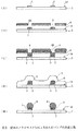
メタルマスク法は、図3(A)に示すように、ウエハ1に形成された各半導体ICの各電極3にそれぞれ対応させて、図3(B)のように開口4Aが設けられたメタルマスク4を用いて行われる。
【0005】
すなわちメタルマスク法では、まずこのメタルマスク4を各開口4Aから半導体ICの対応する電極3及びその周辺部がそれぞれ露出するようにウエハ1の一面1A上に治具(図示せず)を用いて密着させる。
次いでこのメタルマスク4の各開口4Aを介してウエハ1の一面1A上に、例えばスパツタ装置を用いてTi、Cu及びAuなどの金属材をそれぞれ所定の厚みに堆積させることにより各半導体ICの対応する各電極3及びその周辺部上にそれぞれメタルバリア層5を積層形成する。
【0006】
続いて図3(C)に示すように、このバリアメタル層5上に例えば蒸着装置を用いてSn及びPb等のはんだ材を蒸着することによりはんだ層6を形成し、この後ウエハ1の一面1A上からメタルマスク4を除去する。
続いて図3(D)に示すように、各半導体ICの各電極3の周辺部上にそれぞれフラツクス7を塗布し、この後各半導体ICの各電極3上に積層形成された各はんだ層6を加熱溶融した後、ウエハ1の一面1A上に残存するフラツクス7を溶剤を用いて除去する。
【0007】
これによりウエハ1の各半導体ICの各電極3上にそれぞれ図3(E)のような球状のはんだバンプ8を形成することができる。
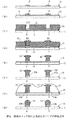
一方電界めつき法においては、例えば図4(A)〜(H)に示すような手順により行われ、まず図4(A)に示すように、ウエハ1の一面1A上に、例えばスパツタリング法などによりTi、Cu又はAuなどの金属材を堆積させることにより図4(B)のようにバリアメタル層10を形成する。
【0008】
次いでこのバリアメタル層10上にフオトレジストを塗布することによりレジスト層11(図4(C))を形成し、この後このレジスト層11を所定パターンで露光し、現像することにより、図4(C)のように各半導体ICの各電極3及びその周辺部と、めつき用取出し電極(図示せず)及びその周辺部とのみがそれぞれ露出するようにレジスト層11をパターニングする。
続いてめつき用取出し電極をアノード側としてめつき浴中ではんだを電解めつきにより堆積させることにより、図4(D)のように所定厚のはんだ層12を形成し、この後図4(E)のように、このウエハ1の一面1A上からレジスト層11を剥離液によつて溶解させることにより除去する。
【0009】
続いて図4(F)に示すように、ウエハ1の一面1A上に形成されたバリアメタル層10のうち、各はんだ層12の直下以外の部分をエツチング液を用いて除去する。
この後ウエハ1の一面1A上に、図4(G)に示すように、各はんだ層12を取り囲むようにフラツクス13をコーテイングした後、これら各はんだ層12を加熱溶融する。これによりウエハ1に形成された各半導体ICの各電極3上にそれぞれ図4(H)に示すような球状のはんだバンプ14を形成することができる。
【0010】
【発明が解決しようとする課題】
ところで、近年、ICの製造技術が飛躍的に進歩し、ウエハ1枚からのICチツプの収量を増加させるために、大口径のウエハを用いることや、ICチツプ内部の配線幅等を縮小させることによるICチツプ自身の小型化、及びそれに伴うICチツプ上の電極の狭ピツチ化が進んでいる。
この場合このようなICチツプの製造工程で用いられるウエハは、一般的に8〃φ以上のものであり、また各ICチツプの電極間隔も 150〔μm〕を切つている。
【0011】
ところが上述したような従来のメタルマスク法では、Mo、Cr又はステンレスなどからなるメタルマスク4と、ウエハ1との間における熱膨張係数の違いから、例えばスパツタリングにより各半導体ICの各電極3上にバリアメタル層5を形成する際や、このバリアメタル層5上に蒸着法によりはんだ層6を形成する際に、発生する熱によつてメタルマスク4の各開口4Aと半導体ICの対応する電極3との間に位置ずれが生じることがあり、このため各半導体ICの各電極3上に精度良くバリアメタル層5やはんだ層6(はんだバンプ8)を形成し難い問題があつた。この傾向はウエハ1が大口径化し、半導体ICの電極ピツチが狭くなる程難しくなる問題があつた。
【0012】
一方上述したような従来のめつき法では、めつき浴中の組成(例えばPb及びSn)の管理が難しく、このため各半導体ICの各電極3上にそれぞれ形成される各はんだバンプ14間に組成のずれが生じたりする問題がある。また従来のめつき法では、めつきによる各はんだ層12の形成時にウエハ1の一面1A全面を均一な電界強度に保つことが難しく、このため各半導体ICの各電極3上にそれぞれ形成されるはんだ層12(及び最終的にこれら各半導体ICの各電極3上にそれぞれ形成されるはんだバンプ14)の高さにばらつきが生じ易い問題がある。このような各はんだバンプ14の組成や高さは、ウエハ1が大口径化する程、制御し難い問題があつた。
【0013】
特にめつき法では、形成される各はんだバンプ14間での高さのばらつきが大きく、このため各電極3上にめつき法を用いてはんだバンプ14が形成されたICチツプを配線基板上にマウントする場合に、1チツプ内におけるはんだバンプ14の高さばらつきのために全てのはんだバンプ14を配線基板上の対応する電極に接合させ難く、実装した半導体ICと配線基板との間で接続不良が生じ易い問題があつた。
【0014】
本発明は以上の点を考慮してなされたもので、大口径のウエハから形成される、狭電極ピツチな各半導体チツプの各電極上に位置精度良く、かつ均一な組成で高さのそろつたバンプを形成することのできる半導体装置の製造方法を提案しようとするものである。
【0015】
【課題を解決するための手段】
かかる課題を解決するため本発明においては、一面に複数の半導体集積回路が形成された半導体ウエハの一面全面上に、フオトレジストからなるレジスト層を形成すると共に当該レジスト層をパターニングすることによりレジスト層に各半導体集積回路の各電極及びその周辺部のみがそれぞれ露出するように複数の開口を形成し、当該レジスト層の各開口をそれぞれ介して半導体ウエハの一面上にバンプ用の金属材を厚みがレジスト層の1.3倍以下となるように蒸着することにより、各半導体集積回路の各電極上にそれぞれ第1のバンプ層を積層形成するとともに、レジスト層上にバンプ用の金属材からなる第2のバンプ層を積層形成し、第1のバンプ層上には貼り付けず、第2のバンプ層上にのみ粘着テープを貼り付けた後、当該粘着テープを引き剥がすことによりレジスト層上から第2のバンプ層を除去し、この後レジスト層を半導体ウエハの一面上から除去した後、第1のバンプ層を加熱溶融して整形するようにして半導体装置を製造するようにした。
【0016】
このように半導体ウエハの一面に積層形成されたレジスト層を各半導体集積回路の各電極が露出するようにパターニングする場合、半導体集積回路の電極ピツチが狭い場合にも各電極にそれぞれ対応させてレジスト層に位置精度良く狭ピツチで開口を形成できる。この開口精度はウエハ径が大きくなつても変化しない。またこのレジスト層の各開口をそれぞれ介して各半導体集積回路の各電極上にバンプ用の金属材を蒸着する場合、当該半導体集積回路の各電極上に均一な組成でかつ高さのばらつきが少なく第1のバンプ層を形成することができる。
【0017】
【発明の実施の形態】
以下図面について、本発明の一実施例を詳述する。
【0018】
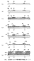
図1(A)〜図2(E)は実施例による半導体装置の製造方法を示すものであり、まずウエハに所定の処理を施すことにより、その一面に複数の半導体ICを形成し(図1(A))、この後ウエハ20の一面20A上に、図1(B)のように各半導体ICの各Al電極22のパツド径を制限しながらポリイミド等からなるパツジベーシヨン膜23を形成する。
【0019】
次いで図1(C)に示すように、このウエハ20の一面20A上に全面に亘つてTi、Cu及びAu等の金属材をスパツタリングすることによりバリアメタル層24を形成する。
この後このバリアメタル層24上にフオトレジストを塗布することによりレジスト層を形成した後、このレジスト層を、露光し、現像することにより、図1(D)のように各半導体ICの各Al電極22及びその周辺部のみが残るようにパターニングする。
【0020】
続いて図1(E)に示すように、ウエハ20の一面20A上に形成されたバリアメタル層24のうち、各半導体ICの各Al電極22及びその周辺部上以外のバリアメタル層24をエツチヤントを用いてエツチングすることにより除去し、この後図1(F)に示すように、残存するバリアメタル層24A上の各レジスト層25をそれぞれ剥離液を用いて除去する。
【0021】
さらにこの後図1(G)に示すように、再びパツシベーシヨン膜23上に高粘度のフオトレジストを塗布することによりレジスト層26を形成すると共に、この後このレジスト層26を露光し、現像するようにしてパターニングすることにより、レジスト層26に各半導体ICの各Al電極22及びその周辺部のみがそれぞれ露出するように複数の開口26Aを形成する。
【0022】
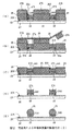
続いてこのレジスト層26の各開口26Aをそれぞれ介してSn及びPb等のはんだ材をウエハ20の一面20A上に蒸着することにより、図2(A)に示すように、各半導体ICの各電極22及びその周辺部上にはんだ層27Aを形成し、この後図2(B)に示すように、上述のはんだ材の蒸着工程(図2(B))時においてレジスト層26上に形成されたはんだ層27B上に粘着テープ30を貼り付けた後、これを引き剥がす。
【0023】
この際粘着テープ30としては、レジスト層26及びはんだ層27B間の密着力よりも粘着力が強いものを用いるようにし、これによりレジスト層26上に形成されたはんだ層27Bを粘着テープ30と一緒に剥ぎ取るようにする。従つてこの工程の終了後、ウエハ20の一面20A上には、図2(C)に示すように、レジスト層26の開口26A内にのみ(すなわち各半導体ICの各電極22上にのみ)はんだ層27Aが残存する。
さらにこの後図2(D)に示すように、ウエハ20の一面20A上からレジスト層26を剥離液を用いて除去する。因に、このような方法により各半導体ICの各Al電極22上に形成されたはんだ層27Aの組成は、蒸着時におけるPb及びSnの蒸気圧の違いにより、上層にSn成分が多くなつている。
【0024】
この後このはんだ層27Aの表面にフラツクスをコーテイングし、当該はんだ層27Aを加熱溶融し、球状に整形した後、フラツクスを洗浄液を使用し除去する。これにより図2(E)に示すように、各半導体ICの各Al電極22上にそれぞれ球形状のはんだバンプ31を形成することができる。
さらにこの後このウエハ20を、各半導体ICをそれぞれ個別に切り離すように分割する。これにより各Al電極22上にそれぞれ球形状のはんだバンプ31が形成されてなるICチツプを得ることができる。
【0025】
ここでこの実施例の場合、はんだ材の蒸着工程(図2(A))では、はんだ層27A、28Bの厚みがレジスト層26の厚みの 1.3倍以下になるようにはんだ層27A、28Bを形成するようにする。
これは実験的に、はんだ層27A、27Bの厚みがレジスト層26の厚みの1.3 倍以上になると、レジスト層26の開口26A内に形成されたはんだ層27Aの一部も粘着テープ30に粘着し、これらが当該粘着テープ30と一緒にウエハ20の一面20A上から剥がれることによりAl電極22上にはんだバンプ31が形成されないおそれがあるためである。
【0026】
従つてはんだ材の蒸着工程(図2(A))において、上述のようにはんだ層27A、27Bの厚みがレジスト層26の厚みの 1.3倍以下となるように制御することにより、このようなはんだバンプ31の欠落を未然に防止することができる。
【0027】
以上の構成において、この実施例では、各半導体ICの各電極22上に形成された各バリアメタル層24A上にはんだ層27Aを形成する工程(図1(G)〜図2(D))を、パツシベーシヨン膜23上にフオトレジストを塗布することによりレジスト層26を形成すると共に、当該レジスト層26を、各半導体ICの各電極22及びその周辺部がそれぞれ露出する開口26Aを有するようにパターニングした後、このレジスト層26をマスクとして各半導体ICの各Al電極22上に形成された各バリアメタル層24A上にはんだを蒸着することにより行う。
【0028】
従つてこの方法では、はんだ材の蒸着工程(図2(A))においてマスクとなるレジスト層26を通常のフオトプロセスを用いてパターニングしている分、各開口26Aを狭いピツチで位置精度良く形成できる。またこの精度はウエハ20の径が大きくなつても変化しないため、ウエハ20が大口径でかつ各半導体ICが狭電極ピツチである場合にもこれら各半導体ICの各電極22にそれぞれ対応させて精度良くはんだ層26の開口26Aを形成することができる。
【0029】
さらにこの方法では、このようにして形成されたレジスト層26の各開口26Aをそれぞれ介して各半導体ICの各電極22上にはんだ層27Aを形成する際に蒸着法を用いるため、これら各電極22上に均一な組成でかつ高さのばらつきが少なくはんだ層27A(及びはんだバンプ31)を形成することができる。
【0030】
従つてこの実施例のような半導体装置の製造方法を用いることによつて、1枚のウエハ20あたりのICチツプの収量を増加させ得ると共に、その分コストも低減させることができ、かつ各半導体ICの各電極22上に高さのばらつきが少なくはんだ層27A(及びはんだバンプ31)を形成し得る分、このICチツプを配線基板に実装する際の当該ICチツプと配線基板との間の接続不良を低減できる。
【0031】
以上の構成によれば、ウエハ20の一面20A上に成膜されたパツシベーシヨン膜23上にフオトレジストを塗布することによりレジスト層26を形成し、当該レジスト層26を露光し、現像することによつて当該レジスト層26に各半導体ICの各電極22にそれぞれ対応させて開口26Aを形成すると共に、このレジトス層26の各開口26Aをそれぞれ介して露出する各半導体ICの各電極22上に蒸着法によりはんだ材を蒸着するようにしてはんだ層27Aを形成するようにしたことにより、ウエハ20の口径に関わりなくレジスト層26の各開口26Aを精度良く形成し得ると共に各半導体ICの各電極22上に均一な組成で高さのばらつきが少なくはんだ層27Aを形成することができ、かくして大口径なウエハから形成される、狭電極ピツチの各半導体ICの各電極上に位置精度良く、かつ均一な組成で高さのそろつたはんだバンプを形成することができる半導体装置の製造方法を実現できる。
【0032】
なお上述の実施例においては、本発明をウエハ20に形成された各半導体ICの各電極22上にはんだバンプ31を形成する際に適用するようにした場合について述べたが、本発明はこれに限らず、各半導体ICの各電極22上にはんだ材以外のバンプ用の金属材からなるバンプを形成する場合にも適用して好適なものである。
【0033】
また上述の実施例においては、レジスト層26上に形成された各はんだ層27Bを除去する際、粘着テープ30を利用するようにした場合について述べたが、本発明はこれに限らず、この他種々の方法を適用できる。この場合はんだ材の蒸着工程(図2(A))では、必要に応じてはんだ層27A、27Bの厚みがレジスト層26の厚みの1.3倍以上となるように制御しても良い。
【0034】
【発明の効果】
上述のように本発明によれば、一面に複数の半導体集積回路が形成された半導体ウエハの一面全面上に、フオトレジストからなるレジスト層を形成すると共に当該レジスト層をパターニングすることによりレジスト層に各半導体集積回路の各電極及びその周辺部のみがそれぞれ露出するように複数の開口を形成し、当該レジスト層の各開口をそれぞれ介して半導体ウエハの一面上にバンプ用の金属材を厚みがレジスト層の1.3倍以下となるように蒸着することにより、各半導体集積回路の各電極上にそれぞれ第1のバンプ層を積層形成するとともに、レジスト層上にバンプ用の金属材からなる第2のバンプ層を積層形成し、第1のバンプ層上には貼り付けず、第2のバンプ層上にのみ粘着テープを貼り付けた後、当該粘着テープを引き剥がすことによりレジスト層上から第2のバンプ層を除去し、この後レジスト層を半導体ウエハの一面上から除去した後、第1のバンプ層を加熱溶融して整形するようにして半導体装置を製造するようにしたことにより、半導体ウエハの口径に関わりなくかつ半導体集積回路の電極ピツチが狭い場合にも各電極にそれぞれ対応させて位置精度良くレジスト層に開口を形成できると共に、このレジスト層の各開口をそれぞれ介して各半導体集積回路の各電極上にバンプ用の金属材を均一な組成でかつ高さのばらつきが少なく供給することができ、かくして大口径なウエハから形成される狭電極ピツチの半導体チツプの各電極上に位置精度良く、かつ均一な組成で高さのそろつたバンプを形成することができる半導体装置の製造方法を実現できる。
【図面の簡単な説明】
【図1】実施例による半導体製造方法に適用するはんだバンプ形成方法の説明に供する断面図である。
【図2】実施例による半導体製造方法に適用するはんだバンプ形成方法の説明に供する断面図である。
【図3】従来のメタルマスク法によるはんだバンプの形成工程を示す断面図である。
【図4】従来のめつき法によるはんだバンプの形成工程を示す断面図である。
【符号の説明】
20……ウエハ、20A、21A……一面、21……半導体IC、22……電極、23……パツシベーシヨン膜、24、24A……バリアメタル層、25、26……レジスト層、27A、27B……はんだ層、30……粘着テープ、31……はんだバンプ。[0001]
【table of contents】
The present invention will be described in the following order.
Technical field to which the invention pertains Conventional technology (FIGS. 3A to 4H)
Problems to be Solved by the Invention (FIGS. 3A to 4H)
Means for Solving the Problems (FIGS. 1A to 2E)
Embodiment of the Invention (FIGS. 1A to 2E)
BACKGROUND OF THE INVENTION
TECHNICAL FIELD OF THE INVENTION
The present invention relates to a method for manufacturing a semiconductor device, and is suitably applicable to, for example, a case where an IC chip having a narrow electrode pitch is formed from a large-diameter semiconductor wafer (hereinafter, a semiconductor wafer is simply referred to as a wafer).
[0003]
[Prior art]
2. Description of the Related Art Conventionally, in an IC chip for mounting a chip such as a flip chip, for example, a plurality of semiconductor integrated circuits are formed by subjecting one surface of a semiconductor single crystal plate called a wafer to predetermined processing such as etching, oxidation and / or impurity implantation in a predetermined pattern. (Semiconductor ICs) are formed, bump electrodes called bumps are formed on the respective electrodes of the respective semiconductor ICs, and then the respective semiconductor ICs are individually cut off.
[0004]
In this case, as a solder bump forming method for forming a solder bump on each electrode of each semiconductor IC before separation, a metal mask method and an electric field plating method have been conventionally used.
In the metal mask method, as shown in FIG. 3A, a metal mask provided with an opening 4A as shown in FIG. 3B corresponding to each
[0005]
That is, in the metal mask method, first, the metal mask 4 is placed on one
Then, a metal material such as Ti, Cu and Au is deposited to a predetermined thickness on one
[0006]
Subsequently, as shown in FIG. 3C, a solder material such as Sn and Pb is vapor-deposited on the
Subsequently, as shown in FIG. 3 (D), a flux 7 is applied on the periphery of each
[0007]
Thereby, the spherical solder bumps 8 as shown in FIG. 3E can be formed on the
On the other hand, in the electric field plating method, for example, it is performed according to a procedure as shown in FIGS. 4A to 4H. First, as shown in FIG. By depositing a metal material such as Ti, Cu or Au, the
[0008]
Next, a photoresist is applied on the
Subsequently, solder is deposited by electrolytic plating in a plating bath with the plating extraction electrode serving as the anode side, thereby forming a
[0009]
Subsequently, as shown in FIG. 4 (F), portions of the
Thereafter, as shown in FIG. 4G, a
[0010]
[Problems to be solved by the invention]
By the way, in recent years, the manufacturing technology of IC has been dramatically advanced, and in order to increase the yield of IC chips from one wafer, it is necessary to use a large-diameter wafer or to reduce the wiring width inside the IC chip. As a result, the size of the IC chip itself is reduced, and the electrodes on the IC chip are made narrower.
In this case, the wafer used in the manufacturing process of such an IC chip generally has a diameter of 8 mm or more, and the interval between the electrodes of each IC chip is less than 150 μm.
[0011]
However, in the conventional metal mask method as described above, due to the difference in the coefficient of thermal expansion between the metal mask 4 made of Mo, Cr, stainless steel or the like and the
[0012]
On the other hand, in the conventional plating method as described above, it is difficult to control the composition (for example, Pb and Sn) in the plating bath, and therefore, between the solder bumps 14 formed on each
[0013]
In particular, in the plating method, there is a large variation in height between the solder bumps 14 to be formed. Therefore, an IC chip having the solder bumps 14 formed on each
[0014]
The present invention has been made in view of the above points, and has a uniform height and a uniform composition on each electrode of each semiconductor chip having a narrow electrode pitch formed from a large-diameter wafer. An object of the present invention is to propose a method of manufacturing a semiconductor device capable of forming a bump.
[0015]
[Means for Solving the Problems]
In order to solve this problem, in the present invention, a resist layer made of a photoresist is formed on the entire surface of a semiconductor wafer having a plurality of semiconductor integrated circuits formed on one surface, and the resist layer is patterned by patterning the resist layer. A plurality of openings are formed so that only the respective electrodes of the respective semiconductor integrated circuits and the peripheral portion thereof are respectively exposed, and a metal material for bumps is formed on one surface of the semiconductor wafer through the respective openings of the resist layer. The first bump layer is formed on each electrode of each semiconductor integrated circuit by vapor deposition so as to be 1.3 times or less of the resist layer, and the second bump made of a metal material for bumps is formed on the resist layer. A bump layer is formed in a laminated form, and an adhesive tape is attached only on the second bump layer without being attached on the first bump layer. The second bump layer is removed from the resist layer by peeling off the resist layer. After that, the resist layer is removed from one surface of the semiconductor wafer. To be manufactured.
[0016]
When the resist layer thus formed on one surface of the semiconductor wafer is patterned so that each electrode of each semiconductor integrated circuit is exposed, even when the electrode pitch of the semiconductor integrated circuit is narrow, the resist is made to correspond to each electrode. An opening can be formed in the layer with a narrow pitch with high positional accuracy. This opening accuracy does not change even when the wafer diameter increases. When a metal material for a bump is deposited on each electrode of each semiconductor integrated circuit through each opening of the resist layer, a uniform composition and little variation in height are formed on each electrode of the semiconductor integrated circuit. A first bump layer can be formed.
[0017]
BEST MODE FOR CARRYING OUT THE INVENTION
An embodiment of the present invention will be described below in detail with reference to the drawings.
[0018]
FIGS. 1A to 2E show a method of manufacturing a semiconductor device according to an embodiment. First, a predetermined process is performed on a wafer to form a plurality of semiconductor ICs on one surface thereof (FIG. 1). (A)) Then, a
[0019]
Next, as shown in FIG. 1C, a
Thereafter, a photoresist layer is formed by applying a photoresist on the
[0020]
Subsequently, as shown in FIG. 1E, among the barrier metal layers 24 formed on one
[0021]
Then, as shown in FIG. 1 (G), a resist
[0022]
Subsequently, a solder material such as Sn and Pb is vapor-deposited on one
[0023]
At this time, as the
Thereafter, as shown in FIG. 2D, the resist
[0024]
Thereafter, a flux is coated on the surface of the
Thereafter, the
[0025]
Here, in the case of this embodiment, in the step of vapor deposition of the solder material (FIG. 2A), the solder layers 27A, 28B are set so that the thickness of the solder layers 27A, 28B is 1.3 times or less the thickness of the resist
When the thickness of the solder layers 27A and 27B becomes 1.3 times or more the thickness of the resist
[0026]
Accordingly, by controlling the thickness of the solder layers 27A and 27B to be equal to or less than 1.3 times the thickness of the resist
[0027]
In the above configuration, in this embodiment, a step of forming a
[0028]
Therefore, in this method, since the resist
[0029]
Further, in this method, the vapor deposition method is used when the
[0030]
Therefore, by using the method of manufacturing a semiconductor device as in this embodiment, the yield of IC chips per one
[0031]
According to the above configuration, the photoresist layer is formed by applying a photoresist on the
[0032]
In the above-described embodiment, the case where the present invention is applied when forming the solder bumps 31 on the
[0033]
Further, in the above-described embodiment, the case where the
[0034]
【The invention's effect】
As described above, according to the present invention, a resist layer made of a photoresist is formed on the entire surface of a semiconductor wafer on which a plurality of semiconductor integrated circuits are formed, and the resist layer is patterned by forming the photoresist layer. A plurality of openings are formed so that only the electrodes of each semiconductor integrated circuit and the peripheral portion thereof are exposed, and a metal material for bumps is formed on one surface of the semiconductor wafer through each opening of the resist layer. The first bump layer is formed on each electrode of each semiconductor integrated circuit by vapor deposition so as to be 1.3 times or less the layer, and the second bump made of a metal material for a bump is formed on the resist layer. After laminating the layers, stick the adhesive tape only on the second bump layer without sticking it on the first bump layer, and peel off the adhesive tape. Removing the second bump layer from the resist layer, and then removing the resist layer from one surface of the semiconductor wafer, and then heating and melting the first bump layer to form a semiconductor device. With this arrangement, regardless of the diameter of the semiconductor wafer and even when the electrode pitch of the semiconductor integrated circuit is narrow, openings can be formed in the resist layer with high positional accuracy corresponding to each electrode, and each opening of the resist layer can be formed. A metal material for a bump can be supplied on each electrode of each semiconductor integrated circuit with a uniform composition and a small variation in height through each of them, and thus a semiconductor chip of a narrow electrode pitch formed from a large-diameter wafer. A method for manufacturing a semiconductor device capable of forming bumps of uniform height and uniform position on each of the electrodes can be realized.
[Brief description of the drawings]
FIG. 1 is a cross-sectional view for explaining a solder bump forming method applied to a semiconductor manufacturing method according to an embodiment.
FIG. 2 is a cross-sectional view for explaining a solder bump forming method applied to the semiconductor manufacturing method according to the embodiment.
FIG. 3 is a cross-sectional view showing a step of forming a solder bump by a conventional metal mask method.
FIG. 4 is a cross-sectional view showing a step of forming a solder bump by a conventional plating method.
[Explanation of symbols]
20
Claims (1)
上記半導体ウエハの上記一面全面上にフオトレジストを塗布することによりレジスト層を積層形成すると共に、当該レジスト層をパターニングすることにより上記レジスト層に各上記半導体集積回路の各電極及びその周辺部のみがそれぞれ露出するように複数の開口を形成する第2の工程と、
上記レジスト層の各上記開口をそれぞれ介して上記半導体ウエハの上記一面上にバンプ用の金属材を厚みが上記レジスト層の1.3倍以下となるように蒸着することにより、各上記半導体集積回路の各上記電極上にそれぞれ第1のバンプ層を積層形成すると共に、上記レジスト層上に上記金属材からなる第2のバンプ層を積層形成する第3の工程と、
上記第1のバンプ層上には貼り付けず、上記第2のバンプ層上にのみ粘着テープを貼り付けた後、当該粘着テープを引き剥がすことにより上記レジスト層上から上記第2のバンプ層を除去する第4の工程と、
上記レジスト層を上記半導体ウエハの上記一面上から除去する第5の工程と、
各上記半導体集積回路の各上記電極上にそれぞれ積層形成された上記第1のバンプ層を加熱溶融して整形する第6の工程と
を具えることを特徴とする半導体装置の製造方法。A first step of forming a plurality of semiconductor integrated circuits on one surface of the semiconductor wafer by performing a predetermined process on the semiconductor wafer;
A resist layer is formed by applying a photoresist over the entire surface of the semiconductor wafer, and only the electrodes of each of the semiconductor integrated circuits and the peripheral portion are formed on the resist layer by patterning the resist layer. a second step that form a plurality of openings to expose respective
By depositing a metal material for bumps on the one surface of the semiconductor wafer through each of the openings of the resist layer so that the thickness is 1.3 times or less of the resist layer, each of the semiconductor integrated circuits is A third step of laminating and forming a first bump layer on each of the electrodes, and laminating and forming a second bump layer made of the metal material on the resist layer;
After sticking an adhesive tape only on the second bump layer without sticking on the first bump layer, the adhesive tape is peeled off to remove the second bump layer from the resist layer. A fourth step of removing;
A fifth step of removing the resist layer from the one surface of the semiconductor wafer;
A sixth step of heating and melting the first bump layer laminated on each of the electrodes of each of the semiconductor integrated circuits to shape the first bump layer.
Priority Applications (1)
| Application Number | Priority Date | Filing Date | Title |
|---|---|---|---|
| JP26072895A JP3580452B2 (en) | 1995-09-12 | 1995-09-12 | Method for manufacturing semiconductor device |
Applications Claiming Priority (1)
| Application Number | Priority Date | Filing Date | Title |
|---|---|---|---|
| JP26072895A JP3580452B2 (en) | 1995-09-12 | 1995-09-12 | Method for manufacturing semiconductor device |
Publications (2)
| Publication Number | Publication Date |
|---|---|
| JPH0982717A JPH0982717A (en) | 1997-03-28 |
| JP3580452B2 true JP3580452B2 (en) | 2004-10-20 |
Family
ID=17351934
Family Applications (1)
| Application Number | Title | Priority Date | Filing Date |
|---|---|---|---|
| JP26072895A Expired - Fee Related JP3580452B2 (en) | 1995-09-12 | 1995-09-12 | Method for manufacturing semiconductor device |
Country Status (1)
| Country | Link |
|---|---|
| JP (1) | JP3580452B2 (en) |
-
1995
- 1995-09-12 JP JP26072895A patent/JP3580452B2/en not_active Expired - Fee Related
Also Published As
| Publication number | Publication date |
|---|---|
| JPH0982717A (en) | 1997-03-28 |
Similar Documents
| Publication | Publication Date | Title |
|---|---|---|
| EP1032030B1 (en) | Flip chip bump bonding | |
| US5376584A (en) | Process of making pad structure for solder ball limiting metallurgy having reduced edge stress | |
| US6461953B1 (en) | Solder bump forming method, electronic component mounting method, and electronic component mounting structure | |
| US20060279000A1 (en) | Pre-solder structure on semiconductor package substrate and method for fabricating the same | |
| KR100510543B1 (en) | Method for forming bump without surface defect | |
| WO1996030933A2 (en) | Solder bump fabrication methods and structure including a titanium barrier layer | |
| JPH09199506A (en) | Bump forming method for semiconductor element | |
| JP2643097B2 (en) | Metal contact formation method | |
| JP3267167B2 (en) | Semiconductor device and manufacturing method thereof | |
| JP3580452B2 (en) | Method for manufacturing semiconductor device | |
| JPH0945691A (en) | Solder bump for chip component and manufacturing method thereof | |
| JP2811741B2 (en) | Method for manufacturing semiconductor device | |
| KR0165883B1 (en) | Gold / Tin Process Bonding for Tape Automated Bonding Process | |
| JPH03198342A (en) | Manufacture of semiconductor device | |
| US20060128134A1 (en) | Method for re-routing lithography-free microelectronic devices | |
| JPH09306918A (en) | Barrier metal forming method in solder ball bump forming process | |
| JP3362574B2 (en) | Method of forming barrier metal | |
| JPH02271635A (en) | Manufacture of semiconductor device | |
| JPH0510365Y2 (en) | ||
| JPH02232947A (en) | Semiconductor integrated circuit device and mounting thereof | |
| JPH0437139A (en) | Formation of metal protruding electrode | |
| JPH05243232A (en) | Method for forming solder bump electrodes | |
| JP2978973B2 (en) | Solder bump formation method | |
| JP2600669B2 (en) | Metal bump for transfer bump | |
| JP3036300B2 (en) | Method for manufacturing TAB tape and method for manufacturing semiconductor device |
Legal Events
| Date | Code | Title | Description |
|---|---|---|---|
| A521 | Request for written amendment filed |
Free format text: JAPANESE INTERMEDIATE CODE: A523 Effective date: 20031225 |
|
| A02 | Decision of refusal |
Free format text: JAPANESE INTERMEDIATE CODE: A02 Effective date: 20040123 |
|
| A521 | Request for written amendment filed |
Free format text: JAPANESE INTERMEDIATE CODE: A523 Effective date: 20040324 |
|
| A521 | Request for written amendment filed |
Free format text: JAPANESE INTERMEDIATE CODE: A523 Effective date: 20040510 |
|
| A911 | Transfer to examiner for re-examination before appeal (zenchi) |
Free format text: JAPANESE INTERMEDIATE CODE: A911 Effective date: 20040513 |
|
| A131 | Notification of reasons for refusal |
Free format text: JAPANESE INTERMEDIATE CODE: A131 Effective date: 20040604 |
|
| A521 | Request for written amendment filed |
Free format text: JAPANESE INTERMEDIATE CODE: A523 Effective date: 20040614 |
|
| TRDD | Decision of grant or rejection written | ||
| A01 | Written decision to grant a patent or to grant a registration (utility model) |
Free format text: JAPANESE INTERMEDIATE CODE: A01 Effective date: 20040702 |
|
| A61 | First payment of annual fees (during grant procedure) |
Free format text: JAPANESE INTERMEDIATE CODE: A61 Effective date: 20040715 |
|
| FPAY | Renewal fee payment (event date is renewal date of database) |
Free format text: PAYMENT UNTIL: 20080730 Year of fee payment: 4 |
|
| FPAY | Renewal fee payment (event date is renewal date of database) |
Free format text: PAYMENT UNTIL: 20090730 Year of fee payment: 5 |
|
| LAPS | Cancellation because of no payment of annual fees |