JP2022017531A - ひずみゲージ - Google Patents
ひずみゲージ Download PDFInfo
- Publication number
- JP2022017531A JP2022017531A JP2021182373A JP2021182373A JP2022017531A JP 2022017531 A JP2022017531 A JP 2022017531A JP 2021182373 A JP2021182373 A JP 2021182373A JP 2021182373 A JP2021182373 A JP 2021182373A JP 2022017531 A JP2022017531 A JP 2022017531A
- Authority
- JP
- Japan
- Prior art keywords
- resistor
- strain gauge
- resistance value
- base material
- hole
- Prior art date
- Legal status (The legal status is an assumption and is not a legal conclusion. Google has not performed a legal analysis and makes no representation as to the accuracy of the status listed.)
- Granted
Links
Images


Landscapes
- Measurement Of Length, Angles, Or The Like Using Electric Or Magnetic Means (AREA)
- Laminated Bodies (AREA)
Abstract
【解決手段】本ひずみゲージ1は、可撓性を有する基材10と、基材10上に、クロムとニッケルの少なくとも一方を含む材料から形成された抵抗体30と、を有し、抵抗体30には、複数の貫通孔30xが配列され、貫通孔30xは基材10を貫通しない。
【選択図】図2
Description
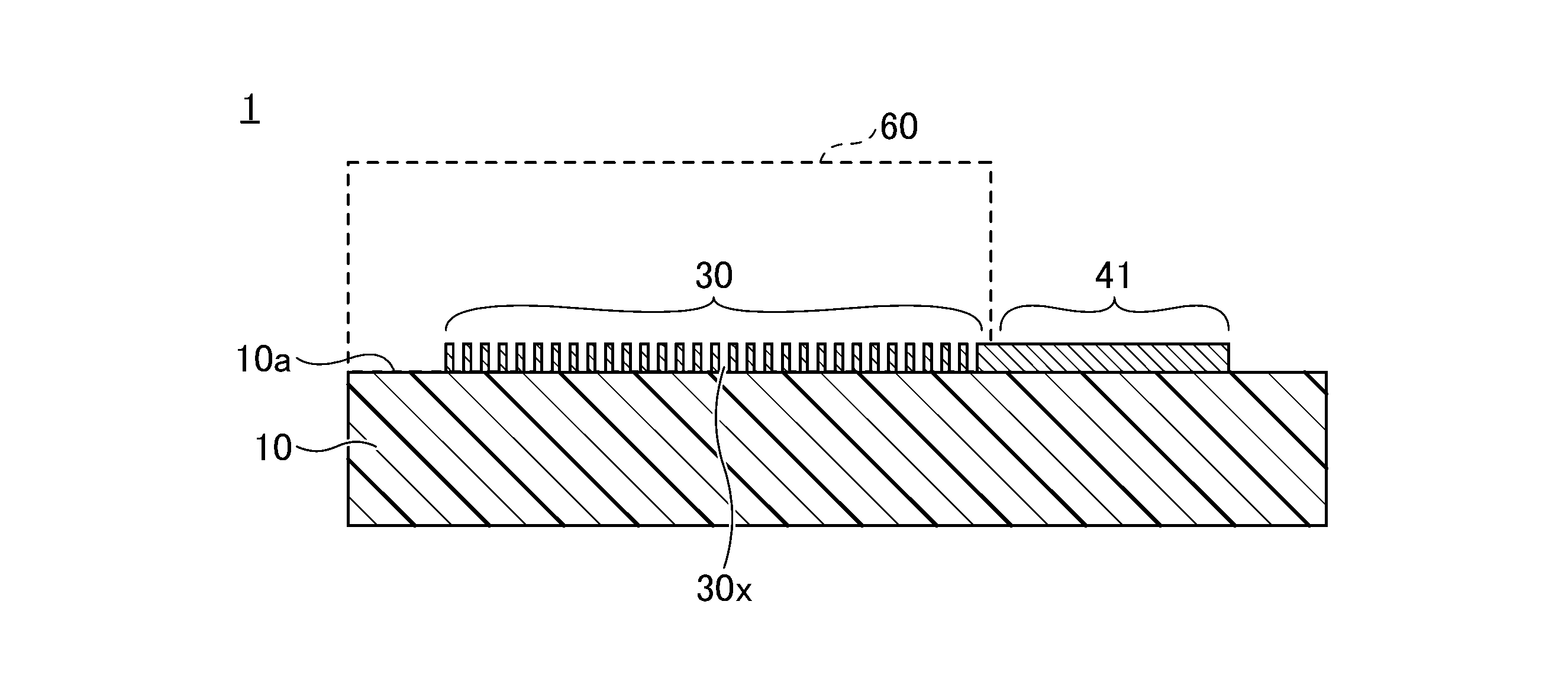
図1は、第1の実施の形態に係るひずみゲージを例示する平面図である。図2は、第1の実施の形態に係るひずみゲージを例示する断面図であり、図1のA-A線に沿う断面を示している。図1及び図2を参照するに、ひずみゲージ1は、基材10と、抵抗体30と、端子部41とを有している。


第1の実施の形態の変形例1では、抵抗値調整領域を備えたひずみゲージの例を示す。なお、第1の実施の形態の変形例1において、既に説明した実施の形態と同一構成部についての説明は省略する場合がある。
なお、予め形成されている貫通孔30xと、抵抗値の調整時に抵抗値調整領域35に形成する貫通孔とは、大きさ及び/又は密度(配置間隔)が異なっていてもよい。例えば、図6(d)に示すように、平面形状が円形の貫通孔30yを形成してもよい。又、抵抗値調整領域35は、必ずしも抵抗体30の端部に配置する必要はなく、抵抗体30の任意の位置に配置することができる。又、抵抗体30のパターンに複数個の抵抗値調整領域35を画定しても構わない。
Claims (9)
- 可撓性を有する基材と、
前記基材上に、クロムとニッケルの少なくとも一方を含む材料から形成された抵抗体と、を有し、
前記抵抗体には、複数の貫通孔が配列され、前記貫通孔は前記基材を貫通しないひずみゲージ。 - 前記貫通孔の平面形状は正方形又は長方形である請求項1に記載のひずみゲージ。
- 前記抵抗体は、アルファクロムを主成分とする請求項1又は2に記載のひずみゲージ。
- 前記抵抗体は、アルファクロムを80重量%以上含む請求項3に記載のひずみゲージ。
- 前記抵抗体は、窒化クロムを含む請求項3又は4に記載のひずみゲージ。
- 前記基材の一方の面に、金属、合金、又は、金属の化合物から形成された機能層を有し、
前記抵抗体は、前記機能層の一方の面に形成されている請求項1乃至5の何れか一項に記載のひずみゲージ。 - 前記機能層は、前記抵抗体の結晶成長を促進する機能を有する請求項6に記載のひずみゲージ。
- 前記抵抗体を被覆する絶縁樹脂層を有する請求項1乃至7の何れか一項に記載のひずみゲージ。
- 可撓性を有する基材と、
前記基材上に、クロムとニッケルの少なくとも一方を含む材料から形成された抵抗体と、を有し、
前記抵抗体には、複数の貫通孔が配列され、
前記貫通孔の平面形状は正方形又は長方形であるひずみゲージ。
Priority Applications (1)
| Application Number | Priority Date | Filing Date | Title |
|---|---|---|---|
| JP2021182373A JP7350037B2 (ja) | 2017-10-17 | 2021-11-09 | ひずみゲージ |
Applications Claiming Priority (2)
| Application Number | Priority Date | Filing Date | Title |
|---|---|---|---|
| JP2017201065A JP7053215B2 (ja) | 2017-10-17 | 2017-10-17 | ひずみゲージ |
| JP2021182373A JP7350037B2 (ja) | 2017-10-17 | 2021-11-09 | ひずみゲージ |
Related Parent Applications (1)
| Application Number | Title | Priority Date | Filing Date |
|---|---|---|---|
| JP2017201065A Division JP7053215B2 (ja) | 2017-10-17 | 2017-10-17 | ひずみゲージ |
Publications (2)
| Publication Number | Publication Date |
|---|---|
| JP2022017531A true JP2022017531A (ja) | 2022-01-25 |
| JP7350037B2 JP7350037B2 (ja) | 2023-09-25 |
Family
ID=66544046
Family Applications (2)
| Application Number | Title | Priority Date | Filing Date |
|---|---|---|---|
| JP2017201065A Active JP7053215B2 (ja) | 2017-10-17 | 2017-10-17 | ひずみゲージ |
| JP2021182373A Active JP7350037B2 (ja) | 2017-10-17 | 2021-11-09 | ひずみゲージ |
Family Applications Before (1)
| Application Number | Title | Priority Date | Filing Date |
|---|---|---|---|
| JP2017201065A Active JP7053215B2 (ja) | 2017-10-17 | 2017-10-17 | ひずみゲージ |
Country Status (1)
| Country | Link |
|---|---|
| JP (2) | JP7053215B2 (ja) |
Families Citing this family (2)
| Publication number | Priority date | Publication date | Assignee | Title |
|---|---|---|---|---|
| JP7737790B2 (ja) * | 2020-10-16 | 2025-09-11 | ミネベアミツミ株式会社 | ひずみゲージ |
| JP7577908B2 (ja) * | 2020-11-06 | 2024-11-06 | ミネベアミツミ株式会社 | ひずみゲージ |
Citations (3)
| Publication number | Priority date | Publication date | Assignee | Title |
|---|---|---|---|---|
| JPS5344052A (en) * | 1976-09-15 | 1978-04-20 | Gen Electric | Thin film strain meter and method of producing same |
| JPS57196124A (en) * | 1981-05-27 | 1982-12-02 | Toshiba Corp | Load cell |
| JPH06300649A (ja) * | 1993-04-12 | 1994-10-28 | Sumitomo Electric Ind Ltd | 薄膜歪抵抗材料とその製造方法及び薄膜歪みセンサ |
Family Cites Families (3)
| Publication number | Priority date | Publication date | Assignee | Title |
|---|---|---|---|---|
| JP6084393B2 (ja) * | 2012-08-08 | 2017-02-22 | 公益財団法人電磁材料研究所 | 歪センサおよび歪の測定方法 |
| JP6159613B2 (ja) * | 2013-08-05 | 2017-07-05 | 公益財団法人電磁材料研究所 | 歪センサ |
| JP2016011937A (ja) * | 2014-06-30 | 2016-01-21 | 新日鉄住金化学株式会社 | ひずみゲージ及びその材料 |
-
2017
- 2017-10-17 JP JP2017201065A patent/JP7053215B2/ja active Active
-
2021
- 2021-11-09 JP JP2021182373A patent/JP7350037B2/ja active Active
Patent Citations (3)
| Publication number | Priority date | Publication date | Assignee | Title |
|---|---|---|---|---|
| JPS5344052A (en) * | 1976-09-15 | 1978-04-20 | Gen Electric | Thin film strain meter and method of producing same |
| JPS57196124A (en) * | 1981-05-27 | 1982-12-02 | Toshiba Corp | Load cell |
| JPH06300649A (ja) * | 1993-04-12 | 1994-10-28 | Sumitomo Electric Ind Ltd | 薄膜歪抵抗材料とその製造方法及び薄膜歪みセンサ |
Also Published As
| Publication number | Publication date |
|---|---|
| JP2019074420A (ja) | 2019-05-16 |
| JP7350037B2 (ja) | 2023-09-25 |
| JP7053215B2 (ja) | 2022-04-12 |
Similar Documents
| Publication | Publication Date | Title |
|---|---|---|
| JP7764650B2 (ja) | ひずみゲージ | |
| JP6793103B2 (ja) | ひずみゲージ | |
| JP2025074251A (ja) | ひずみゲージ | |
| JP2023087025A (ja) | ひずみゲージ | |
| US11796404B2 (en) | Strain gauge | |
| JP2025120476A (ja) | ひずみゲージ | |
| JP2025128352A (ja) | ひずみゲージ | |
| JP2023126667A (ja) | ひずみゲージ | |
| JP2025074254A (ja) | ひずみゲージ | |
| WO2019194145A1 (ja) | ひずみゲージ及びその製造方法 | |
| JP2025166170A (ja) | ひずみゲージ | |
| JP2023087026A (ja) | ひずみゲージ | |
| JP2023107861A (ja) | ひずみゲージ | |
| JP7021922B2 (ja) | ひずみゲージ | |
| JP2022017531A (ja) | ひずみゲージ | |
| JP7021912B2 (ja) | ひずみゲージ | |
| WO2021193405A1 (ja) | ひずみゲージ | |
| JP2020129013A (ja) | ひずみゲージ | |
| JP2021110703A (ja) | ひずみゲージ | |
| JP2021156815A (ja) | ひずみゲージ | |
| JP7211807B2 (ja) | ひずみゲージ | |
| JP2019219313A (ja) | センサモジュール | |
| JP2022022448A (ja) | ひずみゲージ | |
| JP2021162401A (ja) | ひずみゲージ | |
| JP2025115513A (ja) | ひずみゲージ |
Legal Events
| Date | Code | Title | Description |
|---|---|---|---|
| A621 | Written request for application examination |
Free format text: JAPANESE INTERMEDIATE CODE: A621 Effective date: 20211207 |
|
| A977 | Report on retrieval |
Free format text: JAPANESE INTERMEDIATE CODE: A971007 Effective date: 20221129 |
|
| A131 | Notification of reasons for refusal |
Free format text: JAPANESE INTERMEDIATE CODE: A131 Effective date: 20221206 |
|
| A521 | Request for written amendment filed |
Free format text: JAPANESE INTERMEDIATE CODE: A523 Effective date: 20230130 |
|
| A02 | Decision of refusal |
Free format text: JAPANESE INTERMEDIATE CODE: A02 Effective date: 20230425 |
|
| A521 | Request for written amendment filed |
Free format text: JAPANESE INTERMEDIATE CODE: A523 Effective date: 20230724 |
|
| A911 | Transfer to examiner for re-examination before appeal (zenchi) |
Free format text: JAPANESE INTERMEDIATE CODE: A911 Effective date: 20230802 |
|
| TRDD | Decision of grant or rejection written | ||
| A01 | Written decision to grant a patent or to grant a registration (utility model) |
Free format text: JAPANESE INTERMEDIATE CODE: A01 Effective date: 20230905 |
|
| A61 | First payment of annual fees (during grant procedure) |
Free format text: JAPANESE INTERMEDIATE CODE: A61 Effective date: 20230912 |
|
| R150 | Certificate of patent or registration of utility model |
Ref document number: 7350037 Country of ref document: JP Free format text: JAPANESE INTERMEDIATE CODE: R150 |