JP2020529729A - ナノポーラスマイクロledデバイスおよび製造方法 - Google Patents
ナノポーラスマイクロledデバイスおよび製造方法 Download PDFInfo
- Publication number
- JP2020529729A JP2020529729A JP2020505177A JP2020505177A JP2020529729A JP 2020529729 A JP2020529729 A JP 2020529729A JP 2020505177 A JP2020505177 A JP 2020505177A JP 2020505177 A JP2020505177 A JP 2020505177A JP 2020529729 A JP2020529729 A JP 2020529729A
- Authority
- JP
- Japan
- Prior art keywords
- gan
- layer
- led device
- diode
- diodes
- Prior art date
- Legal status (The legal status is an assumption and is not a legal conclusion. Google has not performed a legal analysis and makes no representation as to the accuracy of the status listed.)
- Pending
Links
Images


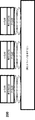


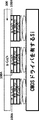
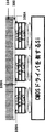


Classifications
-
- H—ELECTRICITY
- H10—SEMICONDUCTOR DEVICES; ELECTRIC SOLID-STATE DEVICES NOT OTHERWISE PROVIDED FOR
- H10H—INORGANIC LIGHT-EMITTING SEMICONDUCTOR DEVICES HAVING POTENTIAL BARRIERS
- H10H20/00—Individual inorganic light-emitting semiconductor devices having potential barriers, e.g. light-emitting diodes [LED]
- H10H20/80—Constructional details
- H10H20/85—Packages
- H10H20/851—Wavelength conversion means
- H10H20/8514—Wavelength conversion means characterised by their shape, e.g. plate or foil
-
- C—CHEMISTRY; METALLURGY
- C09—DYES; PAINTS; POLISHES; NATURAL RESINS; ADHESIVES; COMPOSITIONS NOT OTHERWISE PROVIDED FOR; APPLICATIONS OF MATERIALS NOT OTHERWISE PROVIDED FOR
- C09K—MATERIALS FOR MISCELLANEOUS APPLICATIONS, NOT PROVIDED FOR ELSEWHERE
- C09K11/00—Luminescent materials, e.g. electroluminescent or chemiluminescent
- C09K11/08—Luminescent materials, e.g. electroluminescent or chemiluminescent containing inorganic luminescent materials
- C09K11/88—Luminescent materials, e.g. electroluminescent or chemiluminescent containing inorganic luminescent materials containing selenium, tellurium or unspecified chalcogen elements
- C09K11/881—Chalcogenides
- C09K11/883—Chalcogenides with zinc or cadmium
-
- H—ELECTRICITY
- H10—SEMICONDUCTOR DEVICES; ELECTRIC SOLID-STATE DEVICES NOT OTHERWISE PROVIDED FOR
- H10H—INORGANIC LIGHT-EMITTING SEMICONDUCTOR DEVICES HAVING POTENTIAL BARRIERS
- H10H20/00—Individual inorganic light-emitting semiconductor devices having potential barriers, e.g. light-emitting diodes [LED]
- H10H20/80—Constructional details
- H10H20/81—Bodies
- H10H20/811—Bodies having quantum effect structures or superlattices, e.g. tunnel junctions
- H10H20/812—Bodies having quantum effect structures or superlattices, e.g. tunnel junctions within the light-emitting regions, e.g. having quantum confinement structures
-
- H—ELECTRICITY
- H10—SEMICONDUCTOR DEVICES; ELECTRIC SOLID-STATE DEVICES NOT OTHERWISE PROVIDED FOR
- H10H—INORGANIC LIGHT-EMITTING SEMICONDUCTOR DEVICES HAVING POTENTIAL BARRIERS
- H10H20/00—Individual inorganic light-emitting semiconductor devices having potential barriers, e.g. light-emitting diodes [LED]
- H10H20/80—Constructional details
- H10H20/81—Bodies
- H10H20/817—Bodies characterised by the crystal structures or orientations, e.g. polycrystalline, amorphous or porous
-
- H—ELECTRICITY
- H10—SEMICONDUCTOR DEVICES; ELECTRIC SOLID-STATE DEVICES NOT OTHERWISE PROVIDED FOR
- H10H—INORGANIC LIGHT-EMITTING SEMICONDUCTOR DEVICES HAVING POTENTIAL BARRIERS
- H10H20/00—Individual inorganic light-emitting semiconductor devices having potential barriers, e.g. light-emitting diodes [LED]
- H10H20/80—Constructional details
- H10H20/81—Bodies
- H10H20/819—Bodies characterised by their shape, e.g. curved or truncated substrates
- H10H20/82—Roughened surfaces, e.g. at the interface between epitaxial layers
-
- H—ELECTRICITY
- H10—SEMICONDUCTOR DEVICES; ELECTRIC SOLID-STATE DEVICES NOT OTHERWISE PROVIDED FOR
- H10H—INORGANIC LIGHT-EMITTING SEMICONDUCTOR DEVICES HAVING POTENTIAL BARRIERS
- H10H20/00—Individual inorganic light-emitting semiconductor devices having potential barriers, e.g. light-emitting diodes [LED]
- H10H20/80—Constructional details
- H10H20/81—Bodies
- H10H20/822—Materials of the light-emitting regions
- H10H20/824—Materials of the light-emitting regions comprising only Group III-V materials, e.g. GaP
- H10H20/825—Materials of the light-emitting regions comprising only Group III-V materials, e.g. GaP containing nitrogen, e.g. GaN
-
- H—ELECTRICITY
- H10—SEMICONDUCTOR DEVICES; ELECTRIC SOLID-STATE DEVICES NOT OTHERWISE PROVIDED FOR
- H10H—INORGANIC LIGHT-EMITTING SEMICONDUCTOR DEVICES HAVING POTENTIAL BARRIERS
- H10H20/00—Individual inorganic light-emitting semiconductor devices having potential barriers, e.g. light-emitting diodes [LED]
- H10H20/80—Constructional details
- H10H20/83—Electrodes
- H10H20/832—Electrodes characterised by their material
- H10H20/833—Transparent materials
-
- H—ELECTRICITY
- H10—SEMICONDUCTOR DEVICES; ELECTRIC SOLID-STATE DEVICES NOT OTHERWISE PROVIDED FOR
- H10H—INORGANIC LIGHT-EMITTING SEMICONDUCTOR DEVICES HAVING POTENTIAL BARRIERS
- H10H20/00—Individual inorganic light-emitting semiconductor devices having potential barriers, e.g. light-emitting diodes [LED]
- H10H20/80—Constructional details
- H10H20/85—Packages
- H10H20/851—Wavelength conversion means
- H10H20/8511—Wavelength conversion means characterised by their material, e.g. binder
- H10H20/8512—Wavelength conversion materials
-
- H—ELECTRICITY
- H10—SEMICONDUCTOR DEVICES; ELECTRIC SOLID-STATE DEVICES NOT OTHERWISE PROVIDED FOR
- H10H—INORGANIC LIGHT-EMITTING SEMICONDUCTOR DEVICES HAVING POTENTIAL BARRIERS
- H10H20/00—Individual inorganic light-emitting semiconductor devices having potential barriers, e.g. light-emitting diodes [LED]
- H10H20/80—Constructional details
- H10H20/85—Packages
- H10H20/857—Interconnections, e.g. lead-frames, bond wires or solder balls
-
- H—ELECTRICITY
- H10—SEMICONDUCTOR DEVICES; ELECTRIC SOLID-STATE DEVICES NOT OTHERWISE PROVIDED FOR
- H10W—GENERIC PACKAGES, INTERCONNECTIONS, CONNECTORS OR OTHER CONSTRUCTIONAL DETAILS OF DEVICES COVERED BY CLASS H10
- H10W90/00—Package configurations
-
- B—PERFORMING OPERATIONS; TRANSPORTING
- B82—NANOTECHNOLOGY
- B82Y—SPECIFIC USES OR APPLICATIONS OF NANOSTRUCTURES; MEASUREMENT OR ANALYSIS OF NANOSTRUCTURES; MANUFACTURE OR TREATMENT OF NANOSTRUCTURES
- B82Y20/00—Nanooptics, e.g. quantum optics or photonic crystals
-
- B—PERFORMING OPERATIONS; TRANSPORTING
- B82—NANOTECHNOLOGY
- B82Y—SPECIFIC USES OR APPLICATIONS OF NANOSTRUCTURES; MEASUREMENT OR ANALYSIS OF NANOSTRUCTURES; MANUFACTURE OR TREATMENT OF NANOSTRUCTURES
- B82Y40/00—Manufacture or treatment of nanostructures
-
- H—ELECTRICITY
- H10—SEMICONDUCTOR DEVICES; ELECTRIC SOLID-STATE DEVICES NOT OTHERWISE PROVIDED FOR
- H10H—INORGANIC LIGHT-EMITTING SEMICONDUCTOR DEVICES HAVING POTENTIAL BARRIERS
- H10H20/00—Individual inorganic light-emitting semiconductor devices having potential barriers, e.g. light-emitting diodes [LED]
- H10H20/01—Manufacture or treatment
- H10H20/036—Manufacture or treatment of packages
-
- H—ELECTRICITY
- H10—SEMICONDUCTOR DEVICES; ELECTRIC SOLID-STATE DEVICES NOT OTHERWISE PROVIDED FOR
- H10H—INORGANIC LIGHT-EMITTING SEMICONDUCTOR DEVICES HAVING POTENTIAL BARRIERS
- H10H20/00—Individual inorganic light-emitting semiconductor devices having potential barriers, e.g. light-emitting diodes [LED]
- H10H20/01—Manufacture or treatment
- H10H20/036—Manufacture or treatment of packages
- H10H20/0361—Manufacture or treatment of packages of wavelength conversion means
-
- H—ELECTRICITY
- H10—SEMICONDUCTOR DEVICES; ELECTRIC SOLID-STATE DEVICES NOT OTHERWISE PROVIDED FOR
- H10H—INORGANIC LIGHT-EMITTING SEMICONDUCTOR DEVICES HAVING POTENTIAL BARRIERS
- H10H20/00—Individual inorganic light-emitting semiconductor devices having potential barriers, e.g. light-emitting diodes [LED]
- H10H20/01—Manufacture or treatment
- H10H20/036—Manufacture or treatment of packages
- H10H20/0364—Manufacture or treatment of packages of interconnections
-
- H—ELECTRICITY
- H10—SEMICONDUCTOR DEVICES; ELECTRIC SOLID-STATE DEVICES NOT OTHERWISE PROVIDED FOR
- H10H—INORGANIC LIGHT-EMITTING SEMICONDUCTOR DEVICES HAVING POTENTIAL BARRIERS
- H10H20/00—Individual inorganic light-emitting semiconductor devices having potential barriers, e.g. light-emitting diodes [LED]
- H10H20/80—Constructional details
- H10H20/85—Packages
- H10H20/851—Wavelength conversion means
- H10H20/8511—Wavelength conversion means characterised by their material, e.g. binder
- H10H20/8512—Wavelength conversion materials
- H10H20/8513—Wavelength conversion materials having two or more wavelength conversion materials
-
- H—ELECTRICITY
- H10—SEMICONDUCTOR DEVICES; ELECTRIC SOLID-STATE DEVICES NOT OTHERWISE PROVIDED FOR
- H10H—INORGANIC LIGHT-EMITTING SEMICONDUCTOR DEVICES HAVING POTENTIAL BARRIERS
- H10H29/00—Integrated devices, or assemblies of multiple devices, comprising at least one light-emitting semiconductor element covered by group H10H20/00
- H10H29/10—Integrated devices comprising at least one light-emitting semiconductor component covered by group H10H20/00
- H10H29/14—Integrated devices comprising at least one light-emitting semiconductor component covered by group H10H20/00 comprising multiple light-emitting semiconductor components
- H10H29/142—Two-dimensional arrangements, e.g. asymmetric LED layout
Landscapes
- Chemical & Material Sciences (AREA)
- Inorganic Chemistry (AREA)
- Engineering & Computer Science (AREA)
- Materials Engineering (AREA)
- Organic Chemistry (AREA)
- Led Devices (AREA)
- Led Device Packages (AREA)
Applications Claiming Priority (3)
| Application Number | Priority Date | Filing Date | Title |
|---|---|---|---|
| US201762538994P | 2017-07-31 | 2017-07-31 | |
| US62/538,994 | 2017-07-31 | ||
| PCT/US2018/044023 WO2019027820A1 (en) | 2017-07-31 | 2018-07-27 | MICRO-LED NANOPOROUS DEVICES AND METHODS OF MAKING SAME |
Publications (2)
| Publication Number | Publication Date |
|---|---|
| JP2020529729A true JP2020529729A (ja) | 2020-10-08 |
| JP2020529729A5 JP2020529729A5 (cg-RX-API-DMAC7.html) | 2022-11-16 |
Family
ID=65234177
Family Applications (1)
| Application Number | Title | Priority Date | Filing Date |
|---|---|---|---|
| JP2020505177A Pending JP2020529729A (ja) | 2017-07-31 | 2018-07-27 | ナノポーラスマイクロledデバイスおよび製造方法 |
Country Status (5)
| Country | Link |
|---|---|
| US (1) | US20200152841A1 (cg-RX-API-DMAC7.html) |
| EP (1) | EP3662518A4 (cg-RX-API-DMAC7.html) |
| JP (1) | JP2020529729A (cg-RX-API-DMAC7.html) |
| CN (1) | CN111052418A (cg-RX-API-DMAC7.html) |
| WO (1) | WO2019027820A1 (cg-RX-API-DMAC7.html) |
Cited By (8)
| Publication number | Priority date | Publication date | Assignee | Title |
|---|---|---|---|---|
| JP2022527622A (ja) * | 2020-03-03 | 2022-06-02 | 東莞市中麒光電技術有限公司 | 発光ダイオード及びその製造方法 |
| KR20220139242A (ko) * | 2021-04-07 | 2022-10-14 | 삼성전자주식회사 | 칼라 변환 구조물, 디스플레이 장치 및 디스플레이 장치 제조 방법 |
| JP2022550015A (ja) * | 2019-09-27 | 2022-11-30 | ニュー シリコン コーポレーション プライベート リミテッド | 半導体デバイスを製造する方法およびその半導体デバイス |
| KR20230082436A (ko) * | 2021-12-01 | 2023-06-08 | 삼성전자주식회사 | 마이크로 발광 반도체 소자, 이를 포함한 디스플레이 장치 및 그 제조 방법 |
| KR20230092393A (ko) * | 2021-12-17 | 2023-06-26 | 삼성전자주식회사 | 색 변환 필름, 디스플레이 장치 및 색 변환 필름 제조 방법 |
| US12170344B2 (en) | 2021-04-30 | 2024-12-17 | Samsung Display Co., Ltd. | Display device including partitioning wall comprising transparent conductive oxide and method for manufacturing the same |
| US12272768B2 (en) | 2021-04-30 | 2025-04-08 | Samsung Display Co., Ltd. | Display device and method for fabricating the same |
| US12402464B2 (en) | 2021-04-30 | 2025-08-26 | Samsung Display Co., Ltd. | Display device and method of manufacturing the same |
Families Citing this family (37)
| Publication number | Priority date | Publication date | Assignee | Title |
|---|---|---|---|---|
| CN110212064B (zh) * | 2018-02-28 | 2020-10-09 | 华为技术有限公司 | 一种发光二极管芯片及其制备方法 |
| US11870015B2 (en) | 2019-03-11 | 2024-01-09 | Saphlux, Inc. | Light conversion devices incorporating quantum dots |
| US11757072B2 (en) * | 2019-03-11 | 2023-09-12 | Saphlux, Inc. | Semiconductor devices incorporating quantum dots |
| CN110058412B (zh) * | 2019-04-23 | 2020-02-18 | 深圳惠牛科技有限公司 | 一种传输解耦的大视场光波导镜片 |
| US11094530B2 (en) | 2019-05-14 | 2021-08-17 | Applied Materials, Inc. | In-situ curing of color conversion layer |
| US11239213B2 (en) * | 2019-05-17 | 2022-02-01 | Applied Materials, Inc. | In-situ curing of color conversion layer in recess |
| CN110992841A (zh) * | 2019-11-06 | 2020-04-10 | 深圳市华星光电半导体显示技术有限公司 | 显示装置及显示装置的制作方法 |
| FR3105567B1 (fr) * | 2019-12-19 | 2021-12-17 | Commissariat Energie Atomique | Procede pour fabriquer une structure gan/ingan relaxee |
| JP7812332B2 (ja) * | 2020-01-21 | 2026-02-09 | サフラックス エルエルシー | 量子ドットを組み込んだ半導体デバイス |
| US12593537B2 (en) | 2020-01-22 | 2026-03-31 | Poro Technologies Ltd | Semiconductor structure and method of manufacture |
| CN111505866B (zh) | 2020-04-21 | 2022-04-12 | 京东方科技集团股份有限公司 | 显示装置及其制作方法 |
| CN111668249A (zh) * | 2020-06-02 | 2020-09-15 | 深圳市华星光电半导体显示技术有限公司 | 显示面板及其制作方法 |
| KR20230041786A (ko) | 2020-07-24 | 2023-03-24 | 어플라이드 머티어리얼스, 인코포레이티드 | Uv-led 경화를 위한 티올계 가교제들을 갖는 양자점 배합물들 |
| TW202211498A (zh) * | 2020-08-04 | 2022-03-16 | 英商普羅科技有限公司 | Led裝置及製造方法 |
| TWI905241B (zh) * | 2020-08-04 | 2025-11-21 | 英商普羅科技有限公司 | Led及製造方法 |
| US11646397B2 (en) | 2020-08-28 | 2023-05-09 | Applied Materials, Inc. | Chelating agents for quantum dot precursor materials in color conversion layers for micro-LEDs |
| GB202014318D0 (en) | 2020-09-11 | 2020-10-28 | Poro Tech Ltd | LED Device |
| DE102020128679A1 (de) * | 2020-10-30 | 2022-05-05 | OSRAM Opto Semiconductors Gesellschaft mit beschränkter Haftung | Optoelektronisches bauelement und verfahren zur herstellung eines halbleiterkörpers |
| US12237445B2 (en) | 2021-03-12 | 2025-02-25 | Applied Materials, Inc. | Print process for color conversion layer using porous host or positive photoresist |
| US20220293669A1 (en) * | 2021-03-15 | 2022-09-15 | Samsung Electronics Co., Ltd. | Display apparatus and method of manufacturing the same |
| KR102931648B1 (ko) | 2021-03-25 | 2026-02-25 | 어플라이드 머티어리얼스, 인코포레이티드 | 서브픽셀 크로스토크를 감소시키는 마이크로 led 디스플레이들 및 제조 방법들 |
| KR102903682B1 (ko) * | 2021-05-14 | 2025-12-24 | 삼성디스플레이 주식회사 | 표시 장치 |
| DE102021113016A1 (de) * | 2021-05-19 | 2022-11-24 | OSRAM Opto Semiconductors Gesellschaft mit beschränkter Haftung | Halbleiterlaser und optoelektronisches halbleiterkonverterelement |
| TW202315111A (zh) * | 2021-07-28 | 2023-04-01 | 英商普羅科技有限公司 | 顯示裝置 |
| TWI804952B (zh) * | 2021-08-17 | 2023-06-11 | 友達光電股份有限公司 | 電致發光元件及應用其的顯示裝置 |
| CN114606499B (zh) * | 2022-04-07 | 2023-06-06 | 燕山大学 | 一种表面具有微孔结构的金属及其制备方法与应用 |
| CN116978894A (zh) * | 2022-04-20 | 2023-10-31 | 海信视像科技股份有限公司 | 一种显示装置 |
| CN115064632A (zh) * | 2022-05-19 | 2022-09-16 | 西安赛富乐斯半导体科技有限公司 | 一种基于量子点显色技术的Micro LED芯片及其制造方法 |
| CN116801680A (zh) * | 2022-05-23 | 2023-09-22 | 安徽熙泰智能科技有限公司 | 微显示器的生产工艺及微显示器 |
| CN115000279A (zh) * | 2022-08-01 | 2022-09-02 | 西安赛富乐斯半导体科技有限公司 | 量子点色彩转换层微阵列及其制备方法、应用 |
| KR20240030349A (ko) | 2022-08-30 | 2024-03-07 | 삼성전자주식회사 | 다중 파장 발광 소자 및 그 제조 방법 |
| KR20240044983A (ko) * | 2022-09-29 | 2024-04-05 | 삼성전자주식회사 | 발광 소자, 이를 포함하는 디스플레이 장치 및 그 제조 방법 |
| GB202216889D0 (en) * | 2022-11-11 | 2022-12-28 | Poro Tech Ltd | Opto-electronic device and method of manufacturing |
| US20250022909A1 (en) * | 2023-07-14 | 2025-01-16 | Saphlux, Inc. | Semiconductor devices incorporating quantum dots |
| CN117038695A (zh) * | 2023-08-07 | 2023-11-10 | 星钥(珠海)半导体有限公司 | 一种遂穿结联rgb微型发光二极管及其制作方法 |
| KR20250043079A (ko) * | 2023-09-21 | 2025-03-28 | 삼성전자주식회사 | 발광 소자 및 이를 포함하는 디스플레이 장치 |
| KR20250047000A (ko) * | 2023-09-27 | 2025-04-03 | 삼성전자주식회사 | 나노 막대 발광 소자 및 그 제조 방법, 및 나노 막대 발광 소자를 포함하는 디스플레이 장치 |
Citations (8)
| Publication number | Priority date | Publication date | Assignee | Title |
|---|---|---|---|---|
| JP2010525555A (ja) * | 2007-03-08 | 2010-07-22 | スリーエム イノベイティブ プロパティズ カンパニー | 発光素子のアレイ |
| WO2010123809A2 (en) * | 2009-04-20 | 2010-10-28 | 3M Innovative Properties Company | Non-radiatively pumped wavelength converter |
| JP2013501357A (ja) * | 2009-07-30 | 2013-01-10 | スリーエム イノベイティブ プロパティズ カンパニー | ピクセル化されたled |
| WO2013109908A1 (en) * | 2012-01-18 | 2013-07-25 | The Penn State Research Foundation | Application of semiconductor quantum dot phosphors in nanopillar light emitting diodes |
| US20150053916A1 (en) * | 2013-08-22 | 2015-02-26 | Nanoco Technologies Ltd. | Gas Phase Enhancement of Emission Color Quality in Solid State LEDs |
| US20150171269A1 (en) * | 2013-12-16 | 2015-06-18 | Samsung Display Co. Ltd. | Light emitting diode and method of manufacturing the same |
| JP6131374B1 (ja) * | 2016-07-18 | 2017-05-17 | ルーメンス カンパニー リミテッド | マイクロledアレイディスプレイ装置 |
| JP2017526180A (ja) * | 2014-09-01 | 2017-09-07 | オスラム オプト セミコンダクターズ ゲゼルシャフト ミット ベシュレンクテル ハフツングOsram Opto Semiconductors GmbH | オプトエレクトロニクス半導体チップおよびオプトエレクトロニクス半導体チップを製造するための方法 |
Family Cites Families (11)
| Publication number | Priority date | Publication date | Assignee | Title |
|---|---|---|---|---|
| JP4193471B2 (ja) * | 2001-12-14 | 2008-12-10 | 日亜化学工業株式会社 | 発光装置およびその製造方法 |
| EP2443675A2 (en) * | 2009-06-19 | 2012-04-25 | Seren Photonics Limited | Light emitting diodes |
| US8557616B2 (en) * | 2009-12-09 | 2013-10-15 | Nano And Advanced Materials Institute Limited | Method for manufacturing a monolithic LED micro-display on an active matrix panel using flip-chip technology and display apparatus having the monolithic LED micro-display |
| KR101726807B1 (ko) * | 2010-11-01 | 2017-04-14 | 삼성전자주식회사 | 반도체 발광소자 |
| DE102010051286A1 (de) * | 2010-11-12 | 2012-05-16 | Osram Opto Semiconductors Gmbh | Optoelektronischer Halbleiterchip und Verfahren zu dessen Herstellung |
| KR20120057298A (ko) * | 2010-11-26 | 2012-06-05 | 서울옵토디바이스주식회사 | 발광 소자 및 그 제조 방법 |
| CN103412435B (zh) * | 2013-07-24 | 2015-11-25 | 北京京东方光电科技有限公司 | 一种液晶显示屏及显示装置 |
| US9048387B2 (en) * | 2013-08-09 | 2015-06-02 | Qingdao Jason Electric Co., Ltd. | Light-emitting device with improved light extraction efficiency |
| CN104868023B (zh) * | 2015-05-11 | 2018-02-16 | 南京大学 | Iii族氮化物半导体/量子点混合白光led器件及其制备方法 |
| KR102650341B1 (ko) * | 2016-11-25 | 2024-03-22 | 엘지전자 주식회사 | 반도체 발광 소자를 이용한 디스플레이 장치 및 이의 제조방법 |
| WO2018169968A1 (en) * | 2017-03-16 | 2018-09-20 | Invensas Corporation | Direct-bonded led arrays and applications |
-
2018
- 2018-07-27 US US16/632,044 patent/US20200152841A1/en not_active Abandoned
- 2018-07-27 EP EP18840256.4A patent/EP3662518A4/en not_active Withdrawn
- 2018-07-27 JP JP2020505177A patent/JP2020529729A/ja active Pending
- 2018-07-27 WO PCT/US2018/044023 patent/WO2019027820A1/en not_active Ceased
- 2018-07-27 CN CN201880056804.XA patent/CN111052418A/zh active Pending
Patent Citations (8)
| Publication number | Priority date | Publication date | Assignee | Title |
|---|---|---|---|---|
| JP2010525555A (ja) * | 2007-03-08 | 2010-07-22 | スリーエム イノベイティブ プロパティズ カンパニー | 発光素子のアレイ |
| WO2010123809A2 (en) * | 2009-04-20 | 2010-10-28 | 3M Innovative Properties Company | Non-radiatively pumped wavelength converter |
| JP2013501357A (ja) * | 2009-07-30 | 2013-01-10 | スリーエム イノベイティブ プロパティズ カンパニー | ピクセル化されたled |
| WO2013109908A1 (en) * | 2012-01-18 | 2013-07-25 | The Penn State Research Foundation | Application of semiconductor quantum dot phosphors in nanopillar light emitting diodes |
| US20150053916A1 (en) * | 2013-08-22 | 2015-02-26 | Nanoco Technologies Ltd. | Gas Phase Enhancement of Emission Color Quality in Solid State LEDs |
| US20150171269A1 (en) * | 2013-12-16 | 2015-06-18 | Samsung Display Co. Ltd. | Light emitting diode and method of manufacturing the same |
| JP2017526180A (ja) * | 2014-09-01 | 2017-09-07 | オスラム オプト セミコンダクターズ ゲゼルシャフト ミット ベシュレンクテル ハフツングOsram Opto Semiconductors GmbH | オプトエレクトロニクス半導体チップおよびオプトエレクトロニクス半導体チップを製造するための方法 |
| JP6131374B1 (ja) * | 2016-07-18 | 2017-05-17 | ルーメンス カンパニー リミテッド | マイクロledアレイディスプレイ装置 |
Non-Patent Citations (1)
| Title |
|---|
| CUONG DANG, ET AL.: "A Wafer-Level Integrated White-Light Emitting Diode Incorporating Colloidal Quantum Dots as a Nanoco", ADVANCED MATERIALS, vol. Vol.24 Issue 44, JPN6022017647, 24 August 2012 (2012-08-24), pages 5915 - 5918, ISSN: 0004998494 * |
Cited By (16)
| Publication number | Priority date | Publication date | Assignee | Title |
|---|---|---|---|---|
| JP7646225B2 (ja) | 2019-09-27 | 2025-03-17 | ニュー シリコン コーポレーション プライベート リミテッド | 半導体デバイスを製造する方法およびその半導体デバイス |
| US12389718B2 (en) | 2019-09-27 | 2025-08-12 | New Silicon Corporation Pte Ltd | Method for fabricating a semiconductor device including integrating III-V device and CMOS device, and the semiconductor device thereof |
| JP2022550015A (ja) * | 2019-09-27 | 2022-11-30 | ニュー シリコン コーポレーション プライベート リミテッド | 半導体デバイスを製造する方法およびその半導体デバイス |
| JP7296482B2 (ja) | 2020-03-03 | 2023-06-22 | 東莞市中麒光電技術有限公司 | 発光ダイオード及びその製造方法 |
| JP2022527622A (ja) * | 2020-03-03 | 2022-06-02 | 東莞市中麒光電技術有限公司 | 発光ダイオード及びその製造方法 |
| KR20220139242A (ko) * | 2021-04-07 | 2022-10-14 | 삼성전자주식회사 | 칼라 변환 구조물, 디스플레이 장치 및 디스플레이 장치 제조 방법 |
| KR102887176B1 (ko) * | 2021-04-07 | 2025-11-17 | 삼성전자주식회사 | 칼라 변환 구조물, 디스플레이 장치 및 디스플레이 장치 제조 방법 |
| US12519089B2 (en) | 2021-04-07 | 2026-01-06 | Samsung Electronics Co., Ltd. | Color conversion structure including quantum dot layer, display apparatus including the color conversion structure, and method of manufacturing display apparatus including the color conversion structure |
| US12170344B2 (en) | 2021-04-30 | 2024-12-17 | Samsung Display Co., Ltd. | Display device including partitioning wall comprising transparent conductive oxide and method for manufacturing the same |
| US12272768B2 (en) | 2021-04-30 | 2025-04-08 | Samsung Display Co., Ltd. | Display device and method for fabricating the same |
| US12402464B2 (en) | 2021-04-30 | 2025-08-26 | Samsung Display Co., Ltd. | Display device and method of manufacturing the same |
| KR102727056B1 (ko) | 2021-12-01 | 2024-11-06 | 삼성전자주식회사 | 마이크로 발광 반도체 소자, 이를 포함한 디스플레이 장치 및 그 제조 방법 |
| KR20230082436A (ko) * | 2021-12-01 | 2023-06-08 | 삼성전자주식회사 | 마이크로 발광 반도체 소자, 이를 포함한 디스플레이 장치 및 그 제조 방법 |
| KR20230092393A (ko) * | 2021-12-17 | 2023-06-26 | 삼성전자주식회사 | 색 변환 필름, 디스플레이 장치 및 색 변환 필름 제조 방법 |
| KR102885873B1 (ko) * | 2021-12-17 | 2025-11-12 | 삼성전자주식회사 | 색 변환 필름, 디스플레이 장치 및 색 변환 필름 제조 방법 |
| US12615895B2 (en) | 2021-12-17 | 2026-04-28 | Samsung Electronics Co., Ltd. | Color conversion structure, display apparatus, and method of manufacturing color conversion structure |
Also Published As
| Publication number | Publication date |
|---|---|
| WO2019027820A1 (en) | 2019-02-07 |
| CN111052418A (zh) | 2020-04-21 |
| EP3662518A4 (en) | 2021-04-28 |
| US20200152841A1 (en) | 2020-05-14 |
| EP3662518A1 (en) | 2020-06-10 |
Similar Documents
| Publication | Publication Date | Title |
|---|---|---|
| US20200152841A1 (en) | Nanoporous micro-led devices and methods for making | |
| US10833220B2 (en) | Micro light emitting diode device | |
| TWI538251B (zh) | 用於形成超微型發光二極體之方法 | |
| RU2617917C1 (ru) | Устройство отображения, использующее полупроводниковое светоизлучающее устройство | |
| TWI754711B (zh) | 包括光阻的光致發光墊的光電裝置的製造方法 | |
| US7951625B2 (en) | Semiconductor light emitting element and method for manufacturing semiconductor light emitting device | |
| US12183866B2 (en) | Display device using micro LED, and manufacturing method therefor | |
| US20080251799A1 (en) | Light emitting device | |
| CN110024484A (zh) | 使用半导体发光器件的显示装置及其制造方法 | |
| WO2017150257A1 (ja) | 表示装置及びその製造方法、並びに発光装置及びその製造方法 | |
| CN106558597A (zh) | 发光器件封装件 | |
| CN116097459A (zh) | 全彩发光二极管结构及其制造方法 | |
| JP2019534473A (ja) | 表示装置、及びこのような装置を製造するための方法 | |
| KR20190061227A (ko) | 마이크로 led 장치 및 그 제조 방법 | |
| JP3871668B2 (ja) | 半導体発光装置 | |
| US9257623B2 (en) | Light-emitting diode package | |
| JP2023531541A (ja) | 発光アレイ | |
| CN112534580A (zh) | 利用半导体发光元件的显示装置 | |
| CN109285855B (zh) | 显示装置及其制造方法 | |
| KR20120106624A (ko) | 반도체 발광 장치 웨이퍼 및 반도체 발광 장치의 제조 방법 | |
| JP2018041875A (ja) | 発光装置の製造方法及び発光装置 | |
| US11876154B2 (en) | Light emitting diode device and method for manufacturing the same | |
| EP2642539A1 (en) | Light emitting device and method for manufacturing the same | |
| CN112689904A (zh) | 发光元件 | |
| JP2006295215A (ja) | 半導体発光装置 |
Legal Events
| Date | Code | Title | Description |
|---|---|---|---|
| RD04 | Notification of resignation of power of attorney |
Free format text: JAPANESE INTERMEDIATE CODE: A7424 Effective date: 20210112 |
|
| A521 | Request for written amendment filed |
Free format text: JAPANESE INTERMEDIATE CODE: A523 Effective date: 20210201 |
|
| A621 | Written request for application examination |
Free format text: JAPANESE INTERMEDIATE CODE: A621 Effective date: 20210707 |
|
| A977 | Report on retrieval |
Free format text: JAPANESE INTERMEDIATE CODE: A971007 Effective date: 20220427 |
|
| A131 | Notification of reasons for refusal |
Free format text: JAPANESE INTERMEDIATE CODE: A131 Effective date: 20220509 |
|
| A601 | Written request for extension of time |
Free format text: JAPANESE INTERMEDIATE CODE: A601 Effective date: 20220803 |
|
| A601 | Written request for extension of time |
Free format text: JAPANESE INTERMEDIATE CODE: A601 Effective date: 20221007 |
|
| A521 | Request for written amendment filed |
Free format text: JAPANESE INTERMEDIATE CODE: A523 Effective date: 20221108 |
|
| A524 | Written submission of copy of amendment under article 19 pct |
Free format text: JAPANESE INTERMEDIATE CODE: A524 Effective date: 20221108 |
|
| A521 | Request for written amendment filed |
Free format text: JAPANESE INTERMEDIATE CODE: A821 Effective date: 20221109 |
|
| A131 | Notification of reasons for refusal |
Free format text: JAPANESE INTERMEDIATE CODE: A131 Effective date: 20230224 |
|
| A601 | Written request for extension of time |
Free format text: JAPANESE INTERMEDIATE CODE: A601 Effective date: 20230522 |
|
| A02 | Decision of refusal |
Free format text: JAPANESE INTERMEDIATE CODE: A02 Effective date: 20231016 |