JP2020507203A - Optical isolation system and circuit, and photon detector with extended lateral pn junction - Google Patents
Optical isolation system and circuit, and photon detector with extended lateral pn junction Download PDFInfo
- Publication number
- JP2020507203A JP2020507203A JP2019536064A JP2019536064A JP2020507203A JP 2020507203 A JP2020507203 A JP 2020507203A JP 2019536064 A JP2019536064 A JP 2019536064A JP 2019536064 A JP2019536064 A JP 2019536064A JP 2020507203 A JP2020507203 A JP 2020507203A
- Authority
- JP
- Japan
- Prior art keywords
- junction
- circuit
- doped portion
- optical
- sensor
- Prior art date
- Legal status (The legal status is an assumption and is not a legal conclusion. Google has not performed a legal analysis and makes no representation as to the accuracy of the status listed.)
- Pending
Links
- 230000003287 optical effect Effects 0.000 title claims description 130
- 238000002955 isolation Methods 0.000 title claims description 54
- 239000004065 semiconductor Substances 0.000 claims abstract description 103
- 238000010521 absorption reaction Methods 0.000 claims abstract description 24
- 230000005540 biological transmission Effects 0.000 claims abstract description 16
- 239000000463 material Substances 0.000 claims description 41
- XUIMIQQOPSSXEZ-UHFFFAOYSA-N Silicon Chemical compound [Si] XUIMIQQOPSSXEZ-UHFFFAOYSA-N 0.000 claims description 28
- 229910052710 silicon Inorganic materials 0.000 claims description 24
- 239000010703 silicon Substances 0.000 claims description 24
- 239000003990 capacitor Substances 0.000 claims description 17
- 238000009413 insulation Methods 0.000 claims description 15
- 239000002019 doping agent Substances 0.000 claims description 14
- 230000013742 energy transducer activity Effects 0.000 claims description 11
- 239000004020 conductor Substances 0.000 claims description 10
- 238000007599 discharging Methods 0.000 claims description 4
- 238000012546 transfer Methods 0.000 abstract description 16
- 230000004888 barrier function Effects 0.000 description 15
- 229920000642 polymer Polymers 0.000 description 12
- 238000010586 diagram Methods 0.000 description 10
- 238000000034 method Methods 0.000 description 9
- 238000010791 quenching Methods 0.000 description 9
- 239000004593 Epoxy Substances 0.000 description 8
- 239000011521 glass Substances 0.000 description 8
- 230000000171 quenching effect Effects 0.000 description 8
- 230000015556 catabolic process Effects 0.000 description 7
- 239000011248 coating agent Substances 0.000 description 7
- 238000000576 coating method Methods 0.000 description 7
- 230000008878 coupling Effects 0.000 description 7
- 238000010168 coupling process Methods 0.000 description 7
- 238000005859 coupling reaction Methods 0.000 description 7
- 230000003071 parasitic effect Effects 0.000 description 7
- 239000013307 optical fiber Substances 0.000 description 6
- 239000007787 solid Substances 0.000 description 6
- 239000000835 fiber Substances 0.000 description 4
- 238000004519 manufacturing process Methods 0.000 description 4
- 230000008569 process Effects 0.000 description 4
- 238000000926 separation method Methods 0.000 description 4
- 238000000859 sublimation Methods 0.000 description 4
- 230000008022 sublimation Effects 0.000 description 4
- 239000000758 substrate Substances 0.000 description 4
- JBRZTFJDHDCESZ-UHFFFAOYSA-N AsGa Chemical compound [As]#[Ga] JBRZTFJDHDCESZ-UHFFFAOYSA-N 0.000 description 3
- 230000003321 amplification Effects 0.000 description 3
- 238000013459 approach Methods 0.000 description 3
- 238000001514 detection method Methods 0.000 description 3
- 238000003199 nucleic acid amplification method Methods 0.000 description 3
- 230000004044 response Effects 0.000 description 3
- 229910001218 Gallium arsenide Inorganic materials 0.000 description 2
- BQCADISMDOOEFD-UHFFFAOYSA-N Silver Chemical compound [Ag] BQCADISMDOOEFD-UHFFFAOYSA-N 0.000 description 2
- 230000015572 biosynthetic process Effects 0.000 description 2
- 229910052796 boron Inorganic materials 0.000 description 2
- 239000000969 carrier Substances 0.000 description 2
- 230000007423 decrease Effects 0.000 description 2
- 230000006872 improvement Effects 0.000 description 2
- 238000012986 modification Methods 0.000 description 2
- 230000004048 modification Effects 0.000 description 2
- 238000000465 moulding Methods 0.000 description 2
- 230000001737 promoting effect Effects 0.000 description 2
- 230000005855 radiation Effects 0.000 description 2
- 230000011664 signaling Effects 0.000 description 2
- 229910052709 silver Inorganic materials 0.000 description 2
- 239000004332 silver Substances 0.000 description 2
- 235000012431 wafers Nutrition 0.000 description 2
- ZOXJGFHDIHLPTG-UHFFFAOYSA-N Boron Chemical compound [B] ZOXJGFHDIHLPTG-UHFFFAOYSA-N 0.000 description 1
- OAICVXFJPJFONN-UHFFFAOYSA-N Phosphorus Chemical compound [P] OAICVXFJPJFONN-UHFFFAOYSA-N 0.000 description 1
- 230000000903 blocking effect Effects 0.000 description 1
- 230000008859 change Effects 0.000 description 1
- 238000004891 communication Methods 0.000 description 1
- 150000001875 compounds Chemical class 0.000 description 1
- 238000010276 construction Methods 0.000 description 1
- 238000006731 degradation reaction Methods 0.000 description 1
- 238000009792 diffusion process Methods 0.000 description 1
- 230000000694 effects Effects 0.000 description 1
- 230000005684 electric field Effects 0.000 description 1
- 238000005530 etching Methods 0.000 description 1
- 238000001704 evaporation Methods 0.000 description 1
- 230000008020 evaporation Effects 0.000 description 1
- 239000000945 filler Substances 0.000 description 1
- 238000002513 implantation Methods 0.000 description 1
- 230000003993 interaction Effects 0.000 description 1
- 239000011159 matrix material Substances 0.000 description 1
- 238000001465 metallisation Methods 0.000 description 1
- 238000002156 mixing Methods 0.000 description 1
- 239000012811 non-conductive material Substances 0.000 description 1
- NJPPVKZQTLUDBO-UHFFFAOYSA-N novaluron Chemical compound C1=C(Cl)C(OC(F)(F)C(OC(F)(F)F)F)=CC=C1NC(=O)NC(=O)C1=C(F)C=CC=C1F NJPPVKZQTLUDBO-UHFFFAOYSA-N 0.000 description 1
- 238000002161 passivation Methods 0.000 description 1
- 229910052698 phosphorus Inorganic materials 0.000 description 1
- 239000011574 phosphorus Substances 0.000 description 1
- 239000004033 plastic Substances 0.000 description 1
- 238000007639 printing Methods 0.000 description 1
- 230000002441 reversible effect Effects 0.000 description 1
- 230000035945 sensitivity Effects 0.000 description 1
- 239000011343 solid material Substances 0.000 description 1
- 230000001052 transient effect Effects 0.000 description 1
- 239000012780 transparent material Substances 0.000 description 1
Images


Classifications
-
- H—ELECTRICITY
- H01—ELECTRIC ELEMENTS
- H01L—SEMICONDUCTOR DEVICES NOT COVERED BY CLASS H10
- H01L31/00—Semiconductor devices sensitive to infrared radiation, light, electromagnetic radiation of shorter wavelength or corpuscular radiation and specially adapted either for the conversion of the energy of such radiation into electrical energy or for the control of electrical energy by such radiation; Processes or apparatus specially adapted for the manufacture or treatment thereof or of parts thereof; Details thereof
- H01L31/12—Semiconductor devices sensitive to infrared radiation, light, electromagnetic radiation of shorter wavelength or corpuscular radiation and specially adapted either for the conversion of the energy of such radiation into electrical energy or for the control of electrical energy by such radiation; Processes or apparatus specially adapted for the manufacture or treatment thereof or of parts thereof; Details thereof structurally associated with, e.g. formed in or on a common substrate with, one or more electric light sources, e.g. electroluminescent light sources, and electrically or optically coupled thereto
- H01L31/16—Semiconductor devices sensitive to infrared radiation, light, electromagnetic radiation of shorter wavelength or corpuscular radiation and specially adapted either for the conversion of the energy of such radiation into electrical energy or for the control of electrical energy by such radiation; Processes or apparatus specially adapted for the manufacture or treatment thereof or of parts thereof; Details thereof structurally associated with, e.g. formed in or on a common substrate with, one or more electric light sources, e.g. electroluminescent light sources, and electrically or optically coupled thereto the semiconductor device sensitive to radiation being controlled by the light source or sources
- H01L31/167—Semiconductor devices sensitive to infrared radiation, light, electromagnetic radiation of shorter wavelength or corpuscular radiation and specially adapted either for the conversion of the energy of such radiation into electrical energy or for the control of electrical energy by such radiation; Processes or apparatus specially adapted for the manufacture or treatment thereof or of parts thereof; Details thereof structurally associated with, e.g. formed in or on a common substrate with, one or more electric light sources, e.g. electroluminescent light sources, and electrically or optically coupled thereto the semiconductor device sensitive to radiation being controlled by the light source or sources the light sources and the devices sensitive to radiation all being semiconductor devices characterised by at least one potential or surface barrier
-
- H—ELECTRICITY
- H01—ELECTRIC ELEMENTS
- H01L—SEMICONDUCTOR DEVICES NOT COVERED BY CLASS H10
- H01L23/00—Details of semiconductor or other solid state devices
- H01L23/48—Arrangements for conducting electric current to or from the solid state body in operation, e.g. leads, terminal arrangements ; Selection of materials therefor
- H01L23/488—Arrangements for conducting electric current to or from the solid state body in operation, e.g. leads, terminal arrangements ; Selection of materials therefor consisting of soldered or bonded constructions
- H01L23/495—Lead-frames or other flat leads
- H01L23/49541—Geometry of the lead-frame
-
- H—ELECTRICITY
- H01—ELECTRIC ELEMENTS
- H01L—SEMICONDUCTOR DEVICES NOT COVERED BY CLASS H10
- H01L23/00—Details of semiconductor or other solid state devices
- H01L23/48—Arrangements for conducting electric current to or from the solid state body in operation, e.g. leads, terminal arrangements ; Selection of materials therefor
- H01L23/488—Arrangements for conducting electric current to or from the solid state body in operation, e.g. leads, terminal arrangements ; Selection of materials therefor consisting of soldered or bonded constructions
- H01L23/495—Lead-frames or other flat leads
- H01L23/49575—Assemblies of semiconductor devices on lead frames
-
- H—ELECTRICITY
- H01—ELECTRIC ELEMENTS
- H01L—SEMICONDUCTOR DEVICES NOT COVERED BY CLASS H10
- H01L25/00—Assemblies consisting of a plurality of individual semiconductor or other solid state devices ; Multistep manufacturing processes thereof
- H01L25/16—Assemblies consisting of a plurality of individual semiconductor or other solid state devices ; Multistep manufacturing processes thereof the devices being of types provided for in two or more different main groups of groups H01L27/00 - H01L33/00, or in a single subclass of H10K, H10N, e.g. forming hybrid circuits
- H01L25/165—Containers
-
- H—ELECTRICITY
- H01—ELECTRIC ELEMENTS
- H01L—SEMICONDUCTOR DEVICES NOT COVERED BY CLASS H10
- H01L25/00—Assemblies consisting of a plurality of individual semiconductor or other solid state devices ; Multistep manufacturing processes thereof
- H01L25/16—Assemblies consisting of a plurality of individual semiconductor or other solid state devices ; Multistep manufacturing processes thereof the devices being of types provided for in two or more different main groups of groups H01L27/00 - H01L33/00, or in a single subclass of H10K, H10N, e.g. forming hybrid circuits
- H01L25/167—Assemblies consisting of a plurality of individual semiconductor or other solid state devices ; Multistep manufacturing processes thereof the devices being of types provided for in two or more different main groups of groups H01L27/00 - H01L33/00, or in a single subclass of H10K, H10N, e.g. forming hybrid circuits comprising optoelectronic devices, e.g. LED, photodiodes
-
- H—ELECTRICITY
- H01—ELECTRIC ELEMENTS
- H01L—SEMICONDUCTOR DEVICES NOT COVERED BY CLASS H10
- H01L31/00—Semiconductor devices sensitive to infrared radiation, light, electromagnetic radiation of shorter wavelength or corpuscular radiation and specially adapted either for the conversion of the energy of such radiation into electrical energy or for the control of electrical energy by such radiation; Processes or apparatus specially adapted for the manufacture or treatment thereof or of parts thereof; Details thereof
- H01L31/02—Details
- H01L31/02002—Arrangements for conducting electric current to or from the device in operations
- H01L31/02005—Arrangements for conducting electric current to or from the device in operations for device characterised by at least one potential jump barrier or surface barrier
-
- H—ELECTRICITY
- H01—ELECTRIC ELEMENTS
- H01L—SEMICONDUCTOR DEVICES NOT COVERED BY CLASS H10
- H01L31/00—Semiconductor devices sensitive to infrared radiation, light, electromagnetic radiation of shorter wavelength or corpuscular radiation and specially adapted either for the conversion of the energy of such radiation into electrical energy or for the control of electrical energy by such radiation; Processes or apparatus specially adapted for the manufacture or treatment thereof or of parts thereof; Details thereof
- H01L31/02—Details
- H01L31/0203—Containers; Encapsulations, e.g. encapsulation of photodiodes
-
- H—ELECTRICITY
- H01—ELECTRIC ELEMENTS
- H01L—SEMICONDUCTOR DEVICES NOT COVERED BY CLASS H10
- H01L31/00—Semiconductor devices sensitive to infrared radiation, light, electromagnetic radiation of shorter wavelength or corpuscular radiation and specially adapted either for the conversion of the energy of such radiation into electrical energy or for the control of electrical energy by such radiation; Processes or apparatus specially adapted for the manufacture or treatment thereof or of parts thereof; Details thereof
- H01L31/0248—Semiconductor devices sensitive to infrared radiation, light, electromagnetic radiation of shorter wavelength or corpuscular radiation and specially adapted either for the conversion of the energy of such radiation into electrical energy or for the control of electrical energy by such radiation; Processes or apparatus specially adapted for the manufacture or treatment thereof or of parts thereof; Details thereof characterised by their semiconductor bodies
- H01L31/0352—Semiconductor devices sensitive to infrared radiation, light, electromagnetic radiation of shorter wavelength or corpuscular radiation and specially adapted either for the conversion of the energy of such radiation into electrical energy or for the control of electrical energy by such radiation; Processes or apparatus specially adapted for the manufacture or treatment thereof or of parts thereof; Details thereof characterised by their semiconductor bodies characterised by their shape or by the shapes, relative sizes or disposition of the semiconductor regions
- H01L31/035272—Semiconductor devices sensitive to infrared radiation, light, electromagnetic radiation of shorter wavelength or corpuscular radiation and specially adapted either for the conversion of the energy of such radiation into electrical energy or for the control of electrical energy by such radiation; Processes or apparatus specially adapted for the manufacture or treatment thereof or of parts thereof; Details thereof characterised by their semiconductor bodies characterised by their shape or by the shapes, relative sizes or disposition of the semiconductor regions characterised by at least one potential jump barrier or surface barrier
- H01L31/03529—Shape of the potential jump barrier or surface barrier
-
- H—ELECTRICITY
- H01—ELECTRIC ELEMENTS
- H01L—SEMICONDUCTOR DEVICES NOT COVERED BY CLASS H10
- H01L33/00—Semiconductor devices with at least one potential-jump barrier or surface barrier specially adapted for light emission; Processes or apparatus specially adapted for the manufacture or treatment thereof or of parts thereof; Details thereof
- H01L33/48—Semiconductor devices with at least one potential-jump barrier or surface barrier specially adapted for light emission; Processes or apparatus specially adapted for the manufacture or treatment thereof or of parts thereof; Details thereof characterised by the semiconductor body packages
- H01L33/62—Arrangements for conducting electric current to or from the semiconductor body, e.g. lead-frames, wire-bonds or solder balls
-
- H—ELECTRICITY
- H04—ELECTRIC COMMUNICATION TECHNIQUE
- H04B—TRANSMISSION
- H04B10/00—Transmission systems employing electromagnetic waves other than radio-waves, e.g. infrared, visible or ultraviolet light, or employing corpuscular radiation, e.g. quantum communication
- H04B10/80—Optical aspects relating to the use of optical transmission for specific applications, not provided for in groups H04B10/03 - H04B10/70, e.g. optical power feeding or optical transmission through water
- H04B10/801—Optical aspects relating to the use of optical transmission for specific applications, not provided for in groups H04B10/03 - H04B10/70, e.g. optical power feeding or optical transmission through water using optical interconnects, e.g. light coupled isolators, circuit board interconnections
- H04B10/802—Optical aspects relating to the use of optical transmission for specific applications, not provided for in groups H04B10/03 - H04B10/70, e.g. optical power feeding or optical transmission through water using optical interconnects, e.g. light coupled isolators, circuit board interconnections for isolation, e.g. using optocouplers
-
- H—ELECTRICITY
- H01—ELECTRIC ELEMENTS
- H01L—SEMICONDUCTOR DEVICES NOT COVERED BY CLASS H10
- H01L2224/00—Indexing scheme for arrangements for connecting or disconnecting semiconductor or solid-state bodies and methods related thereto as covered by H01L24/00
- H01L2224/01—Means for bonding being attached to, or being formed on, the surface to be connected, e.g. chip-to-package, die-attach, "first-level" interconnects; Manufacturing methods related thereto
- H01L2224/26—Layer connectors, e.g. plate connectors, solder or adhesive layers; Manufacturing methods related thereto
- H01L2224/31—Structure, shape, material or disposition of the layer connectors after the connecting process
- H01L2224/32—Structure, shape, material or disposition of the layer connectors after the connecting process of an individual layer connector
- H01L2224/321—Disposition
- H01L2224/32151—Disposition the layer connector connecting between a semiconductor or solid-state body and an item not being a semiconductor or solid-state body, e.g. chip-to-substrate, chip-to-passive
- H01L2224/32221—Disposition the layer connector connecting between a semiconductor or solid-state body and an item not being a semiconductor or solid-state body, e.g. chip-to-substrate, chip-to-passive the body and the item being stacked
- H01L2224/32245—Disposition the layer connector connecting between a semiconductor or solid-state body and an item not being a semiconductor or solid-state body, e.g. chip-to-substrate, chip-to-passive the body and the item being stacked the item being metallic
-
- H—ELECTRICITY
- H01—ELECTRIC ELEMENTS
- H01L—SEMICONDUCTOR DEVICES NOT COVERED BY CLASS H10
- H01L2224/00—Indexing scheme for arrangements for connecting or disconnecting semiconductor or solid-state bodies and methods related thereto as covered by H01L24/00
- H01L2224/01—Means for bonding being attached to, or being formed on, the surface to be connected, e.g. chip-to-package, die-attach, "first-level" interconnects; Manufacturing methods related thereto
- H01L2224/42—Wire connectors; Manufacturing methods related thereto
- H01L2224/47—Structure, shape, material or disposition of the wire connectors after the connecting process
- H01L2224/48—Structure, shape, material or disposition of the wire connectors after the connecting process of an individual wire connector
- H01L2224/4805—Shape
- H01L2224/4809—Loop shape
- H01L2224/48091—Arched
-
- H—ELECTRICITY
- H01—ELECTRIC ELEMENTS
- H01L—SEMICONDUCTOR DEVICES NOT COVERED BY CLASS H10
- H01L2224/00—Indexing scheme for arrangements for connecting or disconnecting semiconductor or solid-state bodies and methods related thereto as covered by H01L24/00
- H01L2224/01—Means for bonding being attached to, or being formed on, the surface to be connected, e.g. chip-to-package, die-attach, "first-level" interconnects; Manufacturing methods related thereto
- H01L2224/42—Wire connectors; Manufacturing methods related thereto
- H01L2224/47—Structure, shape, material or disposition of the wire connectors after the connecting process
- H01L2224/48—Structure, shape, material or disposition of the wire connectors after the connecting process of an individual wire connector
- H01L2224/481—Disposition
- H01L2224/48135—Connecting between different semiconductor or solid-state bodies, i.e. chip-to-chip
- H01L2224/48137—Connecting between different semiconductor or solid-state bodies, i.e. chip-to-chip the bodies being arranged next to each other, e.g. on a common substrate
-
- H—ELECTRICITY
- H01—ELECTRIC ELEMENTS
- H01L—SEMICONDUCTOR DEVICES NOT COVERED BY CLASS H10
- H01L2224/00—Indexing scheme for arrangements for connecting or disconnecting semiconductor or solid-state bodies and methods related thereto as covered by H01L24/00
- H01L2224/01—Means for bonding being attached to, or being formed on, the surface to be connected, e.g. chip-to-package, die-attach, "first-level" interconnects; Manufacturing methods related thereto
- H01L2224/42—Wire connectors; Manufacturing methods related thereto
- H01L2224/47—Structure, shape, material or disposition of the wire connectors after the connecting process
- H01L2224/48—Structure, shape, material or disposition of the wire connectors after the connecting process of an individual wire connector
- H01L2224/481—Disposition
- H01L2224/48135—Connecting between different semiconductor or solid-state bodies, i.e. chip-to-chip
- H01L2224/48145—Connecting between different semiconductor or solid-state bodies, i.e. chip-to-chip the bodies being stacked
-
- H—ELECTRICITY
- H01—ELECTRIC ELEMENTS
- H01L—SEMICONDUCTOR DEVICES NOT COVERED BY CLASS H10
- H01L2224/00—Indexing scheme for arrangements for connecting or disconnecting semiconductor or solid-state bodies and methods related thereto as covered by H01L24/00
- H01L2224/01—Means for bonding being attached to, or being formed on, the surface to be connected, e.g. chip-to-package, die-attach, "first-level" interconnects; Manufacturing methods related thereto
- H01L2224/42—Wire connectors; Manufacturing methods related thereto
- H01L2224/47—Structure, shape, material or disposition of the wire connectors after the connecting process
- H01L2224/48—Structure, shape, material or disposition of the wire connectors after the connecting process of an individual wire connector
- H01L2224/481—Disposition
- H01L2224/48151—Connecting between a semiconductor or solid-state body and an item not being a semiconductor or solid-state body, e.g. chip-to-substrate, chip-to-passive
- H01L2224/48221—Connecting between a semiconductor or solid-state body and an item not being a semiconductor or solid-state body, e.g. chip-to-substrate, chip-to-passive the body and the item being stacked
- H01L2224/48245—Connecting between a semiconductor or solid-state body and an item not being a semiconductor or solid-state body, e.g. chip-to-substrate, chip-to-passive the body and the item being stacked the item being metallic
- H01L2224/48247—Connecting between a semiconductor or solid-state body and an item not being a semiconductor or solid-state body, e.g. chip-to-substrate, chip-to-passive the body and the item being stacked the item being metallic connecting the wire to a bond pad of the item
-
- H—ELECTRICITY
- H01—ELECTRIC ELEMENTS
- H01L—SEMICONDUCTOR DEVICES NOT COVERED BY CLASS H10
- H01L2224/00—Indexing scheme for arrangements for connecting or disconnecting semiconductor or solid-state bodies and methods related thereto as covered by H01L24/00
- H01L2224/01—Means for bonding being attached to, or being formed on, the surface to be connected, e.g. chip-to-package, die-attach, "first-level" interconnects; Manufacturing methods related thereto
- H01L2224/42—Wire connectors; Manufacturing methods related thereto
- H01L2224/47—Structure, shape, material or disposition of the wire connectors after the connecting process
- H01L2224/48—Structure, shape, material or disposition of the wire connectors after the connecting process of an individual wire connector
- H01L2224/481—Disposition
- H01L2224/48151—Connecting between a semiconductor or solid-state body and an item not being a semiconductor or solid-state body, e.g. chip-to-substrate, chip-to-passive
- H01L2224/48221—Connecting between a semiconductor or solid-state body and an item not being a semiconductor or solid-state body, e.g. chip-to-substrate, chip-to-passive the body and the item being stacked
- H01L2224/48245—Connecting between a semiconductor or solid-state body and an item not being a semiconductor or solid-state body, e.g. chip-to-substrate, chip-to-passive the body and the item being stacked the item being metallic
- H01L2224/48257—Connecting between a semiconductor or solid-state body and an item not being a semiconductor or solid-state body, e.g. chip-to-substrate, chip-to-passive the body and the item being stacked the item being metallic connecting the wire to a die pad of the item
-
- H—ELECTRICITY
- H01—ELECTRIC ELEMENTS
- H01L—SEMICONDUCTOR DEVICES NOT COVERED BY CLASS H10
- H01L2224/00—Indexing scheme for arrangements for connecting or disconnecting semiconductor or solid-state bodies and methods related thereto as covered by H01L24/00
- H01L2224/73—Means for bonding being of different types provided for in two or more of groups H01L2224/10, H01L2224/18, H01L2224/26, H01L2224/34, H01L2224/42, H01L2224/50, H01L2224/63, H01L2224/71
- H01L2224/732—Location after the connecting process
- H01L2224/73251—Location after the connecting process on different surfaces
- H01L2224/73265—Layer and wire connectors
-
- H—ELECTRICITY
- H01—ELECTRIC ELEMENTS
- H01L—SEMICONDUCTOR DEVICES NOT COVERED BY CLASS H10
- H01L2924/00—Indexing scheme for arrangements or methods for connecting or disconnecting semiconductor or solid-state bodies as covered by H01L24/00
- H01L2924/15—Details of package parts other than the semiconductor or other solid state devices to be connected
- H01L2924/181—Encapsulation
-
- H—ELECTRICITY
- H01—ELECTRIC ELEMENTS
- H01L—SEMICONDUCTOR DEVICES NOT COVERED BY CLASS H10
- H01L33/00—Semiconductor devices with at least one potential-jump barrier or surface barrier specially adapted for light emission; Processes or apparatus specially adapted for the manufacture or treatment thereof or of parts thereof; Details thereof
- H01L33/48—Semiconductor devices with at least one potential-jump barrier or surface barrier specially adapted for light emission; Processes or apparatus specially adapted for the manufacture or treatment thereof or of parts thereof; Details thereof characterised by the semiconductor body packages
- H01L33/58—Optical field-shaping elements
- H01L33/60—Reflective elements
-
- Y—GENERAL TAGGING OF NEW TECHNOLOGICAL DEVELOPMENTS; GENERAL TAGGING OF CROSS-SECTIONAL TECHNOLOGIES SPANNING OVER SEVERAL SECTIONS OF THE IPC; TECHNICAL SUBJECTS COVERED BY FORMER USPC CROSS-REFERENCE ART COLLECTIONS [XRACs] AND DIGESTS
- Y02—TECHNOLOGIES OR APPLICATIONS FOR MITIGATION OR ADAPTATION AGAINST CLIMATE CHANGE
- Y02E—REDUCTION OF GREENHOUSE GAS [GHG] EMISSIONS, RELATED TO ENERGY GENERATION, TRANSMISSION OR DISTRIBUTION
- Y02E10/00—Energy generation through renewable energy sources
- Y02E10/50—Photovoltaic [PV] energy
- Y02E10/547—Monocrystalline silicon PV cells
Abstract
開示される例は、1つ又は複数の半導体構造(101、103)を備える横方向光起電センサ(100)及びシステムを含み、半導体構造(101、103)は個別に、所与の波長(λ)の光子を受け取るための横方向センサ面(107b)と、所与の波長(λ)に対応する半導体構造に対する吸収深さの5倍より大きい有効接合距離(D)を有する拡張された横方向接合領域とを含み、低ノイズ、高効率の電力供給応用例、並びに光絶縁されたデータ伝達又は光子検出器応用例において用いるため、高い電流伝達比を促進する。The disclosed example includes a lateral photovoltaic sensor (100) and system comprising one or more semiconductor structures (101, 103), wherein the semiconductor structures (101, 103) are individually provided at a given wavelength ( λ) for receiving photons, and an expanded lateral surface having an effective junction distance (D) greater than five times the absorption depth for the semiconductor structure corresponding to a given wavelength (λ). And directional junction regions to promote high current transfer ratios for use in low noise, high efficiency power supply applications, as well as in optically isolated data transmission or photon detector applications.
Description
絶縁回路は、共通接地接続を共有しない異なる供給源により電力供給される電気システムを相互接続するためのガルバニック絶縁障壁を横断するデータ及び/又は電力伝達に対するものである。変圧器絶縁アプローチは、スイッチング回路及び磁場に関与し、結果の電磁干渉(EMI)は、或る応用例において望ましくない可能性がある。また、変圧器絶縁は、典型的に、付加的な変圧器構成要素を必要とし、またこれらのソリューションは大きい回路面積を必要としコストが嵩む。データ送信のための絶縁を提供するために容量結合又はAC結合が用いられ得るが、キャパシタベースの絶縁ソリューションは、信号エネルギーを吸収し、電力効率低下を引き起こす寄生容量を伴うことがある。また、高電圧降伏電圧定格は、表面誘電体の厚い層を必要とするため、容量結合を用いて実装するためにはコストが嵩む。光絶縁は、光子エミッタ(例えば、発光ダイオード又はLED)、光起電力ダイオード(PVD)等のレシーバ又はセンサ、及び光結合材料を介し、光を用いてガルバニック絶縁された回路間で電力/電気信号を伝達することにより、変圧器絶縁に関連するEMI及び回路面積の問題を回避する。光結合デバイス又はオプトカプラは、典型的に、ガラス又は他の透明な材料を間に用いて、PVダイオードの上にLED光源をスタックして、PVDセンサの頂部に対して光子エネルギーを垂直に下向きに伝達する。また、LEDとPVDとの間の距離を増大することによってのみ高い降伏電圧絶縁定格が達成され得、その結果、許容不能な垂直デバイス高さとなる場合がある。幾つかの高絶縁電圧オプトカプラは、LEDからの光を光ダイオードに反射させる反射ドームを用い、LEDによる上方向送信及び光ダイオードによる下方向受信のために並べて配置される。これら従来のオプトカプラアプローチにおいて、光子経路は、シリコンデバイスの表面に対して直交する。LED光源は、典型的に、赤外波長又は赤外波長の近くで光信号を提供し、オプトカプラは、概して、電力効率(例えば、出力電流に対する入力電流の比を表す電流伝達比又はCTR)が悪くなる。また、共通モード過渡絶縁(CMTI)は、エミッタと検出器との間の容量結合に起因して垂直構成において問題となる。従って、従来の光絶縁技法は、多くの電力伝達応用例に対して充分なソリューションを提供しない。 Isolation circuits are for data and / or power transfer across galvanic isolation barriers to interconnect electrical systems powered by different sources that do not share a common ground connection. Transformer isolation approaches involve switching circuits and magnetic fields, and the resulting electromagnetic interference (EMI) may be undesirable in certain applications. Also, transformer isolation typically requires additional transformer components, and these solutions require large circuit areas and are costly. Capacitive or AC coupling may be used to provide isolation for data transmission, but capacitor-based isolation solutions may involve parasitic capacitance that absorbs signal energy and causes power efficiency degradation. Also, the high voltage breakdown voltage rating requires a thick layer of surface dielectric, which is costly to implement using capacitive coupling. Opto-isolation is a power / electrical signal between galvanically isolated circuits using light via photon emitters (eg, light emitting diodes or LEDs), receivers or sensors such as photovoltaic diodes (PVD), and optical coupling materials. To avoid EMI and circuit area issues associated with transformer isolation. Optocouplers or optocouplers typically stack an LED light source on top of a PV diode, with glass or other transparent material in between, directing photon energy vertically downward to the top of the PVD sensor. introduce. Also, high breakdown voltage isolation ratings can be achieved only by increasing the distance between the LED and PVD, which can result in unacceptable vertical device height. Some high isolation voltage optocouplers use reflective domes that reflect light from the LEDs to the photodiodes and are arranged side by side for upward transmission by the LEDs and downward reception by the photodiodes. In these conventional optocoupler approaches, the photon path is orthogonal to the surface of the silicon device. LED light sources typically provide an optical signal at or near the infrared wavelength, and optocouplers generally have a power efficiency (eg, a current transfer ratio or CTR that represents the ratio of input current to output current). become worse. Also, common mode transient isolation (CMTI) is problematic in vertical configurations due to capacitive coupling between the emitter and the detector. Thus, conventional optical isolation techniques do not provide a satisfactory solution for many power transfer applications.
開示される例は、横方向光起電センサ及びシステム、並びに、所与の波長の光子を受け取るための横方向センサ面と、所与の波長に対応する半導体材料に対する吸収深さを超える有効接合距離を有する拡張された横方向接合領域とを含む半導体構造を備える光絶縁回路を含み、ガルバニック絶縁障壁を横断するデータ及び/又は電力送信のための高い効率を促進する。或る例において、横方向有効接合距離にわたって配置される一連のpn接合を形成するため、横方向に拡張されたpn接合が、pドープ領域に拡散又は注入された複数のnドープ領域により形成される。拡張された単一の又は分割されたpn接合は、垂直の光ダイオード構造に比べて有意に高い光子捕捉確率を提供して、種々の応用例において高い効率及び電流伝達比を促進する。高速信号情報の光絶縁に対する更なる開示の例には、接合をアバランシェの近くにバイアスするためのバイアスクエンチング回路を備える横方向に拡張されたpn接合アレイを用いて、横方向光路に沿って所与の波長の光信号を検知するための光センサ回路が含まれる。この応用例において、単一光子の捕捉が、pn接合に電流のアバランシェを導通させ、その結果、直接増幅となる。 Disclosed examples are lateral photovoltaic sensors and systems, and a lateral sensor surface for receiving photons of a given wavelength, and an effective junction that exceeds the absorption depth for the semiconductor material corresponding to the given wavelength. An opto-isolated circuit comprising a semiconductor structure including an extended lateral junction region having a distance to facilitate high efficiency for data and / or power transmission across the galvanic isolation barrier. In one example, a laterally extended pn junction is formed by a plurality of n-doped regions diffused or implanted into the p-doped region to form a series of pn junctions located across the lateral effective junction distance. You. Extended single or split pn junctions provide significantly higher photon capture probabilities compared to vertical photodiode structures, promoting high efficiency and current transfer ratios in various applications. A further example of disclosure for optical isolation of high speed signal information includes using a laterally extended pn junction array with a bias quenching circuit to bias the junction near the avalanche, along the lateral optical path. An optical sensor circuit for detecting an optical signal of a given wavelength is included. In this application, the capture of a single photon causes a current avalanche to conduct through the pn junction, resulting in direct amplification.
図において、類似の参照番号は一貫して類似の要素を示し、種々の特徴は必ずしも一定の縮尺で描かれていない。これ以降の説明及び請求項において、「含む」、「有する」、「備える」という用語、又はそれらの変形は、用語「含む(comprising)」と同様に包括的であり、従って、「含むがそれに限定されない」という意味に解釈されるべきである。また、用語「結合する」は、間接的又は直接的な電気的又は機械的接続またはそれらの組み合わせを含む。例えば、第1のデバイスが第2のデバイスに結合される場合、その接続は、直接的な電気的接続を介してもよく、又は1つ又は複数の介在デバイス及び接続を介して間接的に接続されてもよい。 In the drawings, like reference numbers generally indicate similar elements, and various features are not necessarily drawn to scale. In the following description and in the claims, the terms "comprises", "having", "comprising", or variants thereof, are as inclusive as the term "comprising", and thus include "comprising" Should not be construed as limiting. Also, the term "couple" includes indirect or direct electrical or mechanical connections or combinations thereof. For example, if a first device is coupled to a second device, the connection may be through a direct electrical connection or indirectly through one or more intervening devices and connections May be done.
まず図1を参照すると、光源から光子を受け取るための横方向センサ面を含む1つ又は複数の半導体構造を備える横方向光起電センサ及びシステムが開示される。半導体構造は、受信した光信号の波長に対応する半導体材料に対する吸収深さより大きい有効接合距離を有する拡張された横方向接合領域を含む。種々の実施形態が、光源と、デバイスの高レベルの降伏又は絶縁電圧定格を設定するために光源と光レシーバとの間に離間距離を有するような横方向光センサとを含む光絶縁デバイス及びシステムを提供する。また、拡張された有効接合距離は、光源電流と光センサによって生成される電流との間の高い電流伝達比を促進し、ガルバニック絶縁障壁を介する一層高効率の電力伝達のためのソリューションを提供する。種々の例は、クロストークを軽減し、光源とセンサとの間で電力及び/又はデータ信号の高効率伝達のための内部反射を可能にするために、センサチャネルの周りに光境界を備えるセンサ回路を含む。シングル又はマルチチャネル電力伝達実施形態とともに、マルチチャネルデータ送信実装が可能である。また、開示される例は、光子増倍器及びその他の検出回路等の光子センサに対しても用いられ得る。種々の例において、pn接合の拡張された横方向長さは、高効率を達成するための高い光子捕捉確率を促進する。或る例は、半導体構造において単一の拡張されたpn接合を含む。他の例た、拡張された有効接合距離を横断して横方向に配置される複数のpn接合を提供する。また、或る例において、電力伝達応用例のための種々の異なる出力電流及び/又は電圧を提供するために、複数の拡張された接合半導体構造が相互接続されて横方向多段光起電力(LMSPV)光センサを形成する。また、LMSPV構造は、データ伝達応用例のためにも用いられ得る。開示される例は、電力及び/又はデータ伝達のための磁気的及び容量的絶縁技法の上述した欠点を回避又は軽減するために、光絶縁の利用を有利に促進し、一方で、以前のオプトカプラ及び光絶縁デバイスで可能であったものより高い効率を促進する。或る実施形態において、バイアス又はクエンチ回路が、拡張された接合半導体構造と組み合わされて、集積された増幅を有する光子検出器を形成する。これは一般的にシリコン光子増倍器(SiPM)デバイスと称される。 Referring first to FIG. 1, a lateral photovoltaic sensor and system comprising one or more semiconductor structures including a lateral sensor surface for receiving photons from a light source is disclosed. The semiconductor structure includes an extended lateral junction region having an effective junction distance greater than the absorption depth for the semiconductor material corresponding to the wavelength of the received optical signal. Opto-isolated devices and systems in which various embodiments include a light source and a lateral light sensor such that there is a separation between the light source and the optical receiver to set a high level breakdown or isolation voltage rating of the device. I will provide a. Also, the extended effective junction distance facilitates a high current transfer ratio between the source current and the current generated by the photosensor, providing a solution for more efficient power transfer through the galvanic isolation barrier. . Various examples include sensors with optical boundaries around the sensor channel to reduce crosstalk and enable internal reflection for efficient transmission of power and / or data signals between the light source and the sensor. Including circuits. With single or multi-channel power transfer embodiments, a multi-channel data transmission implementation is possible. The disclosed examples can also be used for photon sensors such as photon multipliers and other detection circuits. In various examples, the extended lateral length of the pn junction facilitates a high photon capture probability to achieve high efficiency. Some examples include a single extended pn junction in a semiconductor structure. Another example provides a plurality of pn junctions laterally located across an extended effective junction distance. Also, in some examples, a plurality of expanded junction semiconductor structures are interconnected to provide a variety of different output currents and / or voltages for power transfer applications by providing a lateral multi-stage photovoltaic (LMSPV). ) Form an optical sensor. The LMSPV structure can also be used for data transmission applications. The disclosed example advantageously promotes the use of optical isolation to avoid or mitigate the above-mentioned disadvantages of magnetic and capacitive isolation techniques for power and / or data transmission, whilst earlier optocouplers And promotes higher efficiencies than was possible with optical isolation devices. In some embodiments, a bias or quench circuit is combined with the extended junction semiconductor structure to form a photon detector with integrated amplification. This is commonly referred to as a silicon photon multiplier (SiPM) device.
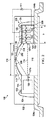
図1は、LED光源108及び横方向光センサ106を含む集積回路パッケージを形成するための1つ又は複数の導電体構造104を備えるモールディングされた構造102を含む光絶縁集積回路(IC)100を示す。光信号が、光源108の横方向信号出力面107aから集積回路パッケージ構造102のキャビティ110を介して、光路114に沿って、光センサ106の横方向センサ面107bに進行する。一例において、光源108は、第1のGaAs半導体ダイ又はその他の回路構造105において製造されるLEDであるが、他の実施形態において、レーザ、シリコンベースの光子エミッタ、又はその他の光源が用いられ得る。センサ106は、拡張された有効接合距離Dにわたって複数の横方向に離間されたpn接合を形成するように、pドープ領域101及び1つ又は複数のnドープ領域103によって形成される半導体構造を含む。図示される例において、光センサ106は、光信号を受信するために、光路114に面する横方向センサ面107bを形成する垂直の表側を備える第2のデバイス又は回路構造として製造される。光センサ106は、拡張された有効接合距離Dに沿って、1つ又は複数のpn接合を提供し、図1において、ダイオード111として概略が示される。回路構造105及び106は、個別に、ボンドワイヤ124によってリードフレーム構造の対応する導電体104a、104bに接続されるボンドパッド122を含む。一例における導体104a及び104bは、ホスト印刷回路基板(PCB、図示されない)にはんだ付けされ得るICピン又はパッドである。一例において、外部回路(図示されない)が、ペアの入力導体104aを介して、電気信号を光源108に提供し、光源108は、受信した電気信号に応答して、光信号を光路114に沿って生成する。また、この例において、IC100はボンドパッド122を含み、ボンドパッド122は、光センサ106から電気的出力信号を提供するために、対応するボンドワイヤ124によって、図1に概略で示されるリードフレーム導電体104bの第2のペアに電気的に接続される。図示される例における導体104bは、導体104aにおいて光源信号から絶縁されるセンサ106から電気信号を搬送するために、ホストPCBにはんだ付けされ得るIC100のパッド又はピンを提供する。この例の絶縁器IC100の絶縁電圧定格又は降伏電圧は、ガルバニック絶縁境界を横断して回路構造105及び106を分離する離間距離又は間隙距離116によって設定される。
FIG. 1 illustrates an opto-isolated integrated circuit (IC) 100 that includes a molded
信号出力面107a及びセンサ面107bは概して平行な平面にあり、キャビティ110において距離116、互いから離間される。他の可能な例において、これらの面107は平行である必要はない。光信号を受信するように、センサ面107bが少なくとも部分的に光源108に面しているような任意の相対的構成が用いられ得る。センサ面107bは、光信号の強度に対応する出力電気信号を生成するために、光を構造106に入射させる。センサ回路106は更に、センサ信号上で動作するように、インタフェース回路要素(図示されない)を含み得る。図1に示されるように、面107a及び107bのかなりの部分がキャビティ110内で露出されているが、これは全ての可能な実施形態の厳密な要求事項ではない。図1の例において、光源108及び光センサ106は、それらの間で電気的絶縁を提供するために、モールディングされたパッケージ構造102の内部キャビティ110において互いから離間されている。この例におけるキャビティ110は、ソリッドフリー(例えば、固体自由)な光路114を提供する。他の例(例えば、これ以降の図3及び図4)において、ガラス又はその他の光透過性固体構造が、光源108と光センサ106との間に提供され得る。一例におけるキャビティ110は、密封され、大気、又は有利にもガラス又は他の透明固体材料より低い誘電率を有し得るその他の光透過性の気体を含み、それによって光源108とセンサ106との間の容量結合を低減する。図1の例において、キャビティ110は、凹状の上面112を含むが、これは全ての可能な実装における厳密な要求事項ではない。一例において、キャビティ110は、堆積される犠牲的昇華材料を用いて、モールディングされた構造102の形成の間に形成され得、その後、ポート118を介する蒸発又は昇華によってソリッドフリーキャビティ110がつくられる。ポート118はその後、キャビティ110の密封を形成するように、テープ又は他の閉鎖構造120によって閉鎖され得る。或る例における絶縁間隙又は離間116は、ダイ又は回路構造105、106の1つの上の機械的特徴によって制御され、例えば、ダイ105とダイ106との間に延在する酸化物バンプ(図示されない)等によって間隙距離116が設定される。間隙116は、幾つかの例において、特定のサイズの充填材料をキャビティ110の形成に用いられる犠牲材料と混合することによって制御される。図示される例において、パッケージ構造102の内部表面は凹状部分を含み、凹状部分は、印刷プロセスを用いる等、製造中に犠牲材料を又は1つ又は複数の液滴として形成することによって提供される。そのため、この堆積された犠牲材料は部分的に凸状構造を形成し、この材料は、モールディングされたパッケージ構造材料102の形成の後、凹状の内側表面をそのままにして、昇華又は蒸発する。図1において斜線113で示されるように、キャビティ内側表面の凹状形状は、ダイ105及び106の縁部を超えて延在し得、光がLED光源105の上部から出ることやセンサダイ106の上部に入ることを可能にする。
The
一例におけるIC100は、光源108に接続される電気回路から、センサ106に接続される電気回路(図示されない)にデータ又は電力を伝達するための光絶縁回路である。光源108は、光路114に沿って、所与の波長λの光信号を生成する。一例において、光源は、約950nmの波長λで信号を提供する横方向LEDである。その他の任意の適切な光源波長λが用いられ得る。本明細書で用いられるように、所与の波長λの光信号は、指定された波長を意味し、また、指定された値の数パーセント以内又はLED又は光絶縁デバイスのために用いられる他の光源に関連する任意の適切な波長許容範囲等の、指定された値に近い他の波長を意味する。一例において、光源108は、光センサ106の半導体構造101、103における吸収深さを最大化するために、シリコンのバンドギャップエネルギーの直ぐ上のエネルギーを有する長い波長信号を提供する。シリコンのバンドギャップエネルギーより小さいエネルギーレベルを有する波長λは、シリコンとの相互作用が弱く、一方、シリコンのバンドギャップエネルギーよりも大きいか又ははるかに大きいエネルギーレベルを有するλは強力に吸収されるが、バンドギャップより大きいエネルギー部分は、電子が急速にサーマライズダウンするにつれて浪費される。或る例において、横方向デバイスは、最大捕捉を得るためにシリコン長さが増大され得るバンドギャップエネルギーにおける波長に対して最適である。
The
光センサ106は、所与の波長λの横方向に受け取られた光子の受け取り及び捕捉における動作に対して設計される。図1の例における光センサ106は、頂部T及び底部B、並びに、光源108から光信号を受信するためのセンサ面107bを提供するための少なくとも部分的に光路114に面する表側を有する半導体構造を含む。半導体構造は更に、表側から離間される裏側、及び、頂部Tと底部Bとの間に垂直に、表側と裏側との間に水平に延在する側面を含む。図示された例において、半導体構造は、概して平行な表側及び裏側を有する概して矩形であり、頂部及び底部は、概して平面状で互いに対して平行である。また、図示された例は、概して平面状の側面を提供する。しかしながら、他の半導体構造形状も用いられ得る。任意の適切な半導体構造が用いられ得る。或る例において、半導体構造はシリコン(Si)である。他の例において、ガリウム砒素(GaAs)又は他の適切な半導体材料が用いられ得る。
The
半導体構造は、ホウ素又は他のp型ドーパントを有するpドープ部分101を含む。pドープ部分101は、或る実装において、図1に示されるように、底部Bの少なくとも一部に沿って延在する。一例において、半導体構造の製造は、部分101を形成するためのpドープシリコン基板で開始する。p型部分は、底部Bから出てパッケージ電気コネクタ104bに電気的に接続される。他の例において、pドープ部分101を形成するために、p型ドーパントが注入及び/又は拡散によって半導体基板の中に導入される。また、半導体構造は、pドープ部分101に少なくとも部分的に隣接するリン又は他のn型ドーパントを含む、1つ又は複数のnドープ部分103を含む。nドープ部分は、頂部Tから出て、別のパッケージ電気コネクタ(図示されない)に対する電気的接続122及び124に電気的に接続する。nドープ部分又は部分103は、半導体構造内に少なくとも1つのpn接合を形成する。結果の1つ又は複数のpn接合は、半導体構造の表側と裏側との間で、有効接合距離D、延在する。或る例における有効接合距離Dは、所与の波長λに対応する半導体構造の吸収深さの定数K倍より大きく、Kは1より大きい。
The semiconductor structure includes a p-doped
本明細書において用いられるように、半導体構造101、103に対する吸収深さは、距離値(例えば、図1において、センサ面107bから右に延在して、半導体構造に入る)であり、それに対して、入射放射線強度が1/e又は約36%低減される。この距離において、電子/正孔対の生成を介してシリコン101、103によって吸収される光子エネルギーの量は、横方向センサ面107bにおいて受け取った所与の波長λの約64%とし得る。一例において、Kは5以上である。他の例において、Kは10以上である。更なる実装において、Kは20以上である。接合距離Dは、例えば、Kが1000未満であるような、所与のエンドユース用途の実用的な物理的限界の範囲内の任意の適切なサイズとし得る。一例におけるnドープ部分は、頂部Tの少なくとも一部分に沿って延在するが、これはすべての可能な実装の要求事項ではない。拡張された有効pn接合距離は、横方向センサ面107bにおいて受け取られた入射光子の高率の吸収を促進する。例えば、図9及び図10に関連してこれ以降に図示及び説明されるように、光子捕捉及び結果のキャリア生成は、半導体構造のセンサ面107bの入り口又はその近くで高い確率であり、また、光子捕捉の確率は、半導体構造の表側からの距離が増大するにつれて低下する。開示される横方向デバイスにおいて、横方向寸法は、標準の厚みのシリコンウエハの平面の(水平)距離である。多くの製造プロセスにおいて、シリコンウエハは約10ミリの厚みにバックグラインドされ、標準の垂直光起電センサは、約254ミクロンの経路長を有し得るだけである。また、この経路長の内、頂部20ミクロン程度のみが光子捕捉に対して有用である。極めて厚い、垂直シリコンのマルチ接合ピースをつくること、及びそのアセンブルされたダイスタックをその側面に置くことによって、長い接合がつくられ得る。しかしながら、これは、横方向デバイス構築に比べると、極めて非標準的であり、非実用的な方法である。
As used herein, the absorption depth for
半導体構造に、有効なpn接合距離Dの実質的に全てにわたって延在する又は分散される1つ又は複数のnドープ部分103を含ませることは、特定の半導体材料に対応する吸収深さ及び対応する所与の波長λに対してDを大きくすることによって高効率の光子捕捉確率を促進する。例えば、約950nmの波長λにおいて光子を送信するために、高効率LED光源108が用いられ得る。適切にドープされたp及びn部分101及び103を有するシリコン半導体構造を用いて、受け取った光子エネルギーの約64%が、950nm光源に対する最初の80μmの進行において吸収される。発明者は、5以上のKの場合に高吸収率が達成され、10以上のKを用いることによって更なる改善が達成されることを理解している。また、20以上のKの場合、ほぼ完全な(例えば、100%近い)吸収が達成される。図1の例において、有効なpn接合距離Dは、pドープ部分101の頂部に注入及び/又は拡散された、対応するnドープ領域103を介して、複数のpn接合を生成することによって実装される。図1の例は、距離Dの実質的に全てにわたってpn接合をつくるための5つのそのようなnドープ領域103を示すが、対応する多数のpn接合をつくるために、多数のnドープ領域103が用いられ得る。図示されたnドープ領域103は、横方向半導体構造の表側と裏側との間で実質的に均一に離間されているが、均一の離間は全ての可能な実装の厳密な要求事項ではなく、種々の実施形態において、複数の離間及び特徴サイズが用いられ得る。
Including a semiconductor structure with one or more n-doped
結果の構造101、103は、高い収集確率を促進するように、ほぼ直線のコリドーに沿って複数のpn接合を提供する。種々の実施形態において、複数のそのような半導体構造が用いられ得(例えば、図4)、対応する光コリドーが電気的に絶縁され得る。結果のpn拡張接合セルを任意の所望の直列及び/又は並列構成において接続するために、相互接続回路がIC100に提供され得る。また、個々の半導体構造は、受け取った光子エネルギーの大半の捕捉を促進するため、及び隣接する光回路から各チャネルを光絶縁するために内部反射を提供するように、上部及び下部(例えば、頂部及び底部)の反射材料又は構造109を含み得る。また、マルチチャネルの概念は、異なるチャネルの光絶縁が通信応用例に対するクロストークの最小化を促進する、電力伝達並びにデータ伝達応用例において用いるために拡張され得る。また、図1に示されるように、裏側において遭遇する全ての光子がセンサ面107bに向かって反射され、それによって更に収集効率が改善されるように、光反射材料109が半導体構造101、103の裏側に提供され得る。同様に、或る実施形態において、センサ構造によって収集される所与の入射光子の確率を更に高めるために、光反射材料が半導体構造101、103の側面(図示されない)に提供され得る。
The resulting
上述したように、或る例において、複数の半導体構造101、103が含まれ得、これらのセルは、所望の出力電圧及び/又は電力を達成するために、スタックされ得るか、又は、任意の適切な直列及び/又は並列様式で相互接続され得る。或る例(例えば、図6〜図8、及び図23)において、単一のnドープ部分103を用いることによって、接合距離Dを持つ単一のpn接合をつくるために、単一の拡張されたpn接合が個々の半導体構造101、103において提供される。他の例(例えば、図1〜図5、及び図12〜図22)において、各半導体構造101、103は、表側と裏側との間の有効接合距離Dの実質的に全てにわたって複数のpn接合をつくるために、n型ドーパントを含む複数のnドープ部分103を含む。結果の光センサ106は、或る応用例において、データ及び/又は電力伝達のために用いられ得る。また、拡張された接合横方向センサ構造106はまた、例えば、図22及び図23に関連して下記に更に説明する光子検出器システム等において、光子増倍器応用例に用いられ得る。従来のオプトカプラとは異なり、本開示の拡張された接合デバイス及びシステムは、電力供給応用例において高い電流伝達比(CTR)を促進し、従って、ガルバニック絶縁障壁によって分離される回路の高効率バイアスを促進する。また、図1の距離114は、所与の応用例に対する任意の所望の降伏電圧又は絶縁電圧定格に従ったサイズとし得る。また、この絶縁レベルの調整性は、従来の垂直配向オプトカプラの場合にそうであったようなIC100の垂直高さにおける増大を引き起こさない。
As mentioned above, in certain examples, a plurality of
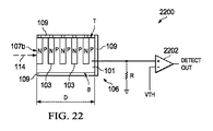
光センサ106の動作において、センサ面107bを介して横方向に受け取った入射光子は、ドープ領域101及び103によって形成される拡張されたpn接合又はその近くで吸収される。動作の一形態において、センサ106及びその対応する拡張されたpn接合は、光起電力モードで光ダイオードとして動作し、キャリア及び対応する電流フローを生成し、電力供給バイアス及び/又はデータ伝達において用いるための電気的出力信号を生成する。特に、一旦、充分なエネルギーの光子が受け取られると、半導体構造101、103における内部の光電気効果を介して、電子−正孔対がつくられる。拡張されたpn接合の空乏領域又はその近くで吸収が起こると、キャリアが、空乏領域の電界に従って接合から離れて移動し、その際、正孔はアノード(pドープ領域101)に向かって移動し、電子はカソード(一つ又は複数のnドープ領域103)に向かって移動する。このキャリア移動は電流フローを生成し、電流フローは、センサ106に接続される関連する回路に対する電気信号を生成するために用いられ得る。例えば、低ドロップアウト(LDO)レギュレータ又は他の電力供給回路が、センサ106に接続された外部回路に電力を供給するために、光生成された電流を用い得る。他の例において、センサ106によって生成された電流フローは、センサに接続された外部回路によって、受信したデータ信号として用いられ得る。図22及び図23に関連してこれ以降に説明されるように、例えば、シリコン光子増倍回路において、センサ回路106からの生成された信号が個々の受け取られた光子の検出を示すために用いられ得る。
In operation of the
図2は、上述したようなLED光源108及び拡張された接合横方向光センサ106を備える、別の例示の絶縁IC実施形態100を示す。この例において、キャビティ110の内部表面は、例えば、光路202に沿って、光源108から光センサ106に向かって光を反射する反射コーティング200を含む。一例における反射コーティング材料200は、モールディングされたパッケージ構造材料102をつくるモールディングプロセスの前に、凸状の犠牲昇華材料の上に堆積される。モールディングプロセス後の犠牲材料層の昇華により、残留反射材料層200の凹状表面によって少なくとも部分的に画定されるキャビティ110が残される。光源108によって生成された光信号の全て又は一部の光センサ106に向かう反射を促進する任意の適切な非導電材料200が用いられ得る。図2に示されるように、光源108からの光信号は、光路114に沿って、キャビティ110を介して、センサダイ106のセンサ面107bに対して直接進行し得、及び/又は、信号はまた、凹状表面112上の反射コーティング200を介して、反射された経路202に沿って進行し得る。他の可能な例において、キャビティ112の凹状表面112及び任意の対応する反射コーティング200は、光センサ半導体構造の頂部の少なくとも一部を露出させるように横方向に拡張され得、それにより、反射された光子が、センサ106における潜在的な捕捉のために、半導体構造の頂部に入ることを可能にする。
FIG. 2 illustrates another exemplary
図3は、上述したような光源108及び光センサ106を備える別の非限定的な例示の絶縁IC100を示す。この例において、光源108及び光センサ106の面107aと面107bとの間に、光透過性構造300が、光路114に沿って配置される。ガラス、ポリマー等の任意の適切な材料300が用いられ得る。
FIG. 3 illustrates another non-limiting exemplary
また、図4及び図5を参照すると、図4は、別の光絶縁IC実施形態100を示す。この例において、光センサ106は、複数の直列接続されたダイオードを含み、複数の直列接続されたダイオードの各々は、上述したように、対応する半導体構造401、402のp及びnドープ部分を含む。この例における光センサ111は、2つの(例えば、下部及び上部)基板又はダイ401及び402によって形成される2つの直列接続光ダイオードを含むが、2又はそれ以上の任意の数のそのようなスタックされたダイが用いられ得る。一例において、ダイ401、402は各々、例えば、対応する半導体構造の頂部T上の酸化物層502及び上部パッシベーション層504によって形成される、上部反射コーティング材料を含む。個々の半導体構造内に光子を含むために底部反射表面を形成するため、及び上部半導体構造/ダイ402を下部ダイ401に接着させるために、半導体構造の各々の底部B上に反射銀担持エポキシが用いられる。この例において、光センサ構造106はまた、任意の所望の増幅器、フィルタ、又は他のインタフェース回路(図示されない)を含む半導体基板を備えるベースダイ400を含み、下部センサダイ401は、取り付けのため及びダイ401における光子反射のために、光反射銀担持エポキシを用いて、ベースダイ400の頂部に取り付けられる。ダイ401及び402は、一例において、ベースダイ400より小さい垂直高さを持つようにバックグラインドされる。一例において、スタックされたダイ401及び402は各々、nドープ部分103に対して上方電気接続を提供するためのメタライゼーション構造を含み、ダイ401及び402を共に接合するために用いられる銀担持エポキシは、対応するダイオードを互いに直列に効率的に接続するため、下部ダイ401のnドープ部分から上部ダイ402のpドープ部分への電気的接続を提供し得る。一例において、個々のダイ401及び402は各々、約0.5Vの電圧信号を生成し、スタックされたダイ401及び402は、外部回路(例えば、1.0V)に対してより高い出力信号を提供するように直列に相互接続され得る。2つより多くのスタックされたダイを有する実施形態が、光源108からの光信号に応答して所望の出力信号レベルを達成するように、任意の所望の直列及び/又は並列構成において相互接続され得る。
Referring also to FIGS. 4 and 5, FIG. 4 illustrates another opto-isolated
図6及び図7は、光センサ106において複数のスタックされたダイオードを用いる別の絶縁IC例100を示す。図6における第2の回路構造106は、単一のpドープ部分及び単一の拡張されたnドープ部分を個々に含む垂直ダイオードを備える複数ダイ構造である。上述の実施形態と同様に、この例は、所与の波長λに対応する半導体構造に対する吸収深さより長い有効接合距離Dを有する拡張された横方向pn接合構造を提供する。図6及び図7におけるセンサ構造は、ベースダイ600上に形成される4個のスタックされたダイ601、602、603、及び604を含むが、任意の数のダイが用いられ得る。図7は、種々のダイ601〜604における、幾つかの例示の光進行経路を示す。
6 and 7 show another example of an
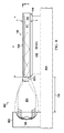
ここで図8〜図10を参照すると、図8は、放物面リフレクタミラー構造802を備えるLED光源108を含む例示の光絶縁回路800を示す。一例において、光源108は、定格100mAにおいて50mWのOSRAM SFH−4441 940nm LEDである。光カプラ構造804が、LED/ミラー構成要素108、802と、上述したような単一のpドープ部分101及び単一の拡張された長いのnドープ部分103を含む半導体構造のセンサ面107bとの間に提供される。この例において、Kは約7である。この例は、捕捉確率の増大のため、図8において簡略化された形式で示されるように、光子反射を促進するために、半導体構造の頂部T上の酸化物等の反射コーティング材料109、並びに、底部B上の反射材料109(例えば、反射エポキシ)を含む。半導体構造101、103は、エポキシ109を介してペデスタル808に取り付けられ、光源及びセンサ構造は、絶縁回路800の絶縁レベルを設定するための離間又は間隙距離116を画定するように、離間された関係でベース806に取り付けられる。或る例において、頂部側Tにおけるn及びp領域に対して電気接続(図示されない)がなされる。
Referring now to FIGS. 8-10, FIG. 8 illustrates an exemplary opto-isolated
図9は、図8における線9−9に沿った半導体構造101、103の平面図を示す。この構造は、センサ面107bに入射する光子の捕捉に基づいて光生成された電流を収集するために、nドープ部分103の対応するエリアに接続される1つ又は複数の導電タップ904を含む。
FIG. 9 shows a plan view of the
図10は、図9におけるタップ位置904でのタップ電流を、センサ面107bからの距離の関数として、μaで表す曲線1002を示すグラフ1000を提供する。上述したように、光子捕捉の確率及び従って光子生成されたタップ電流の大きさは、センサ面107b又はその近くで最も高く、半導体構造における距離が増大するにつれて下がる。この例において、生成された総タップ電流の約64%が、所与の半導体材料及び所与の波長λに対する吸収距離に対応する、センサ面107bからの初期距離902にわたって生成される。
FIG. 10 provides a
図11は、例示の吸収深さ曲線1102をシリコン半導体構造101、103に対する波長λ(μm)の関数として含むグラフ1100を示す。この例において、940nmの光子波長において入射する光子の64%吸収に対する深さは、約95μmである。この原理を用い、所与の光源波長λ及び半導体材料に対する所望の収集効率目標を達成するために充分な有効接合距離Dを用いて、所与の光センサ106が設計され得る。
FIG. 11 shows a
また、図12〜図21を参照すると、拡張された接合光センサ106を用いて、種々の異なる回路構造及びデバイスがつくられ得る。上述したように、或る例は、潜在的に多数の個別のセンサセルを含み、センサセルの各々が、横方向センサ面107bと、所与の光源波長λに対する対応する半導体材料の吸収深さより長い拡張された有効接合距離Dとを有するセルをつくるために、pドープ部分及び1つ又は複数のnドープ部分を備える半導体構造を含む。直列及び/又は並列構成において相互接続された複数の横方向セルの組み合わせは、本明細書において、多段光起電力(LMSPV)センサ構造106と称される。
Referring also to FIGS. 12-21, a variety of different circuit structures and devices can be created using the expanded junction
図12は、集積回路ダイ又はパッケージされたマルチダイデバイス1201上に実装されるセンサ構造を含む例示の絶縁された低ドロップアウト(LDO)レギュレータデバイス1200を図示する。この例において、センサ回路106は、上述したように、横方向センサ面107bから光を受け取るためのLMSPV構造として形成される。LMSPV106のn及びpドープ部分は、LMSPV106の複数の半導体構造101、103のpn接合を電気的に相互接続するためのスイッチング回路1202に電気的に接続される。一例において、スイッチング回路1202は、デバイス1201が、構成可能な電圧及び電流値を有する出力信号(例えば、図12における出力電圧VO)を提供できるよう、直列及び/又は並列相互接続に対する変更を可能にするように、プログラム可能又はその他の方式で構成可能である。スイッチング回路1202を介してLMSPV106から提供される電気信号が、LDOレギュレータ回路1204に送られる。レギュレータ回路1204は、負荷(図示されない)を駆動するために出力信号VOを提供する。デバイス1200は、有利にも、ガルバニック絶縁障壁を横断して光絶縁を有する一層高効率の電力供給を実装するために、整合された光源(図示されない)とLMSPV光センサ106との間で高い電流伝達比を提供する。
FIG. 12 illustrates an exemplary isolated low dropout (LDO)
図13は、負荷に対して電力を選択的にオンにするために、パルスオン又はオフされる光信号を受け取るためのセンサ面107bを備えるLMSPV106を含む絶縁されたソリッドステートリレー(SSR)デバイス1300を示す。一例において、デバイス1300は、LMSPV106、上述したような直列/並列スイッチング回路1202、ホストスワップ機能性を実装するための特定用途向けアナログ回路1302、及び電力スイッチ1304を含んで、単一の集積回路ダイ又はパッケージされた複数ダイ構造1301内にパッケージされる。一例において、デバイス1300は、絶縁電力スイッチのために用いられ得る。デバイス1300は、有利にも、電力供給回路の二次側から電気的に絶縁される信号源からLMSPV106を介してオン又はオフ制御シグナリングの提供を促進する。
FIG. 13 illustrates an isolated solid state relay (SSR)
図14は、単一の集積回路ダイ、又は複数のLMSPV回路106、及び対応する横方向センサ面107b、並びに上部及び下部ホールドアップキャパシタ1402、及びゲートドライブ回路1404、及び負荷を制御するためのDC又はAC電力スイッチ1304を備えるパッケージされた複数ダイ構造1401内にパッケージされる絶縁されたラッチングSSRデバイス1400を示す。デバイス1401は、上述したように、センサ面107bにおいてLED光源105、108から光を受け取る。ホールドアップキャパシタ1402は、LMSPV構造から得た出力信号のラッチングを提供して、受信した光信号を起動させ及び電力スイッチ1304をラッチさせる。
FIG. 14 shows a single integrated circuit die or
図15〜図17は、光リボン又はファイバ1508との組み合わせにおいて、図12の例示のLDOレギュレータデバイス1200を用いる光的に絶縁された電力供給ソリューションを図示する。図15及び図16はそれぞれ、モールディングされた化合物材料1502内にパッケージされる絶縁された電力供給デバイス1500の側面図及び平面図を示す。光源側回路1501が、ホスト印刷回路基板(図示されない)にはんだ付けされ得るピン又はパッド等のリード1504及び1506、光源(例えば、サイド又は横方向発光LED)105、108、及び光リボン又はファイバ1508の入力側に接続される光結合材料804を有するリードフレーム構造を含む。光リボン又はファイバ1508の出力端部は、対応する光結合材料804を介して、LMSPV構造106の横方向センサ面107bに接続される。電力供給デバイス1500はまた、図12に関連して上述したようなLDOレギュレータデバイス1200を含む、負荷又は出力側回路1511を含む。この例におけるレギュレータデバイス1200は、ホスト印刷回路基板に接続される被駆動負荷回路に電気出力信号(例えば、出力電圧又は電流)を提供するためのリード1510及び1512を含む出力側リードフレーム構造に取り付けられる。図15及び図16におけるデバイス1500は、有利にも、単一デバイスにおいて光電力供給絶縁ソリューションを提供し、また、有利にも、LMSPV構造106の高電力伝達比及び高効率利点を用いて、電力伝達のための変圧器絶縁技法の欠点であったスペース、コスト、電磁干渉の問題なしに、ガルバニック絶縁障壁を横断して電力を伝達する。
15-17 illustrate an optically isolated power supply solution using the exemplary
図17は、2つの離れたシステム間の電力伝達のための別の光絶縁システム1700である。この例において、光源側回路要素1501は、第1の集積回路ダイ、又はリード1504及び1506を備えるリードフレーム構造を含むパッケージされた複数ダイ構造1701内にパッケージされる。光ファイバ又はリボン1508が、第1の構造1701を、第2のICダイに、又はリード1510及び1512、及び上述のレギュレータデバイス1200を備える第2のリードフレーム構造を含むパッケージされた複数ダイ構造1702に接続する。光絶縁システム1700は、ダイ構造1701とダイ構造1702との間の光リボン又はファイバ1508のシンプルな接続によって、絶縁障壁を横断して負荷をバイアス又は駆動するための集積ソリューションを提供する。
FIG. 17 is another
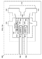
図18は、LDOレギュレータシステム1800を実装する負荷側回路1511の別の例を示す。この例における負荷側回路1511は、LMSPV構造106、並びに、スイッチング回路1202及び上述したようなレギュレータ回路1204を備えるレギュレータ構造1200を含む。この例における回路及び構造106、1202、及び1204は、単一の半導体ダイ1200上につくられる。この例は更に、光絶縁障壁構造1802を含む。一例において、光絶縁障壁構造1802は、半導体ダイのトレンチに形成されるブラックポリマー又は他の遮光材料を含む。一例において、p及びnドープ部分101及び103を含むLMSPV半導体構造106は、スイッチング回路要素1202及びレギュレータ回路要素1204とともに、シリコン構造内に形成される。LMSPV構造106をスイッチング回路120から分離するようにするようにトレンチが形成され、トレンチはブラックポリマーで充填される。その後、ダイは、トレンチにおけるポリマーを露出するようにバックグラインドされる。結果の構造は、ポリマーによって共に保持され、ポリマーは、LMSPV構造106をスイッチング回路1202及びLDO回路1204から絶縁するための光障壁を形成する。
FIG. 18 shows another example of the
ここで図19及び図20を参照すると、光絶縁技法及び図18の障壁構造1802は、異なるチャネル又は異なる回路を光的に絶縁することが望ましい他の実施形態において用いられ得る。図19は、複数の光チャネルを含む別のレギュレータシステム1900を示す。この例における各チャネルは、対応する光ファイバ又はリボン1508を介して光信号を受信するLMSPVスタック構造106を含む。この例において、LMSPVセンサ構造106の各々の上部及び下部縁部に沿って、ブラックポリマー充填トレンチ絶縁構造1802が形成される。これは、LMSPVセクション又はセル106間の光クロストークを効果的に防止し、また、デバイス1200において形成されるスイッチング回路1202及び/又はLDOレギュレータ回路要素1204との光干渉を防止する。
Referring now to FIGS. 19 and 20, the optical isolation technique and the
図20は、2つの図示されたLMSPV部分106内に光信号を制限するために、上述のブラックポリマー充填光絶縁構造1802を含む別の例を示す。この例において、反射材料充填構造2002が、光チャネルの各々のLMSPV部分106の周りに形成される。上述したように、反射材料の使用は、半導体材料及び拡張されたpn接合内の光子捕捉に対する更なる機会を促進することによってLMSPV構造106の捕捉効率を高める。一実装において、反射器構造2002は、LMSPV構造106の長さの大半にわたる直線部分を含み、LMSPV構造の裏側は、放物面形状の部分等の円弧部分を含む。一例において、構造2002は、光絶縁構造1802を形成する際に用いられるものと類似の選択的ディープエッチングプロセスによって形成される。LMSPV構成要素106の製造後、半導体構造にディープトレンチが形成され、トレンチはガラス等の光反射材料で充填される。ダイは、その後、ガラスを露出するようにバックグラインドされ、半導体構造及びその拡張されたpn接合の3つの側面を横方向に囲む反射構造2002を備える強化されたLMSPV構造106が残される。また、隣接する光チャネル間においてブラックポリマー充填構造1802は、光チャネル間の光クロストークを軽減又は回避するための光絶縁を提供する。また、上述したように、個々のLMSPV構造106の頂部及び底部に、例えば、底部Bの上の反射エポキシ、及び頂部側T(例えば、図1における109)上に形成される酸化物層又は材料等の反射材料が追加され得る。
FIG. 20 shows another example that includes the black polymer-filled
ここで図21〜図23を参照すると、シリコン光増倍器デバイス(SiPMD)の特異な構成が示される。本開示は、光子がシリコンアレイの頂部表面に入る従来の方式では用いられないSiPMDを提供する。その代わりに、上述された例示のデバイスのように、SiPMDsデバイスは、側部又は縁部において、拡張された収集距離に光子を入らせる。SiPMDは、単一の入力光子を、電子−正孔対が生成されるアレイのPNセルにおいて電子のアバランシェに増倍する。図21の例において、各アレイセルは次のセルから隔離され、従って、アバランシェは構造全体を横断して伝播することはない。セルがそのアバランシェ降伏の近くで動作されるので、アバランシェが起こり、そのため、アバランシェ電流フローを起こすには1つの光子で充分である。これは、各セルにおいて高利得増幅を生成し、これを高感度検出器にする。一旦アバランシェにトリップすると、セルはリセットされる必要があり、そのため、図22及び図23に示されるように、各セルに対して直列クエンチング抵抗器Rがある。クエンチング回路抵抗器Rは、セル電圧を充分に低下させ、それによってアバランシェから脱出させる。これらのセル及びクエンチング抵抗器は全て並列であり、そのため、組み合わされた出力電流は、光子密度に非常に大きなゲインファクタを掛けたものを表し、回路は、動作するためにバイアスを用いる。また、横方向の構造は、検出器の感度を高める。 Referring now to FIGS. 21-23, a unique configuration of a silicon photomultiplier device (SiPMD) is shown. The present disclosure provides a SiPMD that is not used in a conventional manner where photons enter the top surface of the silicon array. Instead, like the exemplary devices described above, SiPMDs devices allow photons to enter the extended collection distance at the sides or edges. SiPMD multiplies a single input photon to an avalanche of electrons in the PN cells of the array where electron-hole pairs are created. In the example of FIG. 21, each array cell is isolated from the next cell, so the avalanche does not propagate across the entire structure. Avalanche occurs because the cell is operated near its avalanche breakdown, so one photon is sufficient to cause avalanche current flow. This creates a high gain amplification in each cell, making it a sensitive detector. Once tripped to the avalanche, the cells need to be reset, so there is a series quenching resistor R for each cell, as shown in FIGS. The quenching circuit resistor R causes the cell voltage to drop sufficiently, thereby exiting the avalanche. These cells and the quenching resistor are all in parallel, so the combined output current represents the photon density multiplied by a very large gain factor, and the circuit uses a bias to operate. Also, the lateral structure increases the sensitivity of the detector.
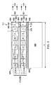
図21は、アレイに形成される複数の光センサ半導体構造を含む例示のLMSPVアレイ構造2100を図示する。LMSPV構造2100は、横方向センサ面107b、及び上述したように、拡張された有効接合距離Dを有する多数の個々のpnセルのマトリクス又はアレイを含む。この例において、アレイの個々のセルは単一のnドープ部分103を含み、単一のnドープ部分103は、実質的に、拡張された有効接合距離Dにわたって配置される個々のpn接合のアレイをつくるように、隔離されたpドープ領域101において形成される。図21は更に、一例におけるアレイセルの2つの列及び幾つかの行の一部のブレークアウト図を図示する。また、図22及び図23に関連してこれ以降に説明するように、LMSPV構造2100は光子センサ応用例にも用いられ得る。
FIG. 21 illustrates an exemplary LMSPV array structure 2100 that includes a plurality of photosensor semiconductor structures formed in an array. The LMSPV structure 2100 includes a
図22及び図23に概略的に示されるように、LMSPV構造106は、複数のセルを備えるアレイであるか、pドープ部分101及び拡張された接合を形成するための1つ又は複数のnドープ部分103を有する単一の半導体構造106であるかに関わらず、光子検知システム及び回路に用いられ得る。図22は、上述したような、pドープ部分101内に配置される複数のnドープ部分103を含む半導体構造101、103を備える例示の光子検出器回路2200を示す。この構造は、光路114に沿って光子を受け取るための横方向センサ面107bを持つ拡張された接合光センサ106を形成する。センサ構造106は、入ってくる光信号の所与の波長λに対応する半導体構造に対する吸収深さに定数Kを掛けた有効接合距離Dを有する。図23における回路2300は、単一のnドープ部分103を有する拡張された接合光センサ回路106を用いる類似の配置を示す。図22及び図23における検出器回路2200及び2300における光センサは、等価寄生キャパシタ、ダイオード、及びアレイの各ダイオードセルにおける抵抗器を含み、これらは、クエンチング回路を形成し、その際、キャパシタCが、pドープ部分101とnドープ部分103との間で、センサ回路ダイオード111に並列に結合され、並びに、抵抗器Rがバイアス電圧VBIASとnドープ部分103との間に結合される。結果の構造は、横方向センサ構造106において小数の光子を検出するため、又は単一の光子の受け取りでさえも検出するためのクエンチング回路を形成する。動作において、抵抗器Rに対するバイアス電圧の印加はキャパシタCを充電し、一方、センサ回路ダイオード111は逆バイアスされる。バイアス電圧VBIASは、キャパシタCを、ダイオード111のアバランシェ定格のすぐ下のレベルまで充電する(一方、ダイオード111は導通しない)ように、センサ回路ダイオード111の仕様に対応するレベルに設定される。寄生キャパシタCが充電されると、回路2200は、センサ面107bにおいて光路114に沿って1つ又は複数の光子を受け取る準備ができる。センサ構造106における入射光子の捕捉に成功すると、pn接合にアバランシェ電流を導通させ、寄生キャパシタCを放電させる。寄生キャパシタCが、ダイオード111のアバランシェ閾値の下のレベルまで放電すると、ダイオード111は導通を中止し、寄生抵抗器RはキャパシタCを再び充電させる。寄生キャパシタCの放電/充電は、検出器回路2200、2300による光子の捕捉を表す信号をつくる。この増大された電流フローに基づいて検出器出力信号を生成するために電流検知閾値比較が用いられ得る。受け取った電流スパイクに応答して電圧信号を設定するために、検知抵抗器RSが比較器2202の+入力から回路接地基準に接続される。図22及び図23において、pドープ部分101は、信号電圧を受け取るために、電圧比較器2202の非反転(+)入力に接続される。比較器2202は、信号電圧を閾値電圧VTHと比較して、電流スパイクに応答して、検出器出力信号DETECT OUTを生成する。キャパシタCの放電/充電によって生成される電流信号が、電子−正孔対の生成によってセンサ構造106において生成されるキャリア電流よりもずっと大きいので、回路要素2200、2300は、光子検出又は他の有用な応用例において用いられ得る光子増倍回路を提供する。検出器アレイは個々の光子を検出するので、光子源に対して低効率のエミッタを用いることも可能である。これは、GaAs LEDの代わりに、低強度IR放射に対して、順バイアスのシリコンpn接合エミッタを備える標準シリコンを用いることを可能にする。低強度可視光を発するために、逆バイアスされたアバランシェ又はツェナー接合も用いられ得る。
As schematically shown in FIGS. 22 and 23, the
開示される例は、拡張された長さの有効pn接合の中への横方向光子入射を備える、高効率横方向PVセルを提供する。或る例において、有効な横方向接合距離Dは、高い収集効率を促進するために、所与の波長λの光子の吸収深さの倍数に設定される。これは、光センサ106の半導体構造における電子−正孔対生成に対する機会を大きく増大する。開示される例は、光チャネルを横断する低電力信号伝達において利点を提供し、ガルバニック絶縁障壁を横断する電力の高効率光伝達を可能にする。また、開示される概念は、光子検出器又は光子増倍器において有用性を見出す。或る構成において、より高いレベルの電力供給のために、多くのセンサセル106が相互接続され、各セルが低コスト構成である。個々の光起電力セル106が、酸化物及び/又は反射エポキシを介して、頂部T、底部B、裏側、及び横方向の側面に光反射材料109を含み得る場合は、低コストのスタック構成が可能であり、その際、負の(n型)ノードが1つ又は複数の接着パッドによって頂部T上に接続され、半導体材料における正の(p型)が底部B上に接続される。この例示の構成は、導電エポキシを備えるシンプルなダイスタッキングが、結果の感光性ダイオードを任意の所望の様式で相互接続することを可能にする。開示される例は、従来の光絶縁技法及びデバイスに比べて、光子から電気への電力伝達に対して、潜在的に大きな効率改善を提供する。また、横方向光子伝達は、光源108と光センサ106との間の間隔を制御することによって異なる絶縁電圧定格に容易に適応し、任意の適切な光送信媒体(例えば、ガラス、空気、ポリマー)を提供するための能力を備え、また、光ファイバ又は光リボンを用いて、光源とセンサを大きな距離分離することによって、極めて大きい電圧分離定格が達成され得る。
The disclosed example provides a high efficiency lateral PV cell with lateral photon incidence into an extended length effective pn junction. In one example, the effective lateral junction distance D is set to a multiple of the absorption depth of a photon of a given wavelength λ to promote high collection efficiency. This greatly increases the opportunity for electron-hole pair generation in the semiconductor structure of the
上記の例は、本開示の種々の観点の幾つかの可能な実施形態の例示に過ぎず、当業者であれば、この明細書及び添付の図面を読み理解することによって、等価の改変及び/又は変更が思いつくであろう。特許請求の範囲内で、説明した実施形態における変更が可能であり、他の実施形態が可能である。 The above examples are merely illustrative of some of the possible embodiments of the various aspects of the present disclosure, and those of ordinary skill in the art will appreciate, reading and understanding this specification and the accompanying drawings, that equivalent modifications and / or Or a change will come up. Within the scope of the claims, modifications in the described embodiments are possible, and other embodiments are possible.
Claims (20)
所与の波長の光信号を光路に沿って生成するように構成される光源、及び
前記光源から光チャネル距離、離間される光センサを含み、前記光センサが
半導体構造を含み、前記半導体構造が、
頂部と、
底部と、
前記光信号を受信するためのセンサ面を提供するように、前記光路に少なくとも部分的に面する表側と、
前記表側から離間される裏側と、
前記頂部と前記底部との間で垂直に延在する複数の側面であって、前記側面が前記表側と前記裏側との間で水平に延在する、前記複数の側面と、
p型ドーパントを含むpドープ部分であって、前記底部の少なくとも一部に沿って延在する前記pドープ部分と、
前記表側と前記裏側との間で或る有効接合距離延在する少なくとも1つのpn接合を形成するように、前記pドープ部分に少なくとも部分的に隣接するn型ドーパントを含むnドープ部分であって、前記nドープ部分が、前記頂部の少なくとも一部分に沿って延在し、前記有効接合距離が前記所与の波長に対応する前記半導体構造に対する吸収深さの定数K倍より大きく、Kが5以上である、前記nドープ部分と、
を含む、
絶縁回路。 An insulation circuit,
A light source configured to generate an optical signal of a given wavelength along an optical path; and an optical sensor spaced an optical channel distance from the light source, wherein the optical sensor comprises a semiconductor structure, wherein the semiconductor structure comprises ,
The top,
The bottom,
A front side at least partially facing the optical path, so as to provide a sensor surface for receiving the optical signal;
A back side separated from the front side,
A plurality of side surfaces extending vertically between the top and the bottom, wherein the side surfaces extend horizontally between the front side and the back side,
a p-doped portion comprising a p-type dopant, wherein the p-doped portion extends along at least a portion of the bottom;
An n-doped portion including an n-type dopant at least partially adjacent to the p-doped portion to form at least one pn junction extending an effective junction distance between the front side and the back side. The n-doped portion extends along at least a portion of the top, the effective junction distance is greater than a constant K times the absorption depth for the semiconductor structure corresponding to the given wavelength, and K is greater than or equal to 5 The n-doped portion;
including,
Insulation circuit.
各半導体構造が、
頂部と、
底部と、
前記光信号を受信するためのセンサ面を提供するように、前記光路に少なくとも部分的に面する表側と、
前記表側から離間される裏側と、
前記頂部と前記底部との間で垂直に延在する複数の側面であって、前記側面が前記表側と前記裏側との間で水平に延在する、前記複数の側面と、
p型ドーパントを含むpドープ部分であって、前記底部の少なくとも一部に沿って延在する前記pドープ部分と、
前記表側と前記裏側との間で或る有効接合距離延在する少なくとも1つのpn接合を形成するように、前記pドープ部分に少なくとも部分的に隣接するn型ドーパントを含むnドープ部分であって、前記nドープ部分が、前記頂部の少なくとも一部分に沿って延在し、前記有効接合距離が前記所与の波長に対応する前記半導体構造に対する吸収深さの定数K倍より大きく、Kが5以上である、前記nドープ部分と、
を含む、
絶縁回路。 2. The insulation circuit according to claim 1, wherein the optical sensor includes a plurality of semiconductor structures,
Each semiconductor structure is
The top,
The bottom,
A front side at least partially facing the optical path, so as to provide a sensor surface for receiving the optical signal;
A back side separated from the front side,
A plurality of side surfaces extending vertically between the top and the bottom, wherein the side surfaces extend horizontally between the front side and the back side,
a p-doped portion comprising a p-type dopant, wherein the p-doped portion extends along at least a portion of the bottom;
An n-doped portion including an n-type dopant at least partially adjacent to the p-doped portion to form at least one pn junction extending an effective junction distance between the front side and the back side. The n-doped portion extends along at least a portion of the top, the effective junction distance is greater than a constant K times the absorption depth for the semiconductor structure corresponding to the given wavelength, and K is greater than or equal to 5 The n-doped portion;
including,
Insulation circuit.
複数の導電体を含むリードフレーム構造であって、前記光源が、前記リードフレーム構造の前記導電体の第1のペアに電気的に結合され、前記光センサが、前記リードフレーム構造の前記導電体の第2のペアに電気的に結合される、前記リードフレーム構造、及び
前記光源、前記光センサ、及び前記リードフレーム構造の一部を封入するモールディングされたパッケージ構造、
を更に含み、
前記モールディングされたパッケージ構造が、前記光源及び前記光センサに対して外部接続を可能にするために、前記導電体の前記第1及び第2のペアの部分を露出させる、
絶縁回路。 The insulation circuit according to claim 1, wherein
A leadframe structure including a plurality of electrical conductors, wherein the light source is electrically coupled to a first pair of the electrical conductors of the leadframe structure, and wherein the optical sensor is connected to the electrical conductor of the leadframe structure. A lead package structure electrically coupled to a second pair of the light source, the light sensor, and a molded package structure enclosing a portion of the lead frame structure;
Further comprising
The molded package structure exposing portions of the first and second pairs of conductors to allow external connections to the light source and the light sensor;
Insulation circuit.
前記pドープ部分と前記nドープ部分との間に結合されるキャパシタ、及び
バイアス電圧と前記nドープ部分との間に結合される抵抗器、
を更に含み、
前記抵抗器が、前記キャパシタを、前記pn接合をアバランシェ電圧の近くにバイアスさせる電圧まで充電させて前記pn接合による光子の捕捉を可能にさせ、前記pn接合にアバランシェ電流を導通させ、前記キャパシタを放電させ、前記光子の捕捉を表す信号を生成させる、
絶縁回路。 The insulation circuit according to claim 1, wherein the optical sensor comprises:
A capacitor coupled between the p-doped portion and the n-doped portion; and a resistor coupled between a bias voltage and the n-doped portion;
Further comprising
The resistor charges the capacitor to a voltage that biases the pn junction near an avalanche voltage to enable photon capture by the pn junction, conduct avalanche current through the pn junction, Discharging to generate a signal representative of the capture of the photons;
Insulation circuit.
半導体構造、及び前記半導体構造に形成されるpn接合を含み、
前記半導体構造が、
頂部と、
底部と、
前記光路に少なくとも部分的に面する表側と、
前記表側から離間される裏側と、
前記頂部と前記底部との間で垂直に延在する複数の側面であって、前記側面が前記表側と前記裏側との間で水平に延在する、前記複数の側面と、
を含み、
前記pn接合が、前記表側と前記裏側との間で、前記所与の波長に対応する前記半導体構造に対する吸収深さの定数K倍より大きい有効接合距離延在し、Kが5以上である、
光センサ回路。 An optical sensor circuit for detecting an optical signal of a given wavelength along an optical path,
A semiconductor structure, and a pn junction formed in the semiconductor structure;
The semiconductor structure is
The top,
The bottom,
A front side at least partially facing the optical path;
A back side separated from the front side,
A plurality of side surfaces extending vertically between the top and the bottom, wherein the side surfaces extend horizontally between the front side and the back side,
Including
The pn junction extends an effective junction distance between the front side and the back side that is greater than a constant K times an absorption depth for the semiconductor structure corresponding to the given wavelength, and K is 5 or more;
Optical sensor circuit.
p型ドーパントを含むpドープ部分であって、前記底部の少なくとも一部に沿って延在する前記pドープ部分、及び
前記pn接合を形成するために前記pドープ部分に少なくとも部分的に隣接する前記頂部の少なくとも一部分に沿って延在する、n型ドーパントを含むnドープ部分を含む、光センサ回路。 The optical sensor circuit according to claim 15, wherein the pn junction is:
a p-doped portion including a p-type dopant, the p-doped portion extending along at least a portion of the bottom, and the p-doped portion at least partially adjacent to the p-doped portion to form the pn junction. An optical sensor circuit including an n-doped portion including an n-type dopant extending along at least a portion of the top.
前記pn接合のpドープ部分と前記pn接合のnドープ部分との間に結合されるキャパシタ、及び
バイアス電圧と前記nドープ部分との間に結合される抵抗器、
を更に含み、
前記抵抗器が、前記キャパシタを、前記pn接合をアバランシェ電圧の近くにバイアスさせる電圧まで充電させて前記pn接合による光子の捕捉を可能にさせ、前記pn接合にアバランシェ電流を導通させ、前記キャパシタを放電させ、前記光子の捕捉を表す信号を生成させる、
光センサ回路。 The optical sensor circuit according to claim 15, wherein
A capacitor coupled between the p-doped portion of the pn junction and the n-doped portion of the pn junction; and a resistor coupled between a bias voltage and the n-doped portion;
Further comprising
The resistor charges the capacitor to a voltage that biases the pn junction near an avalanche voltage to enable photon capture by the pn junction, conduct avalanche current through the pn junction, Discharging to generate a signal representative of the capture of the photons;
Optical sensor circuit.
複数のシリコン構造、及び
回路、
を含み、
前記複数のシリコン構造が個別に、
頂部、
底部、
所与の波長の光子を受け取るためのセンサ面を提供するための表側と、
前記表側から離間される裏側、
前記頂部と前記底部との間で垂直に延在する複数の側面、及び
前記所与の波長に対応するシリコンに対する吸収深さの定数K倍より大きい有効接合距離、前記表側と前記裏側との間に延在する接合領域、
を含み、Kが5以上であり、前記接合領域が、前記表側と前記裏側との間の前記有効接合距離の実質的に全体にわたって複数のpn接合を提供するために、前記シリコン構造におけるpドープ部分と、前記pドープ部分に形成される複数のnドープ部分とを含み、
前記回路が、前記pn接合又は前記pn接合の近くでの前記光子の捕捉を示す電気信号を提供するために、前記複数の半導体構造の前記pn接合を電気的に相互接続させるためである、
光起電センサシステム。 A lateral multi-stage photovoltaic sensor system,
Multiple silicon structures and circuits,
Including
Wherein the plurality of silicon structures are individually
The top,
bottom,
A front side to provide a sensor surface for receiving photons of a given wavelength;
The back side separated from the front side,
A plurality of sides extending vertically between the top and the bottom; and an effective junction distance greater than a constant K times the absorption depth for silicon corresponding to the given wavelength, between the front side and the back side. A joining region extending to
Wherein K is 5 or more, and wherein the junction region provides a plurality of pn junctions in the silicon structure to provide a plurality of pn junctions over substantially the entire effective junction distance between the front side and the back side. A portion and a plurality of n-doped portions formed in the p-doped portion,
The circuit for electrically interconnecting the pn junctions of the plurality of semiconductor structures to provide an electrical signal indicative of the capture of the photon at or near the pn junction.
Photovoltaic sensor system.
Priority Applications (1)
| Application Number | Priority Date | Filing Date | Title |
|---|---|---|---|
| JP2023180857A JP2023182806A (en) | 2016-12-30 | 2023-10-20 | Optical isolation system, circuit, and photon detector with extended lateral p-n junction |
Applications Claiming Priority (5)
| Application Number | Priority Date | Filing Date | Title |
|---|---|---|---|
| US15/395,584 | 2016-12-30 | ||
| US15/395,584 US10074639B2 (en) | 2016-12-30 | 2016-12-30 | Isolator integrated circuits with package structure cavity and fabrication methods |
| US15/612,327 US10411150B2 (en) | 2016-12-30 | 2017-06-02 | Optical isolation systems and circuits and photon detectors with extended lateral P-N junctions |
| US15/612,327 | 2017-06-02 | ||
| PCT/US2017/068997 WO2018126161A1 (en) | 2016-12-30 | 2017-12-29 | Optical isolation systems and circuits and photon detectors with extended lateral p-n junctions |
Related Child Applications (1)
| Application Number | Title | Priority Date | Filing Date |
|---|---|---|---|
| JP2023180857A Division JP2023182806A (en) | 2016-12-30 | 2023-10-20 | Optical isolation system, circuit, and photon detector with extended lateral p-n junction |
Publications (2)
| Publication Number | Publication Date |
|---|---|
| JP2020507203A true JP2020507203A (en) | 2020-03-05 |
| JP2020507203A5 JP2020507203A5 (en) | 2021-02-12 |
Family
ID=62710085
Family Applications (2)
| Application Number | Title | Priority Date | Filing Date |
|---|---|---|---|
| JP2019536064A Pending JP2020507203A (en) | 2016-12-30 | 2017-12-29 | Optical isolation system and circuit, and photon detector with extended lateral pn junction |
| JP2023180857A Pending JP2023182806A (en) | 2016-12-30 | 2023-10-20 | Optical isolation system, circuit, and photon detector with extended lateral p-n junction |
Family Applications After (1)
| Application Number | Title | Priority Date | Filing Date |
|---|---|---|---|
| JP2023180857A Pending JP2023182806A (en) | 2016-12-30 | 2023-10-20 | Optical isolation system, circuit, and photon detector with extended lateral p-n junction |
Country Status (5)
| Country | Link |
|---|---|
| US (1) | US10411150B2 (en) |
| EP (1) | EP3563424A4 (en) |
| JP (2) | JP2020507203A (en) |
| CN (1) | CN109906517B (en) |
| WO (1) | WO2018126161A1 (en) |
Families Citing this family (6)
| Publication number | Priority date | Publication date | Assignee | Title |
|---|---|---|---|---|
| US10128400B1 (en) | 2017-07-26 | 2018-11-13 | Harris Corporation | Optocoupler for the control of high voltage |
| JP2020534709A (en) * | 2017-09-22 | 2020-11-26 | ローレンス リバモア ナショナル セキュリティ リミテッド ライアビリティ カンパニー | Photoconductive charge trap device |
| GB202003507D0 (en) * | 2020-03-11 | 2020-04-29 | Spencer Peter | Opto-electronic assemblies |
| DE102021210618A1 (en) * | 2021-09-23 | 2023-04-06 | OSRAM Opto Semiconductors Gesellschaft mit beschränkter Haftung | OPTOELECTRONIC DEVICE |
| DE102021210621A1 (en) | 2021-09-23 | 2023-03-23 | OSRAM Opto Semiconductors Gesellschaft mit beschränkter Haftung | OPTOELECTRONIC DEVICE |
| CN114068755A (en) * | 2021-12-29 | 2022-02-18 | 上海集成电路研发中心有限公司 | Avalanche photodiode and manufacturing method thereof |
Citations (8)
| Publication number | Priority date | Publication date | Assignee | Title |
|---|---|---|---|---|
| US3969746A (en) * | 1973-12-10 | 1976-07-13 | Texas Instruments Incorporated | Vertical multijunction solar cell |
| US4210923A (en) * | 1979-01-02 | 1980-07-01 | Bell Telephone Laboratories, Incorporated | Edge illuminated photodetector with optical fiber alignment |
| JPS63231230A (en) * | 1987-03-02 | 1988-09-27 | ロックウェル・インターナショナル・コーポレーション | End-section lighting beam detector array |
| JPH0613648A (en) * | 1984-01-23 | 1994-01-21 | Internatl Rectifier Corp | Optical voltage insulator and optical voltage stack |
| US20070034250A1 (en) * | 2005-07-27 | 2007-02-15 | Rensselaer Polytechnic Institute | Edge illumination photovoltaic devices and methods of making same |
| JP2010536165A (en) * | 2007-08-06 | 2010-11-25 | マックス プランク ゲゼルシャフト ツゥアー フェデルゥン デル ヴィッセンシャフテン エー フォー | Avalanche photodiode |
| JP2012119529A (en) * | 2010-12-01 | 2012-06-21 | Nippon Telegr & Teleph Corp <Ntt> | Photovoltaic power generator |
| US20120153417A1 (en) * | 2010-12-16 | 2012-06-21 | National Central University | Laser Power Converter for Data Detection and Optical-to-Electrical Power Generation |
Family Cites Families (94)
| Publication number | Priority date | Publication date | Assignee | Title |
|---|---|---|---|---|
| US3363155A (en) * | 1964-08-19 | 1968-01-09 | Philips Corp | Opto-electronic transistor with a base-collector junction spaced from the material heterojunction |
| US4007978A (en) | 1974-01-18 | 1977-02-15 | Texas Instruments Incorporated | Integrated optical circuits |
| US3952265A (en) * | 1974-10-29 | 1976-04-20 | Hughes Aircraft Company | Monolithic dual mode emitter-detector terminal for optical waveguide transmission lines |
| US4272753A (en) | 1978-08-16 | 1981-06-09 | Harris Corporation | Integrated circuit fuse |
| US4267484A (en) | 1979-08-28 | 1981-05-12 | The United States Of America As Represented By The Secretary Of The Air Force | Parallel multi-electrode spark gap switch |
| US4996577A (en) | 1984-01-23 | 1991-02-26 | International Rectifier Corporation | Photovoltaic isolator and process of manufacture thereof |
| US4916506A (en) | 1988-11-18 | 1990-04-10 | Sprague Electric Company | Integrated-circuit lead-frame package with low-resistance ground-lead and heat-sink means |
| US4891730A (en) | 1989-05-10 | 1990-01-02 | The United States Of America As Represented By The Secretary Of The Army | Monolithic microwave integrated circuit terminal protection device |
| US5340993A (en) | 1993-04-30 | 1994-08-23 | Motorola, Inc. | Optocoupler package wth integral voltage isolation barrier |
| JPH0715030A (en) | 1993-06-07 | 1995-01-17 | Motorola Inc | Linear integrated optically-coupled element and preparation thereof |
| US6728113B1 (en) | 1993-06-24 | 2004-04-27 | Polychip, Inc. | Method and apparatus for non-conductively interconnecting integrated circuits |
| US5389578A (en) | 1994-01-04 | 1995-02-14 | Texas Instruments Incorporated | Optical coupler |
| US5514892A (en) | 1994-09-30 | 1996-05-07 | Motorola, Inc. | Electrostatic discharge protection device |
| US5796570A (en) | 1996-09-19 | 1998-08-18 | National Semiconductor Corporation | Electrostatic discharge protection package |
| US6111305A (en) * | 1997-10-09 | 2000-08-29 | Nippon Telegraph And Telephone Corporation | P-I-N semiconductor photodetector |
| DE19800459A1 (en) | 1998-01-08 | 1999-07-22 | Siemens Ag | Oscillator structure with at least one oscillator circuit and at least one resonator |
| JPH11274196A (en) | 1998-03-26 | 1999-10-08 | Seiko Epson Corp | Manufacture of semiconductor device, molding system and the semiconductor device |
| US5929514A (en) | 1998-05-26 | 1999-07-27 | Analog Devices, Inc. | Thermally enhanced lead-under-paddle I.C. leadframe |
| US5990519A (en) | 1998-11-27 | 1999-11-23 | United Microelectronics Corp. | Electrostatic discharge structure |
| US6351011B1 (en) | 1998-12-08 | 2002-02-26 | Littlefuse, Inc. | Protection of an integrated circuit with voltage variable materials |
| JP2000311959A (en) | 1999-04-27 | 2000-11-07 | Sanyo Electric Co Ltd | Semiconductor device and manufacture of the same |
| RU2169962C2 (en) | 1999-07-13 | 2001-06-27 | Минг-Тунг ШЕН | Module with semiconductor integrated circuits and its manufacturing process |
| KR20010037247A (en) | 1999-10-15 | 2001-05-07 | 마이클 디. 오브라이언 | Semiconductor package |
| US6509574B2 (en) | 1999-12-02 | 2003-01-21 | Texas Instruments Incorporated | Optocouplers having integrated organic light-emitting diodes |
| US6507264B1 (en) | 2000-08-28 | 2003-01-14 | Littelfuse, Inc. | Integral fuse for use in semiconductor packages |
| US6538299B1 (en) * | 2000-10-03 | 2003-03-25 | International Business Machines Corporation | Silicon-on-insulator (SOI) trench photodiode |
| JP4565727B2 (en) | 2000-10-10 | 2010-10-20 | 三洋電機株式会社 | Manufacturing method of semiconductor device |
| RU2201017C2 (en) | 2000-10-26 | 2003-03-20 | Зао "Синтэк" | Optron |
| US6801114B2 (en) | 2002-01-23 | 2004-10-05 | Broadcom Corp. | Integrated radio having on-chip transformer balun |
| JP2003282935A (en) * | 2002-03-26 | 2003-10-03 | Sharp Corp | Optically coupled device and method of manufacturing the same, and electronic apparatus |
| US20030183916A1 (en) | 2002-03-27 | 2003-10-02 | John Heck | Packaging microelectromechanical systems |
| US6879004B2 (en) | 2002-11-05 | 2005-04-12 | Silicon Labs Cp, Inc. | High voltage difference amplifier with spark gap ESD protection |
| US6977468B1 (en) | 2003-02-03 | 2005-12-20 | Auburn University | Integrated spark gap device |
| RU2263999C1 (en) | 2004-02-02 | 2005-11-10 | ЗАО "Синтез электронных компонентов" | Integrated optocoupler |
| US7196313B2 (en) | 2004-04-02 | 2007-03-27 | Fairchild Semiconductor Corporation | Surface mount multi-channel optocoupler |
| US7180098B2 (en) * | 2004-04-05 | 2007-02-20 | Legerity, Inc. | Optical isolator device, and method of making same |
| US7508644B2 (en) | 2004-06-30 | 2009-03-24 | Research In Motion Limited | Spark gap apparatus and method for electrostatic discharge protection |
| US7015587B1 (en) | 2004-09-07 | 2006-03-21 | National Semiconductor Corporation | Stacked die package for semiconductor devices |
| KR101037246B1 (en) | 2004-10-18 | 2011-05-26 | 스태츠 칩팩, 엘티디. | Multi Chip Leadframe Package |
| JP4724488B2 (en) | 2005-02-25 | 2011-07-13 | 日立オートモティブシステムズ株式会社 | Integrated microelectromechanical system |
| KR100833017B1 (en) | 2005-05-12 | 2008-05-27 | 주식회사 엘지화학 | Method for preparing a high resolution pattern with direct writing means |
| EP1946422A2 (en) | 2005-09-14 | 2008-07-23 | University Of The Witwatersrand Johannesburg | Spark gap protection device |
| JP4594205B2 (en) | 2005-10-05 | 2010-12-08 | 本田技研工業株式会社 | Direction indicator lights for vehicles |
| JP5001564B2 (en) | 2006-03-17 | 2012-08-15 | 日本電波工業株式会社 | Surface mount crystal oscillator and manufacturing method thereof |
| US7732892B2 (en) | 2006-11-03 | 2010-06-08 | Taiwan Semiconductor Manufacturing Co., Ltd. | Fuse structures and integrated circuit devices |
| US7834435B2 (en) | 2006-12-27 | 2010-11-16 | Mediatek Inc. | Leadframe with extended pad segments between leads and die pad, and leadframe package using the same |
| US20080217759A1 (en) | 2007-03-06 | 2008-09-11 | Taiwan Solutions Systems Corp. | Chip package substrate and structure thereof |
| US20080266730A1 (en) | 2007-04-25 | 2008-10-30 | Karsten Viborg | Spark Gaps for ESD Protection |
| JP2008277469A (en) * | 2007-04-27 | 2008-11-13 | Hitachi Ltd | Method for exposing photosensitive sam film, and method for manufacturing semiconductor device |
| US8436460B1 (en) | 2007-05-04 | 2013-05-07 | Cypress Semiconductor Corporation | Multiple die paddle leadframe and semiconductor device package |
| JP5076725B2 (en) | 2007-08-13 | 2012-11-21 | 富士電機株式会社 | Insulation transformer and power converter |
| JP4912275B2 (en) | 2007-11-06 | 2012-04-11 | 新光電気工業株式会社 | Semiconductor package |
| US7847387B2 (en) | 2007-11-16 | 2010-12-07 | Infineon Technologies Ag | Electrical device and method |
| US7842542B2 (en) | 2008-07-14 | 2010-11-30 | Stats Chippac, Ltd. | Embedded semiconductor die package and method of making the same using metal frame carrier |
| US8148781B2 (en) | 2008-07-28 | 2012-04-03 | MCube Inc. | Method and structures of monolithically integrated ESD suppression device |
| US8072770B2 (en) | 2008-10-14 | 2011-12-06 | Texas Instruments Incorporated | Semiconductor package with a mold material encapsulating a chip and a portion of a lead frame |
| JP5590814B2 (en) | 2009-03-30 | 2014-09-17 | ピーエスフォー ルクスコ エスエイアールエル | Semiconductor device and manufacturing method thereof |
| JP2010245337A (en) | 2009-04-07 | 2010-10-28 | Elpida Memory Inc | Semiconductor device and manufacturing method for the same |
| EP2252077B1 (en) | 2009-05-11 | 2012-07-11 | STMicroelectronics Srl | Assembly of a capacitive acoustic transducer of the microelectromechanical type and package thereof |
| US8183593B2 (en) | 2009-10-16 | 2012-05-22 | Oracle America, Inc. | Semiconductor die with integrated electro-static discharge device |
| GB2475099B (en) * | 2009-11-06 | 2012-09-05 | Toshiba Res Europ Ltd | A photon source for producing entangled photons |
| US8410463B2 (en) | 2009-11-12 | 2013-04-02 | Fairchild Semiconductor Corporation | Optocoupler devices |
| US8368232B2 (en) | 2010-03-25 | 2013-02-05 | Qualcomm Incorporated | Sacrificial material to facilitate thin die attach |
| US8260098B1 (en) | 2011-02-17 | 2012-09-04 | Nxp B.V. | Optocoupler circuit |
| US8564004B2 (en) | 2011-11-29 | 2013-10-22 | Cree, Inc. | Complex primary optics with intermediate elements |
| US9154103B2 (en) | 2012-01-30 | 2015-10-06 | Avago Technologies General Ip (Singapore) Pte. Ltd. | Temperature controlled acoustic resonator |
| US9279946B2 (en) | 2012-05-23 | 2016-03-08 | Avago Technologies General Ip (Singapore) Pte. Ltd. | Premolded cavity for optoelectronic device |
| DE102012208730A1 (en) | 2012-05-24 | 2013-11-28 | Osram Opto Semiconductors Gmbh | Optoelectronic component device and method for producing an optoelectronic component device |
| US8674509B2 (en) | 2012-05-31 | 2014-03-18 | Freescale Semiconductor, Inc. | Integrated circuit die assembly with heat spreader |
| US9011176B2 (en) | 2012-06-09 | 2015-04-21 | Apple Inc. | ESD path for connector receptacle |
| US8633551B1 (en) | 2012-06-29 | 2014-01-21 | Intel Corporation | Semiconductor package with mechanical fuse |
| US8704370B2 (en) | 2012-06-29 | 2014-04-22 | Freescale Semiconductor, Inc. | Semiconductor package structure having an air gap and method for forming |
| JP6084401B2 (en) * | 2012-08-30 | 2017-02-22 | 浜松ホトニクス株式会社 | Method for manufacturing side-incident photodiodes |
| US9184012B2 (en) | 2012-12-19 | 2015-11-10 | Allegro Microsystems, Llc | Integrated circuit fuse and method of fabricating the integrated circuit fuse |
| DE102013101262A1 (en) | 2013-02-08 | 2014-08-14 | Osram Opto Semiconductors Gmbh | Optoelectronic light module, optoelectronic light device and vehicle headlights |
| US20150380353A1 (en) | 2013-02-12 | 2015-12-31 | Freescale Semiconductor, Inc. | Method of fabricating an integrated circuit device, and an integrated circuit device therefrom |
| US9349616B2 (en) | 2013-03-13 | 2016-05-24 | Stats Chippac, Ltd. | Semiconductor device and method of forming WLCSP with semiconductor die embedded within interconnect structure |
| JP6256933B2 (en) | 2013-05-23 | 2018-01-10 | 木村 光照 | Hydrogen gas sensor having concentration function and hydrogen gas sensor probe used therefor |
| ITTO20130651A1 (en) | 2013-07-31 | 2015-02-01 | St Microelectronics Srl | PROCESS OF MANUFACTURING AN ENCAPSULATED DEVICE, IN PARTICULAR AN ENCAPSULATED MICRO-ELECTRO-MECHANICAL SENSOR, EQUIPPED WITH AN ACCESSIBLE STRUCTURE, AS A MEMS MICROPHONE AND ENCAPSULATED DEVICE SO OBTAINED |
| US20150069537A1 (en) | 2013-09-08 | 2015-03-12 | Wai Yew Lo | Package-on-package semiconductor sensor device |
| GB2521619A (en) | 2013-12-23 | 2015-07-01 | Nokia Technologies Oy | An apparatus and associated methods for flexible carrier substrates |
| US9818665B2 (en) | 2014-02-28 | 2017-11-14 | Infineon Technologies Ag | Method of packaging a semiconductor chip using a 3D printing process and semiconductor package having angled surfaces |
| JP2016003977A (en) | 2014-06-18 | 2016-01-12 | セイコーエプソン株式会社 | Physical quantity sensor device, altimeter, electronic apparatus, and mobile body |
| US9863828B2 (en) | 2014-06-18 | 2018-01-09 | Seiko Epson Corporation | Physical quantity sensor, electronic device, altimeter, electronic apparatus, and mobile object |
| TWI691036B (en) | 2014-06-23 | 2020-04-11 | 澳大利亞商西拉娜集團私人有限公司 | Bonded dies with isolation |
| US9472788B2 (en) | 2014-08-27 | 2016-10-18 | 3M Innovative Properties Company | Thermally-assisted self-assembly method of nanoparticles and nanowires within engineered periodic structures |
| US20160167089A1 (en) | 2014-12-11 | 2016-06-16 | Palo Alto Research Center Incorporation | Forming sacrificial structures using phase-change materials that sublimate |
| US20160209285A1 (en) | 2015-01-20 | 2016-07-21 | Seiko Epson Corporation | Pressure sensor, method of manufacturing pressure sensor, altimeter, electronic apparatus, and moving object |
| US9419075B1 (en) | 2015-01-28 | 2016-08-16 | Texas Instruments Incorporated | Wafer substrate removal |
| JP2017067463A (en) | 2015-09-28 | 2017-04-06 | セイコーエプソン株式会社 | Pressure sensor, altimeter, electronic apparatus, and movable body |
| JP2017092698A (en) | 2015-11-10 | 2017-05-25 | セイコーエプソン株式会社 | Oscillator, electronic apparatus, and movable body |
| US10861796B2 (en) | 2016-05-10 | 2020-12-08 | Texas Instruments Incorporated | Floating die package |
| US9929110B1 (en) | 2016-12-30 | 2018-03-27 | Texas Instruments Incorporated | Integrated circuit wave device and method |
| CN107180883A (en) * | 2017-05-04 | 2017-09-19 | 南京邮电大学 | Based on the single chip integrated hyperspace visible light communication system of InGaN photons |
-
2017
- 2017-06-02 US US15/612,327 patent/US10411150B2/en active Active
- 2017-12-29 EP EP17886649.7A patent/EP3563424A4/en active Pending
- 2017-12-29 CN CN201780066981.1A patent/CN109906517B/en active Active
- 2017-12-29 JP JP2019536064A patent/JP2020507203A/en active Pending
- 2017-12-29 WO PCT/US2017/068997 patent/WO2018126161A1/en unknown
-
2023
- 2023-10-20 JP JP2023180857A patent/JP2023182806A/en active Pending
Patent Citations (8)
| Publication number | Priority date | Publication date | Assignee | Title |
|---|---|---|---|---|
| US3969746A (en) * | 1973-12-10 | 1976-07-13 | Texas Instruments Incorporated | Vertical multijunction solar cell |
| US4210923A (en) * | 1979-01-02 | 1980-07-01 | Bell Telephone Laboratories, Incorporated | Edge illuminated photodetector with optical fiber alignment |
| JPH0613648A (en) * | 1984-01-23 | 1994-01-21 | Internatl Rectifier Corp | Optical voltage insulator and optical voltage stack |
| JPS63231230A (en) * | 1987-03-02 | 1988-09-27 | ロックウェル・インターナショナル・コーポレーション | End-section lighting beam detector array |
| US20070034250A1 (en) * | 2005-07-27 | 2007-02-15 | Rensselaer Polytechnic Institute | Edge illumination photovoltaic devices and methods of making same |
| JP2010536165A (en) * | 2007-08-06 | 2010-11-25 | マックス プランク ゲゼルシャフト ツゥアー フェデルゥン デル ヴィッセンシャフテン エー フォー | Avalanche photodiode |
| JP2012119529A (en) * | 2010-12-01 | 2012-06-21 | Nippon Telegr & Teleph Corp <Ntt> | Photovoltaic power generator |
| US20120153417A1 (en) * | 2010-12-16 | 2012-06-21 | National Central University | Laser Power Converter for Data Detection and Optical-to-Electrical Power Generation |
Also Published As
| Publication number | Publication date |
|---|---|
| CN109906517A (en) | 2019-06-18 |
| US20180190855A1 (en) | 2018-07-05 |
| US10411150B2 (en) | 2019-09-10 |
| CN109906517B (en) | 2022-11-08 |
| EP3563424A1 (en) | 2019-11-06 |
| WO2018126161A1 (en) | 2018-07-05 |
| EP3563424A4 (en) | 2020-01-29 |
| JP2023182806A (en) | 2023-12-26 |
Similar Documents
| Publication | Publication Date | Title |
|---|---|---|
| CN109906517B (en) | Optical isolation system and circuit and photon detector with extended lateral P-N junction | |
| CN207250518U (en) | Geiger mode avalanche photodiodes array, opto-electronic device and detecting system | |
| CN108140660B (en) | High-speed photosensitive equipment | |
| US20170236852A1 (en) | Semiconductor Photomultiplier | |
| US10347670B2 (en) | Photodetection element | |
| JP6346911B2 (en) | Integrated photodiode for semiconductor substrates | |
| KR101947088B1 (en) | Avalanche photodetector | |
| US6710376B2 (en) | Opto-coupler based on integrated forward biased silicon diode LED | |
| US4213138A (en) | Demultiplexing photodetector | |
| US4318115A (en) | Dual junction photoelectric semiconductor device | |
| WO2008059593A1 (en) | Stacked solar cell device | |
| CN110870070A (en) | High speed light sensing device II | |
| US11676976B2 (en) | PIN photodetector | |
| US10109671B2 (en) | Photodiode array structure for cross talk suppression | |
| Berger | Metal-semiconductor-metal photodetectors | |
| US11152528B2 (en) | Non-contiguous layouts for photosensitive apparatus | |
| KR101667631B1 (en) | Thin film solar cell and methode for fabricating the same | |
| CN106935639B (en) | Light triggers silicon-controlled device | |
| RU2611552C2 (en) | Photodetector (versions) and production method thereof | |
| RU2617881C2 (en) | Integral scheme of a quick-working matrix receiver of optical radiation | |
| KR20240007425A (en) | Light-receiving device having electromagnetic interference removal function | |
| CN114551412A (en) | Crosstalk-free indium gallium arsenic Geiger mode focal plane detection chip structure and manufacturing method thereof | |
| KR20180065522A (en) | Semiconductor device | |
| JP2011216706A (en) | Infrared sensor |
Legal Events
| Date | Code | Title | Description |
|---|---|---|---|
| A521 | Request for written amendment filed |
Free format text: JAPANESE INTERMEDIATE CODE: A821 Effective date: 20190701 |
|
| A521 | Request for written amendment filed |
Free format text: JAPANESE INTERMEDIATE CODE: A523 Effective date: 20201226 |
|
| A621 | Written request for application examination |
Free format text: JAPANESE INTERMEDIATE CODE: A621 Effective date: 20201226 |
|
| A711 | Notification of change in applicant |
Free format text: JAPANESE INTERMEDIATE CODE: A711 Effective date: 20210218 |
|
| A521 | Request for written amendment filed |
Free format text: JAPANESE INTERMEDIATE CODE: A523 Effective date: 20210323 |
|
| A521 | Request for written amendment filed |
Free format text: JAPANESE INTERMEDIATE CODE: A523 Effective date: 20210602 |
|
| A977 | Report on retrieval |
Free format text: JAPANESE INTERMEDIATE CODE: A971007 Effective date: 20211025 |
|
| A131 | Notification of reasons for refusal |
Free format text: JAPANESE INTERMEDIATE CODE: A131 Effective date: 20211208 |
|
| A601 | Written request for extension of time |
Free format text: JAPANESE INTERMEDIATE CODE: A601 Effective date: 20220307 |
|
| A601 | Written request for extension of time |
Free format text: JAPANESE INTERMEDIATE CODE: A601 Effective date: 20220509 |
|
| RD01 | Notification of change of attorney |
Free format text: JAPANESE INTERMEDIATE CODE: A7421 Effective date: 20220516 |
|
| A521 | Request for written amendment filed |
Free format text: JAPANESE INTERMEDIATE CODE: A523 Effective date: 20220608 |
|
| A131 | Notification of reasons for refusal |
Free format text: JAPANESE INTERMEDIATE CODE: A131 Effective date: 20221005 |
|
| A601 | Written request for extension of time |
Free format text: JAPANESE INTERMEDIATE CODE: A601 Effective date: 20230104 |
|
| A521 | Request for written amendment filed |
Free format text: JAPANESE INTERMEDIATE CODE: A523 Effective date: 20230304 |
|
| A02 | Decision of refusal |
Free format text: JAPANESE INTERMEDIATE CODE: A02 Effective date: 20230704 |