JP4912275B2 - Semiconductor package - Google Patents
Semiconductor package Download PDFInfo
- Publication number
- JP4912275B2 JP4912275B2 JP2007288907A JP2007288907A JP4912275B2 JP 4912275 B2 JP4912275 B2 JP 4912275B2 JP 2007288907 A JP2007288907 A JP 2007288907A JP 2007288907 A JP2007288907 A JP 2007288907A JP 4912275 B2 JP4912275 B2 JP 4912275B2
- Authority
- JP
- Japan
- Prior art keywords
- cavity
- silicon substrate
- electronic device
- semiconductor package
- device chip
- Prior art date
- Legal status (The legal status is an assumption and is not a legal conclusion. Google has not performed a legal analysis and makes no representation as to the accuracy of the status listed.)
- Active
Links
Images


Classifications
-
- H—ELECTRICITY
- H01—ELECTRIC ELEMENTS
- H01L—SEMICONDUCTOR DEVICES NOT COVERED BY CLASS H10
- H01L33/00—Semiconductor devices with at least one potential-jump barrier or surface barrier specially adapted for light emission; Processes or apparatus specially adapted for the manufacture or treatment thereof or of parts thereof; Details thereof
- H01L33/02—Semiconductor devices with at least one potential-jump barrier or surface barrier specially adapted for light emission; Processes or apparatus specially adapted for the manufacture or treatment thereof or of parts thereof; Details thereof characterised by the semiconductor bodies
- H01L33/04—Semiconductor devices with at least one potential-jump barrier or surface barrier specially adapted for light emission; Processes or apparatus specially adapted for the manufacture or treatment thereof or of parts thereof; Details thereof characterised by the semiconductor bodies with a quantum effect structure or superlattice, e.g. tunnel junction
-
- B—PERFORMING OPERATIONS; TRANSPORTING
- B81—MICROSTRUCTURAL TECHNOLOGY
- B81C—PROCESSES OR APPARATUS SPECIALLY ADAPTED FOR THE MANUFACTURE OR TREATMENT OF MICROSTRUCTURAL DEVICES OR SYSTEMS
- B81C1/00—Manufacture or treatment of devices or systems in or on a substrate
- B81C1/00015—Manufacture or treatment of devices or systems in or on a substrate for manufacturing microsystems
- B81C1/00222—Integrating an electronic processing unit with a micromechanical structure
- B81C1/0023—Packaging together an electronic processing unit die and a micromechanical structure die
-
- H—ELECTRICITY
- H01—ELECTRIC ELEMENTS
- H01L—SEMICONDUCTOR DEVICES NOT COVERED BY CLASS H10
- H01L24/00—Arrangements for connecting or disconnecting semiconductor or solid-state bodies; Methods or apparatus related thereto
- H01L24/01—Means for bonding being attached to, or being formed on, the surface to be connected, e.g. chip-to-package, die-attach, "first-level" interconnects; Manufacturing methods related thereto
- H01L24/42—Wire connectors; Manufacturing methods related thereto
- H01L24/47—Structure, shape, material or disposition of the wire connectors after the connecting process
- H01L24/49—Structure, shape, material or disposition of the wire connectors after the connecting process of a plurality of wire connectors
-
- H—ELECTRICITY
- H01—ELECTRIC ELEMENTS
- H01L—SEMICONDUCTOR DEVICES NOT COVERED BY CLASS H10
- H01L25/00—Assemblies consisting of a plurality of individual semiconductor or other solid state devices ; Multistep manufacturing processes thereof
- H01L25/16—Assemblies consisting of a plurality of individual semiconductor or other solid state devices ; Multistep manufacturing processes thereof the devices being of types provided for in two or more different main groups of groups H01L27/00 - H01L33/00, or in a single subclass of H10K, H10N, e.g. forming hybrid circuits
- H01L25/167—Assemblies consisting of a plurality of individual semiconductor or other solid state devices ; Multistep manufacturing processes thereof the devices being of types provided for in two or more different main groups of groups H01L27/00 - H01L33/00, or in a single subclass of H10K, H10N, e.g. forming hybrid circuits comprising optoelectronic devices, e.g. LED, photodiodes
-
- B—PERFORMING OPERATIONS; TRANSPORTING
- B81—MICROSTRUCTURAL TECHNOLOGY
- B81B—MICROSTRUCTURAL DEVICES OR SYSTEMS, e.g. MICROMECHANICAL DEVICES
- B81B2207/00—Microstructural systems or auxiliary parts thereof
- B81B2207/01—Microstructural systems or auxiliary parts thereof comprising a micromechanical device connected to control or processing electronics, i.e. Smart-MEMS
- B81B2207/012—Microstructural systems or auxiliary parts thereof comprising a micromechanical device connected to control or processing electronics, i.e. Smart-MEMS the micromechanical device and the control or processing electronics being separate parts in the same package
-
- B—PERFORMING OPERATIONS; TRANSPORTING
- B81—MICROSTRUCTURAL TECHNOLOGY
- B81C—PROCESSES OR APPARATUS SPECIALLY ADAPTED FOR THE MANUFACTURE OR TREATMENT OF MICROSTRUCTURAL DEVICES OR SYSTEMS
- B81C2203/00—Forming microstructural systems
- B81C2203/03—Bonding two components
- B81C2203/031—Anodic bondings
-
- H—ELECTRICITY
- H01—ELECTRIC ELEMENTS
- H01L—SEMICONDUCTOR DEVICES NOT COVERED BY CLASS H10
- H01L2224/00—Indexing scheme for arrangements for connecting or disconnecting semiconductor or solid-state bodies and methods related thereto as covered by H01L24/00
- H01L2224/01—Means for bonding being attached to, or being formed on, the surface to be connected, e.g. chip-to-package, die-attach, "first-level" interconnects; Manufacturing methods related thereto
- H01L2224/10—Bump connectors; Manufacturing methods related thereto
- H01L2224/15—Structure, shape, material or disposition of the bump connectors after the connecting process
- H01L2224/16—Structure, shape, material or disposition of the bump connectors after the connecting process of an individual bump connector
- H01L2224/161—Disposition
- H01L2224/16151—Disposition the bump connector connecting between a semiconductor or solid-state body and an item not being a semiconductor or solid-state body, e.g. chip-to-substrate, chip-to-passive
- H01L2224/16221—Disposition the bump connector connecting between a semiconductor or solid-state body and an item not being a semiconductor or solid-state body, e.g. chip-to-substrate, chip-to-passive the body and the item being stacked
- H01L2224/16225—Disposition the bump connector connecting between a semiconductor or solid-state body and an item not being a semiconductor or solid-state body, e.g. chip-to-substrate, chip-to-passive the body and the item being stacked the item being non-metallic, e.g. insulating substrate with or without metallisation
- H01L2224/16235—Disposition the bump connector connecting between a semiconductor or solid-state body and an item not being a semiconductor or solid-state body, e.g. chip-to-substrate, chip-to-passive the body and the item being stacked the item being non-metallic, e.g. insulating substrate with or without metallisation the bump connector connecting to a via metallisation of the item
-
- H—ELECTRICITY
- H01—ELECTRIC ELEMENTS
- H01L—SEMICONDUCTOR DEVICES NOT COVERED BY CLASS H10
- H01L2224/00—Indexing scheme for arrangements for connecting or disconnecting semiconductor or solid-state bodies and methods related thereto as covered by H01L24/00
- H01L2224/01—Means for bonding being attached to, or being formed on, the surface to be connected, e.g. chip-to-package, die-attach, "first-level" interconnects; Manufacturing methods related thereto
- H01L2224/26—Layer connectors, e.g. plate connectors, solder or adhesive layers; Manufacturing methods related thereto
- H01L2224/31—Structure, shape, material or disposition of the layer connectors after the connecting process
- H01L2224/32—Structure, shape, material or disposition of the layer connectors after the connecting process of an individual layer connector
- H01L2224/321—Disposition
- H01L2224/32135—Disposition the layer connector connecting between different semiconductor or solid-state bodies, i.e. chip-to-chip
- H01L2224/32145—Disposition the layer connector connecting between different semiconductor or solid-state bodies, i.e. chip-to-chip the bodies being stacked
-
- H—ELECTRICITY
- H01—ELECTRIC ELEMENTS
- H01L—SEMICONDUCTOR DEVICES NOT COVERED BY CLASS H10
- H01L2224/00—Indexing scheme for arrangements for connecting or disconnecting semiconductor or solid-state bodies and methods related thereto as covered by H01L24/00
- H01L2224/01—Means for bonding being attached to, or being formed on, the surface to be connected, e.g. chip-to-package, die-attach, "first-level" interconnects; Manufacturing methods related thereto
- H01L2224/26—Layer connectors, e.g. plate connectors, solder or adhesive layers; Manufacturing methods related thereto
- H01L2224/31—Structure, shape, material or disposition of the layer connectors after the connecting process
- H01L2224/32—Structure, shape, material or disposition of the layer connectors after the connecting process of an individual layer connector
- H01L2224/321—Disposition
- H01L2224/32151—Disposition the layer connector connecting between a semiconductor or solid-state body and an item not being a semiconductor or solid-state body, e.g. chip-to-substrate, chip-to-passive
- H01L2224/32221—Disposition the layer connector connecting between a semiconductor or solid-state body and an item not being a semiconductor or solid-state body, e.g. chip-to-substrate, chip-to-passive the body and the item being stacked
- H01L2224/32225—Disposition the layer connector connecting between a semiconductor or solid-state body and an item not being a semiconductor or solid-state body, e.g. chip-to-substrate, chip-to-passive the body and the item being stacked the item being non-metallic, e.g. insulating substrate with or without metallisation
-
- H—ELECTRICITY
- H01—ELECTRIC ELEMENTS
- H01L—SEMICONDUCTOR DEVICES NOT COVERED BY CLASS H10
- H01L2224/00—Indexing scheme for arrangements for connecting or disconnecting semiconductor or solid-state bodies and methods related thereto as covered by H01L24/00
- H01L2224/01—Means for bonding being attached to, or being formed on, the surface to be connected, e.g. chip-to-package, die-attach, "first-level" interconnects; Manufacturing methods related thereto
- H01L2224/42—Wire connectors; Manufacturing methods related thereto
- H01L2224/44—Structure, shape, material or disposition of the wire connectors prior to the connecting process
- H01L2224/45—Structure, shape, material or disposition of the wire connectors prior to the connecting process of an individual wire connector
- H01L2224/45001—Core members of the connector
- H01L2224/4501—Shape
- H01L2224/45012—Cross-sectional shape
- H01L2224/45015—Cross-sectional shape being circular
-
- H—ELECTRICITY
- H01—ELECTRIC ELEMENTS
- H01L—SEMICONDUCTOR DEVICES NOT COVERED BY CLASS H10
- H01L2224/00—Indexing scheme for arrangements for connecting or disconnecting semiconductor or solid-state bodies and methods related thereto as covered by H01L24/00
- H01L2224/01—Means for bonding being attached to, or being formed on, the surface to be connected, e.g. chip-to-package, die-attach, "first-level" interconnects; Manufacturing methods related thereto
- H01L2224/42—Wire connectors; Manufacturing methods related thereto
- H01L2224/47—Structure, shape, material or disposition of the wire connectors after the connecting process
- H01L2224/48—Structure, shape, material or disposition of the wire connectors after the connecting process of an individual wire connector
- H01L2224/4805—Shape
- H01L2224/4809—Loop shape
- H01L2224/48091—Arched
-
- H—ELECTRICITY
- H01—ELECTRIC ELEMENTS
- H01L—SEMICONDUCTOR DEVICES NOT COVERED BY CLASS H10
- H01L2224/00—Indexing scheme for arrangements for connecting or disconnecting semiconductor or solid-state bodies and methods related thereto as covered by H01L24/00
- H01L2224/01—Means for bonding being attached to, or being formed on, the surface to be connected, e.g. chip-to-package, die-attach, "first-level" interconnects; Manufacturing methods related thereto
- H01L2224/42—Wire connectors; Manufacturing methods related thereto
- H01L2224/47—Structure, shape, material or disposition of the wire connectors after the connecting process
- H01L2224/48—Structure, shape, material or disposition of the wire connectors after the connecting process of an individual wire connector
- H01L2224/481—Disposition
- H01L2224/48135—Connecting between different semiconductor or solid-state bodies, i.e. chip-to-chip
- H01L2224/48145—Connecting between different semiconductor or solid-state bodies, i.e. chip-to-chip the bodies being stacked
-
- H—ELECTRICITY
- H01—ELECTRIC ELEMENTS
- H01L—SEMICONDUCTOR DEVICES NOT COVERED BY CLASS H10
- H01L2224/00—Indexing scheme for arrangements for connecting or disconnecting semiconductor or solid-state bodies and methods related thereto as covered by H01L24/00
- H01L2224/01—Means for bonding being attached to, or being formed on, the surface to be connected, e.g. chip-to-package, die-attach, "first-level" interconnects; Manufacturing methods related thereto
- H01L2224/42—Wire connectors; Manufacturing methods related thereto
- H01L2224/47—Structure, shape, material or disposition of the wire connectors after the connecting process
- H01L2224/48—Structure, shape, material or disposition of the wire connectors after the connecting process of an individual wire connector
- H01L2224/481—Disposition
- H01L2224/48151—Connecting between a semiconductor or solid-state body and an item not being a semiconductor or solid-state body, e.g. chip-to-substrate, chip-to-passive
- H01L2224/48221—Connecting between a semiconductor or solid-state body and an item not being a semiconductor or solid-state body, e.g. chip-to-substrate, chip-to-passive the body and the item being stacked
- H01L2224/48225—Connecting between a semiconductor or solid-state body and an item not being a semiconductor or solid-state body, e.g. chip-to-substrate, chip-to-passive the body and the item being stacked the item being non-metallic, e.g. insulating substrate with or without metallisation
- H01L2224/48227—Connecting between a semiconductor or solid-state body and an item not being a semiconductor or solid-state body, e.g. chip-to-substrate, chip-to-passive the body and the item being stacked the item being non-metallic, e.g. insulating substrate with or without metallisation connecting the wire to a bond pad of the item
-
- H—ELECTRICITY
- H01—ELECTRIC ELEMENTS
- H01L—SEMICONDUCTOR DEVICES NOT COVERED BY CLASS H10
- H01L2224/00—Indexing scheme for arrangements for connecting or disconnecting semiconductor or solid-state bodies and methods related thereto as covered by H01L24/00
- H01L2224/01—Means for bonding being attached to, or being formed on, the surface to be connected, e.g. chip-to-package, die-attach, "first-level" interconnects; Manufacturing methods related thereto
- H01L2224/42—Wire connectors; Manufacturing methods related thereto
- H01L2224/47—Structure, shape, material or disposition of the wire connectors after the connecting process
- H01L2224/48—Structure, shape, material or disposition of the wire connectors after the connecting process of an individual wire connector
- H01L2224/481—Disposition
- H01L2224/48151—Connecting between a semiconductor or solid-state body and an item not being a semiconductor or solid-state body, e.g. chip-to-substrate, chip-to-passive
- H01L2224/48221—Connecting between a semiconductor or solid-state body and an item not being a semiconductor or solid-state body, e.g. chip-to-substrate, chip-to-passive the body and the item being stacked
- H01L2224/48225—Connecting between a semiconductor or solid-state body and an item not being a semiconductor or solid-state body, e.g. chip-to-substrate, chip-to-passive the body and the item being stacked the item being non-metallic, e.g. insulating substrate with or without metallisation
- H01L2224/48235—Connecting between a semiconductor or solid-state body and an item not being a semiconductor or solid-state body, e.g. chip-to-substrate, chip-to-passive the body and the item being stacked the item being non-metallic, e.g. insulating substrate with or without metallisation connecting the wire to a via metallisation of the item
-
- H—ELECTRICITY
- H01—ELECTRIC ELEMENTS
- H01L—SEMICONDUCTOR DEVICES NOT COVERED BY CLASS H10
- H01L2224/00—Indexing scheme for arrangements for connecting or disconnecting semiconductor or solid-state bodies and methods related thereto as covered by H01L24/00
- H01L2224/01—Means for bonding being attached to, or being formed on, the surface to be connected, e.g. chip-to-package, die-attach, "first-level" interconnects; Manufacturing methods related thereto
- H01L2224/42—Wire connectors; Manufacturing methods related thereto
- H01L2224/47—Structure, shape, material or disposition of the wire connectors after the connecting process
- H01L2224/48—Structure, shape, material or disposition of the wire connectors after the connecting process of an individual wire connector
- H01L2224/484—Connecting portions
- H01L2224/48463—Connecting portions the connecting portion on the bonding area of the semiconductor or solid-state body being a ball bond
- H01L2224/48465—Connecting portions the connecting portion on the bonding area of the semiconductor or solid-state body being a ball bond the other connecting portion not on the bonding area being a wedge bond, i.e. ball-to-wedge, regular stitch
-
- H—ELECTRICITY
- H01—ELECTRIC ELEMENTS
- H01L—SEMICONDUCTOR DEVICES NOT COVERED BY CLASS H10
- H01L2224/00—Indexing scheme for arrangements for connecting or disconnecting semiconductor or solid-state bodies and methods related thereto as covered by H01L24/00
- H01L2224/01—Means for bonding being attached to, or being formed on, the surface to be connected, e.g. chip-to-package, die-attach, "first-level" interconnects; Manufacturing methods related thereto
- H01L2224/42—Wire connectors; Manufacturing methods related thereto
- H01L2224/47—Structure, shape, material or disposition of the wire connectors after the connecting process
- H01L2224/49—Structure, shape, material or disposition of the wire connectors after the connecting process of a plurality of wire connectors
- H01L2224/491—Disposition
- H01L2224/4911—Disposition the connectors being bonded to at least one common bonding area, e.g. daisy chain
-
- H—ELECTRICITY
- H01—ELECTRIC ELEMENTS
- H01L—SEMICONDUCTOR DEVICES NOT COVERED BY CLASS H10
- H01L2224/00—Indexing scheme for arrangements for connecting or disconnecting semiconductor or solid-state bodies and methods related thereto as covered by H01L24/00
- H01L2224/73—Means for bonding being of different types provided for in two or more of groups H01L2224/10, H01L2224/18, H01L2224/26, H01L2224/34, H01L2224/42, H01L2224/50, H01L2224/63, H01L2224/71
- H01L2224/732—Location after the connecting process
- H01L2224/73251—Location after the connecting process on different surfaces
- H01L2224/73253—Bump and layer connectors
-
- H—ELECTRICITY
- H01—ELECTRIC ELEMENTS
- H01L—SEMICONDUCTOR DEVICES NOT COVERED BY CLASS H10
- H01L2224/00—Indexing scheme for arrangements for connecting or disconnecting semiconductor or solid-state bodies and methods related thereto as covered by H01L24/00
- H01L2224/73—Means for bonding being of different types provided for in two or more of groups H01L2224/10, H01L2224/18, H01L2224/26, H01L2224/34, H01L2224/42, H01L2224/50, H01L2224/63, H01L2224/71
- H01L2224/732—Location after the connecting process
- H01L2224/73251—Location after the connecting process on different surfaces
- H01L2224/73265—Layer and wire connectors
-
- H—ELECTRICITY
- H01—ELECTRIC ELEMENTS
- H01L—SEMICONDUCTOR DEVICES NOT COVERED BY CLASS H10
- H01L2225/00—Details relating to assemblies covered by the group H01L25/00 but not provided for in its subgroups
- H01L2225/03—All the devices being of a type provided for in the same subgroup of groups H01L27/00 - H01L33/648 and H10K99/00
- H01L2225/04—All the devices being of a type provided for in the same subgroup of groups H01L27/00 - H01L33/648 and H10K99/00 the devices not having separate containers
- H01L2225/065—All the devices being of a type provided for in the same subgroup of groups H01L27/00 - H01L33/648 and H10K99/00 the devices not having separate containers the devices being of a type provided for in group H01L27/00
- H01L2225/06503—Stacked arrangements of devices
- H01L2225/0651—Wire or wire-like electrical connections from device to substrate
-
- H—ELECTRICITY
- H01—ELECTRIC ELEMENTS
- H01L—SEMICONDUCTOR DEVICES NOT COVERED BY CLASS H10
- H01L24/00—Arrangements for connecting or disconnecting semiconductor or solid-state bodies; Methods or apparatus related thereto
- H01L24/01—Means for bonding being attached to, or being formed on, the surface to be connected, e.g. chip-to-package, die-attach, "first-level" interconnects; Manufacturing methods related thereto
- H01L24/10—Bump connectors ; Manufacturing methods related thereto
- H01L24/15—Structure, shape, material or disposition of the bump connectors after the connecting process
- H01L24/16—Structure, shape, material or disposition of the bump connectors after the connecting process of an individual bump connector
-
- H—ELECTRICITY
- H01—ELECTRIC ELEMENTS
- H01L—SEMICONDUCTOR DEVICES NOT COVERED BY CLASS H10
- H01L24/00—Arrangements for connecting or disconnecting semiconductor or solid-state bodies; Methods or apparatus related thereto
- H01L24/01—Means for bonding being attached to, or being formed on, the surface to be connected, e.g. chip-to-package, die-attach, "first-level" interconnects; Manufacturing methods related thereto
- H01L24/42—Wire connectors; Manufacturing methods related thereto
- H01L24/47—Structure, shape, material or disposition of the wire connectors after the connecting process
- H01L24/48—Structure, shape, material or disposition of the wire connectors after the connecting process of an individual wire connector
-
- H—ELECTRICITY
- H01—ELECTRIC ELEMENTS
- H01L—SEMICONDUCTOR DEVICES NOT COVERED BY CLASS H10
- H01L24/00—Arrangements for connecting or disconnecting semiconductor or solid-state bodies; Methods or apparatus related thereto
- H01L24/73—Means for bonding being of different types provided for in two or more of groups H01L24/10, H01L24/18, H01L24/26, H01L24/34, H01L24/42, H01L24/50, H01L24/63, H01L24/71
-
- H—ELECTRICITY
- H01—ELECTRIC ELEMENTS
- H01L—SEMICONDUCTOR DEVICES NOT COVERED BY CLASS H10
- H01L25/00—Assemblies consisting of a plurality of individual semiconductor or other solid state devices ; Multistep manufacturing processes thereof
- H01L25/03—Assemblies consisting of a plurality of individual semiconductor or other solid state devices ; Multistep manufacturing processes thereof all the devices being of a type provided for in the same subgroup of groups H01L27/00 - H01L33/00, or in a single subclass of H10K, H10N, e.g. assemblies of rectifier diodes
- H01L25/04—Assemblies consisting of a plurality of individual semiconductor or other solid state devices ; Multistep manufacturing processes thereof all the devices being of a type provided for in the same subgroup of groups H01L27/00 - H01L33/00, or in a single subclass of H10K, H10N, e.g. assemblies of rectifier diodes the devices not having separate containers
- H01L25/065—Assemblies consisting of a plurality of individual semiconductor or other solid state devices ; Multistep manufacturing processes thereof all the devices being of a type provided for in the same subgroup of groups H01L27/00 - H01L33/00, or in a single subclass of H10K, H10N, e.g. assemblies of rectifier diodes the devices not having separate containers the devices being of a type provided for in group H01L27/00
- H01L25/0657—Stacked arrangements of devices
-
- H—ELECTRICITY
- H01—ELECTRIC ELEMENTS
- H01L—SEMICONDUCTOR DEVICES NOT COVERED BY CLASS H10
- H01L2924/00—Indexing scheme for arrangements or methods for connecting or disconnecting semiconductor or solid-state bodies as covered by H01L24/00
- H01L2924/0001—Technical content checked by a classifier
- H01L2924/00014—Technical content checked by a classifier the subject-matter covered by the group, the symbol of which is combined with the symbol of this group, being disclosed without further technical details
-
- H—ELECTRICITY
- H01—ELECTRIC ELEMENTS
- H01L—SEMICONDUCTOR DEVICES NOT COVERED BY CLASS H10
- H01L2924/00—Indexing scheme for arrangements or methods for connecting or disconnecting semiconductor or solid-state bodies as covered by H01L24/00
- H01L2924/01—Chemical elements
- H01L2924/01004—Beryllium [Be]
-
- H—ELECTRICITY
- H01—ELECTRIC ELEMENTS
- H01L—SEMICONDUCTOR DEVICES NOT COVERED BY CLASS H10
- H01L2924/00—Indexing scheme for arrangements or methods for connecting or disconnecting semiconductor or solid-state bodies as covered by H01L24/00
- H01L2924/01—Chemical elements
- H01L2924/01006—Carbon [C]
-
- H—ELECTRICITY
- H01—ELECTRIC ELEMENTS
- H01L—SEMICONDUCTOR DEVICES NOT COVERED BY CLASS H10
- H01L2924/00—Indexing scheme for arrangements or methods for connecting or disconnecting semiconductor or solid-state bodies as covered by H01L24/00
- H01L2924/01—Chemical elements
- H01L2924/01007—Nitrogen [N]
-
- H—ELECTRICITY
- H01—ELECTRIC ELEMENTS
- H01L—SEMICONDUCTOR DEVICES NOT COVERED BY CLASS H10
- H01L2924/00—Indexing scheme for arrangements or methods for connecting or disconnecting semiconductor or solid-state bodies as covered by H01L24/00
- H01L2924/01—Chemical elements
- H01L2924/01014—Silicon [Si]
-
- H—ELECTRICITY
- H01—ELECTRIC ELEMENTS
- H01L—SEMICONDUCTOR DEVICES NOT COVERED BY CLASS H10
- H01L2924/00—Indexing scheme for arrangements or methods for connecting or disconnecting semiconductor or solid-state bodies as covered by H01L24/00
- H01L2924/01—Chemical elements
- H01L2924/01018—Argon [Ar]
-
- H—ELECTRICITY
- H01—ELECTRIC ELEMENTS
- H01L—SEMICONDUCTOR DEVICES NOT COVERED BY CLASS H10
- H01L2924/00—Indexing scheme for arrangements or methods for connecting or disconnecting semiconductor or solid-state bodies as covered by H01L24/00
- H01L2924/01—Chemical elements
- H01L2924/01033—Arsenic [As]
-
- H—ELECTRICITY
- H01—ELECTRIC ELEMENTS
- H01L—SEMICONDUCTOR DEVICES NOT COVERED BY CLASS H10
- H01L2924/00—Indexing scheme for arrangements or methods for connecting or disconnecting semiconductor or solid-state bodies as covered by H01L24/00
- H01L2924/01—Chemical elements
- H01L2924/01046—Palladium [Pd]
-
- H—ELECTRICITY
- H01—ELECTRIC ELEMENTS
- H01L—SEMICONDUCTOR DEVICES NOT COVERED BY CLASS H10
- H01L2924/00—Indexing scheme for arrangements or methods for connecting or disconnecting semiconductor or solid-state bodies as covered by H01L24/00
- H01L2924/01—Chemical elements
- H01L2924/0107—Ytterbium [Yb]
-
- H—ELECTRICITY
- H01—ELECTRIC ELEMENTS
- H01L—SEMICONDUCTOR DEVICES NOT COVERED BY CLASS H10
- H01L2924/00—Indexing scheme for arrangements or methods for connecting or disconnecting semiconductor or solid-state bodies as covered by H01L24/00
- H01L2924/01—Chemical elements
- H01L2924/01074—Tungsten [W]
-
- H—ELECTRICITY
- H01—ELECTRIC ELEMENTS
- H01L—SEMICONDUCTOR DEVICES NOT COVERED BY CLASS H10
- H01L2924/00—Indexing scheme for arrangements or methods for connecting or disconnecting semiconductor or solid-state bodies as covered by H01L24/00
- H01L2924/013—Alloys
- H01L2924/014—Solder alloys
-
- H—ELECTRICITY
- H01—ELECTRIC ELEMENTS
- H01L—SEMICONDUCTOR DEVICES NOT COVERED BY CLASS H10
- H01L2924/00—Indexing scheme for arrangements or methods for connecting or disconnecting semiconductor or solid-state bodies as covered by H01L24/00
- H01L2924/10—Details of semiconductor or other solid state devices to be connected
- H01L2924/102—Material of the semiconductor or solid state bodies
- H01L2924/1025—Semiconducting materials
- H01L2924/10251—Elemental semiconductors, i.e. Group IV
- H01L2924/10253—Silicon [Si]
-
- H—ELECTRICITY
- H01—ELECTRIC ELEMENTS
- H01L—SEMICONDUCTOR DEVICES NOT COVERED BY CLASS H10
- H01L2924/00—Indexing scheme for arrangements or methods for connecting or disconnecting semiconductor or solid-state bodies as covered by H01L24/00
- H01L2924/10—Details of semiconductor or other solid state devices to be connected
- H01L2924/11—Device type
- H01L2924/12—Passive devices, e.g. 2 terminal devices
- H01L2924/1204—Optical Diode
- H01L2924/12041—LED
-
- H—ELECTRICITY
- H01—ELECTRIC ELEMENTS
- H01L—SEMICONDUCTOR DEVICES NOT COVERED BY CLASS H10
- H01L2924/00—Indexing scheme for arrangements or methods for connecting or disconnecting semiconductor or solid-state bodies as covered by H01L24/00
- H01L2924/10—Details of semiconductor or other solid state devices to be connected
- H01L2924/11—Device type
- H01L2924/12—Passive devices, e.g. 2 terminal devices
- H01L2924/1204—Optical Diode
- H01L2924/12042—LASER
-
- H—ELECTRICITY
- H01—ELECTRIC ELEMENTS
- H01L—SEMICONDUCTOR DEVICES NOT COVERED BY CLASS H10
- H01L2924/00—Indexing scheme for arrangements or methods for connecting or disconnecting semiconductor or solid-state bodies as covered by H01L24/00
- H01L2924/10—Details of semiconductor or other solid state devices to be connected
- H01L2924/11—Device type
- H01L2924/12—Passive devices, e.g. 2 terminal devices
- H01L2924/1204—Optical Diode
- H01L2924/12043—Photo diode
-
- H—ELECTRICITY
- H01—ELECTRIC ELEMENTS
- H01L—SEMICONDUCTOR DEVICES NOT COVERED BY CLASS H10
- H01L2924/00—Indexing scheme for arrangements or methods for connecting or disconnecting semiconductor or solid-state bodies as covered by H01L24/00
- H01L2924/10—Details of semiconductor or other solid state devices to be connected
- H01L2924/146—Mixed devices
- H01L2924/1461—MEMS
-
- H—ELECTRICITY
- H01—ELECTRIC ELEMENTS
- H01L—SEMICONDUCTOR DEVICES NOT COVERED BY CLASS H10
- H01L2924/00—Indexing scheme for arrangements or methods for connecting or disconnecting semiconductor or solid-state bodies as covered by H01L24/00
- H01L2924/15—Details of package parts other than the semiconductor or other solid state devices to be connected
- H01L2924/151—Die mounting substrate
- H01L2924/1515—Shape
- H01L2924/15153—Shape the die mounting substrate comprising a recess for hosting the device
-
- H—ELECTRICITY
- H01—ELECTRIC ELEMENTS
- H01L—SEMICONDUCTOR DEVICES NOT COVERED BY CLASS H10
- H01L2924/00—Indexing scheme for arrangements or methods for connecting or disconnecting semiconductor or solid-state bodies as covered by H01L24/00
- H01L2924/15—Details of package parts other than the semiconductor or other solid state devices to be connected
- H01L2924/151—Die mounting substrate
- H01L2924/15165—Monolayer substrate
-
- H—ELECTRICITY
- H01—ELECTRIC ELEMENTS
- H01L—SEMICONDUCTOR DEVICES NOT COVERED BY CLASS H10
- H01L2924/00—Indexing scheme for arrangements or methods for connecting or disconnecting semiconductor or solid-state bodies as covered by H01L24/00
- H01L2924/15—Details of package parts other than the semiconductor or other solid state devices to be connected
- H01L2924/151—Die mounting substrate
- H01L2924/153—Connection portion
- H01L2924/1531—Connection portion the connection portion being formed only on the surface of the substrate opposite to the die mounting surface
- H01L2924/15311—Connection portion the connection portion being formed only on the surface of the substrate opposite to the die mounting surface being a ball array, e.g. BGA
-
- H—ELECTRICITY
- H01—ELECTRIC ELEMENTS
- H01L—SEMICONDUCTOR DEVICES NOT COVERED BY CLASS H10
- H01L2924/00—Indexing scheme for arrangements or methods for connecting or disconnecting semiconductor or solid-state bodies as covered by H01L24/00
- H01L2924/15—Details of package parts other than the semiconductor or other solid state devices to be connected
- H01L2924/151—Die mounting substrate
- H01L2924/153—Connection portion
- H01L2924/1532—Connection portion the connection portion being formed on the die mounting surface of the substrate
-
- H—ELECTRICITY
- H01—ELECTRIC ELEMENTS
- H01L—SEMICONDUCTOR DEVICES NOT COVERED BY CLASS H10
- H01L2924/00—Indexing scheme for arrangements or methods for connecting or disconnecting semiconductor or solid-state bodies as covered by H01L24/00
- H01L2924/15—Details of package parts other than the semiconductor or other solid state devices to be connected
- H01L2924/161—Cap
- H01L2924/1615—Shape
- H01L2924/16195—Flat cap [not enclosing an internal cavity]
-
- H—ELECTRICITY
- H01—ELECTRIC ELEMENTS
- H01L—SEMICONDUCTOR DEVICES NOT COVERED BY CLASS H10
- H01L2924/00—Indexing scheme for arrangements or methods for connecting or disconnecting semiconductor or solid-state bodies as covered by H01L24/00
- H01L2924/15—Details of package parts other than the semiconductor or other solid state devices to be connected
- H01L2924/181—Encapsulation
Description
本発明は、シリコン基板上に電子装置チップを搭載した半導体パッケージに関する。 The present invention relates to a semiconductor package in which an electronic device chip is mounted on a silicon substrate.
半導体装置を用いた種々の電子機器の小型化・薄型化を進めるために、半導体装置に用いる半導体パッケージも小型化・薄型化に対応する必要がある。特に薄型化のために、キャビティ付きのパッケージ用シリコン基板が用いられている(例えば特許文献1参照)。すなわち、基板表面からエッチング等により掘り込んだキャビティ内に、レーザダイオード(LD)、フォトダイオード(PD)、発光ダイオード(LED)、マイクロエレクトロメカニカルシステム(MEMS)などの電子装置チップを搭載することで、電子装置チップの高さの一部または全部を基板で吸収し、パッケージを薄型化する。これにより、厚さの選択肢が規格範囲内に限られている市販のシリコンウェーハを用い、顧客の要求仕様に沿って薄型化したパッケージを提供できる。 In order to reduce the size and thickness of various electronic devices using a semiconductor device, the semiconductor package used in the semiconductor device needs to cope with the size and thickness. In particular, a package silicon substrate with a cavity is used for thinning (see, for example, Patent Document 1). That is, by mounting electronic device chips such as laser diodes (LD), photodiodes (PD), light emitting diodes (LEDs), and microelectromechanical systems (MEMS) in cavities dug from the substrate surface by etching or the like. A part or all of the height of the electronic device chip is absorbed by the substrate, and the package is thinned. This makes it possible to provide a thin package using a commercially available silicon wafer whose thickness options are limited within the standard range and in accordance with the customer's required specifications.
ただし、市販シリコンウェーハの規格厚さ内に収容できるチップ高さに限界があった。 However, there is a limit to the chip height that can be accommodated within the standard thickness of commercially available silicon wafers.
更に、電子装置チップをキャビティ内に収容することは、パッケージの薄型化とは別の観点から重要な場合もある。 Furthermore, housing the electronic device chip in the cavity may be important from a viewpoint different from the thinning of the package.
すなわち、特にMEMSのような機械的動作を行なう電子装置チップは、外囲雰囲気による酸化や腐食が発生すると電子装置チップの性能に致命的なダメージを受ける虞が大きいため、キャビティ内に収容すると共に、キャビティの開口を気密性の蓋で密閉しキャビティ内部を窒素やアルゴン等の不活性なガスで置換したり真空に減圧したりすることが極めて重要である。 That is, an electronic device chip that performs a mechanical operation such as MEMS is likely to be fatally damaged in the performance of the electronic device chip when oxidation or corrosion due to the surrounding atmosphere occurs. It is extremely important to seal the cavity opening with an airtight lid and replace the inside of the cavity with an inert gas such as nitrogen or argon or to reduce the pressure to a vacuum.
このように密閉キャビティ内の保護雰囲気中に収容することは、MEMSに限らず、前述のLD、PD、LEDなどの場合にも長期の性能安定性を保証する観点から非常に望ましい。 Such housing in the protective atmosphere in the sealed cavity is highly desirable from the viewpoint of ensuring long-term performance stability not only for MEMS but also for the aforementioned LD, PD, LED, and the like.
更に、複数の電子装置チップを積層したスタックをキャビティ内に搭載できれば、高密度実装の観点から非常の望ましいが、市販シリコンウェーハの規格厚さ内に収容できるチップ高さに限界があるためこれまでは実現できなかった。 Furthermore, it is highly desirable from the viewpoint of high-density mounting if a stack in which a plurality of electronic device chips are stacked can be mounted in the cavity. However, there is a limit to the height of chips that can be accommodated within the standard thickness of commercially available silicon wafers. Could not be realized.
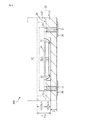
図1に示す従来の半導体パッケージ10は、シリコン基板12のキャビティ14内に接着層15を介して電子装置チップ16を搭載し、キャビティ14の開口を蓋18で気密封止し、キャビティ14の内部を不活性ガスで置換してある。キャビティ14の底面には配線パターン20が形成されており、ワイヤボンディング22により電子装置チップ16の電極17と接続されている。配線パターン20は貫通電極24を介して、搭載基板との接続用の裏面配線26へ引き出されている。
A
各部の寸法関係は、典型的には下記のようになる。 The dimensional relationship of each part is typically as follows.
例えばシリコン基板12として8インチウェーハ市販規格品を用いた場合、規格厚さ725μmであるが、裏面は梨地状であり使用に当って鏡面処理が必要で、そのための研磨代は50μm以上であるため、実際に用いる状態でのシリコン基板12の厚さXは例えば675μm以下となる。
For example, when a commercially available standard product of an 8-inch wafer is used as the
キャビティ14の底部は機械的な強度を確保するために例えば厚さZとして200μmとする。
The bottom of the
その結果、キャビティ14としての空間の高さYは475μm以下となる(Y=X−Z≦675−200=475)。
As a result, the height Y of the space as the
更に、ワイヤボンディング22を可能とするために電子装置チップ16上方の高さWとして150μmが、チップ実装用はんだ+メタル厚さの合計Tとして25μmが、それぞれ必要であるとすると、キャビティ14内に実際に収容可能なチップ16の高さHは300μm以下となる(H=Y−W−T≦475−150−25=300)。
Further, in order to enable
このように、従来のキャビティ内搭載に際しては搭載チップの許容高さが非常に限定されていた。 As described above, the allowable height of the mounting chip is very limited when mounting in the conventional cavity.
本発明は、市販シリコン基板の規格厚さによるチップ搭載高さの限界を超えて、シリコン基板のキャビティ内に電子装置チップを搭載した半導体パッケージを提供することを目的とする。 An object of the present invention is to provide a semiconductor package in which an electronic device chip is mounted in a cavity of a silicon substrate exceeding the limit of the chip mounting height due to the standard thickness of a commercially available silicon substrate.
上記の目的を達成するために、本発明によれば、複数枚のシリコン基板を貼り合せて成るシリコン基板積層体のキャビティ内に電子装置チップを搭載したことを特徴とする半導体パッケージが提供される。 In order to achieve the above object, according to the present invention, there is provided a semiconductor package characterized in that an electronic device chip is mounted in a cavity of a silicon substrate laminate formed by bonding a plurality of silicon substrates. .
本発明によれば、複数枚のシリコン基板を貼り合せて成るシリコン基板積層体にキャビティを設けたことにより、単独のシリコン基板の規格厚さに限定されずにキャビティ高さを達成することができ、従来は搭載不可能であった高さの電子装置チップあるいは電子装置チップスタックをキャビティに収容して搭載することができる。 According to the present invention, by providing a cavity in a silicon substrate laminate formed by bonding a plurality of silicon substrates, the cavity height can be achieved without being limited to the standard thickness of a single silicon substrate. The electronic device chip or the electronic device chip stack having a height that could not be mounted conventionally can be accommodated and mounted in the cavity.
〔実施形態1〕
図2に示す半導体パッケージ100は、貫通穴としてのキャビティ14Aを開口した窓枠状のシリコン基板12Aを別のシリコン基板12B上に接合面30で貼り合せてシリコン基板積層体120とした構成である。なお、図1中の部材に対応する部材には図1と同じ参照番号を付した。対応部材が複数ある場合には、参照番号の末尾にアルファベットを追加して区別した。また、シリコン基板表面の酸化絶縁膜、電子装置チップの電極など、本発明の理解に不要な細部は図示を省略し、説明を簡素かつ明瞭にした。
Embodiment 1
The
本実施形態においては、窓枠状の貫通キャビティ14Aを開口したシリコン基板12Aの厚さ全体をキャビティ14Aの高さYとして利用できる。例えば、シリコン基板12Aとして図1と同じく8インチウェーハ市販規格品を用いた場合、研磨後厚さの最大値675μmをそのままキャビティ14Aの高さYの最大値として利用できる。
In the present embodiment, the entire thickness of the
下側のシリコン基板12Bの上面が規定するキャビティ14Aの底面上に、接着層15を介して電子装置チップ16Bが搭載され、更にその上に接着層15を介して異種あるいは同種の電子装置チップ16Aが搭載されて、2個の電子装置チップ16A/16Bから成るスタックとして搭載されている。
An
キャビティ底面上には配線パターン20が形成されており、下側のシリコン基板12Bを貫通する貫通電極24を介して、搭載基板との接続用の裏面配線26へ引き出されている。
A
電子装置チップ16A、16Bと配線パターン20とはワイヤボンディング22A、22Bによりそれぞれ接続され、電子装置チップ16Aと16Bとはワイヤボンディング22Cにより接続されている。
The
図示の例では、2個の電子装置チップ16A/16Bのスタックを搭載した構成を示したが、1個の大きい高さの電子装置チップを搭載することもできる。もちろん、本発明の目的からは逸れるが、3個以上の小さい高さの電子装置チップを搭載することもできる。
In the illustrated example, a configuration in which a stack of two
2個のシリコン基板12A/12Bの接合部30における接合は、気密性を確保できる接合方法で行なうことが望ましく、従来から知られているシリコン同士の直接接合、接着剤接合、ろうまたははんだ接合などの接合方法を適用できる。
The bonding of the two
蓋18は、ガラス、プラスチック、シリコン、金属など気密性を確保できる種々の材質を用いることができ、透明性を要する場合には、ガラス、プラスチックなどを用いる。例えば蓋18としてガラスを用いた場合には、シリコン基板12Aとの接合は陽極接合により行なうことが望ましい。もちろん、接着剤接合など、他の気密性接合であってもよい。
The
〔実施形態2〕
図3に示す半導体パッケージ200は、貫通穴としてのキャビティ14Aを開口した窓枠状のシリコン基板12Aを、有底穴としてのキャビティ14Bを掘り込んだ別のシリコン基板12B上に接合面30で貼り合せてシリコン基板積層体120とした構成である。図1中の部材に対応する部材には図1と同じ参照番号を付した。対応部材が複数ある場合には、参照番号の末尾にアルファベットを追加して区別した。
[Embodiment 2]
In the
本実施形態においては、シリコン基板12Aの全厚に対応する高さの窓枠状貫通キャビティ14Aと、シリコン基板12Bの有底キャビティ14Bとの合計高さを、キャビティ14の高さYとして利用できる。例えば、シリコン基板12A、12Bとして図1と同じく8インチウェーハ市販規格品を用いた場合、シリコン基板12Aについては研磨後厚さの最大値675μmをそのままキャビティ14Aの高さYAの最大値として利用でき、加えて、シリコン基板12Bについては底部厚さ200μmを675μmから差し引いた475μmをキャビティ14Bの高さYBの最大値として利用できる。したがって、キャビティ14の高さYは、キャビティ14Aの高さYAとキャビティ14Bの高さYBとの合計として、1150μmを最大値として利用できる(Y=YA+YB≦675+475=1150)。
In the present embodiment, utilizing a window frame-shaped through
下側のシリコン基板12Bで構成するキャビティ14の底面上に、配線パターン20が形成され、その上に電子装置チップ16Bがバンプ19を介してフリップチップ接続により搭載され、更にその上に異種あるいは同種の電子装置チップ16Aが接着剤15を介して搭載されて、2個の電子装置チップ16A/16Bから成るスタックとして搭載されている。
A
電子装置チップ16Aはワイヤボンディング22により配線パターン20と接続されている。
The
キャビティ底面上に形成された配線パターン20は、下側のシリコン基板12Bを貫通する貫通電極24を介して、搭載基板との接続用の裏面配線26へ引き出されている。
The
電子装置チップの搭載個数、シリコン基板同士の接合方法、蓋の材質および蓋とシリコン基板との接合方法については、実施形態1と同様の選択肢が可能である。 With respect to the number of electronic device chips mounted, the bonding method between silicon substrates, the material of the lid, and the bonding method between the lid and the silicon substrate, the same options as in the first embodiment are possible.
〔実施形態3〕
図4に示す半導体パッケージ300は、貫通穴としてのキャビティ14Aを開口した窓枠状のシリコン基板12Aを、有底穴としてのキャビティ14Bを掘り込んだ別のシリコン基板12B上に接合面30で貼り合せてシリコン基板積層体120とした構成である。図1中の部材に対応する部材には図1と同じ参照番号を付した。対応部材が複数ある場合には、参照番号の末尾にアルファベットを追加して区別した。
[Embodiment 3]
In a
本実施形態においては、実施形態2と同様に、シリコン基板12Aの全厚に対応する高さの貫通キャビティ14Aと、シリコン基板12Bの有底キャビティ14Bとの合計高さを、キャビティ14の高さYとして利用できる。例えば、シリコン基板12A、12Bとして図1と同じく8インチウェーハ市販規格品を用いた場合、シリコン基板12Aについては研磨後厚さの最大値675μmをそのままキャビティ14Aの高さYAの最大値として利用でき、加えて、シリコン基板12Bについては底部厚さ200μmを675μmから差し引いた475μmをキャビティ14Bの高さYBの最大値として利用できる。したがって、キャビティ14の高さYは、キャビティ14Aの高さYAとキャビティ14Bの高さYBとの合計として、1150μmを最大値として利用できる(Y=YA+YB≦675+475=1150)。
In the present embodiment, similarly to
電子装置チップ16A上に異種または同種の電子装置チップ16Bを接着剤層15を介して搭載し、両チップ16A/16Bをワイヤボンディング22で接続してスタックとする。このスタックを裏返して、前者の電子装置チップ16Aのバンプ19を介して、下側のシリコン基板12Bの貫通電極24の上端にフリップチップ接続してある。これにより、電子装置チップ16Aのバンプ19は、搭載基板との接続用の裏面配線26へ引き出されている。
A different type or the same type of
電子装置チップの搭載個数、シリコン基板同士の接合方法、蓋の材質および蓋とシリコン基板との接合方法については、実施形態1と同様の選択肢が可能である。 With respect to the number of electronic device chips mounted, the bonding method between silicon substrates, the material of the lid, and the bonding method between the lid and the silicon substrate, the same options as in the first embodiment are possible.
〔実施形態4〕
図5に示す半導体パッケージ400は、有底穴としてのキャビティ14Aを掘り込んだシリコン基板12Aを、テーパ付き貫通穴としてのキャビティ14Bを開口した窓枠状のシリコン基板12B上に、シリコン基板12Aの底部裏面を接合面30として貼り合せてシリコン基板積層体120とした構成である。すなわち、キャビティ12Aの底部を境界領域として、キャビティ12A、12Bがそれぞれ上下に開口した構造である。図1中の部材に対応する部材には図1と同じ参照番号を付した。対応部材が複数ある場合には、参照番号の末尾にアルファベットまたはアルファベットと数字を追加して区別した。
[Embodiment 4]
In a
本実施形態においては、上側のシリコン基板12Aについては図1の従来構造と同じく、有底キャビティ14Aは市販ウェーハの研磨後厚さ(675μm:8インチウェーハの場合。以下同様)から底部の厚さZを差し引いた最大高さ(475μm)であるが、シリコン基板12Bについては図2の実施形態1および図4の実施形態3と同じく、窓枠状貫通キャビティ14Bは市販ウェーハの研磨後厚さ(675μm)全てを最大高さとして利用できる。
In the present embodiment, as for the
上側のキャビティ14A内では、キャビティ14Aの底面上に接着剤層15を介して電子装置チップ16A2を搭載し、その上に接着剤層15を介して異種または同種の電子装置チップ16A1を搭載してスタックとする。各電子装置チップ16A1、16A2はワイヤボンディング22A1、22A2によりそれぞれキャビティ14Aの底面上の配線パターン20Aに接続されている。上側キャビティ14Aはシリコン基板12Aに接合した蓋18により気密封止され、内部は不活性ガス置換または真空状態にされている。
In the
下側のキャビティ14B内では、シリコン基板12Aの裏面により構成された底面上に、接着剤層15を介して電子装置チップ16B2を搭載し、その上に接着剤層15を介して異種または同種の電子装置チップ16B1を搭載してスタックとする。各電子装置チップ16B1、16B2はワイヤボンディング22B1、22B2によりそれぞれキャビティ14Bの底面上の配線パターン20Bに接続されている。下側キャビティ14B内は実際にはモールド樹脂28で充填されている。下側キャビティ14Bの周縁ではテーパ配線26Tにより、配線パターン20Bが搭載基板との接続用の裏面配線26まで引き出されている。
In the lower cavity 14B, an electronic device chip 16B2 is mounted on the bottom surface constituted by the back surface of the
電子装置チップの搭載個数、シリコン基板同士の接合方法、蓋の材質および蓋とシリコン基板との接合方法については、実施形態1と同様の選択肢が可能である。 With respect to the number of electronic device chips mounted, the bonding method between silicon substrates, the material of the lid, and the bonding method between the lid and the silicon substrate, the same options as in the first embodiment are possible.
〔実施形態5〕
図6に示す半導体パッケージ500は、貫通穴としてのキャビティ14Aを掘り込んだ窓枠状のシリコン基板12Aを、有底穴としてのキャビティ14Bを開口したシリコン基板12B上に、シリコン基板12Bの底部裏面を接合面30として貼り合せてシリコン基板積層体120とした構成である。すなわち、キャビティ12Bの底部を境界領域として、キャビティ12A、12Bがそれぞれ上下に開口した構造である。図1中の部材に対応する部材には図1と同じ参照番号を付した。対応部材が複数ある場合には、参照番号の末尾にアルファベットまたはアルファベットと数字を追加して区別した。
[Embodiment 5]
A
本実施形態においては、上側のシリコン基板12Aについては、実施形態1および図4の実施形態3と同じく、貫通キャビティ14Aは市販ウェーハの研磨後厚さ(675μm)全てを最大高さとして利用でき、シリコン基板12Bについては図1の従来構造と同じく、有底キャビティ14Bは市販ウェーハの研磨後厚さ(675μm:8インチウェーハの場合。以下同様)から底部の厚さZを差し引いた最大高さ(475μm)である。
In the present embodiment, for the
上側のキャビティ14A内では、シリコン基板12Bの裏面により構成された底面上に接着剤層15を介して電子装置チップ16A2を搭載し、その上に接着剤層15を介して異種または同種の電子装置チップ16A1を搭載してスタックとする。各電子装置チップ16A1、16A2はワイヤボンディング22A1、22A2によりそれぞれキャビティ14Aの底面上の配線パターン20Aに接続されている。上側キャビティ14Aはシリコン基板12Aに接合した蓋18により気密封止され、内部は不活性ガス置換または真空状態にされている。
In the
下側のキャビティ14B内では、キャビティ14Bの底面上に、接着剤層15を介して電子装置チップ16B2を搭載し、その上に接着剤層15を介して異種または同種の電子装置チップ16B1を搭載してスタックとする。各電子装置チップ16B1、16B2はワイヤボンディング22B1、22B2によりそれぞれキャビティ14Bの底面上の配線パターン20Bに接続されている。下側キャビティ14B内は実際にはモールド樹脂28で充填されている。下側キャビティ14Bの周縁ではテーパ配線26Tにより、配線パターン20Bが搭載基板との接続用の裏面配線26まで引き出されている。
In the lower cavity 14B, an electronic device chip 16B2 is mounted on the bottom surface of the cavity 14B via an
上側のキャビティ14A内の配線パターン20Aと、下側のキャビティ14B内の配線パターン20Bとは、下側のシリコン基板12Bの底部を貫通するビア23により接続されている。
The
電子装置チップの搭載個数、シリコン基板同士の接合方法、蓋の材質および蓋とシリコン基板との接合方法については、実施形態1と同様の選択肢が可能である。 With respect to the number of electronic device chips mounted, the bonding method between silicon substrates, the material of the lid, and the bonding method between the lid and the silicon substrate, the same options as in the first embodiment are possible.
本発明によれば、市販シリコン基板の規格厚さによるチップ搭載高さの限界を超えて、シリコン基板のキャビティ内に電子装置チップを搭載した半導体パッケージが提供される。 According to the present invention, there is provided a semiconductor package in which an electronic device chip is mounted in a cavity of a silicon substrate exceeding the limit of the chip mounting height due to the standard thickness of a commercially available silicon substrate.
100、200、300、400、500 半導体パッケージ
12A、12B シリコン基板
120 シリコン基板積層体
14、14A、14B キャビティ
16A、16A1、16A2、16B、16B1、16B2 電子装置チップ
18 蓋
20 配線パターン
22、22A、22A1、22A2、22B、22B1、22B2、22C ワイヤボンディング
23 ビア
24 貫通電極
26 裏面配線
28 モールド樹脂
30 接合部
100, 200, 300, 400, 500
Claims (4)
有底穴である第2のキャビティおよび貫通電極を有し、前記第2のキャビティの底部裏面が前記第1のキャビティに向くように前記第1のシリコン基板と接合される第2のシリコン基板と、
前記第1のキャビティおよび前記第2のキャビティ内に収容される複数の電子装置チップと、
を備えることを特徴とする半導体パッケージ。 A first silicon substrate having a first cavity that is a through hole;
A second silicon substrate that has a second cavity that is a bottomed hole and a through electrode, and is joined to the first silicon substrate so that a bottom back surface of the second cavity faces the first cavity; ,
A plurality of electronic device chips housed in the first cavity and the second cavity;
A semiconductor package comprising:
Priority Applications (4)
| Application Number | Priority Date | Filing Date | Title |
|---|---|---|---|
| JP2007288907A JP4912275B2 (en) | 2007-11-06 | 2007-11-06 | Semiconductor package |
| EP08168216A EP2058872A2 (en) | 2007-11-06 | 2008-11-03 | Semiconductor package |
| US12/265,203 US7960820B2 (en) | 2007-11-06 | 2008-11-05 | Semiconductor package |
| TW097142608A TW200921860A (en) | 2007-11-06 | 2008-11-05 | Semiconductor package |
Applications Claiming Priority (1)
| Application Number | Priority Date | Filing Date | Title |
|---|---|---|---|
| JP2007288907A JP4912275B2 (en) | 2007-11-06 | 2007-11-06 | Semiconductor package |
Publications (3)
| Publication Number | Publication Date |
|---|---|
| JP2009117611A JP2009117611A (en) | 2009-05-28 |
| JP2009117611A5 JP2009117611A5 (en) | 2010-11-11 |
| JP4912275B2 true JP4912275B2 (en) | 2012-04-11 |
Family
ID=40230534
Family Applications (1)
| Application Number | Title | Priority Date | Filing Date |
|---|---|---|---|
| JP2007288907A Active JP4912275B2 (en) | 2007-11-06 | 2007-11-06 | Semiconductor package |
Country Status (4)
| Country | Link |
|---|---|
| US (1) | US7960820B2 (en) |
| EP (1) | EP2058872A2 (en) |
| JP (1) | JP4912275B2 (en) |
| TW (1) | TW200921860A (en) |
Families Citing this family (27)
| Publication number | Priority date | Publication date | Assignee | Title |
|---|---|---|---|---|
| KR100836663B1 (en) * | 2006-02-16 | 2008-06-10 | 삼성전기주식회사 | Package on package with cavity and Method for manufacturing thereof |
| DE102009022901A1 (en) * | 2009-05-27 | 2010-12-02 | Osram Opto Semiconductors Gmbh | Optoelectronic module and method for producing an optoelectronic module |
| JP2011023709A (en) * | 2009-06-18 | 2011-02-03 | Shinko Electric Ind Co Ltd | Semiconductor device and method of manufacturing the same |
| JP5208871B2 (en) * | 2009-07-13 | 2013-06-12 | 浜松ホトニクス株式会社 | Photodetector |
| JP5100715B2 (en) * | 2009-07-13 | 2012-12-19 | 株式会社東芝 | Semiconductor device and manufacturing method of semiconductor device |
| TWI453957B (en) * | 2010-05-24 | 2014-09-21 | Advanced Optoelectronic Tech | Light emitting diode package |
| TWI406435B (en) * | 2010-08-06 | 2013-08-21 | Advanced Optoelectronic Tech | Method for manufacturing led |
| US9443834B2 (en) * | 2010-09-02 | 2016-09-13 | Micron Technology, Inc. | Back-to-back solid state lighting devices and associated methods |
| JP2012119601A (en) * | 2010-12-03 | 2012-06-21 | Nec Corp | Interposer and semiconductor device |
| US9013011B1 (en) * | 2011-03-11 | 2015-04-21 | Amkor Technology, Inc. | Stacked and staggered die MEMS package and method |
| US9105635B2 (en) * | 2013-03-13 | 2015-08-11 | Intel Corporation | Stubby pads for channel cross-talk reduction |
| WO2015136998A1 (en) * | 2014-03-10 | 2015-09-17 | 三菱重工業株式会社 | Multi-chip module, on-board computer, sensor interface substrate, and multi-chip module manufacturing method |
| JP2016004888A (en) * | 2014-06-17 | 2016-01-12 | イビデン株式会社 | Printed wiring board and method for manufacturing printed wiring board |
| JP6663167B2 (en) * | 2015-03-18 | 2020-03-11 | 浜松ホトニクス株式会社 | Photodetector |
| US11211305B2 (en) | 2016-04-01 | 2021-12-28 | Texas Instruments Incorporated | Apparatus and method to support thermal management of semiconductor-based components |
| US10861796B2 (en) * | 2016-05-10 | 2020-12-08 | Texas Instruments Incorporated | Floating die package |
| US10179730B2 (en) | 2016-12-08 | 2019-01-15 | Texas Instruments Incorporated | Electronic sensors with sensor die in package structure cavity |
| US9929110B1 (en) | 2016-12-30 | 2018-03-27 | Texas Instruments Incorporated | Integrated circuit wave device and method |
| US10074639B2 (en) | 2016-12-30 | 2018-09-11 | Texas Instruments Incorporated | Isolator integrated circuits with package structure cavity and fabrication methods |
| US10411150B2 (en) | 2016-12-30 | 2019-09-10 | Texas Instruments Incorporated | Optical isolation systems and circuits and photon detectors with extended lateral P-N junctions |
| US10121847B2 (en) | 2017-03-17 | 2018-11-06 | Texas Instruments Incorporated | Galvanic isolation device |
| JP6993220B2 (en) * | 2017-12-26 | 2022-01-13 | 京セラ株式会社 | Electronic component storage packages, electronic devices and electronic modules |
| DE102018100946A1 (en) * | 2018-01-17 | 2019-07-18 | Osram Opto Semiconductors Gmbh | COMPONENT AND METHOD FOR PRODUCING A COMPONENT |
| KR20210007217A (en) * | 2019-07-10 | 2021-01-20 | 삼성전자주식회사 | An electronic device including an interposer |
| SG10201908828WA (en) | 2019-09-23 | 2021-04-29 | Apple Inc | Embedded Packaging Concepts for Integration of ASICs and Optical Components |
| US11942386B2 (en) * | 2020-08-24 | 2024-03-26 | Texas Instruments Incorporated | Electronic devices in semiconductor package cavities |
| US20230213715A1 (en) * | 2022-01-03 | 2023-07-06 | Apple Inc. | Technologies for Increased Volumetric and Functional Efficiencies of Optical Packages |
Family Cites Families (10)
| Publication number | Priority date | Publication date | Assignee | Title |
|---|---|---|---|---|
| JPS5875859A (en) * | 1981-10-30 | 1983-05-07 | Fujitsu Ltd | Semiconductor device |
| US5422435A (en) * | 1992-05-22 | 1995-06-06 | National Semiconductor Corporation | Stacked multi-chip modules and method of manufacturing |
| US6343019B1 (en) * | 1997-12-22 | 2002-01-29 | Micron Technology, Inc. | Apparatus and method of stacking die on a substrate |
| US20040038442A1 (en) * | 2002-08-26 | 2004-02-26 | Kinsman Larry D. | Optically interactive device packages and methods of assembly |
| JP2004296613A (en) * | 2003-03-26 | 2004-10-21 | Renesas Technology Corp | Semiconductor device |
| JP2006186357A (en) * | 2003-10-03 | 2006-07-13 | Matsushita Electric Works Ltd | Sensor device and its manufacturing method |
| JP4692260B2 (en) * | 2005-12-12 | 2011-06-01 | 株式会社デンソー | Semiconductor dynamic quantity sensor device and manufacturing method thereof |
| JP4996101B2 (en) | 2006-02-02 | 2012-08-08 | 新光電気工業株式会社 | Semiconductor device and manufacturing method of semiconductor device |
| JP2007287967A (en) * | 2006-04-18 | 2007-11-01 | Shinko Electric Ind Co Ltd | Electronic-component apparatus |
| JP4933934B2 (en) * | 2007-03-28 | 2012-05-16 | ラピスセミコンダクタ株式会社 | Semiconductor device and manufacturing method of semiconductor device |
-
2007
- 2007-11-06 JP JP2007288907A patent/JP4912275B2/en active Active
-
2008
- 2008-11-03 EP EP08168216A patent/EP2058872A2/en not_active Withdrawn
- 2008-11-05 TW TW097142608A patent/TW200921860A/en unknown
- 2008-11-05 US US12/265,203 patent/US7960820B2/en active Active
Also Published As
| Publication number | Publication date |
|---|---|
| US7960820B2 (en) | 2011-06-14 |
| EP2058872A2 (en) | 2009-05-13 |
| TW200921860A (en) | 2009-05-16 |
| US20090115049A1 (en) | 2009-05-07 |
| JP2009117611A (en) | 2009-05-28 |
Similar Documents
| Publication | Publication Date | Title |
|---|---|---|
| JP4912275B2 (en) | Semiconductor package | |
| US9543735B2 (en) | Optoelectronic packages having through-channels for routing and vacuum | |
| US20160291269A1 (en) | Photonic integrated circuit chip packaging | |
| JP5026038B2 (en) | Electronic component equipment | |
| US9796580B2 (en) | CMOS-MEMS-CMOS platform | |
| TWI333264B (en) | Packaging structure and method of mems microphone | |
| US20060211177A1 (en) | Structure and process for packaging RF MEMS and other devices | |
| JP5610156B2 (en) | Photoelectric conversion module and method for manufacturing photoelectric conversion module | |
| TW200525769A (en) | Method and system for hermetically sealing packages for optics | |
| US7829993B2 (en) | Semiconductor apparatus | |
| US20220157684A1 (en) | Hermetically sealed glass enclosure | |
| JP2022549707A (en) | sealed glass enclosure | |
| JP2005019966A (en) | Semiconductor device and method of manufacturing the same | |
| WO2005105661A1 (en) | Techniques for providing a structure with through-holes that may be used in a sub-assembly for micro-components | |
| JP2003107301A (en) | Module for optical communication | |
| KR101470946B1 (en) | hermetic package of Semiconductor chip and thereof. | |
| JP2008034515A (en) | Electronic apparatus and package | |
| JP2007042786A (en) | Micro device and its packaging method | |
| JP2008147243A (en) | Hermetic sealing apparatus | |
| JP2011216712A (en) | Electronic device | |
| JP2013026506A (en) | Electronic component storing package and electronic apparatus | |
| CN110104606A (en) | A kind of encapsulating structure of MEMS infrared sensor | |
| KR100902913B1 (en) | Laminated semiconductor package and method for manufacturing the same | |
| WO2014020648A1 (en) | Electronic device | |
| JP2018084439A (en) | package |
Legal Events
| Date | Code | Title | Description |
|---|---|---|---|
| A521 | Request for written amendment filed |
Free format text: JAPANESE INTERMEDIATE CODE: A523 Effective date: 20100914 |
|
| A621 | Written request for application examination |
Free format text: JAPANESE INTERMEDIATE CODE: A621 Effective date: 20100914 |
|
| A977 | Report on retrieval |
Free format text: JAPANESE INTERMEDIATE CODE: A971007 Effective date: 20110922 |
|
| A131 | Notification of reasons for refusal |
Free format text: JAPANESE INTERMEDIATE CODE: A131 Effective date: 20111004 |
|
| A521 | Request for written amendment filed |
Free format text: JAPANESE INTERMEDIATE CODE: A523 Effective date: 20111202 |
|
| TRDD | Decision of grant or rejection written | ||
| A01 | Written decision to grant a patent or to grant a registration (utility model) |
Free format text: JAPANESE INTERMEDIATE CODE: A01 Effective date: 20111220 |
|
| A01 | Written decision to grant a patent or to grant a registration (utility model) |
Free format text: JAPANESE INTERMEDIATE CODE: A01 |
|
| A61 | First payment of annual fees (during grant procedure) |
Free format text: JAPANESE INTERMEDIATE CODE: A61 Effective date: 20120117 |
|
| R150 | Certificate of patent or registration of utility model |
Ref document number: 4912275 Country of ref document: JP Free format text: JAPANESE INTERMEDIATE CODE: R150 Free format text: JAPANESE INTERMEDIATE CODE: R150 |
|
| FPAY | Renewal fee payment (event date is renewal date of database) |
Free format text: PAYMENT UNTIL: 20150127 Year of fee payment: 3 |