JP4996101B2 - Semiconductor device and manufacturing method of semiconductor device - Google Patents
Semiconductor device and manufacturing method of semiconductor device Download PDFInfo
- Publication number
- JP4996101B2 JP4996101B2 JP2006025649A JP2006025649A JP4996101B2 JP 4996101 B2 JP4996101 B2 JP 4996101B2 JP 2006025649 A JP2006025649 A JP 2006025649A JP 2006025649 A JP2006025649 A JP 2006025649A JP 4996101 B2 JP4996101 B2 JP 4996101B2
- Authority
- JP
- Japan
- Prior art keywords
- light
- semiconductor device
- substrate
- cover
- film
- Prior art date
- Legal status (The legal status is an assumption and is not a legal conclusion. Google has not performed a legal analysis and makes no representation as to the accuracy of the status listed.)
- Expired - Fee Related
Links
Images


Classifications
-
- H—ELECTRICITY
- H01—ELECTRIC ELEMENTS
- H01L—SEMICONDUCTOR DEVICES NOT COVERED BY CLASS H10
- H01L33/00—Semiconductor devices with at least one potential-jump barrier or surface barrier specially adapted for light emission; Processes or apparatus specially adapted for the manufacture or treatment thereof or of parts thereof; Details thereof
- H01L33/48—Semiconductor devices with at least one potential-jump barrier or surface barrier specially adapted for light emission; Processes or apparatus specially adapted for the manufacture or treatment thereof or of parts thereof; Details thereof characterised by the semiconductor body packages
- H01L33/58—Optical field-shaping elements
-
- H—ELECTRICITY
- H01—ELECTRIC ELEMENTS
- H01L—SEMICONDUCTOR DEVICES NOT COVERED BY CLASS H10
- H01L24/00—Arrangements for connecting or disconnecting semiconductor or solid-state bodies; Methods or apparatus related thereto
- H01L24/93—Batch processes
- H01L24/95—Batch processes at chip-level, i.e. with connecting carried out on a plurality of singulated devices, i.e. on diced chips
- H01L24/97—Batch processes at chip-level, i.e. with connecting carried out on a plurality of singulated devices, i.e. on diced chips the devices being connected to a common substrate, e.g. interposer, said common substrate being separable into individual assemblies after connecting
-
- H—ELECTRICITY
- H01—ELECTRIC ELEMENTS
- H01L—SEMICONDUCTOR DEVICES NOT COVERED BY CLASS H10
- H01L2224/00—Indexing scheme for arrangements for connecting or disconnecting semiconductor or solid-state bodies and methods related thereto as covered by H01L24/00
- H01L2224/01—Means for bonding being attached to, or being formed on, the surface to be connected, e.g. chip-to-package, die-attach, "first-level" interconnects; Manufacturing methods related thereto
- H01L2224/10—Bump connectors; Manufacturing methods related thereto
- H01L2224/12—Structure, shape, material or disposition of the bump connectors prior to the connecting process
- H01L2224/13—Structure, shape, material or disposition of the bump connectors prior to the connecting process of an individual bump connector
-
- H—ELECTRICITY
- H01—ELECTRIC ELEMENTS
- H01L—SEMICONDUCTOR DEVICES NOT COVERED BY CLASS H10
- H01L2224/00—Indexing scheme for arrangements for connecting or disconnecting semiconductor or solid-state bodies and methods related thereto as covered by H01L24/00
- H01L2224/01—Means for bonding being attached to, or being formed on, the surface to be connected, e.g. chip-to-package, die-attach, "first-level" interconnects; Manufacturing methods related thereto
- H01L2224/42—Wire connectors; Manufacturing methods related thereto
- H01L2224/47—Structure, shape, material or disposition of the wire connectors after the connecting process
- H01L2224/48—Structure, shape, material or disposition of the wire connectors after the connecting process of an individual wire connector
- H01L2224/4805—Shape
- H01L2224/4809—Loop shape
- H01L2224/48091—Arched
-
- H—ELECTRICITY
- H01—ELECTRIC ELEMENTS
- H01L—SEMICONDUCTOR DEVICES NOT COVERED BY CLASS H10
- H01L2924/00—Indexing scheme for arrangements or methods for connecting or disconnecting semiconductor or solid-state bodies as covered by H01L24/00
- H01L2924/10—Details of semiconductor or other solid state devices to be connected
- H01L2924/11—Device type
- H01L2924/12—Passive devices, e.g. 2 terminal devices
- H01L2924/1204—Optical Diode
- H01L2924/12041—LED
-
- H—ELECTRICITY
- H01—ELECTRIC ELEMENTS
- H01L—SEMICONDUCTOR DEVICES NOT COVERED BY CLASS H10
- H01L33/00—Semiconductor devices with at least one potential-jump barrier or surface barrier specially adapted for light emission; Processes or apparatus specially adapted for the manufacture or treatment thereof or of parts thereof; Details thereof
- H01L33/44—Semiconductor devices with at least one potential-jump barrier or surface barrier specially adapted for light emission; Processes or apparatus specially adapted for the manufacture or treatment thereof or of parts thereof; Details thereof characterised by the coatings, e.g. passivation layer or anti-reflective coating
-
- H—ELECTRICITY
- H01—ELECTRIC ELEMENTS
- H01L—SEMICONDUCTOR DEVICES NOT COVERED BY CLASS H10
- H01L33/00—Semiconductor devices with at least one potential-jump barrier or surface barrier specially adapted for light emission; Processes or apparatus specially adapted for the manufacture or treatment thereof or of parts thereof; Details thereof
- H01L33/48—Semiconductor devices with at least one potential-jump barrier or surface barrier specially adapted for light emission; Processes or apparatus specially adapted for the manufacture or treatment thereof or of parts thereof; Details thereof characterised by the semiconductor body packages
- H01L33/50—Wavelength conversion elements
- H01L33/507—Wavelength conversion elements the elements being in intimate contact with parts other than the semiconductor body or integrated with parts other than the semiconductor body
-
- H—ELECTRICITY
- H01—ELECTRIC ELEMENTS
- H01L—SEMICONDUCTOR DEVICES NOT COVERED BY CLASS H10
- H01L33/00—Semiconductor devices with at least one potential-jump barrier or surface barrier specially adapted for light emission; Processes or apparatus specially adapted for the manufacture or treatment thereof or of parts thereof; Details thereof
- H01L33/48—Semiconductor devices with at least one potential-jump barrier or surface barrier specially adapted for light emission; Processes or apparatus specially adapted for the manufacture or treatment thereof or of parts thereof; Details thereof characterised by the semiconductor body packages
- H01L33/58—Optical field-shaping elements
- H01L33/60—Reflective elements
Description
本発明は半導体装置及びその製造方法に係り、特に基板に発光素子または受光素子よりなる光機能素子が実装されてなる半導体装置及びその製造方法に関する。 The present invention relates to a semiconductor device and a manufacturing method thereof, and more particularly, to a semiconductor device in which an optical functional element including a light emitting element or a light receiving element is mounted on a substrate, and a manufacturing method thereof.
発光素子が基板に実装されてなる半導体装置には、様々な形状のものが提案されているが、例えば発光素子がLED(light emitting diode)などの場合、その発光色の種類は限られている。そのため、所望の発光色を得るために、LEDの発光に対応して発光する蛍光体を用いて、LEDの発光と蛍光体の発光の混色を用いる場合がある。 Semiconductor devices having a light emitting element mounted on a substrate have been proposed in various shapes. For example, when the light emitting element is an LED (light emitting diode) or the like, the types of emission colors are limited. . Therefore, in order to obtain a desired emission color, a phosphor that emits light corresponding to the emission of the LED may be used, and a mixed color of the emission of the LED and the emission of the phosphor may be used.
従来の発光素子が実装された半導体装置としては、例えば、基板の凹部に発光素子を実装し、凹部の上部開口をガラスなどの光学部材(ガラス)により封止し、光学部材の下面に形成された蛍光部材が発光素子からの光を受けて発光することで光学部材から出射される光強度を高めるように構成されたものがある(例えば、特許文献1を参照)。
しかしながら、上記従来の半導体装置では、発光素子からの光が基板の凹部を覆う光学部材を透過して出射される過程で屈折率の異なる境界面を通過する際、例えば、屈折率の大きい光学部材(屈折率=1.5)から屈折率の小さい空気(屈折率=1.0)に進行する場合に境界面に対する光の入射角によって全反射が発生してしまい、光学部材を透過する光量が減少して光強度が低下するという問題があった。 However, in the conventional semiconductor device, when light from the light emitting element passes through the boundary surface having a different refractive index in the process of being transmitted through the optical member covering the concave portion of the substrate and emitted, for example, an optical member having a large refractive index. When traveling from (refractive index = 1.5) to air having a low refractive index (refractive index = 1.0), total reflection occurs due to the incident angle of light with respect to the boundary surface, and the amount of light transmitted through the optical member is reduced. There was a problem that the light intensity decreased due to a decrease.
また、光の全反射は、光が屈折率の大きい媒質から屈折率の小さい媒質へ進行する際に発生する現象であるので、発光素子の内部から外部に光が放射される際にも発生するおそれがある。このような場合には、発光素子の上面に向けて光を放射させる構成であるのに、発光素子の内部に全反射した光が発光素子の側面から放射されてしまい、本来の発光面である発光素子の上面からの光強度が低下するという問題もあった。 In addition, total reflection of light is a phenomenon that occurs when light travels from a medium with a high refractive index to a medium with a low refractive index, and thus also occurs when light is emitted from the inside of the light emitting element to the outside. There is a fear. In such a case, the light is emitted toward the upper surface of the light emitting element, but the light totally reflected inside the light emitting element is emitted from the side surface of the light emitting element, which is the original light emitting surface. There is also a problem that the light intensity from the upper surface of the light emitting element is lowered.
そこで、本発明では、上記の点に鑑み、上記問題を解決した半導体装置を提供することを統括的課題としている。 Therefore, in view of the above points, the present invention has a general object to provide a semiconductor device that solves the above problems.
上記課題を解決するため、本発明は以下のような手段を有する。 In order to solve the above problems, the present invention has the following means.
本発明は、基板に光機能素子が実装されてなる半導体装置であって、前記光機能素子上には光透過性を有するカバーが設置され、前記カバーの上面及び前記光機能素子の上面に光の反射を防止する光反射防止膜が形成され、前記カバーの下面に蛍光体膜が形成され、前記基板を貫通する貫通配線及び放熱配線が形成され、前記光機能素子の側面を囲むように、金属部材の表面に反射膜が形成されてなる、光を反射するリフレクタが配置され、前記リフレクタと前記放熱配線とが接続され、前記光機能素子は、バンプを介して前記貫通配線と電気的に接続され、前記放熱配線は、前記貫通配線の外側に設けられていることを特徴とする。 The present invention is a semiconductor device in which an optical functional element is mounted on a substrate, and a light-transmitting cover is installed on the optical functional element, and light is applied to the upper surface of the cover and the upper surface of the optical functional element. A light reflection preventing film for preventing reflection of light, a phosphor film is formed on the lower surface of the cover, a through wiring and a heat radiation wiring penetrating the substrate are formed, and so as to surround a side surface of the optical functional element , A reflector configured to reflect light is formed by forming a reflective film on the surface of the metal member, the reflector and the heat dissipation wiring are connected, and the optical functional element is electrically connected to the through wiring via a bump. It is connected, The said heat radiation wiring is provided in the outer side of the said penetration wiring, It is characterized by the above-mentioned.
前記光反射防止膜は、誘電体膜を多層コーティングして形成された透明膜であることを特徴とする。 The light reflection preventing film is a transparent film formed by coating a dielectric film in multiple layers.
前記光機能素子は、前記基板の凹部に実装され、前記凹部が前記カバーと前記基板が接合されて封止されていることを特徴とする。 The optical functional element is mounted in a concave portion of the substrate, and the concave portion is sealed by bonding the cover and the substrate.
また、本発明は、基板上に光機能素子を実装する工程と、前記光機能素子の上面に光反射防止膜を形成する工程と、前記基板上に設置された前記光機能素子を、光透過性を有するカバーを用いて封止する工程と、前記カバーの上面に光反射防止膜を形成する工程と、前記カバーの下面に蛍光体膜を形成する工程と、前記基板を貫通しバンプを介して前記光機能素子と電気的に接続される貫通配線を形成し、前記貫通配線の外側に前記基板を貫通する放熱配線を形成する工程と、前記光機能素子の側面を囲むように、金属部材の表面に反射膜が形成されてなる、光を反射するリフレクタを配置する工程と、前記リフレクタと前記放熱配線とを接続する工程と、を有することを特徴とする。 The present invention also includes a step of mounting an optical functional element on a substrate, a step of forming a light reflection preventing film on the upper surface of the optical functional element, and the optical functional element installed on the substrate. Sealing with a cover having a property, a step of forming an antireflection film on the upper surface of the cover, a step of forming a phosphor film on the lower surface of the cover, and through the substrate through bumps Forming a through-wiring electrically connected to the optical functional element , forming a heat dissipation wiring penetrating the substrate outside the through-wiring, and a metal member so as to surround a side surface of the optical functional element And a step of disposing a reflector that reflects light, and a step of connecting the reflector and the heat dissipating wiring.
前記基板は、前記光機能素子を実装する凹部が形成され、前記凹部の開口は、前記カバーを用いて封止されていることを特徴とする。 The substrate is provided with a recess for mounting the optical functional element, and the opening of the recess is sealed with the cover.
前記リフレクタの上端を前記カバーに接合する工程と、前記リフレクタの下端を前記光機能素子が載置された領域の周囲に接合して前記光機能素子が実装された空間を封止する工程と、を有することを特徴とする。 Bonding the upper end of the reflector to the cover, sealing the space where the optical functional element is mounted by bonding the lower end of the reflector around the area where the optical functional element is mounted; It is characterized by having.
本発明によれば、光機能素子上には光透過性を有するカバーが設置され、カバーの上面及び光機能素子の上面に光の反射を防止する光反射防止膜が形成され、カバーの下面に蛍光体膜が形成されているため、光機能素子から放射された光、または外部から入射された光の入射角が臨界角より大きい場合でも光を反射せずに光機能素子またはカバーを透過して進行することができるので、光機能素子から出射される光量、または外部から入射される光量が増大して発光、受光の光強度をより高めることが可能になる。また、基板を貫通する貫通配線及び放熱配線が形成され、光機能素子の側面を囲むように光を反射するリフレクタが配置され、リフレクタと放熱配線とが接続されているため、リフレクタの熱を放熱配線を介して基板の外側に逃がすことができるので、リフレクタの放熱性を良好に保つことができる。
According to the present invention, a light-transmitting cover is installed on the optical functional element, an antireflection film for preventing light reflection is formed on the upper surface of the cover and the upper surface of the optical functional element, and on the lower surface of the cover. Since the phosphor film is formed, even if the incident angle of the light emitted from the optical functional element or the light incident from the outside is larger than the critical angle, it does not reflect the light and passes through the optical functional element or the cover. Therefore, the amount of light emitted from the optical functional element or the amount of light incident from the outside increases, and the light intensity of light emission and reception can be further increased. Also, through-hole wiring and heat radiation wiring that penetrates the substrate are formed, a reflector that reflects light is arranged so as to surround the side surface of the optical functional element, and the reflector and heat radiation wiring are connected, so heat from the reflector is dissipated. Since it can escape to the outer side of a board | substrate via wiring, the heat dissipation of a reflector can be kept favorable.
以下、図面を参照して本発明を実施するための最良の形態について説明する。 The best mode for carrying out the present invention will be described below with reference to the drawings.
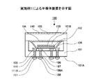
図1は、本発明の実施例1による半導体装置100を模式的に示した断面図である。図1を参照するに、半導体装置100は、例えばSiよりなる基板101に、光機能素子として、例えばLEDよりなる発光素子102が実装されてなる半導体装置である。発光素子102は、サファイア(Al2O3)を基材としてP層、N層、電極などが形成されており、その上面には、光の反射を防止する光反射防止膜130が形成されている。この光反射防止膜130は、例えば、誘電体膜を積層した多層反射防止膜(EBC:electron beam coating)、あるいはARコ−ティング(anti-reflective coating)と呼ばれる反射防止処理が施され、真空蒸着等により形成された透明な薄膜である。
FIG. 1 is a cross-sectional view schematically showing a
そのため、発光素子102の内部から外部に放射された光が発光素子102の上面(屈折率の境界面)を通過して空気中を進行する際に、屈折率の差によって光の全反射が起きることが防止される。
Therefore, when light radiated from the inside to the outside of the
尚、本実施例では、発光素子102が基板101に実装される構成について説明しているが、発光素子のみではなく、例えば、受光素子を実装した構成の半導体装置にも本発明を適用することができるのは、勿論である。その場合、光反射防止膜130は、外部から入射された光の反射を防止して受光される光強度を高めることができる。
In this embodiment, the configuration in which the
ここで、光の全反射が発生する原理について説明する。例えば、屈折率の異なる物質Aと物質Bとの境界では、光の屈折が発生することが知られている。そして、物質A中を進行する光が、境界面の入射点に到達した場合、当該入射点における境界面に対する法線と、入射光線が形成する角度を入射角と呼ぶ。この入射角を、ある角度以上とした場合には、光が透過せず、いわゆる全反射が生じる。このとき、全反射が生じる入射角は、臨界角または全反射の臨界角と呼ばれている。この臨界角は、物質A,Bの屈折率の比によって決まる角度である。 Here, the principle of total light reflection will be described. For example, it is known that light refraction occurs at the boundary between the substance A and the substance B having different refractive indexes. When light traveling in the substance A reaches the incident point on the boundary surface, the normal to the boundary surface at the incident point and the angle formed by the incident light beam are referred to as the incident angle. If this incident angle is greater than a certain angle, no light is transmitted and so-called total reflection occurs. At this time, the incident angle at which total reflection occurs is called the critical angle or the critical angle of total reflection. This critical angle is an angle determined by the ratio of the refractive indexes of the substances A and B.
物質Aの屈折率n1、物質Bの屈折率n2、臨界角θfとした場合、屈折率と臨界角との関係は、次式(1)のように表される。
Sinθf=n2/n1・・・(1)
この場合、全反射が生じるためには、物質Aの屈折率n1、物質Bの屈折率n2は、次式(2)の条件を満たしていることが必要になる。
n1>n2・・・(2)
従って、サファイア基板の屈折率(=1.8)に対して空気の屈折率(=1.0)が小さいので、発光素子102の内部から外部に放射された光は、境界面に対する入射角が上記臨界角θfより大きい角度である場合には、全反射となり、発光された光が入射角によって発光素子102の外部に進行することができなくなる。
Assuming that the refractive index n1 of the substance A, the refractive index n2 of the substance B, and the critical angle θf, the relationship between the refractive index and the critical angle is expressed by the following equation (1).
Sinθf = n2 / n1 (1)
In this case, in order for total reflection to occur, the refractive index n1 of the substance A and the refractive index n2 of the substance B need to satisfy the condition of the following formula (2).
n1> n2 (2)
Accordingly, since the refractive index of air (= 1.0) is smaller than the refractive index of the sapphire substrate (= 1.8), the light emitted from the inside of the
本実施例では、発光素子102の発光面(屈折率の境界面)となる上面に光反射防止膜130が形成されているので、発光素子102の内部から外部に進行する光は、入射角が上記臨界角以上になった場合でも、光反射防止膜130によって反射が防止されるため、上方に透過することができる。これにより、発光素子102自体の発光量が増加して発光面からの光強度が向上している。
In the present embodiment, since the light
また、発光素子102上には光透過性の、例えばガラスよりなる平板状のカバー103が設置され、当該カバー103の上面にも光の反射を防止する光反射防止膜140が形成されている。この光反射防止膜140は、前述した光反射防止膜130と同様に、多層反射防止膜(EBC:electron beam coating)などからなり、光の反射を防止してカバー103を透過する光量を相対的に増大させることができる。そのため、発光素子102からの光がカバー103を透過して屈折率の大きいガラス製のカバー103から屈折率の小さい空気へ進行する過程で全反射することが防止される。これにより、カバー103の上方に進行する光の光強度を向上させることができる。
Further, a light-transmitting
本実施例においては、半導体装置100から放射される光の強度を高めるために、発光素子102の上面に光反射防止膜130に形成し、且つカバー103の上面にも光反射防止膜140を形成した構成例を説明しているが、本発明では、光反射防止膜130,140の両方でも良いし、あるいは光反射防止膜130,140の何れか一方のみを形成した構成として良い。また、カバー103の上面だけでなく下面にも光反射防止膜を形成する構成とすることにより、例えば、後述する蛍光体膜104がガラスよりも屈折率の大きい物質からなる場合には、光の透過率を高めて光強度を向上させることができる。
In this embodiment, in order to increase the intensity of light emitted from the
尚、本実施例では、発光素子102が基板101に実装される構成について説明しているが、発光素子のみではなく、例えば、受光素子を実装した構成の半導体装置にも本発明を適用することができるのは、勿論である。その場合、光反射防止膜130,140は、外部から入射された光の反射を防止して受光される光強度を高められる。
In this embodiment, the configuration in which the
さらに、カバー103の下面には、蛍光体膜104が形成されている。このため、本実施例による半導体装置100では、蛍光体膜または蛍光体を含む樹脂などが直接発光素子(LED)上に塗布されることがないため、前記発光素子102の放熱が良好となり、発光素子の発熱による品質低下の影響が抑制されている。
Further, a
また、前記蛍光体膜104が、前記発光素子102からの放熱や紫外線の照射などにより劣化する影響が抑制され、半導体装置を高品質とするとともに長寿命化をはかることが可能となっている。
Further, the influence of deterioration of the
また、基板101には、発光素子102を実装する凹部101Bが形成され、凹部101Bの周囲がカバー103と接合されることで発光素子102が基板101上に封止される構造となっている。すなわち、基板101と前記カバー103によって、発光素子102が封止される空間が画成される構成となっている。このため、発光素子102が封止される空間を、例えば減圧状態としたり、または不活性ガスで満たすことが可能となり、発光素子102の品質の維持と長寿命化を図ることが可能となる。
The
また、基板101とカバー103とが陽極接合により接続されていると、例えば樹脂などの有機材料により接合される場合にくらべて発光素子102が封止される空間が清浄に保持されるため、発光素子102の品質が良好となり、好ましい。
In addition, when the
また、発光素子102が封止される空間(前記凹部101B)には、発光素子102とともに発光素子102からの発光を反射するリフレクタ105が設置されている。このため本実施例による半導体装置100の発光効率が良好となるように構成されている。
In addition, a
また、発光素子102は、例えばAuよりなるバンプ(Auスタッドバンプ)106上に設置され、当該発光素子102は、当該バンプ106を介して基板101の底面を貫通するように形成されるビアプラグ(貫通配線)107と電気的に接続されている。
The
ビアプラグ107の、発光素子102が接続される側の反対側には、例えばNi/Auメッキ層よりなる接続層108Aが形成され、さらに当該接続層108Aに半田バンプ108が形成されている。すなわち、ビアプラグ107が形成されることによって、発光素子102と、当該発光素子102が封止される空間の外側の接続対象とを、容易に接続することが可能になっている。また、バンプ107とビアプラグ107の間にも、例えばNi/Auメッキ層よりなる接続層が形成されていてもよいが、本図では図示を省略している。
A
また、リフレクタ105は、基板101を貫通するビアプラグ(放熱配線)110に接続されているため、当該リフレクタ105の放熱性が良好になっている。この場合、当該ビアプラグ110は、ビアプラグ107と同様の構造で構成される。
In addition, since the
例えば、前記ビアプラグ110は、バンプ(Auスタッドバンプ)109を介して基板101の底面を貫通するように形成されるビアプラグ110と接続されている。ビアプラグ110の、リフレクタ105が接続される側の反対側には、例えばNi/Auメッキ層よりなる接続層111Aが形成され、さらに当該接続層111Aに半田バンプ111が形成されている。この場合、リフレクタ105は、ビアプラグ110を介して冷却(放熱)が行われる。また、ビアプラグ110(半田バンプ111)が、例えばマザーボードなどに接続されて放熱性が良好となるように構成されるとさらに好適である。
For example, the via
また、基板101が、例えばSiよりなると、基板101を微細な形状に加工することが容易となり、好ましい。例えば、Siはセラミックなどの材料に比べて微細加工が容易である特徴を有している。また、基板101がSiよりなると、ガラス(ホウケイ酸ガラス)よりなるカバー104との間で陽極接合を行うことも可能となる。
In addition, it is preferable that the
また、基板101の表面は、酸化膜(シリコン酸化膜)101Aが形成され、例えば当該基板101と、ビアプラグ107、110との間や、バンプ106、109との間は絶縁されている。
Further, an oxide film (silicon oxide film) 101A is formed on the surface of the
ここで、図2を参照して、発光素子102の製造方法の手順について説明する。図2に示されるように、まず、手順1において、所定の厚さを有するサファイアのウェーハを作成する。サファイアは、光の透過性及び耐熱性に優れており、特に青色の発光体に対しては、光が熱に変換されて高温に加熱されても劣化しにくいといった耐久性も有しているのでLED基板に適している。
Here, with reference to FIG. 2, the procedure of the manufacturing method of the
次の手順2において、気相成長法などの成膜形成法を用いてサファイア基板に窒素ガリウム(NGa)などの化合物による薄膜をエピタキシャル成長させてP型半導体、N型半導体を形成する。 In the next procedure 2, a P-type semiconductor and an N-type semiconductor are formed by epitaxially growing a thin film made of a compound such as nitrogen gallium (NGa) on a sapphire substrate using a film formation method such as a vapor phase growth method.
さらに、手順3において、P型半導体、N型半導体の夫々に電極を形成する。 Further, in step 3, electrodes are formed on each of the P-type semiconductor and the N-type semiconductor.
次の手順4において、サファイア基板の電極形成面と反対側の面(裏面)に光反射防止膜をコーティングする。例えば、光透過率の良い誘電体膜を多層コーティングした多層反射防止膜(EBC:electron beam coating)、あるいはARコ−ティング(anti-reflective coating)と呼ばれる反射防止処理を施して光反射防止膜を形成する。 In the next procedure 4, an antireflection film is coated on the surface (back surface) opposite to the electrode formation surface of the sapphire substrate. For example, a multi-layer antireflection coating (EBC: electron beam coating) coated with a dielectric film having a good light transmittance or an anti-reflective coating called AR coating (anti-reflective coating) is applied to form a light antireflection coating. Form.
そして、手順5において、ダイシングによりサファイア基板上に形成された各発光素子毎に切断して個片化する。これで、光反射防止膜130が形成された発光素子102が得られる。尚、この発光素子102は、光反射防止膜130の形成面を上面として実装される。
In step 5, each light emitting element formed on the sapphire substrate by dicing is cut into individual pieces. Thus, the
次に、上記の半導体装置100を製造する製造方法の一例について、図3A〜図3Lに基づき、手順を追って説明する。ただし以下の図中、先に説明した部分には同一の参照符号を付し、説明を省略する場合がある。
Next, an example of a manufacturing method for manufacturing the
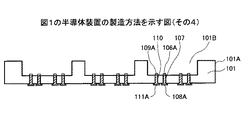
まず、図3Aに示す工程において、例えばSiよりなる基板101をエッチングしてパターニングし、発光素子を設置するための凹部101Bと、ビアプラグ107、110を形成するための、基板101を貫通するビアホール107A,110Aを形成する。
First, in the process shown in FIG. 3A, the
次に、図3Bに示す工程において、凹部101Bの内壁面やビアホール107A,110Aの内壁面を含む前記基板101の表面に、例えば熱CVD法などにより、酸化膜(シリコン酸化膜、または熱酸化膜と呼ぶ場合もある)101Aを形成する。
Next, in the step shown in FIG. 3B, an oxide film (silicon oxide film or thermal oxide film) is formed on the surface of the
次に、図3Cに示す工程において、例えばCuのメッキ法(例えばセミアディティブ法)により、ビアホール107A、110Aに、それぞれビアプラグ107、110を形成する。
Next, in the step shown in FIG. 3C, via
次に、図3Dに示す工程において、例えばメッキ法により、例えばNi/Auよりなる接続層106A,109A,108A,111Aを形成する。この場合、接続層106A,109Aは、それぞれビアプラグ107,110の凹部101Bの側に、接続層108A,111Aは、それぞれビアプラグ107,110の凹部101Bの反対側に形成される。
Next, in the step shown in FIG. 3D, connection layers 106A, 109A, 108A, 111A made of, for example, Ni / Au are formed by, for example, plating. In this case, the connection layers 106A and 109A are formed on the
次に、図3Eに示す工程において、接続層106A,109A上に、それぞれバンプ(Auスタッドバンプ)106,109を形成する。なお、本図以降では、接続層106A,109Aの図示を省略している。 Next, in the step shown in FIG. 3E, bumps (Au stud bumps) 106 and 109 are formed on the connection layers 106A and 109A, respectively. In the following drawings, the connection layers 106A and 109A are not shown.
次に、図3Fに示す工程において、凹部101Bの周囲の凸部101Cの表面の酸化膜101Aを、例えばマスクエッチにより剥離する。本工程によって酸化膜が剥離された部分には後の工程においてガラスよりなるカバーが接合される。
Next, in the step shown in FIG. 3F, the
次に、図3Gに示す工程において、前述した手順1〜5により光反射防止膜130が形成された発光素子102を、光反射防止膜130の形成面を上面として凹部101Bに設置する。この場合、例えば熱圧着、または超音波接合などを用いて、発光素子102とバンプ106を電気的に接合し、バンプ106を介して発光素子102とビアプラグ107が電気的に接続されるように構成する。
Next, in the step shown in FIG. 3G, the
次に、図3Hに示す工程において、例えばFe、Ni、Coなどの合金の表面にAgまたはAlの反射膜が形成されてなるリフレクタ105を、凹部101Bに設置する。この場合、例えば熱圧着、または超音波接合などを用いて、リフレクタ105とバンプ109を接合し、バンプ109を介してリフレクタ105とビアプラグ110が接続されるように構成する。
Next, in the step shown in FIG. 3H, a
次に、図3Iに示す工程において、例えばホウケイ酸ガラスよりなる、透過性を有する平板状のカバー103の上面に真空蒸着法などにより光透過率の良い誘電体膜を多層コーティングして光反射防止膜140を形成する。さらに、カバー103の下面に、蛍光体膜104をパターニングして形成する。本実施例による半導体装置の製造方法では、上記のように、平板状のカバー103の上下面の夫々に光反射防止膜140、蛍光体膜104を形成しているため、光反射防止膜140、蛍光体膜104の膜厚の均一性を良好に保つことができる。そのために半導体装置の発光の強度や発光色の均一性を高めることができる。
Next, in the step shown in FIG. 3I, light reflection prevention is performed by coating a dielectric film having a good light transmittance on the upper surface of a
また、この場合、カバー103と基板101とが接合される部分には、蛍光体膜104を形成せず、カバー103と基板101が直接接触するように蛍光体膜がパターニングされることが好ましい。
In this case, it is preferable that the phosphor film is patterned so that the
次に、図3Jに示す工程において、カバー103と基板101を、例えば陽極接合により接合し、発光素子102を基板101上で封止する構造が形成される。この場合、陽極接合は、カバー103と基板101との間に高電圧を印加し、カバー103と基板101を昇温して行う。
Next, in the step shown in FIG. 3J, a structure is formed in which the
上記の陽極接合が行われると、基板を構成するSiと、カバーを構成するガラス中の酸素が結合し、接合力が良好で安定した接合が行われる。また、樹脂材料を用いた接合と異なり、発光素子102が封止される空間を汚染するようなガス、不純物などが殆ど発生することがない。
When the above-described anodic bonding is performed, Si constituting the substrate and oxygen in the glass constituting the cover are bonded to each other, and the bonding force is good and stable bonding is performed. Unlike bonding using a resin material, almost no gas, impurities, or the like that contaminates the space in which the light-emitting
次に、図3Kに示す工程において、接続層108A,111Aにそれぞれ半田バンプ108,111を形成する。 Next, in the step shown in FIG. 3K, solder bumps 108 and 111 are formed on the connection layers 108A and 111A, respectively.
次に、図3Lに示す工程において、基板101とカバー103をダイシングにより切断し、個片化することで、先に説明した半導体装置100(図2を参照)が完成する。
Next, in the step shown in FIG. 3L, the
上記説明では、発光素子102上の光反射防止膜130は、個片化の前に形成した場合について説明したが、発光素子102を基板101に実装後に形成し、パターニングする方法を用いても良い。
In the above description, the case where the light
また、カバー103上の光反射防止膜140は、ウェーハレベルパッケージの場合、パッケージ個片化の前に形成してもよいし、個片化後に形成する方法を用いても良い。
Further, in the case of a wafer level package, the light
また、カバー103の上面だけでなく側壁にも光反射防止膜を形成するようにしても良い。その場合は、カバー103を切断する際にカバー103のみハーフダイシングした後、カバー103の側面に誘電体膜を多層コーティングして光反射防止膜を形成するようにしても良い。
Further, an antireflection film may be formed not only on the upper surface of the
また、本発明による半導体装置は、実施例1に記載した構造に限定されず、例えば以下に説明するように、様々に構成することが可能である。 Further, the semiconductor device according to the present invention is not limited to the structure described in the first embodiment, and can be variously configured as described below, for example.
図4は、本発明の実施例2による半導体装置200を模式的に示した断面図である。図2を参照するに、半導体装置200は、例えばSiよりなる基板201に、例えばLEDよりなる発光素子202が実装されてなる半導体装置である。発光素子202は、サファイア(Al2O3)を基材としてP層、N層、電極などが形成されており、その上面には、光の反射を防止する光反射防止膜230が形成されている。この光反射防止膜230は、例えば、多層反射防止膜(EBC:electron beam coating)、あるいはARコ−ティング(anti-reflective coating)と呼ばれる反射防止処理が施され、例えば真空蒸着等により形成された透明な薄膜である。
FIG. 4 is a cross-sectional view schematically showing a
また、発光素子202上には光透過性の、例えばガラスよりなる平板状のカバー203が設置され、当該カバー203の上面にも光の反射を防止する光反射防止膜240が形成されている。この光反射防止膜240は、前述した光反射防止膜230と同様に、多層反射防止膜(EBC:electron beam coating)などからなり、光の反射を防止してカバー103を透過する光量を相対的に増大させることができる。そのため、発光素子202からの光がカバー203を透過して屈折率の大きいガラス製のカバー203から屈折率の小さい空気へ進行する過程で全反射することが防止される。これにより、カバー203の上方に進行する光の光強度を向上させることができる。
Further, a light-transmitting
本実施例においては、半導体装置200から放射される光の強度を高めるために、発光素子202の上面に光反射防止膜230に形成し、且つカバー203の上面にも光反射防止膜240を形成した構成例を説明しているが、本発明では、光反射防止膜230,240の両方でも良いし、あるいは光反射防止膜230,240の何れか一方のみを形成した構成として良い。また、カバー203の上面だけでなく下面にも光反射防止膜を形成する構成とすることにより、例えば、後述する蛍光体膜204がガラスよりも屈折率の大きい物質からなる場合には、光の透過率を高めて光強度を向上させることができる。
In this embodiment, in order to increase the intensity of light emitted from the
尚、本実施例では、発光素子202が基板201に実装される構成について説明しているが、発光素子のみではなく、例えば、受光素子を実装した構成の半導体装置にも本発明を適用することができるのは、勿論である。その場合、光反射防止膜230,240は、外部から入射された光の反射を防止して受光される光強度を高めることができる。
In the present embodiment, the configuration in which the
さらに、当該カバー203の下面には蛍光体膜204が形成されている。この場合、本実施例による、基板201、発光素子202、カバー203、および蛍光体膜204は、実施例1の場合の基板101、発光素子102、カバー103、および蛍光体膜104に相当し、本実施例による半導体装置200は、実施例1の半導体装置100と同様の効果を有する。
Further, a
すなわち、半導体装置200では、蛍光体膜または蛍光体を含む樹脂などが直接発光素子(LED)上に塗布されることがないため、発光素子202の放熱が良好となり、発光素子の発熱による品質低下の影響が抑制されている。
That is, in the
また、蛍光体膜204が、発光素子202からの放熱や紫外線の照射などにより劣化する影響が抑制され、半導体装置を高品質とするとともに長寿命化をはかることが可能となっている。
In addition, the influence of deterioration of the
また、本実施例による半導体装置200では、略平板状の前記カバー203に、前記蛍光体膜が、例えば印刷法により形成されているため、蛍光体膜の膜厚の均一性が良好である特徴を有している。すなわち、本実施例による半導体装置200では、平板状の前記カバー203に蛍光体膜204を形成しているため、例えば印刷法などを用いて、蛍光体膜204を膜厚の均一性を良好に形成することができる。さらに、本実施例による半導体装置では、前記発光素子202の側面に蛍光体膜を形成する必要がなく、そのために発光の強度や発光色の均一性が良好である特徴を有する。
Further, in the
また、発光素子202は、例えばAuよりなるバンプ(Auスタッドバンプ)206上に設置され、当該発光素子202は、当該バンプ206を介して基板201の底面を貫通するように形成されるビアプラグ(貫通配線)207と電気的に接続されている。
The
ビアプラグ207の、発光素子202が接続される側の反対側には、例えばNi/Auメッキ層よりなる接続層208Aが形成され、さらに当該接続層208Aに半田バンプ208が形成されている。すなわち、ビアプラグ207が形成されることによって、発光素子202と、当該発光素子202が封止される空間の外側の接続対象とを、容易に接続することが可能になっている。また、バンプ207とビアプラグ207の間にも、例えばNi/Auメッキ層よりなる接続層が形成されていてもよいが、本図では図示を省略している。
A
また、基板201の表面は、酸化膜(シリコン酸化膜)201Aが形成され、例えば当該基板201と、ビアプラグ207との間や、バンプ206との間は絶縁されている。
Further, an oxide film (silicon oxide film) 201A is formed on the surface of the
本実施例による半導体装置200の場合、実施例1の半導体装置100と以下の点で相違しており、本実施例特有の効果を有している。
The
本実施例による半導体装置200は、発光素子202からの発光を反射するリフレクタ205(前記リフレクタ105に相当)を有するとともに、当該リフレクタ205が、基板201およびカバー203とともに、発光素子202を封止する封止空間201Bを画成している。
The
この場合、リフレクタ205の一端は、基板201上に形成された、例えばAuよりなる接合層210により当該基板101に接合される。また、リフレクタ205の他の一端は、例えばAuよりなる接合層209により、カバー203に接合されている。すなわち、リフレクタ203が、基板101、およびカバー204の双方と接合されることで、発光素子202が封止される封止空間201Bが形成されている。
In this case, one end of the
このため、封止空間201Bを、例えば減圧状態としたり、または不活性ガスで満たすことが可能となり、発光素子202の品質の維持と長寿命化を図ることが可能となっている。
Therefore, the sealed
また、基板201に、実施例1に記載したビアプラグ110に相当する放熱配線を形成し、リフレクタ205に接続することで、当該リフレクタ205の放熱性が良好となる構造(実施例1と同様の構造)としてもよい。
In addition, a heat dissipation wiring corresponding to the via
本実施例による半導体装置200では、基板201の構造(形状)が基板101に比べて単純であり、当該基板201の加工が容易となる特徴を有している。また、リフレクタが外気に曝される構造であるため、半導体装置100と比べるとさらに放熱性が良好であるメリットがある。
The
次に、上記の半導体装置200を製造する製造方法の一例について、図5A〜図5Mに基づき、手順を追って説明する。ただし以下の図中、先に説明した部分には同一の参照符号を付し、説明を省略する場合がある。
Next, an example of a manufacturing method for manufacturing the
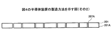
まず、図5Aに示す工程において、例えばSiよりなる基板201をエッチングしてパターニングし、ビアプラグ207を形成するための、基板201を貫通するビアホール207Aを形成する。
First, in the step shown in FIG. 5A, the
次に、図5Bに示す工程において、ビアホール207Aの内壁面を含む基板201の表面に、例えば熱CVD法などにより、酸化膜(シリコン酸化膜、または熱酸化膜とよぶ場合もある)201Aを形成する。
Next, in the step shown in FIG. 5B, an oxide film (sometimes called a silicon oxide film or a thermal oxide film) 201A is formed on the surface of the
次に、図5Cに示す工程において、例えばCuのメッキ法(例えばセミアディティブ法)により、ビアホール207Aにビアプラグ207を形成する。
Next, in the step shown in FIG. 5C, via
次に、図5Dに示す工程において、ビアプラグ207に対して、例えばメッキ法により、例えばNi/Auよりなる接続層206A,208Aを形成する。この場合、ビアプラグ207に対して、接続層206Aは後の工程で発光素子が実装される第1の側に、接続層208Aは当該第1の側の反対側の第2の側に形成される。また、基板201の第1の側には、後の工程においてリフレクタを接合するための、例えばAuよりなる接合層210をスパッタリング法またはメッキ法などにより、形成する。なお、本図以降では、接続層206A,209Aの図示を省略している。
Next, in the step shown in FIG. 5D, connection layers 206A and 208A made of, for example, Ni / Au are formed on the via
次に、図5Eに示す工程において、前記接続層206A上に、バンプ(Auスタッドバンプ)206を形成する。
Next, in the step shown in FIG. 5E, bumps (Au stud bumps) 206 are formed on the
次に、図5Fに示す工程において、例えばLEDよりなる発光素子202を、基板201上に設置する。この場合、例えば熱圧着、または超音波接合などを用いて、前述した手順1〜5により光反射防止膜230が形成された発光素子202とバンプ206を電気的に接合し、バンプ206を介して発光素子202とビアプラグ207が電気的に接続されるように構成する。
Next, in the step shown in FIG. 5F, a
次に、図5Gに示す工程において、基板201をダイシングにより切断し、発光素子202が実装された基板201を個片化する。
Next, in a step shown in FIG. 5G, the
次に、図5Hに示す工程において、例えばホウケイ酸ガラスよりなる、平板状のカバー203の上面に、例えば、真空蒸着法により光透過率の良い誘電体膜を多層コーティングして光反射防止膜240を形成する。さらに、カバー203の下面に、蛍光体膜204をパターニングして形成する。本実施例による半導体装置の製造方法では、上記のように、平板状のカバー203の上下面の夫々に光反射防止膜240、蛍光体膜204を形成しているため、光反射防止膜240、蛍光体膜204の膜厚の均一性を良好に保つことができる。そのために半導体装置200の発光の強度や発光色の均一性を高めることができる。
Next, in the step shown in FIG. 5H, a dielectric film having a good light transmittance is coated on the upper surface of the
次に、図5Iに示す工程において、カバー203に対して、後の工程においてリフレクタ209が接合されるための、例えばAuよりなる接合層209を、例えばスパッタリング法により、形成する。
Next, in the step shown in FIG. 5I, a
次に、図5Jに示す工程において、例えばFe、Ni、Coなどの合金の表面にAgまたはAlの反射膜が形成されてなるリフレクタ205の上端を、接合層209に接合する。この場合、例えば熱圧着、または超音波接合などを用いて、リフレクタ205と接合層209を接合する。
Next, in the step shown in FIG. 5J, the upper end of the
次に、図5Kに示す工程において、カバー203に接合されたリフレクタ205の下端と、発光素子202が実装された基板201とを接合する。この場合、例えば熱圧着、または超音波接合などを用いて、リフレクタ205と接合層210を接合する。このようにして、発光素子202が封止される封止空間201Bが形成され、基板201上で発光素子202が封止される。
Next, in the step shown in FIG. 5K, the lower end of the
次に、図5Lに示す工程において、接続層208Aに半田バンプ208を形成する。
Next, in the step shown in FIG. 5L, solder bumps 208 are formed on the
次に、図5Mに示す工程において、カバー203をダイシングにより切断し、個片化することで、先に説明した半導体装置200(図4参照)を形成することができる。
Next, in the step shown in FIG. 5M, the
本実施例より製造される半導体装置200は、基板201の構造(形状)が実施例1の基板101に比べて単純であるとともに、リフレクタが外気に曝される構造であるため、実施例1の半導体装置100と比べるとさらに放熱性が良好である特徴を有している。
In the
図6は実施例3の半導体装置を示す図である。図6に示されるように、半導体装置300は、基板301上に発光素子302が接着層320を介して固着される。発光素子302の上面には、光反射防止膜330が形成されている。
FIG. 6 is a diagram illustrating a semiconductor device according to the third embodiment. As shown in FIG. 6, in the
基板301は、上面から下面に貫通するビアプラグ307が形成されており、ビアプラグ307の下端が基板301の下面に形成された配線パターン308に電気的に接続されている。さらに、ビアプラグ307の上端は、発光素子302の電極(図示せず)にボンディングワイヤ322を介して接続される。
The
また、発光素子302が実装された基板301の上面には、例えばホウケイ酸ガラスよりなる、半球面形状のカバー303が接合層310を介して接合されている。このカバー303は、内側も半球面形状に形成されており、外周面には光反射防止膜340が形成され、内周面には蛍光体膜304が形成されている。
A
上記光反射防止膜330,340は、前述した実施例1,2と同様に、例えば、真空蒸着法などにより光透過率の良い誘電体膜を多層コーティングして形成された透明膜である。従って、この光反射防止膜330,340は、前述した実施例1,2と同様に、多層反射防止膜(EBC:electron beam coating)などからなり、光の反射を防止して発光素子302、カバー303を透過する光量を相対的に増大させることができる。そのため、発光素子302からの光がカバー303を透過して屈折率の大きいガラス製のカバー303から屈折率の小さい空気へ進行する過程で全反射することが防止される。これにより、カバー303から外部に進行する光の光強度を向上させることができる。
The light
本実施例においては、半導体装置300から放射される光の強度を高めるために、発光素子302の上面に光反射防止膜330に形成し、且つカバー303の上面にも光反射防止膜340を形成した構成例を説明しているが、本発明では、光反射防止膜330,340の両方でも良いし、あるいは光反射防止膜330,340の何れか一方のみを形成した構成として良い。また、半球面形状とされたカバー303の外周面だけでなく内周面にも光反射防止膜を形成する構成とすることにより、例えば、蛍光体膜304がガラスよりも屈折率の大きい物質からなる場合には、光の透過率を高めて光強度を向上させることができる。
In this embodiment, in order to increase the intensity of light emitted from the
尚、本実施例では、発光素子302が基板301に実装される構成について説明しているが、発光素子のみではなく、例えば、受光素子を実装した構成の半導体装置にも本発明を適用することができるのは、勿論である。その場合、光反射防止膜330,340は、外部から入射された光の反射を防止して受光される光強度を高めることができる。
In this embodiment, the configuration in which the
以上、本発明を好ましい実施例について説明したが、本発明は上記の特定の実施例に限定されるものではなく、特許請求の範囲に記載した要旨内において様々な変形・変更が可能である。 Although the present invention has been described with reference to the preferred embodiments, the present invention is not limited to the specific embodiments described above, and various modifications and changes can be made within the scope described in the claims.
尚、上記実施例では、LEDよりなる発光素子を例に挙げて説明したが、これに限らず、LED以外の発光素子が実装された半導体装置にも適用できるのは言うまでもない。 In the above-described embodiment, the light emitting element made of the LED has been described as an example. However, the present invention is not limited to this, and needless to say, the present invention can be applied to a semiconductor device on which a light emitting element other than the LED is mounted.
また、上記実施例では、真空蒸着法を用いた多層反射防止膜(EBC:electron beam coating)やARコ−ティング(anti-reflective coating)と呼ばれる反射防止処理により光反射防止膜が形成される場合について説明したが、これに以外の薄膜形成方法を用いて光反射防止膜を形成しても良いのは勿論である。 Moreover, in the said Example, when an antireflection film is formed by the antireflection process called multilayer antireflection film (EBC: electron beam coating) and AR coating (anti-reflective coating) using the vacuum evaporation method However, it is a matter of course that the light reflection preventing film may be formed by using a thin film forming method other than this.
また、上記実施例では、発光素子を封止するカバーが平板状のものと半球形状のものを一例として挙げたが、カバーの形状は、これに限らず、例えば、凸レンズ状のものやあるいは有底円筒形状のもの等でも良いのは勿論である。 In the above embodiment, the cover for sealing the light emitting element has been exemplified as a flat plate and a hemispherical cover. However, the shape of the cover is not limited to this. Of course, a bottom cylindrical shape or the like may be used.
100,200,300 半導体装置
101,201,301 基板
102,202,302 発光素子
103,203,303 カバー
104,204,304 蛍光体膜
105,205 リフレクタ
130,140,230,240,330,340 光反射防止膜
100, 200, 300
Claims (7)
前記光機能素子上には光透過性を有するカバーが設置され、
前記カバーの上面及び前記光機能素子の上面に光の反射を防止する光反射防止膜が形成され、
前記カバーの下面に蛍光体膜が形成され、
前記基板を貫通する貫通配線及び放熱配線が形成され、
前記光機能素子の側面を囲むように、金属部材の表面に反射膜が形成されてなる、光を反射するリフレクタが配置され、
前記リフレクタと前記放熱配線とが接続され、
前記光機能素子は、バンプを介して前記貫通配線と電気的に接続され、
前記放熱配線は、前記貫通配線の外側に設けられていることを特徴とする半導体装置。 A semiconductor device in which an optical functional element is mounted on a substrate,
A cover having optical transparency is installed on the optical functional element,
An antireflection film for preventing light reflection is formed on the upper surface of the cover and the upper surface of the optical functional element,
A phosphor film is formed on the lower surface of the cover,
A through wiring and a heat radiation wiring penetrating the substrate are formed,
A reflector that reflects light is formed by forming a reflective film on the surface of the metal member so as to surround the side surface of the optical functional element,
The reflector and the heat dissipation wiring are connected ,
The optical functional element is electrically connected to the through wiring via a bump,
The semiconductor device , wherein the heat radiation wiring is provided outside the through wiring .
前記光機能素子の上面に光反射防止膜を形成する工程と、
前記基板上に設置された前記光機能素子を、光透過性を有するカバーを用いて封止する工程と、
前記カバーの上面に光反射防止膜を形成する工程と、
前記カバーの下面に蛍光体膜を形成する工程と、
前記基板を貫通しバンプを介して前記光機能素子と電気的に接続される貫通配線を形成し、前記貫通配線の外側に前記基板を貫通する放熱配線を形成する工程と、
前記光機能素子の側面を囲むように、金属部材の表面に反射膜が形成されてなる、光を反射するリフレクタを配置する工程と、
前記リフレクタと前記放熱配線とを接続する工程と、
を有することを特徴とする半導体装置の製造方法。 Mounting the optical functional element on the substrate;
Forming an antireflection film on the upper surface of the optical functional element;
Sealing the optical functional element placed on the substrate with a cover having light transparency;
Forming an antireflection film on the upper surface of the cover;
Forming a phosphor film on the lower surface of the cover;
Forming a through-wiring that penetrates the substrate and is electrically connected to the optical functional element via a bump, and forming a heat dissipation wiring that penetrates the substrate outside the through-wiring ;
A step of disposing a reflector that reflects light, in which a reflective film is formed on the surface of the metal member so as to surround a side surface of the optical functional element;
Connecting the reflector and the heat dissipation wiring;
A method for manufacturing a semiconductor device, comprising:
前記凹部の開口は、前記カバーを用いて封止されていることを特徴とする請求項4に記載の半導体装置の製造方法。 The substrate is formed with a recess for mounting the optical functional element,
The method of manufacturing a semiconductor device according to claim 4, wherein the opening of the recess is sealed with the cover.
前記リフレクタの下端を前記光機能素子が載置された領域の周囲に接合して前記光機能素子が実装された空間を封止する工程と、
を有することを特徴とする請求項4に記載の半導体装置の製造方法。 Joining the upper end of the reflector to the cover;
Bonding the lower end of the reflector to the periphery of the region where the optical functional element is placed, and sealing the space where the optical functional element is mounted;
The method of manufacturing a semiconductor device according to claim 4, wherein:
Priority Applications (4)
| Application Number | Priority Date | Filing Date | Title |
|---|---|---|---|
| JP2006025649A JP4996101B2 (en) | 2006-02-02 | 2006-02-02 | Semiconductor device and manufacturing method of semiconductor device |
| US11/700,761 US7825423B2 (en) | 2006-02-02 | 2007-02-01 | Semiconductor device and method of manufacturing semiconductor device |
| EP07002224A EP1816687A2 (en) | 2006-02-02 | 2007-02-01 | Semiconductor device and method of manufacturing semiconductor device |
| TW096103824A TW200805707A (en) | 2006-02-02 | 2007-02-02 | Semiconductor device and method of manufacturing semiconductor device |
Applications Claiming Priority (1)
| Application Number | Priority Date | Filing Date | Title |
|---|---|---|---|
| JP2006025649A JP4996101B2 (en) | 2006-02-02 | 2006-02-02 | Semiconductor device and manufacturing method of semiconductor device |
Publications (3)
| Publication Number | Publication Date |
|---|---|
| JP2007208041A JP2007208041A (en) | 2007-08-16 |
| JP2007208041A5 JP2007208041A5 (en) | 2008-12-25 |
| JP4996101B2 true JP4996101B2 (en) | 2012-08-08 |
Family
ID=38038555
Family Applications (1)
| Application Number | Title | Priority Date | Filing Date |
|---|---|---|---|
| JP2006025649A Expired - Fee Related JP4996101B2 (en) | 2006-02-02 | 2006-02-02 | Semiconductor device and manufacturing method of semiconductor device |
Country Status (4)
| Country | Link |
|---|---|
| US (1) | US7825423B2 (en) |
| EP (1) | EP1816687A2 (en) |
| JP (1) | JP4996101B2 (en) |
| TW (1) | TW200805707A (en) |
Families Citing this family (38)
| Publication number | Priority date | Publication date | Assignee | Title |
|---|---|---|---|---|
| KR100883075B1 (en) * | 2007-03-02 | 2009-02-10 | 엘지전자 주식회사 | Light Emitting Device |
| DE102008005344A1 (en) | 2007-09-21 | 2009-04-02 | Osram Opto Semiconductors Gmbh | Radiation-emitting component |
| EP2048717A1 (en) * | 2007-10-10 | 2009-04-15 | Unity Opto Technology Co., Ltd. | Structure of light-emitting diode |
| JP5089336B2 (en) * | 2007-10-29 | 2012-12-05 | 新光電気工業株式会社 | Silicon substrate for package |
| JP4912275B2 (en) | 2007-11-06 | 2012-04-11 | 新光電気工業株式会社 | Semiconductor package |
| JP2010074117A (en) * | 2007-12-07 | 2010-04-02 | Panasonic Electric Works Co Ltd | Light emitting device |
| KR100998009B1 (en) * | 2008-03-12 | 2010-12-03 | 삼성엘이디 주식회사 | Light emitting diode package and method of manufacturing the same |
| US8890186B2 (en) * | 2008-03-28 | 2014-11-18 | Panasonic Corporation | Molded resin product, semiconductor light-emitting source, lighting device, and method for manufacturing molded resin product |
| DE102008025491A1 (en) * | 2008-05-28 | 2009-12-03 | Osram Opto Semiconductors Gmbh | Optoelectronic semiconductor component and printed circuit board |
| US8058669B2 (en) * | 2008-08-28 | 2011-11-15 | Taiwan Semiconductor Manufacturing Company, Ltd. | Light-emitting diode integration scheme |
| JP2010135488A (en) * | 2008-12-03 | 2010-06-17 | Toshiba Corp | Light-emitting device, and method of manufacturing the same |
| DE102009005547A1 (en) * | 2009-01-20 | 2010-07-29 | R. Stahl Schaltgeräte GmbH | Encapsulated light-emitting diode arrangement |
| KR101064026B1 (en) * | 2009-02-17 | 2011-09-08 | 엘지이노텍 주식회사 | Light emitting device package and manufacturing method thereof |
| JP5327042B2 (en) * | 2009-03-26 | 2013-10-30 | 豊田合成株式会社 | LED lamp manufacturing method |
| US20100301728A1 (en) * | 2009-06-02 | 2010-12-02 | Bridgelux, Inc. | Light source having a refractive element |
| WO2012011460A1 (en) * | 2010-07-22 | 2012-01-26 | 京セラ株式会社 | Light-emitting device |
| KR101714042B1 (en) * | 2010-08-05 | 2017-03-08 | 엘지이노텍 주식회사 | Light emitting device package |
| WO2012124473A1 (en) * | 2011-03-15 | 2012-09-20 | 京セラ株式会社 | Light emitting device |
| JP5769482B2 (en) * | 2011-04-18 | 2015-08-26 | セイコーインスツル株式会社 | Manufacturing method of glass sealed package and optical device |
| JP2013004901A (en) * | 2011-06-21 | 2013-01-07 | Nippon Kasei Chem Co Ltd | Led device |
| TW201310126A (en) * | 2011-08-18 | 2013-03-01 | Hon Hai Prec Ind Co Ltd | Light emitting device |
| CN103050583A (en) * | 2011-10-14 | 2013-04-17 | 展晶科技(深圳)有限公司 | Method for encapsulating light-emitting diode |
| KR101887942B1 (en) * | 2012-05-07 | 2018-08-14 | 삼성전자주식회사 | Light emitting device |
| JP6139071B2 (en) | 2012-07-30 | 2017-05-31 | 日亜化学工業株式会社 | Light emitting device and manufacturing method thereof |
| DE102013104240B4 (en) | 2013-04-26 | 2015-10-22 | R. Stahl Schaltgeräte GmbH | Explosion-proof arrangement of electrical and / or electronic components |
| JP6490932B2 (en) * | 2013-09-16 | 2019-03-27 | エルジー イノテック カンパニー リミテッド | Light emitting device package |
| DE102013111374A1 (en) * | 2013-10-15 | 2015-04-16 | R. Stahl Schaltgeräte GmbH | Explosion-proof arrangement for electrical and / or electronic components |
| CN104124324B (en) * | 2014-08-06 | 2017-03-01 | 华中科技大学 | A kind of LED packaged glass and its preparation method and application |
| US10681777B2 (en) * | 2016-04-01 | 2020-06-09 | Infineon Technologies Ag | Light emitter devices, optical filter structures and methods for forming light emitter devices and optical filter structures |
| US10347814B2 (en) | 2016-04-01 | 2019-07-09 | Infineon Technologies Ag | MEMS heater or emitter structure for fast heating and cooling cycles |
| US10559723B2 (en) * | 2017-08-25 | 2020-02-11 | Rohm Co., Ltd. | Optical device |
| US11758948B2 (en) | 2018-01-29 | 2023-09-19 | Altria Client Services Llc | Lighting unit for aerosol-generating systems |
| JP7376484B2 (en) * | 2018-01-29 | 2023-11-08 | フィリップ・モーリス・プロダクツ・ソシエテ・アノニム | Lighting unit for aerosol generation system |
| US11178392B2 (en) * | 2018-09-12 | 2021-11-16 | Apple Inc. | Integrated optical emitters and applications thereof |
| WO2020163139A2 (en) | 2019-02-04 | 2020-08-13 | Apple Inc. | Vertical emitters with integral microlenses |
| JP7239840B2 (en) * | 2020-08-31 | 2023-03-15 | 日亜化学工業株式会社 | Method for manufacturing light emitting device |
| WO2023042461A1 (en) * | 2021-09-14 | 2023-03-23 | ソニーグループ株式会社 | Semiconductor light-emitting device |
| CN114864796A (en) * | 2022-07-05 | 2022-08-05 | 至芯半导体(杭州)有限公司 | Ultraviolet device packaging structure and manufacturing method |
Family Cites Families (18)
| Publication number | Priority date | Publication date | Assignee | Title |
|---|---|---|---|---|
| JPS4846288A (en) * | 1971-10-13 | 1973-07-02 | ||
| JPH0328467Y2 (en) * | 1985-12-28 | 1991-06-19 | ||
| JPH06350132A (en) * | 1993-06-08 | 1994-12-22 | Victor Co Of Japan Ltd | Semiconductor luminous element array |
| US6784463B2 (en) * | 1997-06-03 | 2004-08-31 | Lumileds Lighting U.S., Llc | III-Phospide and III-Arsenide flip chip light-emitting devices |
| JP2003110146A (en) * | 2001-07-26 | 2003-04-11 | Matsushita Electric Works Ltd | Light-emitting device |
| JP3912607B2 (en) * | 2002-06-19 | 2007-05-09 | サンケン電気株式会社 | Manufacturing method of semiconductor light emitting device |
| US7224000B2 (en) * | 2002-08-30 | 2007-05-29 | Lumination, Llc | Light emitting diode component |
| JP4280050B2 (en) * | 2002-10-07 | 2009-06-17 | シチズン電子株式会社 | White light emitting device |
| EP1577956A1 (en) * | 2002-12-25 | 2005-09-21 | Japan Science and Technology Agency | Light emitting element device, light receiving element device, optical apparatus, fluoride crystal, process for producing fluoride crystal and crucible |
| KR20040092512A (en) * | 2003-04-24 | 2004-11-04 | (주)그래픽테크노재팬 | A semiconductor light emitting device with reflectors having a cooling function |
| EP1484802B1 (en) * | 2003-06-06 | 2018-06-13 | Stanley Electric Co., Ltd. | Optical semiconductor device |
| JP4138586B2 (en) * | 2003-06-13 | 2008-08-27 | スタンレー電気株式会社 | LED lamp for light source and vehicle headlamp using the same |
| US7560820B2 (en) * | 2004-04-15 | 2009-07-14 | Saes Getters S.P.A. | Integrated getter for vacuum or inert gas packaged LEDs |
| CN101032034A (en) * | 2004-06-30 | 2007-09-05 | 克里公司 | Chip-scale methods for packaging light emitting devices and chip-scale packaged light emitting devices |
| DE102005042778A1 (en) * | 2004-09-09 | 2006-04-13 | Toyoda Gosei Co., Ltd., Nishikasugai | Optical solid state device |
| US7365371B2 (en) * | 2005-08-04 | 2008-04-29 | Cree, Inc. | Packages for semiconductor light emitting devices utilizing dispensed encapsulants |
| US7798678B2 (en) * | 2005-12-30 | 2010-09-21 | 3M Innovative Properties Company | LED with compound encapsulant lens |
| US7521728B2 (en) * | 2006-01-20 | 2009-04-21 | Cree, Inc. | Packages for semiconductor light emitting devices utilizing dispensed reflectors and methods of forming the same |
-
2006
- 2006-02-02 JP JP2006025649A patent/JP4996101B2/en not_active Expired - Fee Related
-
2007
- 2007-02-01 US US11/700,761 patent/US7825423B2/en not_active Expired - Fee Related
- 2007-02-01 EP EP07002224A patent/EP1816687A2/en not_active Withdrawn
- 2007-02-02 TW TW096103824A patent/TW200805707A/en unknown
Also Published As
| Publication number | Publication date |
|---|---|
| JP2007208041A (en) | 2007-08-16 |
| EP1816687A2 (en) | 2007-08-08 |
| TW200805707A (en) | 2008-01-16 |
| US7825423B2 (en) | 2010-11-02 |
| US20070194712A1 (en) | 2007-08-23 |
Similar Documents
| Publication | Publication Date | Title |
|---|---|---|
| JP4996101B2 (en) | Semiconductor device and manufacturing method of semiconductor device | |
| JP5209177B2 (en) | Semiconductor device and manufacturing method of semiconductor device | |
| EP3364469B1 (en) | Light emitting diode having side reflection layer | |
| EP3767688B1 (en) | Light emitting diode | |
| US8399894B2 (en) | Semiconductor light emitting device | |
| TWI420688B (en) | Method of removing the growth substrate of a semiconductor light-emitting device | |
| JP6106120B2 (en) | Semiconductor light emitting device | |
| CN111129255B (en) | Light emitting diode | |
| JP6060994B2 (en) | Optical semiconductor device | |
| JP2005268323A (en) | Semiconductor light emitting device | |
| JP2006253298A (en) | Semiconductor light emitting element and device therefor | |
| JP2009267418A (en) | Light-emitting device, package and system including the same, and method of manufacturing the same | |
| KR20090002835A (en) | Nitride light emitting device and method of making the same | |
| TW201434182A (en) | Semiconductor light emitting device and method for manufacturing the same | |
| KR20160017849A (en) | High power light emitting device and method of making the same | |
| JP2012023184A (en) | Light-emitting device | |
| KR20150142110A (en) | Manufacturing method of light emitting device package | |
| JP5451534B2 (en) | Semiconductor light emitting device and method for manufacturing semiconductor light emitting device | |
| US11843078B2 (en) | Light emitting device with good visibility | |
| JP5034342B2 (en) | Light emitting device | |
| JP2008166661A (en) | Semiconductor light-emitting apparatus | |
| JP2013197310A (en) | Light-emitting device | |
| JP5249856B2 (en) | Light emitting device | |
| CN104966777A (en) | Semiconductor light-emitting device and method of manufacturing the same | |
| KR101021416B1 (en) | Light emitting diode having wavelength conversion piles and method for fabricating the same |
Legal Events
| Date | Code | Title | Description |
|---|---|---|---|
| A521 | Request for written amendment filed |
Free format text: JAPANESE INTERMEDIATE CODE: A523 Effective date: 20081107 |
|
| A621 | Written request for application examination |
Free format text: JAPANESE INTERMEDIATE CODE: A621 Effective date: 20081107 |
|
| A977 | Report on retrieval |
Free format text: JAPANESE INTERMEDIATE CODE: A971007 Effective date: 20110419 |
|
| A131 | Notification of reasons for refusal |
Free format text: JAPANESE INTERMEDIATE CODE: A131 Effective date: 20110510 |
|
| A521 | Request for written amendment filed |
Free format text: JAPANESE INTERMEDIATE CODE: A523 Effective date: 20110623 |
|
| A131 | Notification of reasons for refusal |
Free format text: JAPANESE INTERMEDIATE CODE: A131 Effective date: 20110906 |
|
| A521 | Request for written amendment filed |
Free format text: JAPANESE INTERMEDIATE CODE: A523 Effective date: 20111104 |
|
| TRDD | Decision of grant or rejection written | ||
| A01 | Written decision to grant a patent or to grant a registration (utility model) |
Free format text: JAPANESE INTERMEDIATE CODE: A01 Effective date: 20120508 |
|
| A01 | Written decision to grant a patent or to grant a registration (utility model) |
Free format text: JAPANESE INTERMEDIATE CODE: A01 |
|
| A61 | First payment of annual fees (during grant procedure) |
Free format text: JAPANESE INTERMEDIATE CODE: A61 Effective date: 20120511 |
|
| FPAY | Renewal fee payment (event date is renewal date of database) |
Free format text: PAYMENT UNTIL: 20150518 Year of fee payment: 3 |
|
| R150 | Certificate of patent or registration of utility model |
Ref document number: 4996101 Country of ref document: JP Free format text: JAPANESE INTERMEDIATE CODE: R150 Free format text: JAPANESE INTERMEDIATE CODE: R150 |
|
| LAPS | Cancellation because of no payment of annual fees |