JP2020004923A - Image processing apparatus, mounting apparatus, image processing method, and program - Google Patents
Image processing apparatus, mounting apparatus, image processing method, and program Download PDFInfo
- Publication number
- JP2020004923A JP2020004923A JP2018125868A JP2018125868A JP2020004923A JP 2020004923 A JP2020004923 A JP 2020004923A JP 2018125868 A JP2018125868 A JP 2018125868A JP 2018125868 A JP2018125868 A JP 2018125868A JP 2020004923 A JP2020004923 A JP 2020004923A
- Authority
- JP
- Japan
- Prior art keywords
- image
- board
- component
- unit
- substrate
- Prior art date
- Legal status (The legal status is an assumption and is not a legal conclusion. Google has not performed a legal analysis and makes no representation as to the accuracy of the status listed.)
- Granted
Links
Images


Classifications
-
- H—ELECTRICITY
- H05—ELECTRIC TECHNIQUES NOT OTHERWISE PROVIDED FOR
- H05K—PRINTED CIRCUITS; CASINGS OR CONSTRUCTIONAL DETAILS OF ELECTRIC APPARATUS; MANUFACTURE OF ASSEMBLAGES OF ELECTRICAL COMPONENTS
- H05K13/00—Apparatus or processes specially adapted for manufacturing or adjusting assemblages of electric components
- H05K13/08—Monitoring manufacture of assemblages
- H05K13/081—Integration of optical monitoring devices in assembly lines; Processes using optical monitoring devices specially adapted for controlling devices or machines in assembly lines
-
- Y—GENERAL TAGGING OF NEW TECHNOLOGICAL DEVELOPMENTS; GENERAL TAGGING OF CROSS-SECTIONAL TECHNOLOGIES SPANNING OVER SEVERAL SECTIONS OF THE IPC; TECHNICAL SUBJECTS COVERED BY FORMER USPC CROSS-REFERENCE ART COLLECTIONS [XRACs] AND DIGESTS
- Y02—TECHNOLOGIES OR APPLICATIONS FOR MITIGATION OR ADAPTATION AGAINST CLIMATE CHANGE
- Y02P—CLIMATE CHANGE MITIGATION TECHNOLOGIES IN THE PRODUCTION OR PROCESSING OF GOODS
- Y02P90/00—Enabling technologies with a potential contribution to greenhouse gas [GHG] emissions mitigation
- Y02P90/02—Total factory control, e.g. smart factories, flexible manufacturing systems [FMS] or integrated manufacturing systems [IMS]
Abstract
Description
本発明は、画像処理装置、実装装置、画像処理方法、プログラムに関する。 The present invention relates to an image processing device, a mounting device, an image processing method, and a program.
部品の表面実装では、生産プログラムの搭載座標に基づいて基板上の所定の搭載位置に部品が搭載されている(例えば、特許文献1参照)。CADシステムを採用したユーザでは、基板設計用のCADデータに基づいて生産プログラムに対して部品の搭載位置が数値入力される。一方で、CADシステムを採用していない少量多品種生産のユーザでは、基板をカメラで撮像すると共に、ディスプレイに表示した基板画像に対して部品画像をジョグ操作で動かすことで位置合わせして、生産プログラムに部品の搭載位置をティーチングしている。 In surface mounting of components, components are mounted at predetermined mounting positions on a substrate based on mounting coordinates of a production program (for example, see Patent Document 1). A user who adopts a CAD system inputs numerical values of component mounting positions into a production program based on CAD data for board design. On the other hand, users of small-quantity multi-product production that do not employ the CAD system take images of the board with a camera and align the parts image by jog operation with respect to the board image displayed on the display. Teaching the mounting position of parts to the program.
しかしながら、上記したように、CADシステムを持たないユーザでは、実際の基板に対して部品をジョグ操作によって1つずつ指定しなければならない。CADデータが無い状態でティーチングするのはユーザの負担が大きく時間もかかり、ティーチング後に搭載位置にズレが生じると、位置ズレを直すのにも時間がかかっていた。このように、実際の基板を用いた現物合わせでは、生産プログラムに対する搭載位置のティーチング作業をサポートする技術が求められていた。 However, as described above, a user who does not have a CAD system must specify components on an actual board one by one by a jog operation. Teaching without CAD data requires a large burden on the user and takes time, and if the mounting position shifts after teaching, it takes time to correct the position shift. As described above, in actual physical alignment using an actual substrate, a technology for supporting a teaching operation of a mounting position with respect to a production program has been required.
本発明はかかる点に鑑みてなされたものであり、ディスプレイで部品の搭載位置を容易に指定することができる画像処理装置、実装装置、画像処理方法、プログラムを提供することを目的の1つとする。 SUMMARY An advantage of some aspects of the invention is to provide an image processing apparatus, a mounting apparatus, an image processing method, and a program that can easily specify a mounting position of a component on a display. .
本発明の一態様の画像処理装置は、表面に回路パターンを形成した基板が撮像されて、当該基板に対する部品の搭載位置をディスプレイに指定可能に表示させる画像処理装置であって、基板表面を撮像した基板画像を取得する第1の取得部と、部品底面を撮像した部品画像を取得する第2の取得部と、部品画像の特徴点を基板画像の回路パターンに照合する照合部と、基板画像上の照合箇所を搭載位置として強調表示する表示制御部とを備えたことを特徴とする。 An image processing apparatus according to one embodiment of the present invention is an image processing apparatus in which a substrate on which a circuit pattern is formed is imaged and a mounting position of a component with respect to the substrate is displayed on a display so as to be specified. A first obtaining unit for obtaining a printed board image, a second obtaining unit for obtaining a component image obtained by imaging a bottom surface of the component, a matching unit for checking feature points of the component image with a circuit pattern of the board image, and a board image. A display control unit for highlighting the upper collation part as a mounting position.
本発明の一態様の画像処理方法は、表面に回路パターンを形成した基板が撮像されて、当該基板に対する部品の搭載位置をディスプレイに指定可能に表示させる画像処理方法であって、基板表面を撮像した基板画像を取得するステップと、部品底面を撮像した部品画像を取得するステップと、部品画像の特徴点を基板画像の回路パターンに照合するステップと、基板画像上の照合箇所を搭載位置として強調表示するステップとを有することを特徴とする。 An image processing method according to one embodiment of the present invention is an image processing method in which a substrate on which a circuit pattern is formed is imaged and a mounting position of a component on the substrate is displayed on a display so as to be specified. Obtaining a component image obtained by capturing the bottom surface of the component, collating feature points of the component image with a circuit pattern of the substrate image, and emphasizing a collation location on the substrate image as a mounting position. And displaying.
これらの構成によれば、部品底面の特徴点と基板表面の回路パターンの照合結果に応じて、ディスプレイに映された基板画像上で部品の搭載位置が強調表示される。基板画像上で強調表示された搭載位置を指定することで、CADデータを使用することなく、生産プログラムに搭載位置のティーチングを行うことができる。よって、部品の搭載位置を容易に指定することができ、ユーザの作業負担を軽減する共に作業時間を短縮することができる。 According to these configurations, the mounting position of the component is highlighted on the board image displayed on the display in accordance with the result of matching the feature point on the bottom surface of the component with the circuit pattern on the board surface. By specifying the mounting position highlighted on the board image, the mounting position can be taught in the production program without using CAD data. Therefore, the mounting position of the component can be easily specified, and the work load on the user can be reduced, and the work time can be shortened.
本発明の一態様の画像処理装置において、前記表示制御部は、前記照合部の照合結果で相関が高い方から上位数箇所を搭載位置の候補として強調表示する。この構成によれば、基板画像上に複数の搭載位置の候補が表示され、複数の搭載位置の候補から所望の搭載位置を選択することができる。 In the image processing device according to one aspect of the present invention, the display control unit highlights, as candidates for the mounting position, several places in the order of higher correlation in the matching result of the matching unit. According to this configuration, a plurality of mounting position candidates are displayed on the board image, and a desired mounting position can be selected from the plurality of mounting position candidates.
本発明の一態様の画像処理装置において、前記表示制御部は、部品の底面認識用のテンプレート画像を表裏反転させて、当該テンプレート画像を搭載位置に重ねることで照合箇所を強調表示する。この構成によれば、既存のテンプレート画像を流用して照合箇所を強調表示することができる。 In the image processing device according to an aspect of the present invention, the display control unit may invert the template image for recognizing the bottom surface of the component, and highlight the collation location by superimposing the template image on the mounting position. According to this configuration, the collation location can be highlighted using the existing template image.
本発明の一態様の画像処理装置において、基板が同一回路パターンの複数の単位基板から成る多面取り基板であり、一の単位基板の回路パターンに対する他の単位基板の回路パターンのオフセット量を検出する検出部と、一の単位基板の搭載位置と回路パターンのオフセット量から他の単位基板の搭載位置を求める算出部とを備える。この構成によれば、一の単位基板の搭載位置を指定することで、他の単位基板の搭載位置を自動的に指定することができる。 In the image processing device of one embodiment of the present invention, the substrate is a multi-panel substrate including a plurality of unit substrates having the same circuit pattern, and an offset amount of a circuit pattern of another unit substrate with respect to a circuit pattern of one unit substrate is detected. A detection unit; and a calculation unit that determines a mounting position of another unit substrate from a mounting position of one unit substrate and an offset amount of a circuit pattern. According to this configuration, by specifying the mounting position of one unit substrate, it is possible to automatically specify the mounting position of another unit substrate.
本発明の一態様の画像処理装置において、前記検出部は、多面取り基板の2つの基板画像を縦横方向にシフトしながら回路パターンの相関を求め、相関がある箇所に基づいて回路パターンのオフセット量を検出する。この構成によれば、複数の単位基板の回路パターンが同じ向きの場合に、一の単位基板に対する他の単位基板の回路パターンのオフセット量を検出することができる。 In the image processing apparatus according to one aspect of the present invention, the detection unit obtains a correlation between the circuit patterns while shifting the two board images of the multi-panel board in the vertical and horizontal directions, and determines an offset amount of the circuit pattern based on the location having the correlation. Is detected. According to this configuration, when the circuit patterns of the plurality of unit substrates are in the same direction, the offset amount of the circuit pattern of another unit substrate with respect to one unit substrate can be detected.
本発明の一態様の画像処理装置において、前記検出部は、多面取り基板の2つの基板画像を回転方向にシフトしながら回路パターンの相関を求め、相関がある箇所に基づいて回路パターンのオフセット角を検出する。この構成によれば、複数の単位基板の回路パターンが異なる向きの場合に、一の単位基板に対する他の単位基板の回路パターンのオフセット角を検出することができる。 In the image processing apparatus according to one aspect of the present invention, the detection unit obtains a correlation of the circuit pattern while shifting the two board images of the multi-panel board in the rotation direction, and determines an offset angle of the circuit pattern based on the location where the correlation exists. Is detected. According to this configuration, when the circuit patterns of the plurality of unit substrates are in different directions, the offset angle of the circuit pattern of another unit substrate with respect to one unit substrate can be detected.
本発明の一態様の画像処理装置において、計測部によって多面取り基板を横切りながら計測された高さデータに基づいて基板画像を切り出す切り出し部を備え、前記検出部は、切り出し後の2つの基板画像をシフトしながら回路パターンの相関を求める。この構成によれば、基板が存在していない余白部分を基板画像から取り除くことで、基板画像の画像サイズを小さくして回路パターンのオフセット量又はオフセット角の検出処理時の処理量を低減することができる。 The image processing apparatus according to one aspect of the present invention includes a cutout unit that cuts out a board image based on height data measured while traversing the multi-surface board by the measurement unit, wherein the detection unit includes two cutout board images. While calculating the correlation of the circuit pattern. According to this configuration, by removing the blank portion where the board is not present from the board image, the image size of the board image is reduced, and the processing amount at the time of detecting the offset amount or the offset angle of the circuit pattern is reduced. Can be.
本発明の一態様の実装装置は、上記の画像処理装置と、前記画像処理装置で指定された搭載位置に部品を搭載する搭載ヘッドとを備えたことを特徴とする。この構成によれば、画像処理装置で指定した搭載位置に搭載ヘッドで部品を搭載することができる。また、初回の搭載位置を生産プログラムに反映することで、2枚目以降の基板に対する搭載処理を高速化することができる。 A mounting apparatus according to one embodiment of the present invention includes the image processing apparatus described above, and a mounting head that mounts a component at a mounting position designated by the image processing apparatus. According to this configuration, the component can be mounted by the mounting head at the mounting position designated by the image processing apparatus. In addition, by reflecting the initial mounting position in the production program, the mounting process for the second and subsequent substrates can be speeded up.
本発明の一態様のプログラムは、表面に回路パターンを形成した基板が撮像されて、当該基板に対する部品の搭載位置をディスプレイに指定可能に表示させる画像処理装置のプログラムであって、基板表面を撮像した基板画像を取得するステップと、部品底面を撮像した部品画像を取得するステップと、部品画像の特徴点を基板画像の回路パターンに照合するステップと、基板画像上の照合箇所を搭載位置として強調表示するステップとを前記画像処理装置に実行させることを特徴とする。この構成によれば、画像処理装置にプログラムをインストールすることで、ディスプレイで部品の搭載位置を容易に指定可能な機能を画像処理装置に追加することができる。 A program according to one embodiment of the present invention is a program for an image processing apparatus which captures an image of a substrate on which a circuit pattern is formed on a surface and displays a mounting position of a component on the substrate so that the mounting position can be specified on a display. Obtaining a component image obtained by capturing the bottom surface of the component, collating feature points of the component image with a circuit pattern of the substrate image, and emphasizing a collation location on the substrate image as a mounting position. The displaying step is performed by the image processing apparatus. According to this configuration, by installing the program in the image processing apparatus, it is possible to add to the image processing apparatus a function capable of easily designating the mounting position of the component on the display.
本発明によれば、部品底面の特徴点と基板表面の回路パターンの照合結果に応じて、基板画像上で搭載位置を強調表示することで、部品の搭載位置を容易に指定することができる。 According to the present invention, the mounting position of the component can be easily designated by highlighting the mounting position on the board image in accordance with the result of matching between the characteristic point on the bottom surface of the component and the circuit pattern on the board surface.
以下、添付図面を参照して、本実施の形態の画像処理装置を備えた実装装置について説明する。図1は、本実施の形態の実装装置の上面模式図である。なお、本実施の形態の実装装置は一例に過ぎず、適宜変更が可能である。 Hereinafter, a mounting apparatus including the image processing apparatus according to the present embodiment will be described with reference to the accompanying drawings. FIG. 1 is a schematic top view of the mounting apparatus of the present embodiment. The mounting device according to the present embodiment is merely an example, and can be appropriately changed.
図1に示すように、実装装置1は、フィーダ13によって供給された部品P(図2参照)を、搭載ヘッド30によって基板60の所定位置に搭載するように構成されている。実装装置1の基台10の略中央には、X軸方向に基板60を搬送する基板搬送部11が配設されている。基板搬送部11は、X軸方向の一端側から部品搭載前の基板60を搭載ヘッド30の下方に搬入して位置決めし、部品搭載後の基板60をX軸方向の他端側から搬出している。また、基板搬送部11を挟んだ両側には、複数のフィーダ13がX軸方向に横並びに配置されたフィーダバンク12が分離可能に連結されている。
As shown in FIG. 1, the mounting apparatus 1 is configured to mount the component P (see FIG. 2) supplied by the
フィーダ13にはテープリール14が着脱自在に装着され、テープリール14には多数の部品Pをパッケージングしたキャリアテープ(不図示)が巻回されている。各フィーダ13は、装置内のスプロケットホイールの回転によって、搭載ヘッド30にピックアップされる供給位置に向けて順番に部品Pを繰り出している。搭載ヘッド30の供給位置では、キャリアテープから表面のカバーテープが剥離され、キャリアテープのポケット(不図示)内の部品Pが外部に露出される。なお、本実施の形態では、フィーダ13としてテープフィーダを例示したが、他のフィーダを備えていてもよい。
A
基台10上には、搭載ヘッド30をX軸方向及びY軸方向に移動させるXY移動部20が設けられている。XY移動部20は、Y軸方向に平行に延びる一対のY軸移動部21と、X軸方向に平行に延びるX軸移動部22とを有している。一対のY軸移動部21は基台10の四隅に立設された支持部(不図示)に支持されており、X軸移動部22は一対のY軸移動部21上にY軸方向に移動可能に設置されている。X軸移動部22上には、搭載ヘッド30がX軸方向に移動可能に設置されている。X軸移動部22とY軸移動部21によって搭載ヘッド30が水平移動されてフィーダ13から基板60の所望の位置に部品Pが搬送される。
An
搭載ヘッド30は、ノズル32を備えた複数(本実施の形態では3つ)のヘッド部33を有している。ヘッド部33は、Z軸モータ(不図示)によってノズル32をZ軸方向に上下動すると共に、θモータ(不図示)によってノズル32をZ軸回りに回転する。各ノズル32は吸引源(不図示)に接続されており、吸引源からの吸引力によって部品Pを吸着保持する。なお、搭載ヘッド30のノズル32は、上記の吸引ノズルに限定されず、フィーダ13から部品Pを取り出して基板60に搭載可能であればよく、例えばグリッパーノズルで構成されていてもよい。
The mounting
搭載ヘッド30には、測定対象の高さを計測する高さ計測部(計測部)34と、ノズル32に吸着された部品Pを側方から撮像する吸着撮像部(不図示)とが設けられている。高さ計測部34は、例えば、発光素子から測定対象に向けて発光し、測定対象からの反射光を受光素子で受光することで搭載ヘッド30から測定対象までの距離を計測している。吸着撮像部はノズル32に吸着された部品Pを側方から撮像し、側方画像によってノズル32による部品Pの吸着状態が認識される。また、吸着撮像部では、基板60に対する部品Pの押し込み量を調整するために吸着部品の高さが測定される。
The mounting
また、搭載ヘッド30には、基板60上のマークを真上から撮像する基板撮像部35と、ノズル32による部品Pの搭載動作を撮像する部品撮像部36とが設けられている。基板撮像部35は基板60上のマークを真上から撮像しており、マークの上面画像によって基板60に座標系が設定されると共に基板60の位置や反り等が認識される。部品撮像部36は、フィーダ13に対する部品Pの吸着前後を撮像する他、基板60に対する部品Pの搭載前後を撮像している。これら部品画像によってノズル32による部品Pの吸着有無が検査されると共に、基板60における部品Pの搭載有無が検査される。
Further, the mounting
実装装置1の基台10上には、ノズル32に吸着された部品底面を下方から撮像する底面撮像部37が設けられている。底面撮像部37は搭載ヘッド30による搬送中の部品Pを撮像しており、搬送中の部品Pの底面画像から傾き等が認識される。この場合、実装装置1には、テンプレート画像が用意されており、部品底面の部品画像とテンプレート画像のパターンマッチングによって部品Pの搬送姿勢等が認識される。このような実装装置1では、上位システムから生産プログラムがダウンロードされ、生産プログラムに基づいて基板60に対する部品Pの搭載動作が実施される。
On the
ところで、生産プログラムには各部品Pの搭載位置が設定されており、通常は基板設計用のCADデータを用いて、生産プログラムに対して部品Pの搭載座標が数値入力されている。しかしながら、少量多品種生産の場合等にはCADデータが用意されないことが多く、基板60と部品Pだけが支給されるため、基板60と部品Pを現場で合わせる現物合わせが実施されることが多い。また、現物合わせを実施したとしても、基板60の生産数が少ない上に基板60の種類が変更になる度に現物合わせをしなければならず、ユーザにとって煩わしい作業になっている。
By the way, the mounting position of each component P is set in the production program. Normally, the mounting coordinates of the component P are numerically input to the production program using CAD data for board design. However, in the case of small-quantity multi-product production or the like, CAD data is often not prepared, and only the
より具体的には、現物合わせでは、実際の基板60を基板撮像部35で撮像してディスプレイに表示させて、基板60上の搭載位置をジョグ操作によってティーチングしている。この場合、ジョグ操作によって画面を動かすことで、部品Pの搭載位置を1つずつ指定しているため、搭載位置を正確に指定できるとは限らない。また、搭載位置に位置ズレが生じた場合には、位置ズレを直すためにジョグ操作で部品Pの搭載位置を微調整する必要がある。このように、部品Pの搭載位置を手動で設定するため、ユーザの負担が大きく作業時間も長くなる。
More specifically, in actual matching, the
そこで、本実施の形態の実装装置1には、基板60に対する部品Pの搭載位置をディスプレイに指定可能に表示させる画像処理装置40が設けられている。画像処理装置40では、基板撮像部35で撮像した基板表面の基板画像と底面撮像部37で撮像した部品底面の部品画像を照合させて、ディスプレイに映した基板画像上で照合箇所を強調表示している。部品Pを搭載可能な照合位置がディスプレイで自動的に強調表示されるため、基板60と部品Pだけが支給されるような現物合わせであっても、部品Pの搭載位置を容易に指定することが可能になっている。
In view of this, the mounting apparatus 1 of the present embodiment is provided with an
以下、図2を参照して、画像処理装置の制御構成について説明する。図2は、本実施の形態の画像処理装置のブロック図である。なお、図2のブロック図には、画像処理装置が簡略化して記載されているが、画像処理装置が通常備える構成については備えているものとする。 Hereinafter, a control configuration of the image processing apparatus will be described with reference to FIG. FIG. 2 is a block diagram of the image processing apparatus according to the present embodiment. Although the image processing apparatus is simplified in the block diagram of FIG. 2, it is assumed that the image processing apparatus has a configuration that is normally provided.
図2に示すように、画像処理装置40には基板撮像部35と底面撮像部37が接続されており、基板撮像部35から基板表面の基板画像50が入力されると共に、底面撮像部37から部品底面の部品画像51が入力されている。また、画像処理装置40にはディスプレイ39が接続されており、基板画像50と部品画像51のマッチング処理の照合箇所が部品Pの搭載位置としてディスプレイ39に指定可能に表示されている。この画像処理装置40には、第1の取得部41、第2の取得部42、照合部43、表示制御部44、切り出し部45、検出部46、算出部47が設けられている。
As shown in FIG. 2, a
基板撮像部35は基板60の上方でXY方向に走査され、基板撮像部35によって基板全体が撮像される。第1の取得部41では、基板表面を撮像した基板画像50が基板撮像部35から取得される。基板画像50には、基板表面にプリントされた半田や配線パターン等の回路パターンが含まれている。底面撮像部37は部品Pの搬送経路の下方に位置付けられ、底面撮像部37によって搬送経路を通過する部品Pが撮像される。第2の取得部42では、部品底面を撮像した部品画像51が底面撮像部37から取得される。部品画像51には、部品形状、電極、リード等の特徴点が含まれている。
The
照合部43では、第1の取得部41から基板画像50が入力されると共に、第2の取得部42から部品画像51が入力されて、部品画像51の特徴点が基板画像50の回路パターンに照合される。この場合、基板画像50に対して部品画像51が走査されながら、基板画像50と部品画像51が重なった箇所の画像の相関値が計算される。そして、相関値が高い箇所、すなわち基板画像50と部品画像51の差分が小さな箇所が照合箇所として検出される。通常は、基板画像50の半田部分と部品画像51の電極等の輝度が高く、半田部分と電極等が一致する箇所で、基板画像50と部品画像51の相関が高くなっている。
In the
また、基板60上の1箇所で基板画像50と部品画像51の相関が高くなるとは限らず、通常は複数箇所で基板画像50と部品画像51の相関が高くなる。このため、照合部43では、照合結果で相関が高い方から上位数箇所が検出されている。さらに、基板画像50全体に対して部品画像51を走査しながら照合すると処理負担が大きくなる。このため、本実施の形態では、基板画像50の任意の箇所を指定して、指定箇所の周辺で基板画像50に部品画像51を照合することで処理負担を軽減している。この場合、基板画像50の指定箇所を中心とした所定範囲に部品画像51の照合範囲が設定される。
In addition, the correlation between the
なお、基板画像50と部品画像51を照合させる構成に限らず、基板画像50から半田等の特徴点を抽出すると共に部品画像51から電極等の特徴点を抽出して、照合部43で基板画像50と部品画像51の特徴点同士を照合させてもよい。したがって、画像処理装置40には、基板画像50から特徴点を抽出する第1の抽出部と、部品画像51から特徴点を抽出する第2の抽出部とが設けられていてもよい。また、照合部43では、部品画像51を回転させて部品Pの搭載角度を切り替えて照合処理を実施してもよい。これにより、部品Pの角度打ちとなる搭載位置を検出することも可能である。
In addition to the configuration in which the
表示制御部44では、照合部43から基板画像50上の照合箇所が入力され、この照合箇所をディスプレイ39に搭載位置として強調表示させている。強調表示は、基板画像50上の部品Pの搭載位置を強調して表示可能であればよく、例えば、部品Pの外形画像、部品Pの外形枠画像、部品の中心線画像等を基板画像50上に重ねて表示してもよい(図7参照)。この場合、部品Pの底面認識用のテンプレート画像を表裏反転させて部品Pの外形画像を生成してもよい。これにより、既存のテンプレート画像を流用して、基板画像50と部品画像51の照合箇所を強調表示することができる。
In the
また、複数の照合箇所が検出された場合には、表示制御部44によって照合部43の照合結果で相関が高い方から上位数箇所が搭載位置の候補としてディスプレイ39で強調表示される。ディスプレイ39は、ユーザによる搭載位置の指定を受け付けており、複数の搭載位置の候補から所望の搭載位置が選択される。ユーザによって搭載位置が指定されると、生産プログラムに搭載位置が設定されて搭載動作が開始される。なお、ディスプレイ39は、タッチパネル式のディスプレイに限らず、マウスやキーボード等の入力デバイスで搭載位置を指定可能な非タッチパネル式のディスプレイでもよい。
When a plurality of collation locations are detected, the
また、基板60として同一回路パターンの複数の単位基板62から成る多面取り基板61に対して部品Pの搭載位置を指定することも可能である。多面取り基板61は、各単位基板62に同一の回路パターンが形成されているため、一の単位基板62で部品Pの搭載位置を指定することで、全ての単位基板62に対する部品Pの搭載位置を検出することが可能になっている。一の単位基板62に対する部品Pの搭載位置については、通常の基板60と同様にディスプレイ39に強調表示された搭載位置の候補の選択によって指定される。他の単位基板62の搭載位置については、一の単位基板62で指定された搭載位置に対する相対的な位置関係から求められる。
Further, it is also possible to designate the mounting position of the component P on the
この場合、切り出し部45には、第1の取得部41から基板画像が入力されると共に、高さ計測部34から多面取り基板61の高さデータが入力される。高さ計測部34では、多面取り基板61を幅方向で横切りながら高さデータが計測される。高さデータが高い位置には基板60が存在しているとし、切り出し部45では基板画像50から基板60が存在している箇所だけが切り出される。検出部46では、切り出された基板画像50を用いて、一の単位基板62の回路パターンに対する他の単位基板62の回路パターンのオフセット量が検出される。オフセット量の検出処理として正規化相関法等が用いられるが、検出方法の詳細は後述する。
In this case, the
算出部47では、一の単位基板62の搭載位置と回路パターンのオフセット量から全ての単位基板62に対する部品Pの搭載位置が求められる。一の単位基板62の回路パターンに対する他の単位基板62の回路パターンの相対的なズレ量分だけ、一の単位基板62の搭載位置をオフセットした位置が、他の単位基板62の搭載位置として検出される。そして、全ての単位基板62に対する部品Pの搭載位置が検出されると、メモリ49内の生産プログラムに搭載位置が設定されて搭載動作が開始される。このように、生産プログラムに対して部品Pの搭載位置を教え込みながら搭載動作が実施される。
The calculating
なお、画像処理装置40の第1の取得部41、第2の取得部42、照合部43、表示制御部44、切り出し部45、検出部46、算出部47は、各種処理を実行するプロセッサやメモリ等によって構成されている。メモリは、用途に応じてROM(Read Only Memory)、RAM(Random Access Memory)等の一つ又は複数の記憶媒体で構成されている。メモリには、画像処理装置40を統括する制御プログラムの他、画像処理装置40に画像処理方法を実行させるプログラムが記憶されている。
In addition, the
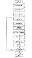
図3から図7を参照して、画像処理方法について説明する。ここでは、多面取り基板に部品の搭載位置を指定する一例について説明する。図3は、本実施の形態の画像処理方法のフローチャートである。図4は、本実施の形態の切り出し処理の一例を示す図である。図5は、本実施の形態のオフセット量の検出処理の一例を示す図である。図6は、本実施の形態の照合処理の一例を示す図である。図7は、本実施の形態の強調表示処理の一例を示す図である。なお、図3のフローチャートは一例を示すものであり、処理の順序が適宜入れ替わってもよい。また、ここでは図2の符号を適宜使用して説明する。 The image processing method will be described with reference to FIGS. Here, an example will be described in which a component mounting position is specified on a multi-panel board. FIG. 3 is a flowchart of the image processing method according to the present embodiment. FIG. 4 is a diagram illustrating an example of the cutout processing according to the present embodiment. FIG. 5 is a diagram illustrating an example of the offset amount detection processing according to the present embodiment. FIG. 6 is a diagram illustrating an example of the matching process according to the present embodiment. FIG. 7 is a diagram illustrating an example of the highlighting process according to the present embodiment. Note that the flowchart of FIG. 3 shows an example, and the order of processing may be changed as appropriate. Further, here, the description will be made using the reference numerals in FIG. 2 as appropriate.
図3に示すように、先ず基板撮像部35によって多面取り基板61が撮像され、第1の取得部41によって基板撮像部35から基板表面の基板画像50が取得される(ステップS01)。次に、高さ計測部34によって多面取り基板61の高さデータが計測され、切り出し部45によって高さデータに基づいて基板画像50から多面取り基板61が存在している部分だけが切り出される(ステップS02)。この場合、高さ計測部34によって多面取り基板61が横切られながら高さデータが計測され、高さ計測部34から切り出し部45に多面取り基板61の高さデータが出力される(図4A参照)。
As shown in FIG. 3, first, the
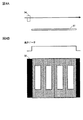
多面取り基板61が存在する位置では高さデータが大きくなり、多面取り基板61が存在しない位置では高さデータが小さくなっている(図4B参照)。このため、高さデータが急激に大きくなった位置から高さデータが急激に小さくなった位置までの範囲で多面取り基板61が存在していると認識される。2点鎖線で示すように多面取り基板61が存在している範囲で、切り出し部45によって基板画像50が切り出されることで、基板画像50の画像サイズが小さくされる。基板画像50から不要な余白部分が取り除かれるため、回路パターンのオフセット量やオフセット角の検出処理時の処理量を低減することが可能になっている。
The height data is large at the position where the
次に、検出部46によって切り出し後の基板画像50から一の単位基板62の回路パターンに対する他の単位基板62の回路パターンのオフセット量が検出される(ステップS03)。この場合、切り出された基板画像50を複製し、正規化相関法によって2つの基板画像50A、50Bを重ね合わせた状態でシフトしながら相関積分される(図5A参照)。初期状態は全ての単位基板62の回路パターンが一致するので相関値(相関積分値)が最も高くなり、初期状態から2つの基板画像50A、50Bがシフトすることで相関値が低くなる。基板画像50Aの1つ目の回路パターンと基板画像50Bの2つ目の回路パターンが一致したタイミングで相関値が再び高くなるが(図5B参照)、両端の単位基板62の回路パターンは重ならないので初期状態よりも相関値は低くなっている。
Next, the offset amount of the circuit pattern of another
この相関値の算出処理が繰り返されることで、基板画像50A、50Bのシフト方向における相関値のピークに基づいて、一の単位基板62の回路パターンに対する他の単位基板62の回路パターンのオフセット量が検出される(図5C参照)。多面取り基板61の複数の単位基板62の回路パターンが同じ向きの場合には、2つの基板画像50A、50Bを縦方向及び横方向にシフトしながら相関値が求められる。なお、図では横方向(X軸方向)の相関積分値のみ図示しているが、実際には縦方向(Y軸方向)の相関積分値も求められる。これにより、相関値のピークに基づいて一の単位基板62の回路パターンに対する他の単位基板62の回路パターンのオフセット量(Δx、Δy)が検出される。
By repeating the process of calculating the correlation value, the offset amount of the circuit pattern of one
また、多面取り基板61の複数の単位基板62の回路パターンが異なる向きの場合には、2つの基板画像50A、50Bを回転方向にシフトしながら相関値が求められる(図5D参照)。これにより、相関値のピークに基づいて一の単位基板62の回路パターンに対する他の単位基板62の回路パターンのオフセット角が検出される。なお、検出部46では、2つの基板画像50A、50Bの縦横方向のシフトと回転方向のシフトを組み合わせて、回路パターンのオフセット量及びオフセット角を検出してもよいし、いずれか一方を使用して回路パターンのオフセット量又はオフセット角を検出してもよい。
When the circuit patterns of the plurality of
次に、底面撮像部37によって部品Pが撮像され、第2の取得部42によって底面撮像部37から部品底面の部品画像51が取得される(ステップS04)。次に、ディスプレイ39に表示された一の単位基板62の基板画像50の任意の箇所がユーザに指定されると、指定箇所を中心した所定範囲に基板画像50の照合範囲59(図6参照)が設定される(ステップS05)。次に、照合部43によって基板画像50の照合範囲59で回路パターンと部品画像51の特徴点が照合される(ステップS06参照)。この場合、基板画像50の照合範囲59に対して部品画像51を縦方向及び横方向に走査しながら相関積分される(図6参照)。
Next, the component P is imaged by the bottom
基板画像50の半田部分と部品画像51の電極部分が一致した位置では相関値(相関積分値)が高くなり、基板画像50の半田部分と部品画像51の電極部分が位置ズレすると相関値が低くなる。基板画像50の複数箇所で相関値が高くなっており、相関値が高い方から上位数箇所が照合箇所として検出される。なお、基板画像50の照合範囲59内に相関値が高い箇所が存在しない場合には、照合範囲59が拡張されて照合箇所が検出されるまで照合処理が継続される。また、基板画像50の半田等の特徴点と部品画像51の電極等の特徴点だけを照合させてもよいし、部品画像51の搭載角度を切り替えて基板画像50に照合させてもよい。また、基板画像50の半田部分と部品画像51の電極部分の明暗が逆転している場合がある。この場合は部品画像51の明暗を反転処理した後で基板画像50との照合処理をさせてもよい。
The correlation value (correlation integral value) increases at a position where the solder portion of the
次に、基板画像50に対して部品画像51が照合されると、表示制御部44によって一の単位基板の基板画像50上の照合箇所が複数の搭載位置の候補としてディスプレイ39で強調表示される(ステップS07)。この場合、基板画像50上の複数の照合箇所に部品Pの外形画像55が重ね合わせられて表示される(図7A参照)。外形画像55としては、例えば、底面画像の部品認識で使用されるテンプレート画像を表裏反転した画像が使用される。また、外形画像55の代わりに塗り潰し画像56(図7B参照)や外形枠画像57(図7C参照)が表示されてもよいし、外形枠画像57に中心線58が追加されて表示されてもよい(図7D参照)。
Next, when the
次に、ディスプレイ39の複数の搭載位置の候補から所望の搭載位置が指定されると(ステップS08)、算出部47によって一の単位基板62の搭載位置と回路パターンのオフセット量から全ての単位基板62の搭載位置が算出される(ステップS09)。例えば、一の単位基板62の搭載位置の搭載座標(X、Y)に対して、他の単位基板のオフセット量(Δx、Δy)を加えることで他の単位基板62の搭載位置が求められる。全ての単位基板62の搭載位置が求められると、生産プログラムに搭載座標が設定されて、搭載位置に対する部品Pの搭載動作が実施される(ステップS10)。
Next, when a desired mounting position is designated from a plurality of mounting position candidates on the display 39 (step S08), the calculating
次に、1つ目の搭載位置の設定が終了すると、全ての搭載位置の設定が終了したか否かが判定される(ステップS11)。そして、全ての搭載位置の設定が終了するまで、ステップS04からステップS11までの処理が繰り返される。このように、生産プログラムに搭載位置をティーチングしながら部品Pの搭載処理が実施される。2枚目以降の多面取り基板61に対する搭載処理では、初回にティーチングした生産プログラムに対して部品Pの搭載順序を最適化することで高速生産することが可能になっている。なお、ここでは基板として多面取り基板を例示して説明したが、この構成に限定されない。通常の基板であれば、上記フローチャートから多面取り基板61の特有のステップS02、ステップS03の処理が省略される。
Next, when the setting of the first mounting position is completed, it is determined whether the setting of all mounting positions is completed (step S11). Then, the processing from step S04 to step S11 is repeated until the setting of all mounting positions is completed. In this way, the mounting process of the component P is performed while teaching the mounting position in the production program. In the mounting process for the second and subsequent
以上のように、本実施の形態の画像処理装置40では、部品底面の特徴点と基板表面の回路パターンの照合結果に応じて、ディスプレイ39に映された基板画像50上で部品Pの搭載位置が強調表示される。基板画像50上で強調表示された搭載位置を指定することで、CADデータを使用することなく、生産プログラムに搭載位置のティーチングを行うことができる。よって、部品Pの搭載位置を容易に指定することができ、作業負担を軽減する共に作業時間を短縮することができる。
As described above, in the
なお、本実施の形態において、照合部は、部品画像と基板画像の相関積分によって照合する構成にしたが、この構成に限定されない。照合部は、部品画像の特徴点と基板画像の回路パターンを照合可能であれば、どのように構成されてもよい。 In the present embodiment, the collation unit is configured to perform the collation by the correlation integration between the component image and the board image, but is not limited to this configuration. The matching unit may be configured in any manner as long as the feature points of the component image can be compared with the circuit pattern of the board image.
また、本実施の形態において、照合部は、相関積分値のピークから照合位置を検出する構成にしたが、この構成に限定されない。照合部は、閾値以上の相関積分値から照合位置を検出してもよい。 Further, in the present embodiment, the matching unit detects the matching position from the peak of the correlation integral value, but is not limited to this configuration. The collation unit may detect the collation position from the correlation integral value equal to or greater than the threshold.
また、本実施の形態において、検出部は、2つの基板画像の相関積分によって一の単位基板の回路パターンに対する他の単位基板の回路パターンのオフセット量を検出する構成にしたが、この構成に限定されない。検出部は、一の単位基板の回路パターンに対する他の単位基板の回路パターンのオフセット量を検出可能であれば、どのように構成されてもよい。 Further, in the present embodiment, the detection unit is configured to detect the offset amount of the circuit pattern of one unit substrate with respect to the circuit pattern of another unit substrate by correlation integration of the two substrate images, but is not limited to this configuration. Not done. The detection unit may be configured in any manner as long as it can detect the offset amount of the circuit pattern of another unit substrate with respect to the circuit pattern of one unit substrate.
また、本実施の形態において、検出部は、相関積分値のピークからオフセット量を検出する構成にしたが、この構成に限定されない。検出部は、閾値以上の相関積分値に基づいて回路パターン同士の照合位置を求めてオフセット量を検出してもよい。 Further, in the present embodiment, the detection unit is configured to detect the offset amount from the peak of the correlation integral value, but is not limited to this configuration. The detecting unit may detect the offset amount by obtaining a matching position between the circuit patterns based on the correlation integral value equal to or larger than the threshold value.
また、本実施の形態において、表示制御部は、照合部の照合結果で相関が高い方から上位数箇所を搭載位置の候補として強調表示する構成にしたが、この構成に限定されない。表示制御部は、照合部の照合結果の中で最も相関が高い照合箇所を搭載位置として強調表示してもよい。 Further, in the present embodiment, the display control unit has a configuration in which the top several places with the highest correlation in the collation result of the collation unit are highlighted as mounting position candidates, but the present invention is not limited to this configuration. The display control unit may highlight the matching location having the highest correlation among the matching results of the matching unit as the mounting position.
また、本実施の形態において、画像処理装置が切り出し部、検出部、算出部を備える構成にしたが、この構成に限定されない。多面取り基板ではない基板に部品の搭載位置を指定する場合には、切り出し部、検出部、算出部を備えていなくてもよい。 Further, in the present embodiment, the image processing apparatus is configured to include the cutout unit, the detection unit, and the calculation unit; however, the configuration is not limited to this. When a component mounting position is specified on a board that is not a multi-panel board, the cutout section, the detection section, and the calculation section need not be provided.
また、本実施の形態において、基板画像の任意の箇所を指定して照合範囲を設定する構成にしたが、この構成に限定されない。例えば、小型基板の場合には、基板画像に照合範囲を設定しなくてもよい。 Further, in the present embodiment, the configuration in which an arbitrary portion of the board image is specified to set the collation range is set, but the present invention is not limited to this configuration. For example, in the case of a small board, the collation range need not be set in the board image.
また、本実施の形態において、画像処理装置が実装装置に組み込まれる構成について説明したが、この構成に限定されない。画像処理装置は、実装装置とは別体に設けられていてもよい。 Further, in the present embodiment, the configuration in which the image processing apparatus is incorporated in the mounting apparatus has been described, but the present invention is not limited to this configuration. The image processing device may be provided separately from the mounting device.
また、本実施の形態において、第1の取得部は基板撮像部から基板画像を取得する構成にしたが、この構成に限定されない。第1の取得部は、基板画像を取得可能な構成であればよく、例えば、事前に外部記憶媒体に記憶した基板画像を外部記憶媒体から取得してもよい。 Further, in the present embodiment, the first acquisition unit is configured to acquire the board image from the board imaging unit, but is not limited to this configuration. The first acquisition unit only needs to be capable of acquiring a board image. For example, the first acquisition unit may acquire a board image stored in an external storage medium in advance from the external storage medium.
また、本実施の形態において、第2の取得部は底面撮像部から部品画像を取得する構成にしたが、この構成に限定されない。第2の取得部は、部品画像を取得可能な構成であればよく、例えば、事前に外部記憶媒体に記憶した部品画像を外部記憶媒体から取得してもよい。 Further, in the present embodiment, the second acquisition unit is configured to acquire the component image from the bottom surface imaging unit, but is not limited to this configuration. The second acquisition unit may have any configuration as long as it can acquire a component image. For example, the second acquisition unit may acquire a component image stored in advance in an external storage medium from the external storage medium.
また、本実施の形態において、実装装置に画像処理装置を備える構成について説明したが、画像処理装置は撮像装置を備えた他の装置に適用可能である。 Further, in the present embodiment, the configuration in which the mounting device includes the image processing device has been described, but the image processing device is applicable to another device including the imaging device.
また、本実施の形態のプログラムは記憶媒体に記憶されてもよい。記憶媒体は、特に限定されないが、光ディスク、光磁気ディスク、フラッシュメモリ等の非一過性の記録媒体であってもよい。 Further, the program of the present embodiment may be stored in a storage medium. The storage medium is not particularly limited, but may be a non-transitory storage medium such as an optical disk, a magneto-optical disk, and a flash memory.
また、本発明の実施の形態及び変形例を説明したが、本発明の他の実施の形態として、上記実施の形態及び変形例を全体的又は部分的に組み合わせたものでもよい。 Although the embodiment and the modification of the present invention have been described, another embodiment of the present invention may be a combination of the above embodiment and the modification in whole or in part.
また、本発明の実施の形態は上記の実施の形態及び変形例に限定されるものではなく、本発明の技術的思想の趣旨を逸脱しない範囲において様々に変更、置換、変形されてもよい。さらには、技術の進歩又は派生する別技術によって、本発明の技術的思想を別の仕方で実現することができれば、その方法を用いて実施されてもよい。したがって、特許請求の範囲は、本発明の技術的思想の範囲内に含まれ得る全ての実施態様をカバーしている。 Further, the embodiments of the present invention are not limited to the above-described embodiments and modified examples, and may be variously changed, replaced, or modified without departing from the spirit of the technical idea of the present invention. Further, if the technical idea of the present invention can be realized in another way by the advance of the technology or another derived technology, the method may be implemented using the method. Therefore, the claims cover all embodiments that can be included in the scope of the technical idea of the present invention.
さらに、上記実施の形態では、表面に回路パターンを形成した基板が撮像されて、当該基板に対する部品の搭載位置をディスプレイに指定可能に表示させる画像処理装置であって、基板表面を撮像した基板画像を取得する第1の取得部と、部品底面を撮像した部品画像を取得する第2の取得部と、部品画像の特徴点を基板画像の回路パターンに照合する照合部と、基板画像上の照合箇所を搭載位置として強調表示する表示制御部とを備えたことを特徴とする。この構成によれば、部品底面の特徴点と基板表面の回路パターンの照合結果に応じて、ディスプレイに映された基板画像上で部品の搭載位置が強調表示される。基板画像上で強調表示された搭載位置を指定することで、CADデータを使用することなく、生産プログラムに搭載位置のティーチングを行うことができる。よって、部品の搭載位置を容易に指定することができ、ユーザの作業負担を軽減する共に作業時間を短縮することができる。 Furthermore, in the above-described embodiment, the image processing apparatus is configured to capture an image of a substrate on which a circuit pattern is formed on a surface, and to display a mounting position of a component on the substrate so as to be specified on a display. A first acquisition unit for acquiring a component image obtained by imaging the bottom surface of the component, a collation unit for collating feature points of the component image with a circuit pattern of the board image, and a collation on the board image. A display control unit that highlights the location as a mounting position. According to this configuration, the mounting position of the component is highlighted on the board image displayed on the display in accordance with the result of matching the feature point on the bottom surface of the component with the circuit pattern on the board surface. By specifying the mounting position highlighted on the board image, the mounting position can be taught in the production program without using CAD data. Therefore, the mounting position of the component can be easily specified, and the work load on the user can be reduced, and the work time can be shortened.
以上説明したように、本発明は、部品の搭載位置を容易に指定することができるという効果を有し、特に、基板に部品を実装する画像処理装置、実装装置、画像処理方法、プログラムに有用である。 As described above, the present invention has an effect that a component mounting position can be easily specified, and is particularly useful for an image processing apparatus, a mounting apparatus, an image processing method, and a program for mounting a component on a board. It is.
1 :実装装置
30:搭載ヘッド
34:高さ計測部(計測部)
39:ディスプレイ
40:画像処理装置
41:第1の取得部
42:第2の取得部
43:照合部
44:表示制御部
45:切り出し部
46:検出部
47:算出部
50:基板画像
51:部品画像
60:基板
61:多面取り基板
62:単位基板
P :部品
1: mounting device 30: mounting head 34: height measuring unit (measuring unit)
39: display 40: image processing device 41: first acquisition unit 42: second acquisition unit 43: collation unit 44: display control unit 45: cutout unit 46: detection unit 47: calculation unit 50: board image 51: component Image 60: board 61: multiple board 62: unit board P: component
Claims (10)
基板表面を撮像した基板画像を取得する第1の取得部と、
部品底面を撮像した部品画像を取得する第2の取得部と、
部品画像の特徴点を基板画像の回路パターンに照合する照合部と、
基板画像上の照合箇所を搭載位置として強調表示する表示制御部とを備えたことを特徴とする画像処理装置。 An image processing apparatus in which a substrate having a circuit pattern formed on its surface is imaged, and a mounting position of a component on the substrate is displayed so as to be specified on a display,
A first acquisition unit that acquires a board image of the board surface,
A second acquisition unit for acquiring a component image obtained by imaging the component bottom surface;
A matching unit that matches feature points of the component image with a circuit pattern of the board image,
An image processing apparatus comprising: a display control unit that highlights a collation location on a board image as a mounting position.
一の単位基板の回路パターンに対する他の単位基板の回路パターンのオフセット量を検出する検出部と、
一の単位基板の搭載位置と回路パターンのオフセット量から他の単位基板の搭載位置を求める算出部とを備えることを特徴とする請求項1から請求項3のいずれかに記載の画像処理装置。 The board is a multi-panel board composed of a plurality of unit boards having the same circuit pattern,
A detection unit that detects an offset amount of a circuit pattern of another unit substrate with respect to a circuit pattern of one unit substrate,
4. The image processing apparatus according to claim 1, further comprising: a calculation unit configured to calculate a mounting position of another unit substrate from a mounting position of one unit substrate and an offset amount of a circuit pattern. 5.
前記検出部は、切り出し後の2つの基板画像をシフトしながら回路パターンの相関を求めることを特徴とする請求項4から請求項6のいずれかに記載の画像処理装置。 A cutout unit that cuts out a board image based on height data measured while traversing the multi-faced board by the measurement unit,
The image processing apparatus according to claim 4, wherein the detection unit calculates the correlation between the circuit patterns while shifting the two board images after the clipping.
前記画像処理装置で指定された搭載位置に部品を搭載する搭載ヘッドとを備えたことを特徴とする実装装置。 An image processing device according to any one of claims 1 to 7,
A mounting head for mounting a component at a mounting position designated by the image processing apparatus.
基板表面を撮像した基板画像を取得するステップと、
部品底面を撮像した部品画像を取得するステップと、
部品画像の特徴点を基板画像の回路パターンに照合するステップと、
基板画像上の照合箇所を搭載位置として強調表示するステップとを有することを特徴とする画像処理方法。 An image processing method in which a substrate having a circuit pattern formed on its surface is imaged, and a mounting position of a component on the substrate is displayed so as to be specified on a display,
Obtaining a board image of the board surface,
Acquiring a component image of the bottom surface of the component,
Matching feature points of the part image with the circuit pattern of the board image;
Highlighting the collation location on the board image as the mounting position.
基板表面を撮像した基板画像を取得するステップと、
部品底面を撮像した部品画像を取得するステップと、
部品画像の特徴点を基板画像の回路パターンに照合するステップと、
基板画像上の照合箇所を搭載位置として強調表示するステップとを前記画像処理装置に実行させることを特徴とするプログラム。 A program of an image processing apparatus, in which a substrate on which a circuit pattern is formed is imaged, and a mounting position of a component on the substrate is displayed so as to be specified on a display,
Obtaining a board image of the board surface,
Acquiring a component image of the bottom surface of the component,
Matching feature points of the part image with the circuit pattern of the board image;
Causing the image processing apparatus to execute a step of highlighting a collation location on the board image as a mounting position.
Priority Applications (2)
| Application Number | Priority Date | Filing Date | Title |
|---|---|---|---|
| JP2018125868A JP7126880B2 (en) | 2018-07-02 | 2018-07-02 | Image processing device, mounting device, image processing method, program |
| CN201910591424.2A CN110678060B (en) | 2018-07-02 | 2019-07-02 | Image processing apparatus, mounting apparatus, image processing method, and storage medium |
Applications Claiming Priority (1)
| Application Number | Priority Date | Filing Date | Title |
|---|---|---|---|
| JP2018125868A JP7126880B2 (en) | 2018-07-02 | 2018-07-02 | Image processing device, mounting device, image processing method, program |
Publications (2)
| Publication Number | Publication Date |
|---|---|
| JP2020004923A true JP2020004923A (en) | 2020-01-09 |
| JP7126880B2 JP7126880B2 (en) | 2022-08-29 |
Family
ID=69068611
Family Applications (1)
| Application Number | Title | Priority Date | Filing Date |
|---|---|---|---|
| JP2018125868A Active JP7126880B2 (en) | 2018-07-02 | 2018-07-02 | Image processing device, mounting device, image processing method, program |
Country Status (2)
| Country | Link |
|---|---|
| JP (1) | JP7126880B2 (en) |
| CN (1) | CN110678060B (en) |
Citations (4)
| Publication number | Priority date | Publication date | Assignee | Title |
|---|---|---|---|---|
| JP2012069617A (en) * | 2010-09-22 | 2012-04-05 | Fuji Mach Mfg Co Ltd | Component attachment coordinate generating device and component attachment coordinate generating method |
| JP2014029962A (en) * | 2012-07-31 | 2014-02-13 | Fuji Mach Mfg Co Ltd | Mounting machine |
| WO2016006076A1 (en) * | 2014-07-10 | 2016-01-14 | 富士機械製造株式会社 | Method for producing component placement coordinates and device for producing component placement coordinates |
| JP2018029161A (en) * | 2016-08-19 | 2018-02-22 | メイショウ株式会社 | Image processing system for component mounting machine |
Family Cites Families (4)
| Publication number | Priority date | Publication date | Assignee | Title |
|---|---|---|---|---|
| JP2000323897A (en) * | 1999-05-11 | 2000-11-24 | Sony Corp | Equipment for positioning support pin for wiring board |
| WO2009093445A1 (en) * | 2008-01-25 | 2009-07-30 | Panasonic Corporation | Inspection device and inspection method |
| CN101776964A (en) * | 2010-02-25 | 2010-07-14 | 昆山锐芯微电子有限公司 | Input system and method for controlling movement of object on display screen |
| JP6389651B2 (en) * | 2013-09-10 | 2018-09-12 | Juki株式会社 | Inspection method, mounting method, and mounting apparatus |
-
2018
- 2018-07-02 JP JP2018125868A patent/JP7126880B2/en active Active
-
2019
- 2019-07-02 CN CN201910591424.2A patent/CN110678060B/en active Active
Patent Citations (4)
| Publication number | Priority date | Publication date | Assignee | Title |
|---|---|---|---|---|
| JP2012069617A (en) * | 2010-09-22 | 2012-04-05 | Fuji Mach Mfg Co Ltd | Component attachment coordinate generating device and component attachment coordinate generating method |
| JP2014029962A (en) * | 2012-07-31 | 2014-02-13 | Fuji Mach Mfg Co Ltd | Mounting machine |
| WO2016006076A1 (en) * | 2014-07-10 | 2016-01-14 | 富士機械製造株式会社 | Method for producing component placement coordinates and device for producing component placement coordinates |
| JP2018029161A (en) * | 2016-08-19 | 2018-02-22 | メイショウ株式会社 | Image processing system for component mounting machine |
Also Published As
| Publication number | Publication date |
|---|---|
| CN110678060B (en) | 2023-05-23 |
| CN110678060A (en) | 2020-01-10 |
| JP7126880B2 (en) | 2022-08-29 |
Similar Documents
| Publication | Publication Date | Title |
|---|---|---|
| JP2008270696A (en) | Component mounting position correcting method and component mounting apparatus | |
| US10721849B2 (en) | Component data handling device and component mounting system | |
| WO2007033349A1 (en) | Pick and place machine with improved component pick image processing | |
| CN107926154B (en) | Component mounting apparatus | |
| JP6646916B2 (en) | Image processing apparatus and image processing method for substrate | |
| JP2017150927A (en) | Inspection device, mounted device, inspection method, and program | |
| JP6734868B2 (en) | Image processing apparatus and image processing method for substrate | |
| JP2008021946A (en) | Packaging machine | |
| US11210764B2 (en) | Apparatus for performing work on substrate | |
| CN106455478B (en) | Inspection apparatus, mounting apparatus, and inspection method | |
| JP7126880B2 (en) | Image processing device, mounting device, image processing method, program | |
| JP4707607B2 (en) | Image acquisition method for component recognition data creation and component mounter | |
| JP3434004B2 (en) | Component recognition device and component mounting device | |
| JP6706695B2 (en) | Coordinate data generation device and coordinate data generation method | |
| EP3370493B1 (en) | Base plate position searching device and component mounting machine | |
| JP7427652B2 (en) | A system and component mounting system consisting of a mounting data creation support device, a mounting data creation support method, a visual inspection machine, and a control device. | |
| JP7253476B2 (en) | Component recognition data creation method and component recognition data creation program | |
| JP6621639B2 (en) | Image processing apparatus for substrates | |
| JP2005116869A (en) | Reference mark position detector and reference mark position detection program | |
| JP2017130592A (en) | Component data handling device, component data handling method, and component mounting system | |
| JP2020009938A (en) | Image processing apparatus, mounting apparatus, image processing method, and program | |
| JP2019075475A (en) | Component mounting device | |
| WO2019058475A1 (en) | Shape data analogy determination device | |
| JP4681984B2 (en) | Component positioning method and apparatus | |
| JP2023110671A (en) | Image processing device and image processing method |
Legal Events
| Date | Code | Title | Description |
|---|---|---|---|
| A621 | Written request for application examination |
Free format text: JAPANESE INTERMEDIATE CODE: A621 Effective date: 20210617 |
|
| A977 | Report on retrieval |
Free format text: JAPANESE INTERMEDIATE CODE: A971007 Effective date: 20220428 |
|
| A131 | Notification of reasons for refusal |
Free format text: JAPANESE INTERMEDIATE CODE: A131 Effective date: 20220510 |
|
| A521 | Request for written amendment filed |
Free format text: JAPANESE INTERMEDIATE CODE: A523 Effective date: 20220707 |
|
| TRDD | Decision of grant or rejection written | ||
| A01 | Written decision to grant a patent or to grant a registration (utility model) |
Free format text: JAPANESE INTERMEDIATE CODE: A01 Effective date: 20220802 |
|
| A61 | First payment of annual fees (during grant procedure) |
Free format text: JAPANESE INTERMEDIATE CODE: A61 Effective date: 20220817 |
|
| R150 | Certificate of patent or registration of utility model |
Ref document number: 7126880 Country of ref document: JP Free format text: JAPANESE INTERMEDIATE CODE: R150 |