JP2019079030A - 露光装置および物品の製造方法 - Google Patents
露光装置および物品の製造方法 Download PDFInfo
- Publication number
- JP2019079030A JP2019079030A JP2018146251A JP2018146251A JP2019079030A JP 2019079030 A JP2019079030 A JP 2019079030A JP 2018146251 A JP2018146251 A JP 2018146251A JP 2018146251 A JP2018146251 A JP 2018146251A JP 2019079030 A JP2019079030 A JP 2019079030A
- Authority
- JP
- Japan
- Prior art keywords
- light
- substrate
- exposure
- receiving element
- exposure apparatus
- Prior art date
- Legal status (The legal status is an assumption and is not a legal conclusion. Google has not performed a legal analysis and makes no representation as to the accuracy of the status listed.)
- Pending
Links
- 238000004519 manufacturing process Methods 0.000 title description 11
- 239000000758 substrate Substances 0.000 claims abstract description 102
- 230000003287 optical effect Effects 0.000 claims abstract description 92
- 230000008859 change Effects 0.000 claims abstract description 10
- 238000000034 method Methods 0.000 claims description 13
- 238000005286 illumination Methods 0.000 claims description 8
- 239000002184 metal Substances 0.000 claims description 4
- 230000000903 blocking effect Effects 0.000 claims 7
- 230000001678 irradiating effect Effects 0.000 claims 1
- 230000004907 flux Effects 0.000 abstract description 13
- 238000003384 imaging method Methods 0.000 description 26
- 238000001514 detection method Methods 0.000 description 13
- 230000004048 modification Effects 0.000 description 13
- 238000012986 modification Methods 0.000 description 13
- 230000007423 decrease Effects 0.000 description 6
- 101100335694 Oryza sativa subsp. japonica G1L6 gene Proteins 0.000 description 4
- 238000010586 diagram Methods 0.000 description 4
- 238000012545 processing Methods 0.000 description 4
- 230000006872 improvement Effects 0.000 description 3
- 210000003644 lens cell Anatomy 0.000 description 3
- 239000000463 material Substances 0.000 description 3
- 238000012937 correction Methods 0.000 description 2
- 230000007261 regionalization Effects 0.000 description 2
- 239000004065 semiconductor Substances 0.000 description 2
- 230000009471 action Effects 0.000 description 1
- 230000015572 biosynthetic process Effects 0.000 description 1
- 239000003795 chemical substances by application Substances 0.000 description 1
- 238000007796 conventional method Methods 0.000 description 1
- 230000008021 deposition Effects 0.000 description 1
- 230000000694 effects Effects 0.000 description 1
- 238000005530 etching Methods 0.000 description 1
- 238000010606 normalization Methods 0.000 description 1
- 230000003647 oxidation Effects 0.000 description 1
- 238000007254 oxidation reaction Methods 0.000 description 1
- 238000004806 packaging method and process Methods 0.000 description 1
- 230000008569 process Effects 0.000 description 1
Images


Classifications
-
- G—PHYSICS
- G03—PHOTOGRAPHY; CINEMATOGRAPHY; ANALOGOUS TECHNIQUES USING WAVES OTHER THAN OPTICAL WAVES; ELECTROGRAPHY; HOLOGRAPHY
- G03F—PHOTOMECHANICAL PRODUCTION OF TEXTURED OR PATTERNED SURFACES, e.g. FOR PRINTING, FOR PROCESSING OF SEMICONDUCTOR DEVICES; MATERIALS THEREFOR; ORIGINALS THEREFOR; APPARATUS SPECIALLY ADAPTED THEREFOR
- G03F7/00—Photomechanical, e.g. photolithographic, production of textured or patterned surfaces, e.g. printing surfaces; Materials therefor, e.g. comprising photoresists; Apparatus specially adapted therefor
- G03F7/70—Microphotolithographic exposure; Apparatus therefor
- G03F7/70483—Information management; Active and passive control; Testing; Wafer monitoring, e.g. pattern monitoring
- G03F7/70605—Workpiece metrology
- G03F7/70616—Monitoring the printed patterns
- G03F7/70641—Focus
-
- G—PHYSICS
- G03—PHOTOGRAPHY; CINEMATOGRAPHY; ANALOGOUS TECHNIQUES USING WAVES OTHER THAN OPTICAL WAVES; ELECTROGRAPHY; HOLOGRAPHY
- G03F—PHOTOMECHANICAL PRODUCTION OF TEXTURED OR PATTERNED SURFACES, e.g. FOR PRINTING, FOR PROCESSING OF SEMICONDUCTOR DEVICES; MATERIALS THEREFOR; ORIGINALS THEREFOR; APPARATUS SPECIALLY ADAPTED THEREFOR
- G03F9/00—Registration or positioning of originals, masks, frames, photographic sheets or textured or patterned surfaces, e.g. automatically
- G03F9/70—Registration or positioning of originals, masks, frames, photographic sheets or textured or patterned surfaces, e.g. automatically for microlithography
- G03F9/7003—Alignment type or strategy, e.g. leveling, global alignment
- G03F9/7023—Aligning or positioning in direction perpendicular to substrate surface
- G03F9/7026—Focusing
-
- G—PHYSICS
- G03—PHOTOGRAPHY; CINEMATOGRAPHY; ANALOGOUS TECHNIQUES USING WAVES OTHER THAN OPTICAL WAVES; ELECTROGRAPHY; HOLOGRAPHY
- G03F—PHOTOMECHANICAL PRODUCTION OF TEXTURED OR PATTERNED SURFACES, e.g. FOR PRINTING, FOR PROCESSING OF SEMICONDUCTOR DEVICES; MATERIALS THEREFOR; ORIGINALS THEREFOR; APPARATUS SPECIALLY ADAPTED THEREFOR
- G03F7/00—Photomechanical, e.g. photolithographic, production of textured or patterned surfaces, e.g. printing surfaces; Materials therefor, e.g. comprising photoresists; Apparatus specially adapted therefor
- G03F7/70—Microphotolithographic exposure; Apparatus therefor
- G03F7/70058—Mask illumination systems
- G03F7/70091—Illumination settings, i.e. intensity distribution in the pupil plane or angular distribution in the field plane; On-axis or off-axis settings, e.g. annular, dipole or quadrupole settings; Partial coherence control, i.e. sigma or numerical aperture [NA]
-
- G—PHYSICS
- G02—OPTICS
- G02B—OPTICAL ELEMENTS, SYSTEMS OR APPARATUS
- G02B7/00—Mountings, adjusting means, or light-tight connections, for optical elements
- G02B7/28—Systems for automatic generation of focusing signals
- G02B7/30—Systems for automatic generation of focusing signals using parallactic triangle with a base line
- G02B7/32—Systems for automatic generation of focusing signals using parallactic triangle with a base line using active means, e.g. light emitter
-
- G—PHYSICS
- G02—OPTICS
- G02B—OPTICAL ELEMENTS, SYSTEMS OR APPARATUS
- G02B7/00—Mountings, adjusting means, or light-tight connections, for optical elements
- G02B7/28—Systems for automatic generation of focusing signals
- G02B7/40—Systems for automatic generation of focusing signals using time delay of the reflected waves, e.g. of ultrasonic waves
-
- G—PHYSICS
- G03—PHOTOGRAPHY; CINEMATOGRAPHY; ANALOGOUS TECHNIQUES USING WAVES OTHER THAN OPTICAL WAVES; ELECTROGRAPHY; HOLOGRAPHY
- G03F—PHOTOMECHANICAL PRODUCTION OF TEXTURED OR PATTERNED SURFACES, e.g. FOR PRINTING, FOR PROCESSING OF SEMICONDUCTOR DEVICES; MATERIALS THEREFOR; ORIGINALS THEREFOR; APPARATUS SPECIALLY ADAPTED THEREFOR
- G03F7/00—Photomechanical, e.g. photolithographic, production of textured or patterned surfaces, e.g. printing surfaces; Materials therefor, e.g. comprising photoresists; Apparatus specially adapted therefor
- G03F7/70—Microphotolithographic exposure; Apparatus therefor
- G03F7/70058—Mask illumination systems
- G03F7/70091—Illumination settings, i.e. intensity distribution in the pupil plane or angular distribution in the field plane; On-axis or off-axis settings, e.g. annular, dipole or quadrupole settings; Partial coherence control, i.e. sigma or numerical aperture [NA]
- G03F7/70116—Off-axis setting using a programmable means, e.g. liquid crystal display [LCD], digital micromirror device [DMD] or pupil facets
-
- G—PHYSICS
- G03—PHOTOGRAPHY; CINEMATOGRAPHY; ANALOGOUS TECHNIQUES USING WAVES OTHER THAN OPTICAL WAVES; ELECTROGRAPHY; HOLOGRAPHY
- G03F—PHOTOMECHANICAL PRODUCTION OF TEXTURED OR PATTERNED SURFACES, e.g. FOR PRINTING, FOR PROCESSING OF SEMICONDUCTOR DEVICES; MATERIALS THEREFOR; ORIGINALS THEREFOR; APPARATUS SPECIALLY ADAPTED THEREFOR
- G03F7/00—Photomechanical, e.g. photolithographic, production of textured or patterned surfaces, e.g. printing surfaces; Materials therefor, e.g. comprising photoresists; Apparatus specially adapted therefor
- G03F7/70—Microphotolithographic exposure; Apparatus therefor
- G03F7/70058—Mask illumination systems
- G03F7/702—Reflective illumination, i.e. reflective optical elements other than folding mirrors, e.g. extreme ultraviolet [EUV] illumination systems
-
- G—PHYSICS
- G03—PHOTOGRAPHY; CINEMATOGRAPHY; ANALOGOUS TECHNIQUES USING WAVES OTHER THAN OPTICAL WAVES; ELECTROGRAPHY; HOLOGRAPHY
- G03F—PHOTOMECHANICAL PRODUCTION OF TEXTURED OR PATTERNED SURFACES, e.g. FOR PRINTING, FOR PROCESSING OF SEMICONDUCTOR DEVICES; MATERIALS THEREFOR; ORIGINALS THEREFOR; APPARATUS SPECIALLY ADAPTED THEREFOR
- G03F7/00—Photomechanical, e.g. photolithographic, production of textured or patterned surfaces, e.g. printing surfaces; Materials therefor, e.g. comprising photoresists; Apparatus specially adapted therefor
- G03F7/70—Microphotolithographic exposure; Apparatus therefor
- G03F7/70216—Mask projection systems
- G03F7/70258—Projection system adjustments, e.g. adjustments during exposure or alignment during assembly of projection system
-
- G—PHYSICS
- G03—PHOTOGRAPHY; CINEMATOGRAPHY; ANALOGOUS TECHNIQUES USING WAVES OTHER THAN OPTICAL WAVES; ELECTROGRAPHY; HOLOGRAPHY
- G03F—PHOTOMECHANICAL PRODUCTION OF TEXTURED OR PATTERNED SURFACES, e.g. FOR PRINTING, FOR PROCESSING OF SEMICONDUCTOR DEVICES; MATERIALS THEREFOR; ORIGINALS THEREFOR; APPARATUS SPECIALLY ADAPTED THEREFOR
- G03F7/00—Photomechanical, e.g. photolithographic, production of textured or patterned surfaces, e.g. printing surfaces; Materials therefor, e.g. comprising photoresists; Apparatus specially adapted therefor
- G03F7/70—Microphotolithographic exposure; Apparatus therefor
- G03F7/70216—Mask projection systems
- G03F7/70283—Mask effects on the imaging process
- G03F7/70291—Addressable masks, e.g. spatial light modulators [SLMs], digital micro-mirror devices [DMDs] or liquid crystal display [LCD] patterning devices
-
- G—PHYSICS
- G03—PHOTOGRAPHY; CINEMATOGRAPHY; ANALOGOUS TECHNIQUES USING WAVES OTHER THAN OPTICAL WAVES; ELECTROGRAPHY; HOLOGRAPHY
- G03F—PHOTOMECHANICAL PRODUCTION OF TEXTURED OR PATTERNED SURFACES, e.g. FOR PRINTING, FOR PROCESSING OF SEMICONDUCTOR DEVICES; MATERIALS THEREFOR; ORIGINALS THEREFOR; APPARATUS SPECIALLY ADAPTED THEREFOR
- G03F7/00—Photomechanical, e.g. photolithographic, production of textured or patterned surfaces, e.g. printing surfaces; Materials therefor, e.g. comprising photoresists; Apparatus specially adapted therefor
- G03F7/70—Microphotolithographic exposure; Apparatus therefor
- G03F7/70216—Mask projection systems
- G03F7/70358—Scanning exposure, i.e. relative movement of patterned beam and workpiece during imaging
-
- G—PHYSICS
- G03—PHOTOGRAPHY; CINEMATOGRAPHY; ANALOGOUS TECHNIQUES USING WAVES OTHER THAN OPTICAL WAVES; ELECTROGRAPHY; HOLOGRAPHY
- G03F—PHOTOMECHANICAL PRODUCTION OF TEXTURED OR PATTERNED SURFACES, e.g. FOR PRINTING, FOR PROCESSING OF SEMICONDUCTOR DEVICES; MATERIALS THEREFOR; ORIGINALS THEREFOR; APPARATUS SPECIALLY ADAPTED THEREFOR
- G03F7/00—Photomechanical, e.g. photolithographic, production of textured or patterned surfaces, e.g. printing surfaces; Materials therefor, e.g. comprising photoresists; Apparatus specially adapted therefor
- G03F7/70—Microphotolithographic exposure; Apparatus therefor
- G03F7/708—Construction of apparatus, e.g. environment aspects, hygiene aspects or materials
- G03F7/7085—Detection arrangement, e.g. detectors of apparatus alignment possibly mounted on wafers, exposure dose, photo-cleaning flux, stray light, thermal load
-
- H—ELECTRICITY
- H01—ELECTRIC ELEMENTS
- H01L—SEMICONDUCTOR DEVICES NOT COVERED BY CLASS H10
- H01L21/00—Processes or apparatus adapted for the manufacture or treatment of semiconductor or solid state devices or of parts thereof
- H01L21/02—Manufacture or treatment of semiconductor devices or of parts thereof
- H01L21/027—Making masks on semiconductor bodies for further photolithographic processing not provided for in group H01L21/18 or H01L21/34
Abstract
Description
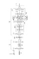
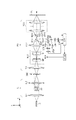
図1を用いて、本実施形態に係る照明光学系IL及び投影光学系POを含む露光装置の構成を説明する。
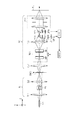
図2を用いて本発明の第2実施形態に係る露光装置について説明する。第1実施形態に係る露光装置では、投影光学系POの光路を遮光するピンホールPH1を用いてデフォーカス量の検出及びフォーカス制御を行う。第2実施形態に係る露光装置では、投影光学系POの光路中に設けられたビームスプリッタBS1aによって反射された光の光路中に、複数の開口を有するピンホールPH2を配置している。以下、第1実施形態との差異について説明する。なお、第1実施形態と同一の構成については説明を割愛する。
図3を用いて本発明の第3実施形態に係る露光装置について説明する。第2実施形態として、投影光学系POの光路中に設けられたビームスプリッタBS1aによって反射された光の光路中に、複数の開口を有するピンホールPH2を配置する構成を説明した。本実施形態では、投影光学系POよりも光源LS側に設けられたビームスプリッタBS3によって反射された光の光路中に、複数の開口を有するピンホールPH3を配置している。以下、第1実施形態及び第2実施形態との差異について説明する。なお、第1実施形態及び第2実施形態と同一の構成については説明を割愛する。
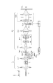
図4を用いて本発明の第4実施形態に係る露光装置について説明する。本実施形態では、照明光学系ILと投影光学系POを含む露光ユニットEUとは別に、スポット光の集光位置と基板PL面との位置ずれを示すデフォーカス量の検出を行うための光学ユニットOUを設けている。なお露光ユニットEUの構成はこれまでの実施形態において説明した構成と同一であるため、露光ユニットEUに関する説明は割愛する。
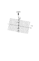
図5は、基板上の走査露光の概要を示す図である。DMDはXY平面内に配置された複数のマイクロミラーから構成され、図5における各点は、DMDを構成するマイクロミラーによって形成されたスポット光を示している。
図8は、第2実施形態に係る露光装置の変形例1を示す図である。第2実施形態における露光装置との相違点は、ピンホールPH2の配置場所にある。変形例1では、結像レンズL1aによる集光面BPから所定量だけ離してピンホールPH2を配置している。
図10は、第2実施形態に係る露光装置の変形例2を示す図である。変形例2では、結像レンズL1aを透過した光束をビームスプリッタBS2により、透過光束と反射光束に分けている。そして、ビームスプリッタBS2を透過した透過光束が、ピンホールPH2a、結像レンズL2aを透過して受光素子LR2aに集光するような光学配置としている。また、ビームスプリッタBS2にて反射された反射光束が、ピンホールPH2b、結像レンズL2bを透過して受光素子LR2bに集光するような光学配置としている。制御部CTRは、受光素子LR2a及び受光素子LR2bからの情報に基づいてアクチュエータAFD2に対して駆動信号を送信する。
なお、基板PLを投影光学系POの光軸方向に駆動させることにより、デフォーカス量を変化させるフォーカス制御を行っても良い。
本発明の実施形態にかかる物品の製造方法は、例えば、半導体デバイス等のマイクロデバイスや微細構造を有する素子等の物品を製造するのに好適である。本実施形態の物品の製造方法は、基板に塗布された感光剤に上記の露光装置を用いて潜像パターンを形成する工程(基板を露光する工程)と、かかる工程で潜像パターンが形成された基板を現像する工程とを含む。さらに、かかる製造方法は、他の周知の工程(酸化、成膜、蒸着、ドーピング、平坦化、エッチング、レジスト剥離、ダイシング、ボンディング、パッケージング等)を含む。本実施形態の物品の製造方法は、従来の方法に比べて、物品の性能・品質・生産性・生産コストの少なくとも1つにおいて有利である。
PL 基板
PH 遮光部材
LR 受光素子
CTR 制御部
Claims (15)
- 基板にパターンを形成するための露光光を基板上に投影する投影光学系と、
前記基板において反射された光を通過させるための開口を含む遮光部材と、
前記基板において反射された後に前記開口を通過した光束を受光する受光素子と、
前記受光素子において受光された光量に応じて、前記露光光の集光位置と前記基板との位置ずれを示すデフォーカス量を変化させるフォーカス制御を行うことを特徴とする露光装置。 - 前記遮光部材は、前記デフォーカス量が所定量よりも小さい合焦状態において前記基板と光学的に共役な面に配置されていることを特徴とする請求項1に記載の露光装置。
- 前記制御部は、前記遮光部材を前記投影光学系の光軸方向に移動させることを特徴とする請求項1または2に記載の露光装置。
- 前記制御部は、前記受光素子において受光される光量が増加するように、前記遮光部材を移動させることを特徴とする請求項3に記載の露光装置。
- 前記制御部は、前記投影光学系の光路に配置された光学部材を前記投影光学系の光軸方向に移動させることを特徴とする請求項1に記載の露光装置。
- 前記制御部は、前記受光素子において受光される光量が増加するように、前記光学部材を移動させることを特徴とする請求項5に記載の露光装置。
- 前記基板において反射された光をさらに反射する反射部材を有し、
前記遮光部材は、前記反射部材によって反射された光路中に配置されていることを特徴とする請求項1に記載の露光装置。 - 前記遮光部材は、前記デフォーカス量が所定量よりも小さい合焦状態において前記基板と光学的に共役な面からずらして配置されていることを特徴とする請求項7に記載の露光装置。
- 前記遮光部材は金属から構成されることを特徴とする請求項1乃至8のいずれか1項に記載の露光装置。
- 複数の光変調素子を含む光変調部と、
該光変調部に光を照射する照明光学系をさらに有し、
前記光変調部によって反射された光が前記投影光学系に入射されることを特徴とする請求項1乃至9のいずれか1項に記載の露光装置。 - 前記フォーカス制御が行われた状態で、前記照明光学系によって形成されたスポット光を前記投影光学系を介して前記基板上に投影する露光動作を行い、
前記基板上の特定の領域に対して前記露光動作を繰り返すことを特徴とする請求項10に記載の露光装置。 - 基板にパターンを形成するための露光光を基板上に投影する投影光学系を含む露光装置であって、
前記基板において反射された光を通過させるための開口を含む第1遮光部材と、
前記基板において反射された後に前記第1遮光部材の開口を通過した光束を受光する第1受光素子と、
前記基板において反射された光を通過させるための開口を含む第2遮光部材と、
前記基板において反射された後に前記第2遮光部材の開口を通過した光束を受光する第2受光素子を有し、
前記第1遮光部材は、前記露光光の集光位置と前記基板との位置ずれを示すデフォーカス量が所定量よりも小さい合焦状態において前記基板と光学的に共役な面から前記第1受光素子側にずらして配置され、
前記第2遮光部材は、前記合焦状態において前記基板と光学的に共役な面から前記第2受光素子とは反対側にずらして配置されていることを特徴とする露光装置。 - 前記第1受光素子及び前記第2受光素子において受光された光量に応じて、前記デフォーカス量を変化させるフォーカス制御を行うことを特徴とする請求項12に記載の露光装置。
- 基板にパターンを形成するための露光光を基板上に投影する投影光学系と、前記露光光の集光位置を変化させる光学部材を含む露光ユニットと、
前記基板において反射された光を通過させるための開口を含む遮光部材と、前記基板において反射された後に前記遮光部材の開口を通過した光束を受光する受光素子を含む光学ユニットを有する露光装置であって、
前記受光素子において受光された光量に応じて、前記光学部材を前記投影光学系の光軸方向に移動させることを特徴とする露光装置。 - 請求項1乃至14のいずれか1項に記載の露光装置を用いて基板を露光する工程と、
前記工程で露光された前記基板を現像する工程と、
を含むことを特徴とする物品の製造方法。
Priority Applications (4)
| Application Number | Priority Date | Filing Date | Title |
|---|---|---|---|
| CN201880069270.4A CN111356955A (zh) | 2017-10-24 | 2018-10-16 | 曝光装置和物品制造方法 |
| PCT/JP2018/038416 WO2019082726A1 (ja) | 2017-10-24 | 2018-10-16 | 露光装置および物品の製造方法 |
| KR1020207013921A KR102433510B1 (ko) | 2017-10-24 | 2018-10-16 | 노광장치 및 물품의 제조방법 |
| US16/853,431 US10921717B2 (en) | 2017-10-24 | 2020-04-20 | Exposure apparatus and article manufacturing method |
Applications Claiming Priority (2)
| Application Number | Priority Date | Filing Date | Title |
|---|---|---|---|
| JP2017205644 | 2017-10-24 | ||
| JP2017205644 | 2017-10-24 |
Publications (2)
| Publication Number | Publication Date |
|---|---|
| JP2019079030A true JP2019079030A (ja) | 2019-05-23 |
| JP2019079030A5 JP2019079030A5 (ja) | 2021-09-02 |
Family
ID=66626547
Family Applications (1)
| Application Number | Title | Priority Date | Filing Date |
|---|---|---|---|
| JP2018146251A Pending JP2019079030A (ja) | 2017-10-24 | 2018-08-02 | 露光装置および物品の製造方法 |
Country Status (4)
| Country | Link |
|---|---|
| US (1) | US10921717B2 (ja) |
| JP (1) | JP2019079030A (ja) |
| KR (1) | KR102433510B1 (ja) |
| CN (1) | CN111356955A (ja) |
Cited By (1)
| Publication number | Priority date | Publication date | Assignee | Title |
|---|---|---|---|---|
| CN112394619A (zh) * | 2019-08-13 | 2021-02-23 | 苏州源卓光电科技有限公司 | 一种直写光刻机的曝光系统 |
Citations (4)
| Publication number | Priority date | Publication date | Assignee | Title |
|---|---|---|---|---|
| JPH104053A (ja) * | 1996-06-13 | 1998-01-06 | Canon Inc | 面位置検出装置及びそれを用いたデバイスの製造方法 |
| JP2005055524A (ja) * | 2003-08-06 | 2005-03-03 | Sharp Corp | パターン露光装置およびパターン露光方法 |
| JP2007286243A (ja) * | 2006-04-14 | 2007-11-01 | Sumitomo Heavy Ind Ltd | 露光装置 |
| JP2013520819A (ja) * | 2010-02-23 | 2013-06-06 | エーエスエムエル ネザーランズ ビー.ブイ. | リソグラフィ装置及びデバイス製造方法 |
Family Cites Families (11)
| Publication number | Priority date | Publication date | Assignee | Title |
|---|---|---|---|---|
| US5117254A (en) * | 1988-05-13 | 1992-05-26 | Canon Kabushiki Kaisha | Projection exposure apparatus |
| US5117255A (en) * | 1990-09-19 | 1992-05-26 | Nikon Corporation | Projection exposure apparatus |
| US5969820A (en) | 1996-06-13 | 1999-10-19 | Canon Kabushiki Kaisha | Surface position detecting system and exposure apparatus using the same |
| JP4279053B2 (ja) | 2002-06-07 | 2009-06-17 | 富士フイルム株式会社 | 露光ヘッド及び露光装置 |
| JP2006060152A (ja) * | 2004-08-24 | 2006-03-02 | Nikon Corp | 光学特性測定装置、ステージ装置及び露光装置 |
| EP2048543B1 (en) * | 2007-10-09 | 2013-12-04 | ASML Netherlands B.V. | An optical focus sensor, an inspection apparatus and a lithographic apparatus |
| JP2009272387A (ja) * | 2008-05-01 | 2009-11-19 | Canon Inc | 走査露光装置及びデバイス製造方法。 |
| JP5280305B2 (ja) | 2009-06-16 | 2013-09-04 | 株式会社日立ハイテクノロジーズ | 露光装置、露光方法、及び表示用パネル基板の製造方法 |
| JP5842808B2 (ja) * | 2010-02-20 | 2016-01-13 | 株式会社ニコン | 瞳強度分布を調整する方法 |
| US9690210B2 (en) * | 2011-08-18 | 2017-06-27 | Asml Netherlands B.V. | Lithographic apparatus and device manufacturing method |
| JP6261207B2 (ja) * | 2013-07-02 | 2018-01-17 | キヤノン株式会社 | 露光装置、露光方法、それらを用いたデバイスの製造方法 |
-
2018
- 2018-08-02 JP JP2018146251A patent/JP2019079030A/ja active Pending
- 2018-10-16 CN CN201880069270.4A patent/CN111356955A/zh active Pending
- 2018-10-16 KR KR1020207013921A patent/KR102433510B1/ko active IP Right Grant
-
2020
- 2020-04-20 US US16/853,431 patent/US10921717B2/en active Active
Patent Citations (4)
| Publication number | Priority date | Publication date | Assignee | Title |
|---|---|---|---|---|
| JPH104053A (ja) * | 1996-06-13 | 1998-01-06 | Canon Inc | 面位置検出装置及びそれを用いたデバイスの製造方法 |
| JP2005055524A (ja) * | 2003-08-06 | 2005-03-03 | Sharp Corp | パターン露光装置およびパターン露光方法 |
| JP2007286243A (ja) * | 2006-04-14 | 2007-11-01 | Sumitomo Heavy Ind Ltd | 露光装置 |
| JP2013520819A (ja) * | 2010-02-23 | 2013-06-06 | エーエスエムエル ネザーランズ ビー.ブイ. | リソグラフィ装置及びデバイス製造方法 |
Cited By (1)
| Publication number | Priority date | Publication date | Assignee | Title |
|---|---|---|---|---|
| CN112394619A (zh) * | 2019-08-13 | 2021-02-23 | 苏州源卓光电科技有限公司 | 一种直写光刻机的曝光系统 |
Also Published As
| Publication number | Publication date |
|---|---|
| US10921717B2 (en) | 2021-02-16 |
| CN111356955A (zh) | 2020-06-30 |
| US20200249582A1 (en) | 2020-08-06 |
| KR102433510B1 (ko) | 2022-08-18 |
| KR20200074163A (ko) | 2020-06-24 |
Similar Documents
| Publication | Publication Date | Title |
|---|---|---|
| JP3102076B2 (ja) | 照明装置及びそれを用いた投影露光装置 | |
| KR20220143142A (ko) | 조명 광학계, 노광 장치 및 물품의 제조방법 | |
| TWI693667B (zh) | 移動體之控制方法、曝光方法、元件製造方法、移動體裝置、及曝光裝置 | |
| KR102478399B1 (ko) | 노광 장치, 노광 방법 및 물품 제조 방법 | |
| JP6267530B2 (ja) | 露光装置、および物品の製造方法 | |
| KR102433510B1 (ko) | 노광장치 및 물품의 제조방법 | |
| WO2019082726A1 (ja) | 露光装置および物品の製造方法 | |
| KR102433491B1 (ko) | 노광장치 및 물품의 제조방법 | |
| WO2019082727A1 (ja) | 露光装置および物品の製造方法 | |
| JP2008124308A (ja) | 露光方法及び露光装置、それを用いたデバイス製造方法 | |
| JP3102077B2 (ja) | 半導体デバイスの製造方法及び投影露光装置 | |
| JP2016218407A (ja) | 露光装置、露光方法、および物品の製造方法 | |
| KR102519522B1 (ko) | 리소그래피 장치, 조명 장치 및 물품의 제조 방법 | |
| JP2010114265A (ja) | 走査露光装置およびその制御方法、ならびにデバイス製造方法 | |
| JP2015076491A (ja) | 検出装置、リソグラフィ装置、および物品の製造方法 | |
| JP6701136B2 (ja) | 照明光学系、露光装置、及び、物品製造方法 | |
| KR102447672B1 (ko) | 조명 광학계, 노광 장치 및 물품의 제조 방법 | |
| JP2016162760A (ja) | 露光装置、および物品の製造方法 | |
| KR20210018057A (ko) | 노광 장치 및 물품의 제조 방법 | |
| TW202318114A (zh) | 曝光裝置、曝光方法及物品之製造方法 | |
| JP6053316B2 (ja) | リソグラフィー装置、および、物品製造方法 | |
| JP2023000286A (ja) | 露光装置、および物品の製造方法 | |
| JPH0875415A (ja) | アライメント装置 | |
| JP2005159068A (ja) | 照明光学装置及び露光装置 | |
| JP2011138887A (ja) | 露光装置 |
Legal Events
| Date | Code | Title | Description |
|---|---|---|---|
| A521 | Request for written amendment filed |
Free format text: JAPANESE INTERMEDIATE CODE: A523 Effective date: 20210726 |
|
| A621 | Written request for application examination |
Free format text: JAPANESE INTERMEDIATE CODE: A621 Effective date: 20210726 |
|
| A131 | Notification of reasons for refusal |
Free format text: JAPANESE INTERMEDIATE CODE: A131 Effective date: 20220719 |
|
| A521 | Request for written amendment filed |
Free format text: JAPANESE INTERMEDIATE CODE: A523 Effective date: 20220913 |
|
| A131 | Notification of reasons for refusal |
Free format text: JAPANESE INTERMEDIATE CODE: A131 Effective date: 20221115 |
|
| A02 | Decision of refusal |
Free format text: JAPANESE INTERMEDIATE CODE: A02 Effective date: 20230502 |