JP2018535552A - 効率的なledインテリジェント光源 - Google Patents
効率的なledインテリジェント光源 Download PDFInfo
- Publication number
- JP2018535552A JP2018535552A JP2018522619A JP2018522619A JP2018535552A JP 2018535552 A JP2018535552 A JP 2018535552A JP 2018522619 A JP2018522619 A JP 2018522619A JP 2018522619 A JP2018522619 A JP 2018522619A JP 2018535552 A JP2018535552 A JP 2018535552A
- Authority
- JP
- Japan
- Prior art keywords
- chip unit
- light source
- packaged
- bare chip
- efficient led
- Prior art date
- Legal status (The legal status is an assumption and is not a legal conclusion. Google has not performed a legal analysis and makes no representation as to the accuracy of the status listed.)
- Pending
Links
- 239000000758 substrate Substances 0.000 claims abstract description 10
- 238000004806 packaging method and process Methods 0.000 claims description 5
- 239000000853 adhesive Substances 0.000 claims description 3
- 230000001070 adhesive effect Effects 0.000 claims description 3
- 239000000843 powder Substances 0.000 claims description 3
- 230000007704 transition Effects 0.000 claims description 3
- 238000004519 manufacturing process Methods 0.000 abstract description 10
- 239000011248 coating agent Substances 0.000 abstract description 5
- 238000000576 coating method Methods 0.000 abstract description 5
- 238000000638 solvent extraction Methods 0.000 abstract description 5
- 238000000034 method Methods 0.000 description 4
- 230000009286 beneficial effect Effects 0.000 description 1
- 238000010586 diagram Methods 0.000 description 1
- 230000000694 effects Effects 0.000 description 1
- 230000004313 glare Effects 0.000 description 1
- 239000000203 mixture Substances 0.000 description 1
- 238000012986 modification Methods 0.000 description 1
- 230000004048 modification Effects 0.000 description 1
- 230000003287 optical effect Effects 0.000 description 1
- 238000005192 partition Methods 0.000 description 1
Images


Classifications
-
- H—ELECTRICITY
- H01—ELECTRIC ELEMENTS
- H01L—SEMICONDUCTOR DEVICES NOT COVERED BY CLASS H10
- H01L33/00—Semiconductor devices having potential barriers specially adapted for light emission; Processes or apparatus specially adapted for the manufacture or treatment thereof or of parts thereof; Details thereof
- H01L33/48—Semiconductor devices having potential barriers specially adapted for light emission; Processes or apparatus specially adapted for the manufacture or treatment thereof or of parts thereof; Details thereof characterised by the semiconductor body packages
- H01L33/50—Wavelength conversion elements
- H01L33/505—Wavelength conversion elements characterised by the shape, e.g. plate or foil
-
- F—MECHANICAL ENGINEERING; LIGHTING; HEATING; WEAPONS; BLASTING
- F21—LIGHTING
- F21V—FUNCTIONAL FEATURES OR DETAILS OF LIGHTING DEVICES OR SYSTEMS THEREOF; STRUCTURAL COMBINATIONS OF LIGHTING DEVICES WITH OTHER ARTICLES, NOT OTHERWISE PROVIDED FOR
- F21V19/00—Fastening of light sources or lamp holders
- F21V19/001—Fastening of light sources or lamp holders the light sources being semiconductors devices, e.g. LEDs
-
- H—ELECTRICITY
- H01—ELECTRIC ELEMENTS
- H01L—SEMICONDUCTOR DEVICES NOT COVERED BY CLASS H10
- H01L25/00—Assemblies consisting of a plurality of individual semiconductor or other solid state devices ; Multistep manufacturing processes thereof
- H01L25/03—Assemblies consisting of a plurality of individual semiconductor or other solid state devices ; Multistep manufacturing processes thereof all the devices being of a type provided for in the same subgroup of groups H01L27/00 - H01L33/00, or in a single subclass of H10K, H10N, e.g. assemblies of rectifier diodes
- H01L25/04—Assemblies consisting of a plurality of individual semiconductor or other solid state devices ; Multistep manufacturing processes thereof all the devices being of a type provided for in the same subgroup of groups H01L27/00 - H01L33/00, or in a single subclass of H10K, H10N, e.g. assemblies of rectifier diodes the devices not having separate containers
- H01L25/075—Assemblies consisting of a plurality of individual semiconductor or other solid state devices ; Multistep manufacturing processes thereof all the devices being of a type provided for in the same subgroup of groups H01L27/00 - H01L33/00, or in a single subclass of H10K, H10N, e.g. assemblies of rectifier diodes the devices not having separate containers the devices being of a type provided for in group H01L33/00
- H01L25/0753—Assemblies consisting of a plurality of individual semiconductor or other solid state devices ; Multistep manufacturing processes thereof all the devices being of a type provided for in the same subgroup of groups H01L27/00 - H01L33/00, or in a single subclass of H10K, H10N, e.g. assemblies of rectifier diodes the devices not having separate containers the devices being of a type provided for in group H01L33/00 the devices being arranged next to each other
-
- H—ELECTRICITY
- H01—ELECTRIC ELEMENTS
- H01L—SEMICONDUCTOR DEVICES NOT COVERED BY CLASS H10
- H01L33/00—Semiconductor devices having potential barriers specially adapted for light emission; Processes or apparatus specially adapted for the manufacture or treatment thereof or of parts thereof; Details thereof
- H01L33/48—Semiconductor devices having potential barriers specially adapted for light emission; Processes or apparatus specially adapted for the manufacture or treatment thereof or of parts thereof; Details thereof characterised by the semiconductor body packages
- H01L33/50—Wavelength conversion elements
- H01L33/507—Wavelength conversion elements the elements being in intimate contact with parts other than the semiconductor body or integrated with parts other than the semiconductor body
-
- H—ELECTRICITY
- H01—ELECTRIC ELEMENTS
- H01L—SEMICONDUCTOR DEVICES NOT COVERED BY CLASS H10
- H01L33/00—Semiconductor devices having potential barriers specially adapted for light emission; Processes or apparatus specially adapted for the manufacture or treatment thereof or of parts thereof; Details thereof
- H01L33/48—Semiconductor devices having potential barriers specially adapted for light emission; Processes or apparatus specially adapted for the manufacture or treatment thereof or of parts thereof; Details thereof characterised by the semiconductor body packages
- H01L33/50—Wavelength conversion elements
- H01L33/501—Wavelength conversion elements characterised by the materials, e.g. binder
- H01L33/502—Wavelength conversion materials
- H01L33/504—Elements with two or more wavelength conversion materials
-
- H—ELECTRICITY
- H01—ELECTRIC ELEMENTS
- H01L—SEMICONDUCTOR DEVICES NOT COVERED BY CLASS H10
- H01L33/00—Semiconductor devices having potential barriers specially adapted for light emission; Processes or apparatus specially adapted for the manufacture or treatment thereof or of parts thereof; Details thereof
- H01L33/48—Semiconductor devices having potential barriers specially adapted for light emission; Processes or apparatus specially adapted for the manufacture or treatment thereof or of parts thereof; Details thereof characterised by the semiconductor body packages
- H01L33/50—Wavelength conversion elements
- H01L33/508—Wavelength conversion elements having a non-uniform spatial arrangement or non-uniform concentration, e.g. patterned wavelength conversion layer, wavelength conversion layer with a concentration gradient of the wavelength conversion material
Landscapes
- Engineering & Computer Science (AREA)
- Microelectronics & Electronic Packaging (AREA)
- Power Engineering (AREA)
- Computer Hardware Design (AREA)
- Manufacturing & Machinery (AREA)
- Physics & Mathematics (AREA)
- Condensed Matter Physics & Semiconductors (AREA)
- General Physics & Mathematics (AREA)
- General Engineering & Computer Science (AREA)
- Led Device Packages (AREA)
- Non-Portable Lighting Devices Or Systems Thereof (AREA)
Abstract
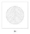
【選択図】図4
Description
Claims (6)
- パッケージ基板とパッケージ基板に設けられるチップユニットを含み、前記チップユニットは少なくとも一つのベアチップユニットとベアチップユニットの表面に一層の第1の蛍光層を被覆してなる少なくとも一つのパッケージ化されたチップユニットに分けられ、前記ベアチップユニットとパッケージ化されたチップユニットの色温度が異なり、更に上記ベアチップユニットとパッケージ化されたチップユニットを被覆する第2の蛍光層が設けられることを特徴とする効率的なLEDインテリジェント光源。
- 前記パッケージ化されたチップユニットの色温度が一つであり、前記ベアチップユニットとパッケージ化されたチップユニットが均一に交錯して分布することを特徴とする請求項1に記載の効率的なLEDインテリジェント光源。
- 前記パッケージ化されたチップユニットの色温度は少なくとも二つであり、且つ異なる色温度のパッケージ化されたチップユニットとベアチップユニットが均一に交錯して分布することを特徴とする請求項1に記載の効率的なLEDインテリジェント光源。
- 前記ベアチップユニットは少なくとも一つのチップからなることを特徴とする請求項1から3のいずれか一項に記載の効率的なLEDインテリジェント光源。
- 前記第1の蛍光層は遷移蛍光パウダーであることを特徴とする請求項1から3のいずれか一項に記載の効率的なLEDインテリジェント光源。
- 前記第2の蛍光層はパッケージングのための蛍光接着剤であることを特徴とする請求項1から3のいずれか一項に記載の効率的なLEDインテリジェント光源。
Applications Claiming Priority (3)
| Application Number | Priority Date | Filing Date | Title |
|---|---|---|---|
| CN201511008300.5 | 2015-12-25 | ||
| CN201511008300.5A CN105423149A (zh) | 2015-12-25 | 2015-12-25 | 一种高效led智能光源 |
| PCT/CN2016/108993 WO2017107776A1 (zh) | 2015-12-25 | 2016-12-08 | 一种高效led智能光源 |
Publications (1)
| Publication Number | Publication Date |
|---|---|
| JP2018535552A true JP2018535552A (ja) | 2018-11-29 |
Family
ID=55501563
Family Applications (1)
| Application Number | Title | Priority Date | Filing Date |
|---|---|---|---|
| JP2018522619A Pending JP2018535552A (ja) | 2015-12-25 | 2016-12-08 | 効率的なledインテリジェント光源 |
Country Status (5)
| Country | Link |
|---|---|
| US (1) | US20180315902A1 (ja) |
| EP (1) | EP3358241A4 (ja) |
| JP (1) | JP2018535552A (ja) |
| CN (1) | CN105423149A (ja) |
| WO (1) | WO2017107776A1 (ja) |
Cited By (1)
| Publication number | Priority date | Publication date | Assignee | Title |
|---|---|---|---|---|
| US11244931B2 (en) | 2018-10-04 | 2022-02-08 | Nichia Corporation | Light emitting device with enhanced color mixing quality |
Families Citing this family (11)
| Publication number | Priority date | Publication date | Assignee | Title |
|---|---|---|---|---|
| CN105423149A (zh) * | 2015-12-25 | 2016-03-23 | 广州市添鑫光电有限公司 | 一种高效led智能光源 |
| CN105977245A (zh) * | 2016-07-18 | 2016-09-28 | 中山市立体光电科技有限公司 | 一种可调色温的cob封装结构及其封装方法 |
| CN105977244A (zh) * | 2016-07-18 | 2016-09-28 | 中山市立体光电科技有限公司 | 一种可调色温的csp封装器件及其封装方法 |
| CN106409820A (zh) * | 2016-10-24 | 2017-02-15 | 中山市立体光电科技有限公司 | 一种可调色温的led灯珠及其封装方法 |
| CN106678730A (zh) * | 2017-03-03 | 2017-05-17 | 四川鋈新能源科技有限公司 | 色温可调的led灯丝及led灯泡 |
| CN107579060A (zh) * | 2017-09-13 | 2018-01-12 | 深圳市未林森科技有限公司 | 一种集成双色led灯及其制造方法 |
| CN108561764B (zh) * | 2018-03-21 | 2019-11-22 | 厦门市三安光电科技有限公司 | Led灯丝结构及基于其的led照明灯 |
| CN109742067A (zh) * | 2018-12-10 | 2019-05-10 | 广东晶科电子股份有限公司 | 一种发光二极管及其制作方法 |
| US11209129B2 (en) * | 2019-01-29 | 2021-12-28 | Xiamen Eco Lighting Co. Ltd. | Light apparatus |
| US11398458B2 (en) | 2019-12-13 | 2022-07-26 | Lumileds Llc | Multi-color phosphor converted LED package with single cavity |
| WO2021119465A1 (en) * | 2019-12-13 | 2021-06-17 | Lumileds Llc | Leds and multi-color phosphors |
Citations (8)
| Publication number | Priority date | Publication date | Assignee | Title |
|---|---|---|---|---|
| WO2005086239A1 (ja) * | 2004-03-05 | 2005-09-15 | Konica Minolta Holdings, Inc. | 白色発光ダイオード(led)及び白色ledの製造方法 |
| JP2011529621A (ja) * | 2008-07-29 | 2011-12-08 | ソウル セミコンダクター カンパニー リミテッド | ウォームホワイト発光装置及びそれを備えるバックライトモジュール |
| JP2013120812A (ja) * | 2011-12-07 | 2013-06-17 | Mitsubishi Electric Corp | 発光装置 |
| JP2014049504A (ja) * | 2012-08-29 | 2014-03-17 | Sharp Corp | 発光装置及びその製造方法 |
| WO2015015363A1 (en) * | 2013-08-01 | 2015-02-05 | Koninklijke Philips N.V. | Light emitting arrangement with adapted output spectrum |
| US20150034980A1 (en) * | 2013-08-05 | 2015-02-05 | Osram Gmbh | Phosphor led |
| JP2015106660A (ja) * | 2013-11-29 | 2015-06-08 | シチズン電子株式会社 | 発光装置 |
| US20150228629A1 (en) * | 2014-02-10 | 2015-08-13 | Edison Opto Crporation | Dimmable light-emitted diode (led) packaging structure |
Family Cites Families (11)
| Publication number | Priority date | Publication date | Assignee | Title |
|---|---|---|---|---|
| KR20090001104A (ko) * | 2007-06-29 | 2009-01-08 | 서울반도체 주식회사 | 다양한 색온도를 갖는 발광 장치 |
| CN101958286A (zh) * | 2010-08-19 | 2011-01-26 | 深圳市佳比泰电子科技有限公司 | 一种封装可变色温的白光led的方法 |
| CN102956625A (zh) * | 2011-08-18 | 2013-03-06 | 鸿富锦精密工业(深圳)有限公司 | 发光装置 |
| CN202209554U (zh) * | 2011-08-25 | 2012-05-02 | 天津雍光半导体照明有限公司 | 集成式可调色温白光led |
| CN102569282A (zh) * | 2012-01-18 | 2012-07-11 | 浙江英特来光电科技有限公司 | 一种可调光调色led结构 |
| CN202598261U (zh) * | 2012-06-07 | 2012-12-12 | 深圳市红绿蓝光电科技有限公司 | 一种高亮度高显色指数的暖白光led灯及led模组 |
| EP2953174B1 (en) * | 2013-01-31 | 2020-07-01 | Kabushiki Kaisha Toshiba | Light emitting device and led light bulb |
| CN203240331U (zh) * | 2013-03-27 | 2013-10-16 | 珠海市集利发展有限公司 | 基于阵列分布的可调光led集成光源 |
| CN203979913U (zh) * | 2014-01-13 | 2014-12-03 | 重庆信德电子有限公司 | 色温、亮度可调的led白光组件 |
| CN105423149A (zh) * | 2015-12-25 | 2016-03-23 | 广州市添鑫光电有限公司 | 一种高效led智能光源 |
| CN205372111U (zh) * | 2015-12-25 | 2016-07-06 | 广州市添鑫光电有限公司 | 一种高效led智能光源 |
-
2015
- 2015-12-25 CN CN201511008300.5A patent/CN105423149A/zh active Pending
-
2016
- 2016-12-08 US US15/771,089 patent/US20180315902A1/en not_active Abandoned
- 2016-12-08 JP JP2018522619A patent/JP2018535552A/ja active Pending
- 2016-12-08 EP EP16877587.2A patent/EP3358241A4/en not_active Withdrawn
- 2016-12-08 WO PCT/CN2016/108993 patent/WO2017107776A1/zh active Application Filing
Patent Citations (8)
| Publication number | Priority date | Publication date | Assignee | Title |
|---|---|---|---|---|
| WO2005086239A1 (ja) * | 2004-03-05 | 2005-09-15 | Konica Minolta Holdings, Inc. | 白色発光ダイオード(led)及び白色ledの製造方法 |
| JP2011529621A (ja) * | 2008-07-29 | 2011-12-08 | ソウル セミコンダクター カンパニー リミテッド | ウォームホワイト発光装置及びそれを備えるバックライトモジュール |
| JP2013120812A (ja) * | 2011-12-07 | 2013-06-17 | Mitsubishi Electric Corp | 発光装置 |
| JP2014049504A (ja) * | 2012-08-29 | 2014-03-17 | Sharp Corp | 発光装置及びその製造方法 |
| WO2015015363A1 (en) * | 2013-08-01 | 2015-02-05 | Koninklijke Philips N.V. | Light emitting arrangement with adapted output spectrum |
| US20150034980A1 (en) * | 2013-08-05 | 2015-02-05 | Osram Gmbh | Phosphor led |
| JP2015106660A (ja) * | 2013-11-29 | 2015-06-08 | シチズン電子株式会社 | 発光装置 |
| US20150228629A1 (en) * | 2014-02-10 | 2015-08-13 | Edison Opto Crporation | Dimmable light-emitted diode (led) packaging structure |
Cited By (1)
| Publication number | Priority date | Publication date | Assignee | Title |
|---|---|---|---|---|
| US11244931B2 (en) | 2018-10-04 | 2022-02-08 | Nichia Corporation | Light emitting device with enhanced color mixing quality |
Also Published As
| Publication number | Publication date |
|---|---|
| EP3358241A1 (en) | 2018-08-08 |
| US20180315902A1 (en) | 2018-11-01 |
| WO2017107776A1 (zh) | 2017-06-29 |
| EP3358241A4 (en) | 2018-08-15 |
| CN105423149A (zh) | 2016-03-23 |
Similar Documents
| Publication | Publication Date | Title |
|---|---|---|
| JP2018535552A (ja) | 効率的なledインテリジェント光源 | |
| US9746142B2 (en) | Scattered-photon extraction-based fixtures | |
| US9316368B2 (en) | LED luminaire including a thin phosphor layer applied to a remote reflector | |
| US9897276B2 (en) | Reduced phosphor lighting devices | |
| US20140369036A1 (en) | Led light and filament thereof | |
| CN203642078U (zh) | 光源及具备该光源的照明器具 | |
| KR20110026490A (ko) | 광혼합재를 포함하는 고상 조명 디바이스 | |
| JP2017532793A (ja) | Led封止に使用する基板、3次元led封止体、3次元led封止体を有する電球及びこれらの製造方法 | |
| JP2007059272A (ja) | 照明装置及び照明方法 | |
| US20140106639A1 (en) | Automated color tuning of an led based illumination device | |
| JP2017098522A (ja) | Led発光装置の製造方法及びその発光装置 | |
| TW201250170A (en) | Light emitting diode light bulbs and light emitting diode assemblies thereof | |
| WO2018028439A1 (zh) | 光源模组及带有光源模组的灯具 | |
| CN105972462A (zh) | 一种色温可调的led球泡灯 | |
| CN102679194B (zh) | Led灯具 | |
| CN102969308B (zh) | 一种led灯结构及其封装方法 | |
| CN205372111U (zh) | 一种高效led智能光源 | |
| CN204254320U (zh) | 发光二极管封装结构及发光器件 | |
| US20150131260A1 (en) | Light-emitting device comprising a hollow retro-reflector | |
| JP6256528B2 (ja) | 照明器具 | |
| US20130169144A1 (en) | Led package structure capable of adjusting the spatial color uniformity and the light distribution curve | |
| CN203868787U (zh) | 一种远程荧光粉led灯 | |
| JP2014135322A (ja) | 発光装置及び照明器具 | |
| US20170279016A1 (en) | Luminance pattern shaping using a back-emitting led and a reflective substrate | |
| JP6460581B2 (ja) | 照明器具 |
Legal Events
| Date | Code | Title | Description |
|---|---|---|---|
| A521 | Request for written amendment filed |
Free format text: JAPANESE INTERMEDIATE CODE: A821 Effective date: 20180510 |
|
| A621 | Written request for application examination |
Free format text: JAPANESE INTERMEDIATE CODE: A621 Effective date: 20180510 |
|
| RD01 | Notification of change of attorney |
Free format text: JAPANESE INTERMEDIATE CODE: A7426 Effective date: 20180510 |
|
| A977 | Report on retrieval |
Free format text: JAPANESE INTERMEDIATE CODE: A971007 Effective date: 20190320 |
|
| A131 | Notification of reasons for refusal |
Free format text: JAPANESE INTERMEDIATE CODE: A131 Effective date: 20190402 |
|
| A601 | Written request for extension of time |
Free format text: JAPANESE INTERMEDIATE CODE: A601 Effective date: 20190606 |
|
| A02 | Decision of refusal |
Free format text: JAPANESE INTERMEDIATE CODE: A02 Effective date: 20191029 |