JP2018117070A - 半導体装置及びその製造方法 - Google Patents
半導体装置及びその製造方法 Download PDFInfo
- Publication number
- JP2018117070A JP2018117070A JP2017007552A JP2017007552A JP2018117070A JP 2018117070 A JP2018117070 A JP 2018117070A JP 2017007552 A JP2017007552 A JP 2017007552A JP 2017007552 A JP2017007552 A JP 2017007552A JP 2018117070 A JP2018117070 A JP 2018117070A
- Authority
- JP
- Japan
- Prior art keywords
- trench
- insulating film
- substrate
- region
- height
- Prior art date
- Legal status (The legal status is an assumption and is not a legal conclusion. Google has not performed a legal analysis and makes no representation as to the accuracy of the status listed.)
- Pending
Links
- 239000004065 semiconductor Substances 0.000 title claims abstract description 71
- 238000004519 manufacturing process Methods 0.000 title claims abstract description 25
- 239000000758 substrate Substances 0.000 claims abstract description 73
- 239000012535 impurity Substances 0.000 claims description 14
- 238000000034 method Methods 0.000 claims description 9
- 238000005530 etching Methods 0.000 claims description 8
- 238000005468 ion implantation Methods 0.000 claims description 4
- 238000009413 insulation Methods 0.000 abstract 3
- 239000010410 layer Substances 0.000 description 34
- 239000011229 interlayer Substances 0.000 description 13
- 229920002120 photoresistant polymer Polymers 0.000 description 4
- 238000005229 chemical vapour deposition Methods 0.000 description 2
- 230000000694 effects Effects 0.000 description 2
- 238000000206 photolithography Methods 0.000 description 2
- 230000015572 biosynthetic process Effects 0.000 description 1
- 210000000746 body region Anatomy 0.000 description 1
- 239000004020 conductor Substances 0.000 description 1
- 230000003247 decreasing effect Effects 0.000 description 1
- 239000007772 electrode material Substances 0.000 description 1
- 230000001590 oxidative effect Effects 0.000 description 1
- 229910021420 polycrystalline silicon Inorganic materials 0.000 description 1
- 229920005591 polysilicon Polymers 0.000 description 1
Images


Classifications
-
- H—ELECTRICITY
- H01—ELECTRIC ELEMENTS
- H01L—SEMICONDUCTOR DEVICES NOT COVERED BY CLASS H10
- H01L29/00—Semiconductor devices adapted for rectifying, amplifying, oscillating or switching, or capacitors or resistors with at least one potential-jump barrier or surface barrier, e.g. PN junction depletion layer or carrier concentration layer; Details of semiconductor bodies or of electrodes thereof ; Multistep manufacturing processes therefor
- H01L29/40—Electrodes ; Multistep manufacturing processes therefor
- H01L29/41—Electrodes ; Multistep manufacturing processes therefor characterised by their shape, relative sizes or dispositions
- H01L29/417—Electrodes ; Multistep manufacturing processes therefor characterised by their shape, relative sizes or dispositions carrying the current to be rectified, amplified or switched
- H01L29/41725—Source or drain electrodes for field effect devices
- H01L29/41741—Source or drain electrodes for field effect devices for vertical or pseudo-vertical devices
-
- H—ELECTRICITY
- H01—ELECTRIC ELEMENTS
- H01L—SEMICONDUCTOR DEVICES NOT COVERED BY CLASS H10
- H01L29/00—Semiconductor devices adapted for rectifying, amplifying, oscillating or switching, or capacitors or resistors with at least one potential-jump barrier or surface barrier, e.g. PN junction depletion layer or carrier concentration layer; Details of semiconductor bodies or of electrodes thereof ; Multistep manufacturing processes therefor
- H01L29/66—Types of semiconductor device ; Multistep manufacturing processes therefor
- H01L29/68—Types of semiconductor device ; Multistep manufacturing processes therefor controllable by only the electric current supplied, or only the electric potential applied, to an electrode which does not carry the current to be rectified, amplified or switched
- H01L29/70—Bipolar devices
- H01L29/72—Transistor-type devices, i.e. able to continuously respond to applied control signals
- H01L29/73—Bipolar junction transistors
- H01L29/732—Vertical transistors
-
- H—ELECTRICITY
- H01—ELECTRIC ELEMENTS
- H01L—SEMICONDUCTOR DEVICES NOT COVERED BY CLASS H10
- H01L29/00—Semiconductor devices adapted for rectifying, amplifying, oscillating or switching, or capacitors or resistors with at least one potential-jump barrier or surface barrier, e.g. PN junction depletion layer or carrier concentration layer; Details of semiconductor bodies or of electrodes thereof ; Multistep manufacturing processes therefor
- H01L29/66—Types of semiconductor device ; Multistep manufacturing processes therefor
- H01L29/68—Types of semiconductor device ; Multistep manufacturing processes therefor controllable by only the electric current supplied, or only the electric potential applied, to an electrode which does not carry the current to be rectified, amplified or switched
- H01L29/76—Unipolar devices, e.g. field effect transistors
- H01L29/772—Field effect transistors
- H01L29/78—Field effect transistors with field effect produced by an insulated gate
- H01L29/7801—DMOS transistors, i.e. MISFETs with a channel accommodating body or base region adjoining a drain drift region
- H01L29/7802—Vertical DMOS transistors, i.e. VDMOS transistors
-
- H—ELECTRICITY
- H01—ELECTRIC ELEMENTS
- H01L—SEMICONDUCTOR DEVICES NOT COVERED BY CLASS H10
- H01L21/00—Processes or apparatus adapted for the manufacture or treatment of semiconductor or solid state devices or of parts thereof
- H01L21/70—Manufacture or treatment of devices consisting of a plurality of solid state components formed in or on a common substrate or of parts thereof; Manufacture of integrated circuit devices or of parts thereof
- H01L21/71—Manufacture of specific parts of devices defined in group H01L21/70
- H01L21/768—Applying interconnections to be used for carrying current between separate components within a device comprising conductors and dielectrics
- H01L21/76838—Applying interconnections to be used for carrying current between separate components within a device comprising conductors and dielectrics characterised by the formation and the after-treatment of the conductors
- H01L21/76841—Barrier, adhesion or liner layers
- H01L21/76853—Barrier, adhesion or liner layers characterized by particular after-treatment steps
- H01L21/76855—After-treatment introducing at least one additional element into the layer
- H01L21/76859—After-treatment introducing at least one additional element into the layer by ion implantation
-
- H—ELECTRICITY
- H01—ELECTRIC ELEMENTS
- H01L—SEMICONDUCTOR DEVICES NOT COVERED BY CLASS H10
- H01L29/00—Semiconductor devices adapted for rectifying, amplifying, oscillating or switching, or capacitors or resistors with at least one potential-jump barrier or surface barrier, e.g. PN junction depletion layer or carrier concentration layer; Details of semiconductor bodies or of electrodes thereof ; Multistep manufacturing processes therefor
- H01L29/02—Semiconductor bodies ; Multistep manufacturing processes therefor
- H01L29/06—Semiconductor bodies ; Multistep manufacturing processes therefor characterised by their shape; characterised by the shapes, relative sizes, or dispositions of the semiconductor regions ; characterised by the concentration or distribution of impurities within semiconductor regions
- H01L29/0603—Semiconductor bodies ; Multistep manufacturing processes therefor characterised by their shape; characterised by the shapes, relative sizes, or dispositions of the semiconductor regions ; characterised by the concentration or distribution of impurities within semiconductor regions characterised by particular constructional design considerations, e.g. for preventing surface leakage, for controlling electric field concentration or for internal isolations regions
-
- H—ELECTRICITY
- H01—ELECTRIC ELEMENTS
- H01L—SEMICONDUCTOR DEVICES NOT COVERED BY CLASS H10
- H01L29/00—Semiconductor devices adapted for rectifying, amplifying, oscillating or switching, or capacitors or resistors with at least one potential-jump barrier or surface barrier, e.g. PN junction depletion layer or carrier concentration layer; Details of semiconductor bodies or of electrodes thereof ; Multistep manufacturing processes therefor
- H01L29/02—Semiconductor bodies ; Multistep manufacturing processes therefor
- H01L29/06—Semiconductor bodies ; Multistep manufacturing processes therefor characterised by their shape; characterised by the shapes, relative sizes, or dispositions of the semiconductor regions ; characterised by the concentration or distribution of impurities within semiconductor regions
- H01L29/0684—Semiconductor bodies ; Multistep manufacturing processes therefor characterised by their shape; characterised by the shapes, relative sizes, or dispositions of the semiconductor regions ; characterised by the concentration or distribution of impurities within semiconductor regions characterised by the shape, relative sizes or dispositions of the semiconductor regions or junctions between the regions
-
- H—ELECTRICITY
- H01—ELECTRIC ELEMENTS
- H01L—SEMICONDUCTOR DEVICES NOT COVERED BY CLASS H10
- H01L29/00—Semiconductor devices adapted for rectifying, amplifying, oscillating or switching, or capacitors or resistors with at least one potential-jump barrier or surface barrier, e.g. PN junction depletion layer or carrier concentration layer; Details of semiconductor bodies or of electrodes thereof ; Multistep manufacturing processes therefor
- H01L29/02—Semiconductor bodies ; Multistep manufacturing processes therefor
- H01L29/06—Semiconductor bodies ; Multistep manufacturing processes therefor characterised by their shape; characterised by the shapes, relative sizes, or dispositions of the semiconductor regions ; characterised by the concentration or distribution of impurities within semiconductor regions
- H01L29/10—Semiconductor bodies ; Multistep manufacturing processes therefor characterised by their shape; characterised by the shapes, relative sizes, or dispositions of the semiconductor regions ; characterised by the concentration or distribution of impurities within semiconductor regions with semiconductor regions connected to an electrode not carrying current to be rectified, amplified or switched and such electrode being part of a semiconductor device which comprises three or more electrodes
- H01L29/1095—Body region, i.e. base region, of DMOS transistors or IGBTs
-
- H—ELECTRICITY
- H01—ELECTRIC ELEMENTS
- H01L—SEMICONDUCTOR DEVICES NOT COVERED BY CLASS H10
- H01L29/00—Semiconductor devices adapted for rectifying, amplifying, oscillating or switching, or capacitors or resistors with at least one potential-jump barrier or surface barrier, e.g. PN junction depletion layer or carrier concentration layer; Details of semiconductor bodies or of electrodes thereof ; Multistep manufacturing processes therefor
- H01L29/40—Electrodes ; Multistep manufacturing processes therefor
- H01L29/41—Electrodes ; Multistep manufacturing processes therefor characterised by their shape, relative sizes or dispositions
- H01L29/417—Electrodes ; Multistep manufacturing processes therefor characterised by their shape, relative sizes or dispositions carrying the current to be rectified, amplified or switched
- H01L29/41725—Source or drain electrodes for field effect devices
- H01L29/41766—Source or drain electrodes for field effect devices with at least part of the source or drain electrode having contact below the semiconductor surface, e.g. the source or drain electrode formed at least partially in a groove or with inclusions of conductor inside the semiconductor
-
- H—ELECTRICITY
- H01—ELECTRIC ELEMENTS
- H01L—SEMICONDUCTOR DEVICES NOT COVERED BY CLASS H10
- H01L29/00—Semiconductor devices adapted for rectifying, amplifying, oscillating or switching, or capacitors or resistors with at least one potential-jump barrier or surface barrier, e.g. PN junction depletion layer or carrier concentration layer; Details of semiconductor bodies or of electrodes thereof ; Multistep manufacturing processes therefor
- H01L29/40—Electrodes ; Multistep manufacturing processes therefor
- H01L29/41—Electrodes ; Multistep manufacturing processes therefor characterised by their shape, relative sizes or dispositions
- H01L29/423—Electrodes ; Multistep manufacturing processes therefor characterised by their shape, relative sizes or dispositions not carrying the current to be rectified, amplified or switched
- H01L29/42312—Gate electrodes for field effect devices
- H01L29/42316—Gate electrodes for field effect devices for field-effect transistors
- H01L29/4232—Gate electrodes for field effect devices for field-effect transistors with insulated gate
- H01L29/42356—Disposition, e.g. buried gate electrode
- H01L29/4236—Disposition, e.g. buried gate electrode within a trench, e.g. trench gate electrode, groove gate electrode
-
- H—ELECTRICITY
- H01—ELECTRIC ELEMENTS
- H01L—SEMICONDUCTOR DEVICES NOT COVERED BY CLASS H10
- H01L29/00—Semiconductor devices adapted for rectifying, amplifying, oscillating or switching, or capacitors or resistors with at least one potential-jump barrier or surface barrier, e.g. PN junction depletion layer or carrier concentration layer; Details of semiconductor bodies or of electrodes thereof ; Multistep manufacturing processes therefor
- H01L29/66—Types of semiconductor device ; Multistep manufacturing processes therefor
- H01L29/66007—Multistep manufacturing processes
- H01L29/66075—Multistep manufacturing processes of devices having semiconductor bodies comprising group 14 or group 13/15 materials
- H01L29/66227—Multistep manufacturing processes of devices having semiconductor bodies comprising group 14 or group 13/15 materials the devices being controllable only by the electric current supplied or the electric potential applied, to an electrode which does not carry the current to be rectified, amplified or switched, e.g. three-terminal devices
- H01L29/66409—Unipolar field-effect transistors
- H01L29/66477—Unipolar field-effect transistors with an insulated gate, i.e. MISFET
- H01L29/66666—Vertical transistors
-
- H—ELECTRICITY
- H01—ELECTRIC ELEMENTS
- H01L—SEMICONDUCTOR DEVICES NOT COVERED BY CLASS H10
- H01L29/00—Semiconductor devices adapted for rectifying, amplifying, oscillating or switching, or capacitors or resistors with at least one potential-jump barrier or surface barrier, e.g. PN junction depletion layer or carrier concentration layer; Details of semiconductor bodies or of electrodes thereof ; Multistep manufacturing processes therefor
- H01L29/66—Types of semiconductor device ; Multistep manufacturing processes therefor
- H01L29/66007—Multistep manufacturing processes
- H01L29/66075—Multistep manufacturing processes of devices having semiconductor bodies comprising group 14 or group 13/15 materials
- H01L29/66227—Multistep manufacturing processes of devices having semiconductor bodies comprising group 14 or group 13/15 materials the devices being controllable only by the electric current supplied or the electric potential applied, to an electrode which does not carry the current to be rectified, amplified or switched, e.g. three-terminal devices
- H01L29/66409—Unipolar field-effect transistors
- H01L29/66477—Unipolar field-effect transistors with an insulated gate, i.e. MISFET
- H01L29/66674—DMOS transistors, i.e. MISFETs with a channel accommodating body or base region adjoining a drain drift region
- H01L29/66712—Vertical DMOS transistors, i.e. VDMOS transistors
- H01L29/66727—Vertical DMOS transistors, i.e. VDMOS transistors with a step of recessing the source electrode
-
- H—ELECTRICITY
- H01—ELECTRIC ELEMENTS
- H01L—SEMICONDUCTOR DEVICES NOT COVERED BY CLASS H10
- H01L29/00—Semiconductor devices adapted for rectifying, amplifying, oscillating or switching, or capacitors or resistors with at least one potential-jump barrier or surface barrier, e.g. PN junction depletion layer or carrier concentration layer; Details of semiconductor bodies or of electrodes thereof ; Multistep manufacturing processes therefor
- H01L29/66—Types of semiconductor device ; Multistep manufacturing processes therefor
- H01L29/66007—Multistep manufacturing processes
- H01L29/66075—Multistep manufacturing processes of devices having semiconductor bodies comprising group 14 or group 13/15 materials
- H01L29/66227—Multistep manufacturing processes of devices having semiconductor bodies comprising group 14 or group 13/15 materials the devices being controllable only by the electric current supplied or the electric potential applied, to an electrode which does not carry the current to be rectified, amplified or switched, e.g. three-terminal devices
- H01L29/66409—Unipolar field-effect transistors
- H01L29/66477—Unipolar field-effect transistors with an insulated gate, i.e. MISFET
- H01L29/66674—DMOS transistors, i.e. MISFETs with a channel accommodating body or base region adjoining a drain drift region
- H01L29/66712—Vertical DMOS transistors, i.e. VDMOS transistors
- H01L29/66734—Vertical DMOS transistors, i.e. VDMOS transistors with a step of recessing the gate electrode, e.g. to form a trench gate electrode
-
- H—ELECTRICITY
- H01—ELECTRIC ELEMENTS
- H01L—SEMICONDUCTOR DEVICES NOT COVERED BY CLASS H10
- H01L29/00—Semiconductor devices adapted for rectifying, amplifying, oscillating or switching, or capacitors or resistors with at least one potential-jump barrier or surface barrier, e.g. PN junction depletion layer or carrier concentration layer; Details of semiconductor bodies or of electrodes thereof ; Multistep manufacturing processes therefor
- H01L29/66—Types of semiconductor device ; Multistep manufacturing processes therefor
- H01L29/68—Types of semiconductor device ; Multistep manufacturing processes therefor controllable by only the electric current supplied, or only the electric potential applied, to an electrode which does not carry the current to be rectified, amplified or switched
- H01L29/76—Unipolar devices, e.g. field effect transistors
- H01L29/772—Field effect transistors
- H01L29/78—Field effect transistors with field effect produced by an insulated gate
- H01L29/7801—DMOS transistors, i.e. MISFETs with a channel accommodating body or base region adjoining a drain drift region
- H01L29/7802—Vertical DMOS transistors, i.e. VDMOS transistors
- H01L29/7813—Vertical DMOS transistors, i.e. VDMOS transistors with trench gate electrode, e.g. UMOS transistors
-
- H—ELECTRICITY
- H01—ELECTRIC ELEMENTS
- H01L—SEMICONDUCTOR DEVICES NOT COVERED BY CLASS H10
- H01L21/00—Processes or apparatus adapted for the manufacture or treatment of semiconductor or solid state devices or of parts thereof
- H01L21/02—Manufacture or treatment of semiconductor devices or of parts thereof
- H01L21/04—Manufacture or treatment of semiconductor devices or of parts thereof the devices having at least one potential-jump barrier or surface barrier, e.g. PN junction, depletion layer or carrier concentration layer
- H01L21/18—Manufacture or treatment of semiconductor devices or of parts thereof the devices having at least one potential-jump barrier or surface barrier, e.g. PN junction, depletion layer or carrier concentration layer the devices having semiconductor bodies comprising elements of Group IV of the Periodic System or AIIIBV compounds with or without impurities, e.g. doping materials
- H01L21/26—Bombardment with radiation
- H01L21/263—Bombardment with radiation with high-energy radiation
- H01L21/265—Bombardment with radiation with high-energy radiation producing ion implantation
- H01L21/26586—Bombardment with radiation with high-energy radiation producing ion implantation characterised by the angle between the ion beam and the crystal planes or the main crystal surface
-
- H—ELECTRICITY
- H01—ELECTRIC ELEMENTS
- H01L—SEMICONDUCTOR DEVICES NOT COVERED BY CLASS H10
- H01L29/00—Semiconductor devices adapted for rectifying, amplifying, oscillating or switching, or capacitors or resistors with at least one potential-jump barrier or surface barrier, e.g. PN junction depletion layer or carrier concentration layer; Details of semiconductor bodies or of electrodes thereof ; Multistep manufacturing processes therefor
- H01L29/02—Semiconductor bodies ; Multistep manufacturing processes therefor
- H01L29/06—Semiconductor bodies ; Multistep manufacturing processes therefor characterised by their shape; characterised by the shapes, relative sizes, or dispositions of the semiconductor regions ; characterised by the concentration or distribution of impurities within semiconductor regions
- H01L29/0684—Semiconductor bodies ; Multistep manufacturing processes therefor characterised by their shape; characterised by the shapes, relative sizes, or dispositions of the semiconductor regions ; characterised by the concentration or distribution of impurities within semiconductor regions characterised by the shape, relative sizes or dispositions of the semiconductor regions or junctions between the regions
- H01L29/0692—Surface layout
- H01L29/0696—Surface layout of cellular field-effect devices, e.g. multicellular DMOS transistors or IGBTs
-
- H—ELECTRICITY
- H01—ELECTRIC ELEMENTS
- H01L—SEMICONDUCTOR DEVICES NOT COVERED BY CLASS H10
- H01L29/00—Semiconductor devices adapted for rectifying, amplifying, oscillating or switching, or capacitors or resistors with at least one potential-jump barrier or surface barrier, e.g. PN junction depletion layer or carrier concentration layer; Details of semiconductor bodies or of electrodes thereof ; Multistep manufacturing processes therefor
- H01L29/02—Semiconductor bodies ; Multistep manufacturing processes therefor
- H01L29/06—Semiconductor bodies ; Multistep manufacturing processes therefor characterised by their shape; characterised by the shapes, relative sizes, or dispositions of the semiconductor regions ; characterised by the concentration or distribution of impurities within semiconductor regions
- H01L29/08—Semiconductor bodies ; Multistep manufacturing processes therefor characterised by their shape; characterised by the shapes, relative sizes, or dispositions of the semiconductor regions ; characterised by the concentration or distribution of impurities within semiconductor regions with semiconductor regions connected to an electrode carrying current to be rectified, amplified or switched and such electrode being part of a semiconductor device which comprises three or more electrodes
- H01L29/0843—Source or drain regions of field-effect devices
- H01L29/0847—Source or drain regions of field-effect devices of field-effect transistors with insulated gate
- H01L29/0852—Source or drain regions of field-effect devices of field-effect transistors with insulated gate of DMOS transistors
- H01L29/0856—Source regions
- H01L29/0865—Disposition
Abstract
【解決手段】基板と、基板の裏面側に設けられたドレイン領域と、ドレイン領域から基板表面間に設けられたベース層と、基板表面からドレイン領域に達するトレンチと、トレンチの底面から第一の高さまでのトレンチ内側を覆うゲート絶縁膜と、ゲート絶縁膜を介して同じ高さまで埋め込まれたゲート電極と、第一の高さより高い第二の高さまで埋め込まれた絶縁膜と、トレンチ内の残りの部分に埋め込まれたソース電極と、基板の表面から第二の高さよりも浅く設けられた、片側面がソース電極に接するベースコンタクト領域と、上面がベースコンタクト領域の底面の一部に接し、片側面がトレンチの側面に接するとともに一部がソース電極に接するソース領域と、基板の裏面上のドレイン電極とを備える。
【選択図】図1
Description
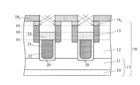
図1は、本発明の第一の実施形態の縦型MOSFETを有する半導体装置100を説明するための断面図である。
図3に示すように、N型不純物が高濃度にドープされた高濃度半導体基板10の上に、エピタキシャル成長により、N型不純物がドープされたエピタキシャル層15を形成する。これにより、基板16が形成される。
続いて、トレンチ20をゲート電極材料で上部まで埋めた後に、図8に示すように、第一の高さH1までエッチバックすることで、ゲート電極22を形成する。
また、トレンチ20を除く基板16の表面上に、絶縁膜242が設けられている。
これら平面構造についても、第一の実施形態の半導体装置100とほぼ同様であるため、異なる点を中心に説明する。
第一の実施形態と同様にして図3から図5までの工程を経た後、図14のように絶縁膜24を絶縁膜242として残存させたままトレンチの底面及び側面にゲート絶縁膜21を形成する。
続いて、図16のように、トレンチ20内を層間絶縁膜23で埋め、第一の高さH1より高い第二の高さまでエッチバックすることで層間絶縁膜23を形成する。
例えば、上記実施形態で説明した半導体装置の構成において、P型とN型の構成要素の導電型を全て逆にしても良い。
また、図2(b)及び図13(b)には、本発明の実施形態による半導体装置の平面構造として、トレンチ20によって囲まれた各領域が四角形である例を示したが、この領域は四角形に限らず、四角形の角を落とした八角形や円形等であっても構わない。
11 半導体層
12 ベース層
13 ソース領域
14、142 ベースコンタクト領域
15 エピタキシャル層
16 基板
17 ドレイン領域
20 トレンチ
21 ゲート酸化膜
22 ゲート電極
23 層間絶縁膜
24、242 絶縁膜
32 ドレイン電極
33 ソース電極
40 フォトレジスト
H1 第一の高さ
H2 第二の高さ
H3 第三の高さ
Claims (10)
- 基板と、
前記基板の裏面から所定の厚さを有して前記基板に設けられた第一導電型のドレイン領域と、
前記基板の表面から前記ドレイン領域の上面に達するトレンチと、
前記トレンチに隣接して前記ドレイン領域上に設けられた第二導電型のベース層と、
前記トレンチの内側の底面及び側面を覆い、上端部が前記トレンチの底面から第一の高さに位置するゲート絶縁膜と、
前記トレンチ内に前記ゲート絶縁膜を介して前記第一の高さまで埋め込まれたゲート電極と、
前記トレンチ内の前記ゲート絶縁膜及び前記ゲート電極上に前記第一の高さよりも高い第二の高さまで埋め込まれた第一の絶縁膜と、
前記トレンチ内の前記第一の絶縁膜上の残りの部分に埋め込まれたソース電極と、
前記基板の表面から、前記第二の高さより高く前記トレンチの上部よりも低い第三の高さまでの深さを有し、一方の側面が前記ソース電極に接して設けられた前記ベース層よりも高濃度の第二導電型のベースコンタクト領域と、
上面が前記ベースコンタクト領域の底面の一部に接し、一方の側面が前記トレンチの外側面に接するとともに該一方の側面の少なくとも一部が前記ソース電極に接し、底面から前記ドレイン領域までの前記トレンチの外側面に沿った前記ベース層がチャネル領域となるように設けられた第二導電型のソース領域と、
前記基板の裏面上に前記ドレイン領域に接して設けられたドレイン電極とを備えることを特徴とする半導体装置。 - 前記ベースコンタクト領域は、底面の一部が前記ベース層に接していることを特徴とする請求項1に記載の半導体装置。
- 前記ベースコンタクト領域は、他方の側面が前記ベース層に接していることを特徴とする請求項1に記載の半導体装置。
- 前記ベースコンタクト領域上に設けられ、前記トレンチの上部に繋がる開口を有する第二の絶縁膜をさらに備え、前記ソース電極は前記開口内にも埋め込まれていることを特徴とする請求項1乃至3のいずれか一項に記載の半導体装置。
- 前記トレンチは、所定の方向に延在していることを特徴とする請求項1乃至4のいずれか一項に記載の半導体装置。
- 前記トレンチは、前記ベース層の周囲を取り囲んでいることを特徴とする請求項1乃至4のいずれか一項に記載の半導体装置。
- 第一導電型の基板表面から基板の厚さより浅い深さで第二導電型のベース層を形成し、前記基板の残りの領域を第一導電型のドレイン領域として残存させる工程と、
前記基板表面から前記ドレイン領域に達するようにトレンチを形成する工程と、
前記トレンチの内側の底面及び側面にゲート絶縁膜を形成する工程と、
前記トレンチ内に前記ゲート絶縁膜を介してゲート電極を埋め込む工程と、
前記ゲート電極の上面の位置が前記トレンチの底面から第一の高さとなるまで前記ゲート電極をエッチングする工程と、
前記トレンチの内側から不純物を注入し、トレンチの側面に接し、少なくとも前記基板表面から前記第一の高さまでの深さを備えるソース領域を形成する工程と、
前記ゲート絶縁膜の上端部が前記第一の高さになるまで前記ゲート絶縁膜の上部をエッチングする工程と、
前記トレンチ内の前記ゲート絶縁膜及び前記ゲート電極上に前記第一の高さよりも高い第二の高さまで第一の絶縁膜を形成する工程と、
前記基板の表面から、前記第二の高さより高く前記トレンチの上部よりも低い第三の高さまでの深さを有し、前記トレンチの側面と前記ベース層及び前記ソース領域の上部に接する、前記ベース層よりも高濃度の第二導電型のベースコンタクト領域を形成する工程と、
前記トレンチ内の前記第一の絶縁膜上の残りの部分に、前記ソース領域及び前記ベースコンタクト領域と接するソース電極を埋め込む工程とを備えることを特徴とする半導体装置の製造方法。 - 前記ソース領域を形成する工程は、前記トレンチ内側面に対して不純物を斜めイオン注入することにより行われることを特徴とする請求項7に記載の半導体装置の製造方法。
- 前記第一の絶縁膜を形成する工程とベースコンタクト領域を形成する工程は、前記第一の絶縁膜を前記第三の高さまで形成するステップと、前記第一の絶縁膜をマスクとしてイオン注入を行って前記ベースコンタクト領域を形成するステップと、その後、前記第一の絶縁膜を前記第二の高さまでエッチングするステップとを含むことを特徴とする請求項7又は8に記載の半導体装置の製造方法。
- 前記トレンチを形成する工程は、前記基板表面上に前記トレンチが形成される部分に開口を有する第二の絶縁膜を形成するステップを含み、
前記ベースコンタクト領域を形成する工程は、前記第二の絶縁膜をマスクとして不純物をトレンチ内側面に対して斜めイオン注入するステップを含むことを特徴とする請求項7に記載の半導体装置の製造方法。
Priority Applications (6)
| Application Number | Priority Date | Filing Date | Title |
|---|---|---|---|
| JP2017007552A JP2018117070A (ja) | 2017-01-19 | 2017-01-19 | 半導体装置及びその製造方法 |
| TW106139639A TW201828478A (zh) | 2017-01-19 | 2017-11-16 | 半導體裝置及其製造方法 |
| CN201711203694.9A CN108336141B (zh) | 2017-01-19 | 2017-11-27 | 半导体装置及其制造方法 |
| US15/825,896 US10276672B2 (en) | 2017-01-19 | 2017-11-29 | Vertical semiconductor device having a trench gate a base contact region |
| KR1020170163070A KR20180085674A (ko) | 2017-01-19 | 2017-11-30 | 반도체 장치 및 그 제조 방법 |
| US16/352,072 US10593769B2 (en) | 2017-01-19 | 2019-03-13 | Method for manufacturing a vertical semiconductor device |
Applications Claiming Priority (1)
| Application Number | Priority Date | Filing Date | Title |
|---|---|---|---|
| JP2017007552A JP2018117070A (ja) | 2017-01-19 | 2017-01-19 | 半導体装置及びその製造方法 |
Publications (2)
| Publication Number | Publication Date |
|---|---|
| JP2018117070A true JP2018117070A (ja) | 2018-07-26 |
| JP2018117070A5 JP2018117070A5 (ja) | 2019-12-19 |
Family
ID=62841087
Family Applications (1)
| Application Number | Title | Priority Date | Filing Date |
|---|---|---|---|
| JP2017007552A Pending JP2018117070A (ja) | 2017-01-19 | 2017-01-19 | 半導体装置及びその製造方法 |
Country Status (5)
| Country | Link |
|---|---|
| US (2) | US10276672B2 (ja) |
| JP (1) | JP2018117070A (ja) |
| KR (1) | KR20180085674A (ja) |
| CN (1) | CN108336141B (ja) |
| TW (1) | TW201828478A (ja) |
Cited By (1)
| Publication number | Priority date | Publication date | Assignee | Title |
|---|---|---|---|---|
| JP7417498B2 (ja) | 2020-09-14 | 2024-01-18 | 株式会社東芝 | 半導体装置及びその製造方法 |
Families Citing this family (5)
| Publication number | Priority date | Publication date | Assignee | Title |
|---|---|---|---|---|
| JP7119449B2 (ja) * | 2018-03-16 | 2022-08-17 | 富士電機株式会社 | 半導体装置および半導体装置の製造方法 |
| JP2019175930A (ja) * | 2018-03-27 | 2019-10-10 | エイブリック株式会社 | 半導体装置及びその製造方法 |
| TWI713092B (zh) * | 2018-10-23 | 2020-12-11 | 世界先進積體電路股份有限公司 | 半導體結構及其製造方法 |
| US10770396B2 (en) | 2018-12-28 | 2020-09-08 | Vanguard International Semiconductor Corporation | Semiconductor structure and method for fabricating the same |
| EP3690952A1 (en) * | 2019-01-29 | 2020-08-05 | Nexperia B.V. | Trench gate semiconductor device and method of manufacture |
Citations (4)
| Publication number | Priority date | Publication date | Assignee | Title |
|---|---|---|---|---|
| JP2003017699A (ja) * | 2001-06-29 | 2003-01-17 | Toshiba Corp | 半導体素子及びその製造方法 |
| JP2005116649A (ja) * | 2003-10-06 | 2005-04-28 | Matsushita Electric Ind Co Ltd | 縦型ゲート半導体装置およびその製造方法 |
| WO2011108191A1 (ja) * | 2010-03-05 | 2011-09-09 | パナソニック株式会社 | 半導体装置の製造方法および半導体装置 |
| JP2012049466A (ja) * | 2010-08-30 | 2012-03-08 | Seiko Instruments Inc | 半導体装置およびその製造方法 |
Family Cites Families (25)
| Publication number | Priority date | Publication date | Assignee | Title |
|---|---|---|---|---|
| JPS5118270A (ja) | 1974-08-07 | 1976-02-13 | Nishimura Plastics Packaging | Haikigasujugaiseibunjokyakusochi |
| JPS58171861A (ja) * | 1982-04-01 | 1983-10-08 | Toshiba Corp | 半導体装置 |
| US6351009B1 (en) | 1999-03-01 | 2002-02-26 | Fairchild Semiconductor Corporation | MOS-gated device having a buried gate and process for forming same |
| US6781194B2 (en) * | 2001-04-11 | 2004-08-24 | Silicon Semiconductor Corporation | Vertical power devices having retrograded-doped transition regions and insulated trench-based electrodes therein |
| JP4852792B2 (ja) * | 2001-03-30 | 2012-01-11 | 株式会社デンソー | 半導体装置の製造方法 |
| JP3908040B2 (ja) * | 2002-01-17 | 2007-04-25 | 沖電気工業株式会社 | 高耐圧縦型mosトランジスタの製造方法 |
| US7091573B2 (en) * | 2002-03-19 | 2006-08-15 | Infineon Technologies Ag | Power transistor |
| JP2005524929A (ja) * | 2002-04-11 | 2005-08-18 | コーニンクレッカ フィリップス エレクトロニクス エヌ ヴィ | 低圧水銀放電ランプ |
| JP3677489B2 (ja) * | 2002-05-29 | 2005-08-03 | Necエレクトロニクス株式会社 | 縦型電界効果トランジスタ |
| JP5008247B2 (ja) * | 2003-04-03 | 2012-08-22 | セイコーインスツル株式会社 | 縦形mosトランジスタの製造方法 |
| DE10318625B4 (de) * | 2003-04-24 | 2006-08-03 | Infineon Technologies Ag | Vertikale Speicherzelle und Verfahren zu deren Herstellung |
| JP2005011649A (ja) | 2003-06-18 | 2005-01-13 | Sanyo Electric Co Ltd | 接着方法、その接着方法を利用可能なエレクトロルミネッセンスパネルの製造方法、及びエレクトロルミネッセンスパネル |
| US8247296B2 (en) * | 2009-12-09 | 2012-08-21 | Semiconductor Components Industries, Llc | Method of forming an insulated gate field effect transistor device having a shield electrode structure |
| JP5674530B2 (ja) * | 2010-09-10 | 2015-02-25 | ルネサスエレクトロニクス株式会社 | 半導体装置の制御装置 |
| JP2012174989A (ja) * | 2011-02-23 | 2012-09-10 | Toshiba Corp | 半導体装置の製造方法 |
| CN102760662B (zh) * | 2011-04-29 | 2014-12-31 | 茂达电子股份有限公司 | 半导体功率装置的制作方法 |
| JP6065303B2 (ja) * | 2012-06-15 | 2017-01-25 | ローム株式会社 | スイッチングデバイス |
| JP5831526B2 (ja) * | 2013-01-17 | 2015-12-09 | 株式会社デンソー | 半導体装置およびその製造方法 |
| DE102014109926A1 (de) * | 2014-07-15 | 2016-01-21 | Infineon Technologies Austria Ag | Halbleitervorrichtung mit einer Vielzahl von Transistorzellen und Herstellungsverfahren |
| EP3203528B1 (en) * | 2014-09-24 | 2022-03-23 | Shindengen Electric Manufacturing Co., Ltd. | Silicon carbide semiconductor device, method for manufacturing silicon carbide semiconductor device, and method for designing silicon carbide semiconductor device |
| US20160268446A1 (en) * | 2015-03-10 | 2016-09-15 | United Silicon Carbide, Inc. | Trench vertical jfet with improved threshold voltage control |
| US9818827B2 (en) * | 2015-04-08 | 2017-11-14 | Infineon Technologies Austria Ag | Field plate trench semiconductor device with planar gate |
| US10418452B2 (en) * | 2015-12-10 | 2019-09-17 | Infineon Technologies Austria Ag | Semiconductor device with different gate trenches |
| US10141415B2 (en) * | 2016-01-12 | 2018-11-27 | Infineon Technologies Americas Corp. | Combined gate and source trench formation and related structure |
| JP6660611B2 (ja) * | 2016-01-15 | 2020-03-11 | ローム株式会社 | 半導体装置および半導体装置の製造方法 |
-
2017
- 2017-01-19 JP JP2017007552A patent/JP2018117070A/ja active Pending
- 2017-11-16 TW TW106139639A patent/TW201828478A/zh unknown
- 2017-11-27 CN CN201711203694.9A patent/CN108336141B/zh active Active
- 2017-11-29 US US15/825,896 patent/US10276672B2/en not_active Expired - Fee Related
- 2017-11-30 KR KR1020170163070A patent/KR20180085674A/ko active Search and Examination
-
2019
- 2019-03-13 US US16/352,072 patent/US10593769B2/en not_active Expired - Fee Related
Patent Citations (4)
| Publication number | Priority date | Publication date | Assignee | Title |
|---|---|---|---|---|
| JP2003017699A (ja) * | 2001-06-29 | 2003-01-17 | Toshiba Corp | 半導体素子及びその製造方法 |
| JP2005116649A (ja) * | 2003-10-06 | 2005-04-28 | Matsushita Electric Ind Co Ltd | 縦型ゲート半導体装置およびその製造方法 |
| WO2011108191A1 (ja) * | 2010-03-05 | 2011-09-09 | パナソニック株式会社 | 半導体装置の製造方法および半導体装置 |
| JP2012049466A (ja) * | 2010-08-30 | 2012-03-08 | Seiko Instruments Inc | 半導体装置およびその製造方法 |
Cited By (1)
| Publication number | Priority date | Publication date | Assignee | Title |
|---|---|---|---|---|
| JP7417498B2 (ja) | 2020-09-14 | 2024-01-18 | 株式会社東芝 | 半導体装置及びその製造方法 |
Also Published As
| Publication number | Publication date |
|---|---|
| US10593769B2 (en) | 2020-03-17 |
| CN108336141B (zh) | 2022-06-24 |
| US10276672B2 (en) | 2019-04-30 |
| US20190214470A1 (en) | 2019-07-11 |
| US20180204918A1 (en) | 2018-07-19 |
| TW201828478A (zh) | 2018-08-01 |
| CN108336141A (zh) | 2018-07-27 |
| KR20180085674A (ko) | 2018-07-27 |
Similar Documents
| Publication | Publication Date | Title |
|---|---|---|
| JP2018117070A (ja) | 半導体装置及びその製造方法 | |
| JP5607109B2 (ja) | 半導体装置およびその製造方法 | |
| JP5298565B2 (ja) | 半導体装置およびその製造方法 | |
| JP5791821B2 (ja) | 炭化珪素半導体装置およびその製造方法 | |
| JP5767857B2 (ja) | トレンチ型mosfet及びその製造方法 | |
| JP5341639B2 (ja) | 半導体装置および半導体装置の製造方法 | |
| JP2009065117A (ja) | 半導体装置および半導体装置の製造方法 | |
| JP2019175930A (ja) | 半導体装置及びその製造方法 | |
| KR102619874B1 (ko) | 불순물 영역을 갖는 반도체 소자 | |
| JP2018117070A5 (ja) | ||
| US9786766B2 (en) | Methods of fabricating transistors with a protection layer to improve the insulation between a gate electrode and a junction region | |
| US9099435B2 (en) | Method of manufacturing semiconductor device | |
| JP5159828B2 (ja) | 半導体装置 | |
| US11075292B2 (en) | Insulated gate bipolar transistor, and manufacturing method therefor | |
| JP2009272480A (ja) | 半導体装置の製造方法 | |
| JP5378925B2 (ja) | 半導体装置およびその製造方法 | |
| US7714382B2 (en) | Trench gate semiconductor with NPN junctions beneath shallow trench isolation structures | |
| US10290728B2 (en) | Semiconductor device and manufacturing method thereof | |
| KR102122107B1 (ko) | 셀 피치가 감소된 반도체 소자의 제조 방법 및 이를 통해 형성된 반도체 소자 | |
| JP2010245256A (ja) | 半導体装置およびその製造方法 | |
| KR100511099B1 (ko) | 트렌치 구조의 고전압 트랜지스터 및 그 제조 방법 | |
| JP2022141029A (ja) | スイッチングデバイスとその製造方法 | |
| TWI388060B (zh) | 溝槽金氧半導體場效電晶體結構及其製程 | |
| JP2005210032A (ja) | 半導体装置の製造方法および半導体装置 | |
| JP2009016735A (ja) | 半導体装置および半導体装置の製造方法 |
Legal Events
| Date | Code | Title | Description |
|---|---|---|---|
| A521 | Request for written amendment filed |
Free format text: JAPANESE INTERMEDIATE CODE: A523 Effective date: 20191106 |
|
| A621 | Written request for application examination |
Free format text: JAPANESE INTERMEDIATE CODE: A621 Effective date: 20191106 |
|
| A977 | Report on retrieval |
Free format text: JAPANESE INTERMEDIATE CODE: A971007 Effective date: 20200820 |
|
| A131 | Notification of reasons for refusal |
Free format text: JAPANESE INTERMEDIATE CODE: A131 Effective date: 20200901 |
|
| A02 | Decision of refusal |
Free format text: JAPANESE INTERMEDIATE CODE: A02 Effective date: 20210303 |