JP2018009800A - Defect inspection imaging device, defect inspection system, film manufacturing apparatus, defect inspection imaging method, defect inspection method, and film manufacturing method - Google Patents
Defect inspection imaging device, defect inspection system, film manufacturing apparatus, defect inspection imaging method, defect inspection method, and film manufacturing method Download PDFInfo
- Publication number
- JP2018009800A JP2018009800A JP2016136786A JP2016136786A JP2018009800A JP 2018009800 A JP2018009800 A JP 2018009800A JP 2016136786 A JP2016136786 A JP 2016136786A JP 2016136786 A JP2016136786 A JP 2016136786A JP 2018009800 A JP2018009800 A JP 2018009800A
- Authority
- JP
- Japan
- Prior art keywords
- light
- imaging
- film
- defect
- defect inspection
- Prior art date
- Legal status (The legal status is an assumption and is not a legal conclusion. Google has not performed a legal analysis and makes no representation as to the accuracy of the status listed.)
- Pending
Links
Images
Landscapes
- Investigating Materials By The Use Of Optical Means Adapted For Particular Applications (AREA)
Abstract
【課題】異なる態様の欠陥を検出する能力を向上可能な欠陥検査用撮像装置を提供する。【解決手段】欠陥検査用撮像装置12は、偏光フィルム110の主面110a側に配置された透過光用光源17と、偏光フィルム110の主面110b側に配置された反射光用光源18と、主面110b側に配置されて二次元状の撮像領域Rを撮像するエリアセンサ16と、偏光フィルム110を搬送方向Yへ搬送させる搬送手段11と、を備える。エリアセンサ16は、透過光受光領域19aと、反射光受光領域19bとを有する。透過光用光源17は、偏光フィルム110を透過した透過光L1が透過光受光領域19aに入射するように配置される。反射光用光源18は、偏光フィルム110において反射した反射光L2が反射光受光領域19bに入射するように配置される。【選択図】図3PROBLEM TO BE SOLVED: To provide an imaging device for defect inspection capable of improving the ability to detect defects of different modes. A defect inspection imaging device 12 includes a transmitted light light source 17 arranged on a main surface 110a side of a polarizing film 110, a reflected light light source 18 arranged on a main surface 110b side of a polarizing film 110, and the like. An area sensor 16 that is arranged on the main surface 110b side and images a two-dimensional imaging region R, and a conveying means 11 that conveys the polarizing film 110 in the conveying direction Y are provided. The area sensor 16 has a transmitted light receiving region 19a and a reflected light receiving region 19b. The transmitted light light source 17 is arranged so that the transmitted light L1 transmitted through the polarizing film 110 is incident on the transmitted light receiving region 19a. The reflected light light source 18 is arranged so that the reflected light L2 reflected by the polarizing film 110 is incident on the reflected light receiving region 19b. [Selection diagram] Fig. 3
Description
本発明は、フィルムの欠陥を検出するための欠陥検査用撮像装置、欠陥検査システム、フィルム製造装置、欠陥検査用撮像方法、欠陥検査方法、及び、フィルム製造方法に関する。 The present invention relates to a defect inspection imaging apparatus, a defect inspection system, a film manufacturing apparatus, a defect inspection imaging method, a defect inspection method, and a film manufacturing method for detecting defects in a film.
偏光フィルム及び位相差フィルム等の光学フィルム、電池のセパレータに用いられるフィルム等の欠陥を検出する欠陥検査システムが知られている。この種の欠陥検査システムは、搬送手段によってフィルムを搬送し、光出射手段によってフィルムの撮像領域に光を出射し、撮像手段によってフィルムの撮像領域を撮像し、撮像した画像に基づいて欠陥検査を行う。この種の欠陥検査システムによる欠陥検査方法は、透過法と反射法とに大別される。特許文献1には板状透明体からなる被検査物の検査方法が記載されている。この検査方法では、被検査物を透過した透過光成分と被検査物で反射した反射光成分とが重なった光を光検出器によって検出する。 Defect inspection systems that detect defects such as optical films such as polarizing films and retardation films, and films used for battery separators are known. In this type of defect inspection system, the film is conveyed by the conveying means, the light is emitted to the imaging area of the film by the light emitting means, the imaging area of the film is imaged by the imaging means, and the defect inspection is performed based on the captured image. Do. Defect inspection methods using this type of defect inspection system are roughly classified into transmission methods and reflection methods. Patent Document 1 describes a method for inspecting an inspection object made of a plate-like transparent body. In this inspection method, the light detector detects light in which the transmitted light component transmitted through the inspection object and the reflected light component reflected by the inspection object overlap.
フィルムの欠陥には、互いに異なる複数の態様がある。例えば、フィルムの欠陥には、フィルム貼合工程での異物の混入や付着による黒異物、粘着剤塗布工程での異物の混入や付着による輝点、フィルム搬送時の付着異物に起因する傷転写による変形、貼合工程での噛み込みによる気泡などがある。当該技術分野においては、これら異なる態様の欠陥を検出する能力の向上が望まれている。 There are a plurality of different aspects of film defects. For example, film defects may be caused by black foreign matter due to contamination or adhesion of foreign matter in the film laminating process, bright spots due to contamination or adhesion of foreign matter during the adhesive application step, or scratch transfer caused by foreign matter attached during film transport. There are bubbles due to deformation and biting in the bonding process. There is a desire in the art to improve the ability to detect these different aspects of defects.
そこで、本発明は、異なる態様の欠陥を検出する能力を向上可能な欠陥検査用撮像装置、欠陥検査システム、フィルム製造装置、欠陥検査用撮像方法、欠陥検査方法、及び、フィルム製造方法を提供することを目的とする。 Therefore, the present invention provides a defect inspection imaging apparatus, a defect inspection system, a film manufacturing apparatus, a defect inspection imaging method, a defect inspection method, and a film manufacturing method capable of improving the ability to detect defects of different aspects. For the purpose.
本発明の一形態に係る欠陥検査用撮像装置は、フィルムの欠陥検査のための撮像装置であって、フィルムの第1の主面側に配置され、フィルムに向けて第1の光を出射する第1の光出射手段と、フィルムの第2の主面側に配置され、フィルムに向けて第2の光を出射する第2の光出射手段と、第2の主面側に配置され、フィルム上に設定された二次元状の撮像領域を撮像する撮像手段と、第1の光出射手段、第2の光出射手段及び撮像手段に対してフィルムを搬送方向へ相対的に搬送させる搬送手段と、を備え、撮像手段は、第1の受光領域と、第2の受光領域とを有し、第1の光出射手段は、フィルムを透過した第1の光が第1の受光領域に入射するように配置され、第2の光出射手段は、フィルムにおいて反射した第2の光が第2の受光領域に入射するように配置され、第1の受光領域及び第2の受光領域の少なくとも一方は、他方と重複しない部分を含む。 An imaging apparatus for defect inspection according to an aspect of the present invention is an imaging apparatus for defect inspection of a film, and is disposed on the first main surface side of the film and emits first light toward the film. First light emitting means, second light emitting means arranged on the second main surface side of the film, and emitting second light toward the film, and arranged on the second main surface side, the film Imaging means for imaging the two-dimensional imaging region set above, and conveying means for conveying the film in the conveying direction relative to the first light emitting means, the second light emitting means, and the imaging means; The imaging means has a first light receiving area and a second light receiving area, and the first light emitting means has the first light transmitted through the film incident on the first light receiving area. The second light emitting means is arranged so that the second light reflected by the film is a second light receiving light. It is arranged to be incident on the band, at least one of the first light receiving region and the second light receiving region includes a portion that does not overlap with the other.
この欠陥検査用撮像装置では、フィルムを透過した第1の光が撮像手段の第1の受光領域に入射するように第1の光出射手段が配置される。また、フィルムで反射した第2の光が撮像手段の第2の受光領域に入射するように第2の光出射手段が配置される。そうすると、撮像手段によれば、第1の光に基づく部分及び第2の光に基づく部分を含む第1の画像、第1の光に基づく部分、第2の光に基づく部分、及び第1及び第2の光に基づく部分を含む第2の画像、第1の光に基づく部分、及び第1及び第2の光に基づく部分を含む第3の画像、第2の光に基づく部分、及び第1及び第2の光に基づく部分を含む第4の画像、のいずれかを得ることができる。これら第1〜第4の画像によれば、互いに異なる撮像条件に基づいて得られた複数の測定値(検出信号)を、単体又は組み合わせて欠陥の検出に利用できる。欠陥検査用撮像装置は、欠陥の検出に利用できる値のバリエーションが多くなるので、取得可能な欠陥に関する情報量を増大させることができる。従って、異なる態様の欠陥を検出する能力を向上させることができる。 In this defect inspection imaging apparatus, the first light emitting means is arranged so that the first light transmitted through the film enters the first light receiving region of the imaging means. Further, the second light emitting means is arranged so that the second light reflected by the film enters the second light receiving region of the imaging means. Then, according to the imaging means, the first image including the portion based on the first light and the portion based on the second light, the portion based on the first light, the portion based on the second light, and the first and A second image including a portion based on the second light; a portion based on the first light; and a third image including a portion based on the first and second light; a portion based on the second light; and Either a fourth image including a portion based on the first and second lights can be obtained. According to these first to fourth images, a plurality of measurement values (detection signals) obtained based on different imaging conditions can be used for defect detection alone or in combination. Since the defect inspection imaging apparatus has a large number of variations of values that can be used for defect detection, it is possible to increase the amount of information relating to a defect that can be acquired. Therefore, it is possible to improve the ability to detect defects of different modes.
第1の光は、第1の波長帯域を有し、第2の光は、第2の波長帯域を有し、第1の波長帯域は、第2の波長帯域と重複する帯域を含んでもよい。この構成によれば、第1の光に基づいて得られる像と、第2の光に基づいて得られる像と、の撮像条件を揃えることができるので、両方の像を関連付けた欠陥の検出を精度良く行うことができる。 The first light may have a first wavelength band, the second light may have a second wavelength band, and the first wavelength band may include a band that overlaps the second wavelength band. . According to this configuration, since the imaging conditions of the image obtained based on the first light and the image obtained based on the second light can be made uniform, it is possible to detect defects associated with both images. It can be performed with high accuracy.
第1の光及び第2の光は、白色光であってもよい。この構成によれば、撮像手段に入射される光量が増加する。従って、欠陥を検出するための検出信号の強度が高くなるので、欠陥を検出しやすい。 The first light and the second light may be white light. According to this configuration, the amount of light incident on the imaging unit increases. Accordingly, since the intensity of the detection signal for detecting the defect is increased, it is easy to detect the defect.
第2の受光領域は、第1の受光領域とは別の領域に設定されていてもよい。この構成によれば、第1の受光領域において受光した光に基づく像と、第2の受光領域において受光した光に基づく像と、を得ることができる。 The second light receiving area may be set in a different area from the first light receiving area. According to this configuration, an image based on the light received in the first light receiving region and an image based on the light received in the second light receiving region can be obtained.
撮像領域は、搬送方向に分割された第1の撮像領域部及び第2の撮像領域部を含み、第1の光出射手段は、フィルムの第1の撮像領域部に対して第1の光を出射するように配置され、第2の光出射手段は、フィルムの第2の撮像領域部に対して第2の光を出射するように配置されてもよい。この構成によれば、搬送されるフィルムに存在する欠陥が、第1の撮像領域部及び第2の撮像領域部の両方を必ず通過することになる。従って、異なる態様の欠陥を検出する能力をさらに向上させることができる。また、この構成によれば、第1の光と第2の光とがそれぞれの光出射手段から出射されて撮像装置に入射するまでの間に、第1の光と第2の光とが互いに干渉し難くなる。従って、異なる態様の欠陥を検出する能力をより向上させることができる。 The imaging area includes a first imaging area part and a second imaging area part divided in the transport direction, and the first light emitting means emits the first light to the first imaging area part of the film. It arrange | positions so that it may radiate | emit and a 2nd light-projection means may be arrange | positioned so that it may radiate | emit 2nd light with respect to the 2nd imaging region part of a film. According to this structure, the defect which exists in the conveyed film will necessarily pass both the 1st imaging area part and the 2nd imaging area part. Therefore, the ability to detect defects of different modes can be further improved. In addition, according to this configuration, the first light and the second light are mutually emitted while the first light and the second light are emitted from the respective light emitting units and enter the imaging device. It becomes difficult to interfere. Accordingly, it is possible to further improve the ability to detect defects of different modes.
本発明の別の形態に係る欠陥検査システムは、上記の欠陥検査用撮像装置と、欠陥検査用撮像装置によって得られた画像に基づいて、フィルムに存在する欠陥を検出する検出部と、を備える。この欠陥検査システムによれば、上記の欠陥検査用撮像装置を備えているので異なる態様の欠陥を検出する能力を高めることができる。 A defect inspection system according to another aspect of the present invention includes the above-described defect inspection imaging device, and a detection unit that detects a defect present in the film based on an image obtained by the defect inspection imaging device. . According to this defect inspection system, since the above-described defect inspection imaging apparatus is provided, the ability to detect defects of different modes can be enhanced.
本発明の別の形態に係るフィルム製造装置は、上記の欠陥検査システムを備える。このフィルム製造装置によれば、上記の欠陥検査システムを備えているので異なる態様の欠陥を検出する能力を高めることができる。 The film manufacturing apparatus which concerns on another form of this invention is equipped with said defect inspection system. According to this film manufacturing apparatus, since the defect inspection system is provided, it is possible to enhance the ability to detect defects in different modes.
本発明の別の形態に係る欠陥検査用撮像方法は、フィルムの欠陥検査のための撮像を行う撮像方法であって、第1の受光領域と第2の受光領域とを有する撮像手段に対してフィルムを相対的に搬送させる工程と、フィルムに対し撮像手段と反対側に配置されると共に、フィルムを透過した第1の光が第1の受光領域に入射するように配置された第1の光出射手段によって、フィルムに向けて第1の光を出射する工程と、フィルムに対し撮像手段と同じ側に配置されると共に、フィルムにおいて反射した第2の光が第2の受光領域に入射するように配置された第2の光出射手段によって、フィルムに向けて第2の光を出射する工程と、撮像手段によって、フィルム上に設定された二次元状の撮像領域を撮像する工程と、を有し、第1の受光領域及び第2の受光領域の少なくとも一方は、他方と重複しない部分を含む。この欠陥検査用撮像方法では、撮像手段による撮像工程において、第1の光に基づく部分及び第2の光に基づく部分を含む第1の画像、第1の光に基づく部分、第2の光に基づく部分、及び第1及び第2の光に基づく部分を含む第2の画像、第1の光に基づく部分、及び第1及び第2の光に基づく部分を含む第3の画像、第2の光に基づく部分、及び第1及び第2の光に基づく部分を含む第4の画像、のいずれかを得ることができる。これら第1〜第4の画像よれば、互いに異なる撮像条件に基づいて得られた複数の値を、単体又は組み合わせて欠陥の検出に利用できる。従って、欠陥検査用撮像方法は、欠陥の検出に利用できる値のバリエーションを増大させることが可能になり、取得可能な欠陥に関する情報量を増大させることができる。従って、異なる態様の欠陥を検出する能力を向上させることができる。 An imaging method for defect inspection according to another aspect of the present invention is an imaging method for performing imaging for defect inspection of a film, and for an imaging means having a first light receiving region and a second light receiving region. A step of relatively transporting the film, and a first light that is disposed on the opposite side of the film from the imaging unit and that the first light transmitted through the film is incident on the first light receiving region The step of emitting the first light toward the film by the emitting means, and the second light that is disposed on the same side as the imaging means with respect to the film and is incident on the second light receiving region. A step of emitting the second light toward the film by the second light emitting means disposed on the substrate, and a step of imaging the two-dimensional imaging region set on the film by the imaging means. First light receiving area Beauty at least one of the second light-receiving region includes a portion that does not overlap with the other. In this imaging method for defect inspection, in the imaging step by the imaging means, the first image including the portion based on the first light and the portion based on the second light, the portion based on the first light, and the second light A second image including a portion based on, and a portion based on the first and second light, a third image including a portion based on the first light, and a portion based on the first and second light, a second Either a light-based portion and a fourth image including a first and second light-based portion can be obtained. According to these first to fourth images, a plurality of values obtained based on different imaging conditions can be used alone or in combination to detect a defect. Therefore, the imaging method for defect inspection can increase the variation of values that can be used for defect detection, and can increase the amount of information about the defect that can be acquired. Therefore, it is possible to improve the ability to detect defects of different modes.
第1の光は、第1の波長帯域を有し、第2の光は、第2の波長帯域を有し、第1の波長帯域は、第2の波長帯域と重複する帯域を含んでもよい。この構成によれば、第1の光に基づいて得られる像と、第2の光に基づいて得られる像と、の撮像条件を揃えることができるので、両方の像を関連付けた欠陥の検出を精度良く行うことができる。 The first light may have a first wavelength band, the second light may have a second wavelength band, and the first wavelength band may include a band that overlaps the second wavelength band. . According to this configuration, since the imaging conditions of the image obtained based on the first light and the image obtained based on the second light can be made uniform, it is possible to detect defects associated with both images. It can be performed with high accuracy.
第1の光及び第2の光は、白色光であってもよい。この構成によれば、撮像手段に入射される光量が増加する。従って、露出時間を短くすることが可能になるので、フィルムの搬送速度の増加に対応することができる。 The first light and the second light may be white light. According to this configuration, the amount of light incident on the imaging unit increases. Accordingly, it is possible to shorten the exposure time, and thus it is possible to cope with an increase in the film conveyance speed.
第2の受光領域は、第1の受光領域とは別の領域に設定されていてもよい。この構成によれば、第1の受光領域において受光した光に基づく像と、第2の受光領域において受光した光に基づく像と、を得ることができる。 The second light receiving area may be set in a different area from the first light receiving area. According to this configuration, an image based on the light received in the first light receiving region and an image based on the light received in the second light receiving region can be obtained.
本発明の別の形態に係る欠陥検査方法では、撮像領域は、フィルムの搬送方向に分割された第1の撮像領域部及び第2の撮像領域部を含み、第1の光を出射する工程では、フィルムの第1の撮像領域部に対して第1の光を出射し、第2の光を出射する工程では、フィルムの第2の撮像領域部に対して第2の光を出射する。この方法によれば、搬送されるフィルムに存在する欠陥が、第1の撮像領域部及び第2の撮像領域部の両方を必ず通過することになる。従って、異なる態様の欠陥を検出する能力をさらに向上させることができる。また、この方法によれば、第1の光と第2の光とがそれぞれの光出射手段から出射されて撮像装置に入射するまでの間に、第1の光と第2の光とが互いに干渉し難くなる。従って、異なる態様の欠陥を検出する能力をより向上させることができる。 In the defect inspection method according to another aspect of the present invention, the imaging region includes a first imaging region unit and a second imaging region unit divided in the film transport direction, and in the step of emitting the first light. In the step of emitting the first light to the first imaging region portion of the film and emitting the second light, the second light is emitted to the second imaging region portion of the film. According to this method, the defect existing in the film to be conveyed always passes through both the first imaging region portion and the second imaging region portion. Therefore, the ability to detect defects of different modes can be further improved. Further, according to this method, the first light and the second light are emitted from the respective light emitting means and are incident on the image pickup device. It becomes difficult to interfere. Accordingly, it is possible to further improve the ability to detect defects of different modes.
本発明の別の形態に係るフィルム製造方法は、上記の欠陥検査用撮像方法と、欠陥検査用撮像方法によって撮像された画像に基づいて、フィルムに存在する欠陥を検出する工程と、を含む。この製造方法によれば、異なる態様の欠陥を検出する能力を高めることができる。 The film manufacturing method which concerns on another form of this invention includes the process of detecting the defect which exists in a film based on said imaging method for defect inspection, and the image imaged by the imaging method for defect inspection. According to this manufacturing method, the ability to detect defects of different modes can be enhanced.
本発明の別の形態に係るフィルム製造方法は、上記の欠陥検査方法を含む。このフィルム製造方法によれば、上記の欠陥検査方法を備えているので異なる態様の欠陥を検出する能力を高めることができる。 The film manufacturing method which concerns on another form of this invention contains said defect inspection method. According to this film manufacturing method, since the defect inspection method described above is provided, the ability to detect defects in different modes can be enhanced.
本発明によれば、フィルムの欠陥検査において、異なる態様の欠陥を検出する能力を向上することができる。 ADVANTAGE OF THE INVENTION According to this invention, in the defect inspection of a film, the capability to detect the defect of a different aspect can be improved.
以下、添付図面を参照しながら本発明を実施するための形態を詳細に説明する。図面の説明において同一の要素には同一の符号を付し、重複する説明を省略する。 DESCRIPTION OF EMBODIMENTS Hereinafter, embodiments for carrying out the present invention will be described in detail with reference to the accompanying drawings. In the description of the drawings, the same elements are denoted by the same reference numerals, and redundant description is omitted.
本発明の実施形態に係るフィルムの製造装置及び製造方法は、偏光特性を有する偏光フィルム(光学フィルム)、及び、偏光特性を有さない位相差フィルム(光学フィルム)や電池用セパレータフィルム等を製造する。図1に、偏光特性を有する偏光フィルムの製造装置及び製造方法の一例を示すが、偏光特性を有さない位相差フィルムや電池用セパレータフィルム等の製造装置及び製造方法の説明は省略する。 An apparatus and a method for manufacturing a film according to an embodiment of the present invention manufacture a polarizing film (optical film) having polarizing characteristics, a retardation film (optical film) having no polarizing characteristics, a battery separator film, and the like. To do. Although an example of the manufacturing apparatus and manufacturing method of the polarizing film which has a polarization characteristic is shown in FIG. 1, description of manufacturing apparatuses and manufacturing methods, such as a phase difference film which does not have a polarizing characteristic, and a battery separator film, is abbreviate | omitted.
図1に示されるようにフィルム製造装置100は、2組の欠陥検査システム10と、貼合ローラ104,105と、搬送ローラ106と、を備える。フィルム製造装置100は、まず、偏光子の主面両側に保護フィルムを貼り合わせて、偏光フィルム本体部(光学フィルム本体部)111を製造する。製造された偏光フィルム本体部111は、欠陥検査システム10によって欠陥の有無が検査される。次に、フィルム製造装置100は、セパレートフィルム(離型フィルム)が粘着材に貼り合わされたセパレートフィルム付き粘着材112を原反ロール101から取り出す。そして、貼合ローラ104によってセパレートフィルム付き粘着材112を偏光フィルム本体部111の一方の主面側に貼り合わせる。次に、フィルム製造装置100は、保護フィルム113を原反ロール102から取り出す。そして、貼合ローラ105によって保護フィルム113を偏光フィルム本体部111の他方の主面側に貼り合わせる。以上の工程により、偏光フィルム110が製造される。そして、フィルム製造装置100は、偏光フィルム110を搬送ローラ106によって搬送する。偏光フィルム110は、欠陥検査システム10によって欠陥の有無が検査される。検査後の偏光フィルム110は、原反ロール103によって巻き取られる。
As shown in FIG. 1, the
偏光フィルム本体部111における偏光子の材料には、PVA(Polyvinyl Alcohol)等が挙げられる。偏光フィルム本体部111における保護フィルムの材料としては、TAC(Triacetylcellulose)等が挙げられる。また、セパレートフィルム付き粘着材112におけるセパレートフィルム及び保護フィルム113の材料としては、PET(Polyethylene Terephthalate)等が挙げられる。セパレートフィルムを剥がすことにより、偏光フィルム110が、粘着材によって液晶パネルや他の光学フィルム等に貼り合わされる。
Examples of the polarizer material in the polarizing film
以下、本発明の実施形態に係る欠陥検査システム10について詳細に説明する。欠陥検査システム10の構成は同一である。従って、偏光フィルム110の欠陥検査を行う欠陥検査システム10について説明し、偏光フィルム本体部111の欠陥検査を行う欠陥検査システム10については説明を省略する。
Hereinafter, the
本発明の一形態に係る欠陥検査システム及び欠陥検査方法は、上記した偏光特性を有する偏光フィルム110の欠陥検査を行う欠陥検査システム10及び欠陥検査方法である。欠陥検査とは、偏光フィルム110の製造工程や搬送工程の際に発生し得る欠陥を検出する処理の他、後述する欠陥マップを作成する処理を含んでもよい。この欠陥には、例えば、貼り合せの際に生じる気泡の噛み込み、貼り合せの際に生じる異物の混入及び付着、搬送中に生じる付着異物による傷転写、糊付着時に生じる輝点の混入及び付着などがある。図2に示されるように、欠陥検査システム10は、欠陥検査用撮像装置12と、画像解析装置(検出部)13と、マーキング装置14と、を備える。図2及び図3には、XYZ直交座標が示される。X方向は偏光フィルム110の幅方向を示し、Y方向は偏光フィルム110の搬送方向を示す。Z方向は、X方向及びY方向のそれぞれに直交する方向を示す。
A defect inspection system and a defect inspection method according to an aspect of the present invention are a
欠陥検査用撮像装置12は、欠陥検査に用いられる画像を得て、画像を画像解析装置13に出力する。欠陥検査用撮像装置12は、いわゆる光学系システムであり、偏光フィルム110に含まれ得る欠陥を認知する機能を有する。欠陥検査用撮像装置12は、偏光フィルム110に対して設定される撮像領域Rを撮像する。欠陥検査用撮像装置12の詳細は後述する。
The defect
画像解析装置13は、いわゆる処理系システムである。画像解析装置13は、二次元画像を利用した画像処理が実行できる装置であれば、特に限定されるものではない。例えば、画像解析装置13として、画像処理用ソフトウエアがインストールされたパーソナルコンピュータ、画像処理回路が記述されたFPGAを備える画像処理ボード、画像処理プログラムを実行可能なマイクロプロセッサを備えるカメラなどが挙げられる。画像解析装置13は、偏光フィルム110における欠陥の検出処理を行う。換言すると、画像解析装置13は、偏光フィルム110における欠陥の有無及び種類の判断を行う。この処理には、欠陥検査用撮像装置12から出力された画像が用いられる。また、画像解析装置13は、検出処理の結果を利用して欠陥位置情報を生成する。欠陥位置情報とは、偏光フィルム110の座標系における欠陥の位置をいう。具体的には、画像解析装置13は、画像座標系における欠陥の位置を偏光フィルム110の座標系に変換することにより、欠陥位置情報を生成する。画像解析装置13における変換処理には、画像座標系における欠陥位置と、偏光フィルム110が搬送される距離とが利用される。画像解析装置13は、当該欠陥位置情報を利用して偏光フィルム110の全領域に対応する画像を合成することにより欠陥マップを作成する。
The
マーキング装置14は、いわゆる制御系システムであり、欠陥マップを利用して、偏光フィルム110上に目印Mを付す。マーキング装置14は、例えば、偏光フィルム110の幅方向Xに沿って延在するアームと、ペンなどを有するマーカヘッドとを有する。マーカヘッドがアーム上を幅方向Xに移動することにより、偏光フィルム110上の任意の位置に目印Mが付される。
The marking
次に、欠陥検査用撮像装置12について詳細に説明する。欠陥検査用撮像装置12は、搬送手段11と、複数のエリアセンサ16(撮像手段)と、透過光用光源17(第1の光出射手段)と、反射光用光源18(第2の光出射手段)と、を備える。
Next, the
搬送手段11は、偏光フィルム110を複数のエリアセンサ16と、透過光用光源17と、反射光用光源18と、に対して搬送方向Yに相対的に搬送させる。搬送手段11は、一例として、搬送ローラ106と、原反ロール103とにより構成される。
The
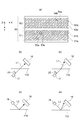
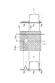
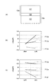
図3に示されるように、エリアセンサ16は、偏光フィルム110の一方の主面110a(第2の主面)側において、幅方向Xに互いに離間して配置される。エリアセンサ16のそれぞれは、二次元状の撮像領域Rを有する。撮像領域Rは、幅方向Xにおいて隣接する撮像領域Rの一部と重複する(図4参照)。エリアセンサ16は、撮像素子19を有する。撮像素子19は、透過光受光領域19a(第1の受光領域)と、反射光受光領域19b(第2の受光領域)と、を有する。エリアセンサ16の撮像領域Rは二次元状であるので、ラインセンサと比べると搬送方向Yにおける視野が広い。そうすると、この視野内における偏光フィルム110に透過光L1と反射光L2とが照射されたような画像を得ることができる。要するに、エリアセンサ16によれば複数の光源から出射された照明光を1個のセンサで観察できる。
As shown in FIG. 3, the
ここで、撮像領域Rは、偏光フィルム110に設定される領域であるが、偏光フィルム110の特定の位置に設定されるものではない。また、図4に示されるように、撮像領域Rは、透過光画像を取得するための透過領域R1(第1の撮像領域部)と、反射光画像を取得するための反射領域R2(第2の撮像領域部)と、を含む。透過領域R1と反射領域R2とは、搬送方向Yに沿って撮像領域Rを分割するように設定される。具体的には、搬送方向Yにおいて上流側に反射領域R2が設定され、下流側に透過領域R1が設定される。この反射領域R2は、透過領域R1とは重複しないように設定している。
Here, the imaging region R is a region set on the
図3に示されるように透過領域R1は、撮像領域Rにおいて透過光用光源17から出射された光が透過する部分である。透過光用光源17から出射された光を、単に「透過光L1」と呼ぶ。この「透過光L1」は、透過光用光源17から出射されてエリアセンサ16に入射するまでの光を意味する。従って、「透過光L1」は、偏光フィルム110を透過する前の光と、偏光フィルム110を透過した後の光と、の両方を含むものとする。反射領域R2は、撮像領域Rにおいて反射光用光源18から出射された光が反射される部分である。反射光用光源18から出射された光を、単に「反射光L2」と呼ぶ。この「反射光L2」は、反射光用光源18から出射されてエリアセンサ16に入射するまでの光を意味する。従って、「反射光L2」は、偏光フィルム110で反射する前の光と、偏光フィルム110で反射された後の光と、の両方を含むものとする。
As shown in FIG. 3, the transmissive region R <b> 1 is a portion through which light emitted from the transmitted
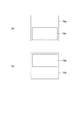
透過光用光源17は、透過光像を得るための透過光L1を偏光フィルム110に対して出射する。透過光用光源17は、偏光フィルム110の組成及び性質に影響を与えない光を発する光源部17aを含む。光源部17aには、例えば、蛍光灯(特に高周波蛍光灯)、メタルハライドランプ、ハロゲン伝送ライト、発光ダイオード(LED)などが挙げられる。
The transmitted
透過光用光源17は、偏光フィルム110の他方の主面110b(第1の主面)側に配置される。すなわち、透過光用光源17は、偏光フィルム110に対しエリアセンサ16と反対側に配置される。透過光用光源17は、主面110bから所定距離だけ離間して配置される。透過光用光源17は、偏光フィルム110への透過光L1の入射角度αが所定の角度になるように配置される。この入射角度αは、一例として30度以上60度以下である。このように、偏光フィルム110への透過光L1の入射角度αが90度でない場合には、入射角度αが0度である場合と比べると、偏光フィルム110内における透過光L1の光路長が長くなる。そうすると、透過光L1が欠陥を通過する際に拡散しやすくなる。従って、拡散透過光により検出される欠陥の検出能力が向上する。透過光L1は、二次元状の広がりを有する光である。幅方向Xにおける透過光L1の長さは、偏光フィルム110の幅よりも大きい。なお、透過光L1の幅方向は、偏光フィルム110の幅方向Xに厳密に一致する必要はなく、搬送方向Yに対して傾いていてもよい。
The transmitted
透過光用光源17と偏光フィルム110との間には、拡散透過画像を得るための遮光板21が配置してもよい。遮光板21は、透過光用光源17と偏光フィルム110との間において、透過光L1の一部を遮るように配置される。遮光板21は、エリアセンサ16からみて、搬送方向Yにおける透過領域R1の半分が隠れるように配置される(ナイフエッジ)。なお、遮光板21は、偏光フィルタであって、偏光フィルム110とクロスニコル状態を形成するように配置されてもよい。
A
ここで、遮光板21を搬送方向Yにおける透過領域R1の半分が隠れるように配置した際の透過光L1に基づく透過光像について説明する。図5の(a)部に示されるように、エリアセンサ16で得られた画像50は、明暗部51を含む。明暗部51は、明部51aと暗部51bとを含む。明部51aには、正透過光像53aが現れることがある。暗部51bには、透過散乱光像53bが現れることがある。正透過光像53aは、透過光用光源17から出射され、偏光フィルム110を透過した後に、エリアセンサ16に垂直に入射した光に基づく像である(図5の(b)部参照)。透過散乱光像53bは、透過光用光源17から出射され、偏光フィルム110を透過するときに散乱され、その後、エリアセンサ16に入射した光に基づく像である(図5の(c)部参照)。
Here, a transmitted light image based on the transmitted light L1 when the
図3に示されるように、反射光用光源18は、偏光フィルム110に対して反射光像を得るための反射光L2を出射する。反射光用光源18は、偏光フィルム110の一方の主面110a(第2の主面)側に配置される。すなわち、反射光用光源18は、偏光フィルム110に対しエリアセンサ16と同じ側に配置される。反射光用光源18は、一方の主面110aから所定距離だけ離間して配置される。透過光用光源17は、偏光フィルム110への反射光の入射角度βが所定の角度になるように配置される。この入射角度βは、一例として30度以上60度以下である。なお、入射角度βは、透過光L1の入射角度αと同じ値であってもよい。透過光用光源17は、幅方向Xに延在する反射光L2を出射する。
As shown in FIG. 3, the reflected
反射光用光源18は、明暗パターンを生じさせる反射光L2を出射する。反射光用光源18は、光源部18aとスリット部22とを有する。光源部18aには、偏光フィルム110の組成及び性質に影響を与えない光を発する光源が利用される。光源には、例えば、蛍光灯(特に高周波蛍光灯)、メタルハライドランプ、ハロゲン伝送ライト、発光ダイオード(LED)などが挙げられる。スリット部22は、透光性を有する樹脂基板22aと、遮光性を有する帯状の遮光部22bとを有する。遮光部22bは、幅方向Xに延在する帯状の部材である。樹脂基板22a上には、遮光部22bの延在方向と直交する方向に複数の遮光部22bが互いに離間するように設けられる。遮光部22bの幅と、遮光部22b同士の間隔とは、略同等である。一例として、これらの幅は、0.1mm以上3mm以下である。
The reflected
光源部18aから出射された光は、スリット部22に入射する。スリット部22では、遮光部22bにおいて光が遮断され、遮光部22bの間から光が透過する。従って、反射光用光源18から出射された反射光L2は、幅方向Xに延びる明部52aと暗部52bとが交互に形成された縞状の明暗パターンを有する。この反射光L2は、明部52aと暗部52bとの境界が反射領域R2において少なくとも1カ所以上形成される。
The light emitted from the
なお、反射光用光源18は、偏光フィルム110の一方の主面に光を出射できれば、特に構成に限定はされない。すなわち、反射光用光源18は、単一光源でも良いし、幅方向Xに延在する複数の線状光源を有してもよい。線状光源は、延在方向と直交する方向に互いに離間して配置される。
The configuration of the reflected
ここで、反射光L2に基づく反射光像について説明する。図5の(a)部に示されるように、エリアセンサ16で得られた画像50は、明暗部52を含む。明暗部52は、複数の明暗パターンを有する縞状の画像である。明暗部52は、明部52aと暗部52bとを含む。明部52aに現れる正反射光像54aは、反射光用光源18から出射され、偏光フィルム110で反射した後に、エリアセンサ16に垂直に入射した光に基づく像である(図5の(d)部参照)。暗部52bに現れる反射散乱光像54bは、反射光用光源18から出射され、偏光フィルム110で反射するときに散乱され、その後、エリアセンサ16に入射した光に基づく像である(図5の(e)部参照)。この反射散乱光とは、入射角度βとは異なる出射角度を有する方向に進行する光をいう。
Here, a reflected light image based on the reflected light L2 will be described. As shown in part (a) of FIG. 5, the
ところで、偏光フィルム110は、搬送中に僅かにゆがむことがある。偏光フィルム110がゆがむと、反射光L2の入射角度βが変化する。そうすると、エリアセンサ16に対する反射光L2の入射位置が変わってしまう。ここで欠陥検査用撮像装置12は、エリアセンサ16を備えているので、搬送方向Yに沿って広がる視野が確保される。従って、搬送中の偏光フィルム110にゆがみが生じた場合であっても、常に、明部52aと暗部52bとの境界を視野に含めることができる。さらに、反射光用光源18は、明暗部52を有するいわゆるパターン照明である。この照明によれば、反射光像内において搬送方向Yに沿って複数の明部52aと暗部52bとが繰り返し現れる。そうすると、搬送中の偏光フィルム110にゆがみが生じて、エリアセンサ16に対する反射光L2の入射位置が変わった場合であっても、いくつかの明暗部52を常に視野内に含めることができる。
By the way, the
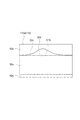
ところで、透過光L1は、いわゆる白色光であり、互いに異なる波長を有する光が合波されたものである。同様に、反射光L2も、いわゆる白色光であり、互いに異なる波長を有する光が合波されたものである。白色光である透過光L1と反射光L2の波長帯域は、互いに重複する波長帯域を有していれば、完全に一致していなくてもよい。透過光L1の波長帯域と反射光L2の波長帯域との関係は、例えば図6の(a)部のように、互いの一部が重複していてもよいし、図6の(b)部に示されるように透過光L1の波長帯域に反射光L2の波長帯域が包含されていてもよく、さらに、図6の(c)部に示されるように反射光L2の波長帯域に透過光L1の波長帯域が包含されていてもよい。 By the way, the transmitted light L1 is so-called white light, which is obtained by combining lights having different wavelengths. Similarly, the reflected light L2 is also so-called white light, which is obtained by combining lights having different wavelengths. The wavelength bands of the transmitted light L1 and reflected light L2, which are white light, do not have to be completely matched as long as they have overlapping wavelength bands. Regarding the relationship between the wavelength band of the transmitted light L1 and the wavelength band of the reflected light L2, for example, as shown in part (a) of FIG. 6, a part of each other may overlap, or part (b) of FIG. As shown in FIG. 6, the wavelength band of the reflected light L2 may be included in the wavelength band of the transmitted light L1, and further, the transmitted light L1 is included in the wavelength band of the reflected light L2 as shown in part (c) of FIG. May be included.
このように、透過光L1及び反射光L2が白色光で有る場合には、エリアセンサ16に入射される光量が増加する。従って、光量が増加していることから、信号強度が高くなるので、欠陥を検出しやすい。また、露出時間を短くすることが可能になるので、偏光フィルム110の搬送速度の増加に対応することができる。また、白色光であり、互いに重複する波長帯域を有する透過光L1と反射光L2とによれば、透過光L1に基づいて得られる透過光像と反射光L2に基づいて得られる反射光像との撮像条件を揃えることができる。従って、透過光像から得られる情報と反射光像から得られる情報とを関連付けた欠陥の検出が可能になる。
Thus, when the transmitted light L1 and the reflected light L2 are white light, the amount of light incident on the
次に、本発明の実施形態に係る欠陥検査方法及び欠陥検査用撮像方法について説明する。欠陥検査方法及び欠陥検査用撮像方法は、複数のエリアセンサ16、透過光用光源17及び反射光用光源18を配置する第1の工程と、偏光フィルム110を搬送させる第2の工程と、透過光L1を出射する第3の工程と、反射光L2を出射する第4の工程と、偏光フィルム110を撮像する第5の工程と、欠陥を検出する第6の工程と、目印Mを施す第7の工程と、を有する。偏光フィルム110を搬送する工程が連続的に実施される期間において、透過光L1を出射する工程及び反射光L2を出射する工程が連続的に実施される。そして、予め設定されたタイミングに基づいて偏光フィルム110を撮像する工程が実施される。偏光フィルム110を撮像する工程が実施されるごとに、欠陥を検出する工程と目印Mを施す工程とが実施される。
Next, a defect inspection method and a defect inspection imaging method according to an embodiment of the present invention will be described. The defect inspection method and the defect inspection imaging method include a first step of arranging a plurality of
まず、搬送手段11は、搬送方向Yに沿って偏光フィルム110を移送する。この工程は、偏光フィルム110の製造中において、連続的に実施される。搬送中の偏光フィルム110に対して、透過光用光源17から透過光L1を出射する。また、搬送中の偏光フィルム110に対して、反射光用光源18から反射光L2を出射する。
First, the
欠陥検査用撮像装置12は、搬送中における偏光フィルム110の撮像領域Rを撮像する。そして、欠陥検査用撮像装置12は、撮像により得られた二次元画像を画像解析装置13に送信する。エリアセンサ16は、所定の時間間隔ごとに撮像領域Rを撮像する。この時間間隔は、エリアセンサ16が撮像した二次元画像の搬送方向Yの長さが、エリアセンサ16が二次元画像を取り込んでから次の二次元画像を取り込むまでの区間に偏光フィルム110が搬送される搬送距離の少なくとも2倍以上になる時間である。すなわち、撮像の時間間隔は、偏光フィルム110の同一領域を2回以上撮像可能な時間間隔であり、ある欠陥が透過光による撮像領域と反射光による撮像領域を最低1回以上通過した状態を撮像することができる。この時間間隔によれば、二次元画像の搬送方向Yの長さを、画像取込区間における搬送距離よりも大きくし、偏光フィルム110の同一部分の撮像数を増加させることにより、高精度に欠陥を検査できる。
The defect
画像解析装置13は、二次元画像に対して欠陥の検出処理を実施する。欠陥の処理は、透過画像に適用される処理と、反射画像に適用される処理とがある。
The
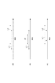
まず、図7の(a)部〜(e)部を参照しつつ、透過画像に適用される処理について説明する。この処理は、ライン合成と呼ばれる処理と、ライン合成処理により得られた画像から欠陥を検出する処理とを含む。 First, processing applied to a transparent image will be described with reference to parts (a) to (e) in FIG. This process includes a process called line synthesis and a process for detecting a defect from an image obtained by the line synthesis process.
エリアセンサ16は所定のフレームレートで撮像領域Rの撮像を行う。その結果、図7の(a)部に示されるような画像群(画像G1,G2,G3,G4)が得られる。図7の(a)部における画像G1の撮像タイミングは時刻t1(t)であり、画像G2の撮像タイミングは時刻t2(t+Δt)であり、画像G3の撮像タイミングは時刻t3(t+2×Δt)であり、画像G4の撮像タイミングは時刻t4(t+3×Δt)である。それぞれの画像G1,G2,G3,G4には、線状の欠陥Dが含まれる。偏光フィルム110が搬送方向Yに移動するので、欠陥Dも搬送方向Yに移動するように見えている。また、この例では、透過散乱光は生じていないものとして考える。従って、暗部51bには、欠陥Dは現れていない。
The
それぞれの画像G1,G2,G3,G4を搬送方向Yに沿って4個のラインに分割する(図7の(b)部参照)。次に、画像群Gにおける同じ位置に対応するライン(例えば、ラインG1a,G2a,G3a,G4a参照)を選択する。この選択は、単位時間ごとに同じ行のラインを抜き出すものともいえる。そして、選択したラインG1a,G2a,G3a,G4aを搬送方向Yに沿って繋ぎ合わせる(図7の(c)部参照)。合成画像G5は、1番目のラインを撮像するラインセンサが撮像した画像と同等の画像であり、合成画像G6は、2番目のラインを撮像するラインセンサが撮像した画像と同等の画像である。同様に、合成画像G7は、3番目のラインを撮像するラインセンサが撮像した画像と同等の画像であり、合成画像G8は、4番目のラインを撮像するラインセンサが撮像した画像と同等の画像である。このように、エリアセンサ16が撮像した時系列における複数の画像から同じ位置のラインを選択してそれらを結合する処理をライン合成処理と呼ぶ。このライン合成処理は、空間的な積算処理であるとも言える。
Each of the images G1, G2, G3, and G4 is divided into four lines along the conveyance direction Y (see the part (b) in FIG. 7). Next, a line corresponding to the same position in the image group G (for example, see the lines G1a, G2a, G3a, and G4a) is selected. This selection can also be said to extract the same line in every unit time. Then, the selected lines G1a, G2a, G3a, and G4a are joined along the transport direction Y (see the part (c) in FIG. 7). The composite image G5 is an image equivalent to an image captured by the line sensor that captures the first line, and the composite image G6 is an image equivalent to an image captured by the line sensor that captures the second line. Similarly, the composite image G7 is an image equivalent to the image captured by the line sensor that captures the third line, and the composite image G8 is an image equivalent to the image captured by the line sensor that captures the fourth line. It is. In this way, a process of selecting lines at the same position from a plurality of images in time series captured by the
次に、図7の(d)部に示されるように、画像解析装置13は、合成画像に対して欠陥Dを強調する処理を行う。この処理により、処理画像G5A,G6A,G7A,G8Aを得る。この処理には、垂直微分フィルタ法や、二値化法などが利用される。例えば、二値化法には、ラプラシアンヒストグラム法を用いて固定した閾値が利用される。
Next, as illustrated in part (d) of FIG. 7, the
次に、図7の(e)部に示されるように、画像解析装置13は、欠陥Dが強調された画像をさらに重ね合わせる。処理画像G5A,G6A,G7A,G8Aに含まれた偏光フィルム110の撮像範囲は、搬送方向Yにおいて一部が重複しつつも互いに異なる。画像解析装置13は、重複した部分を利用して処理画像G5A,G6A,G7A,G8Aを積算処理し、1枚の合成画像G9を生成する。この積算処理は、時間的な積算処理であるともいえる。また、この処理によれば、明視野から暗視野に至る様々な光学条件で撮像された画像が積算される。従って、異物の検出能力がさらに高まる。さらに、上述した処理は、複数台のラインセンサを使用した場合の処理と同等の結果であるともいえる。
Next, as illustrated in part (e) of FIG. 7, the
次に、合成画像G9を利用して欠陥Dを検出する処理を行う。この処理には、特徴量に基づく検出法が用いられる。画像解析装置13は、欠陥Dの態様と、その欠陥Dが画像として捉えられたときの特徴とを関連付けたデータを有する。このデータは教師データとも呼ばれる。画像解析装置13は、まず、合成画像G9の特徴量を算出する。続いて、画像解析装置13は、算出された特徴量と教師データとを比較することにより、もっとも関連性が高い教師データを選択する。そして、画像解析装置13は、合成画像に含まれた欠陥Dが選択された教師データに関連付けられた態様の欠陥であると判断する。
Next, a process for detecting the defect D using the composite image G9 is performed. For this process, a detection method based on a feature amount is used. The
特徴量には、画像全体から取得可能な種々の値がある。例えば、種々の値には、輝度合計値、輝度平均、輝度中央値、輝度分散、輝度勾配方向、輝度勾配強度がある。また、特徴量として、画像における欠陥から取得可能な種々の値も利用し得る。この欠陥から取得可能な値には、欠陥面積、欠陥周囲長さ、欠陥円形度、欠陥フェレ径、欠陥縦横比などがある。 There are various values that can be acquired from the entire image. For example, the various values include a luminance total value, luminance average, luminance median value, luminance dispersion, luminance gradient direction, and luminance gradient intensity. Various values that can be acquired from defects in the image can also be used as the feature amount. Values that can be acquired from the defect include a defect area, a defect perimeter, a defect circularity, a defect Ferre diameter, and a defect aspect ratio.
なお、教師データは、予め記録されたデータに対して新たに取得されたデータを適用することを必要に応じて実施してもよい。このデータ更新によれば、特徴量と欠陥態様との関連度が高まる。また、特徴量と欠陥態様との関連は、ニューラルネットワークや機械学習などの手法を用いて得ることが可能である。 The teacher data may be applied as necessary to newly acquired data with respect to previously recorded data. According to this data update, the degree of association between the feature amount and the defect mode increases. Further, the relationship between the feature amount and the defect mode can be obtained by using a technique such as a neural network or machine learning.
以上の処理により、透過画像から欠陥が検出される。なお、上述した処理は、反射画像に適用されてもよい。 Through the above processing, the defect is detected from the transmission image. Note that the processing described above may be applied to a reflected image.
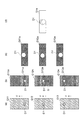
次に、図8の(a)部〜(d)部を参照しつつ、反射画像に適用される処理について説明する。 Next, processing applied to the reflected image will be described with reference to the (a) to (d) portions of FIG.
エリアセンサ16は所定のフレームレートで撮像領域Rの反射画像を得る。その結果、図8の(a)部に示されるような反射画像群が得られる。それぞれの画像には、欠陥D1が含まれる。反射画像G11の撮像タイミングは時刻t1(t)であり、反射画像G12の撮像タイミングは時刻t2(t+Δt)であり、反射画像G13の撮像タイミングは時刻t3(t+2×Δt)である。これらの反射画像G11,G12,G13に対して、欠陥D1を強調する処理を行う。この処理により、処理画像G11A,G12A,G13Aが得られる(図8の(b)部参照)。この処理には、垂直微分フィルタ法や、二値化法などが利用される。
The
次に、処理画像G11A,G12A,G13Aに対して欠陥D1を検出する処理を行う。この欠陥D1を検出する処理は、欠陥D1の態様に対応した複数のアルゴリズムを含む。例えば、欠陥D1の一例である打痕の検出に対応するアルゴリズムを説明する。図9は、図8の(b)部における処理画像G12Aの領域Sを拡大して示す図である。処理画像G12Aにおいて搬送方向Yに沿った輝度分布を取得する。例えば、ラインA1上には打痕D1aが存在しない。このラインA1における輝度分布は、グラフT1に示される。グラフT1は、明部52aに対応する部分T1aと、暗部52bに対応する部分T1bと、を有する。一方、ラインA2上には打痕D1aが存在する。打痕D1aが存在する領域では、輝度分布が乱れることがある。ラインA2における輝度分布は、グラフT2に示される。グラフT2を参照すると、暗部52bに対応する部分T2bにおいて、ピークPが存在する。このピークPは打痕D1aの存在を示すものとして考えられる。そして、ピークPの値が閾値以上である場合に、画像解析装置13は打痕D1aが存在すると判断する。
Next, processing for detecting the defect D1 is performed on the processed images G11A, G12A, and G13A. The process of detecting the defect D1 includes a plurality of algorithms corresponding to the form of the defect D1. For example, an algorithm corresponding to detection of a dent that is an example of the defect D1 will be described. FIG. 9 is an enlarged view showing the region S of the processed image G12A in the part (b) of FIG. In the processed image G12A, a luminance distribution along the transport direction Y is acquired. For example, the dent D1a does not exist on the line A1. The luminance distribution in the line A1 is shown in the graph T1. The graph T1 includes a portion T1a corresponding to the
別の例として、欠陥D1の一例である凹みの検出に対応するアルゴリズムを説明する。図10に示されるように偏光フィルム110の主面110aは理想的には平面である。従って、平面である領域における明部52aと暗部52bとの境界線52cは直線状である。なお、境界線52cは、明部52aのエッジ又は暗部52bのエッジであるともいえる。一方、偏光フィルム110の主面110aに凹みD1bが存在する場合、この凹みD1bを含む領域に投影された境界線52dはゆがむ。この境界線52dのゆがみを検出することにより、凹みD1bを検出することが可能になる。例えば、処理画像G11A,G12A,G13Aにおいて境界線52dの形状に対応するエッジプロファイルを検出する。そして、エッジプロファイルにおいて、閾値以上のピークが存在する場合には、凹みが存在するとして判断する。なお、この処理には、エッジプロファイルから歪曲度を算出し、閾値と比較する手法を用いてもよい。
As another example, an algorithm corresponding to detection of a dent, which is an example of the defect D1, will be described. As shown in FIG. 10, the
次に、図8の(c)部に示されるように、それぞれの処理画像G11A,G12A,G13Aから欠陥D1が検出されたライン画像G11a,G12a,G13aを抜き出す。次に、図8の(d)部に示されるように、抜き出したライン画像G11a,G12a,G13aを重ね合わせることにより、合成画像G14を得る。この合成画像G14では、凹みD1bが搬送方向Yに沿って延びるように示される。そして、経時的に得られた複数の画像において、欠陥が検出された画像の数が多いほど、搬送方向Yに沿う長さが長くなる。従って、欠陥の検出率が高まる。 Next, as shown in part (c) of FIG. 8, line images G11a, G12a, and G13a in which the defect D1 is detected are extracted from the processed images G11A, G12A, and G13A. Next, as shown in part (d) of FIG. 8, the extracted line images G11a, G12a, and G13a are superimposed to obtain a composite image G14. In the composite image G14, the recess D1b is shown to extend along the transport direction Y. In the plurality of images obtained over time, the length along the conveyance direction Y increases as the number of images in which defects are detected increases. Therefore, the defect detection rate increases.
以上の処理により、反射画像から欠陥が検出される。なお、上述した処理は、透過画像に適用されてもよい。 Through the above processing, defects are detected from the reflected image. Note that the above-described processing may be applied to a transparent image.
なお、欠陥の検出処理に用いられるアルゴリズムは、上述したアルゴリズムに限定されず、検出対象である欠陥の態様に応じたアルゴリズムを適用してよい。複数のアルゴリズムを適用することにより、検出可能な欠陥の態様数を増やせる。従って、欠陥の検出能力がさらに高まる。 The algorithm used for the defect detection process is not limited to the above-described algorithm, and an algorithm according to the mode of the defect to be detected may be applied. By applying a plurality of algorithms, the number of detectable defect modes can be increased. Therefore, the defect detection capability is further enhanced.
次に、画像解析装置13は、検出された欠陥に関するデータを利用して欠陥検査情報を作成する。欠陥検査情報は、欠陥の種類と、欠陥の位置に関する情報を含む。また、欠陥検査情報は、1個のロットに対する欠陥の有無を示す情報などを含んでもよい。欠陥検査情報の一例には、偏光フィルム110の全領域の欠陥マップが挙げられる。
Next, the
次に、マーキング装置14は、欠陥検査情報を利用して、偏光フィルム110に欠陥の存在を示す目印Mを付す。この目印Mは、目視やその他の手段によって確認可能である。この欠陥位置を示す目印Mは、例えば、偏光フィルム110を所定サイズの枚葉品に裁断した後に、枚葉品を正常品と欠陥品とに分別する処理に利用される。
Next, the marking
以下、本実施形態に係る欠陥検査用撮像装置12、欠陥検査システム10、フィルム製造装置100、欠陥検査用撮像方法、欠陥検査方法及びフィルム製造方法の作用効果について説明する。
Hereinafter, the effects of the defect
この欠陥検査用撮像装置1では、偏光フィルム110を透過した透過光L1がエリアセンサ16の透過光受光領域19aに入射するように透過光用光源17が配置される。また、偏光フィルム110で反射した反射光L2がエリアセンサ16の反射光受光領域19bに入射するように反射光用光源18が配置される。そうすると、エリアセンサ16によれば、透過光L1に基づく部分である透過光像、及び、反射光L2に基づく部分である反射光像を含む画像が得られる。この画像によれば、透過光像から得られる情報と反射光像から得られる情報とを利用して欠陥の検出に利用できる。従って、欠陥検査用撮像装置1は、欠陥の検出に利用できる測定値のバリエーションが多くなるので、取得可能な欠陥に関する情報量を増大させることができる。従って、異なる態様の欠陥を検出する能力を向上させることができる。
In this defect inspection imaging apparatus 1, the transmitted
透過光L1に基づく画像は、さらに、正透過光に基づく画像と、透過散乱光に基づく画像とを含む。正透過光及び透過散乱光に基づく画像によれば、付着異物による傷の転写といった偏光フィルム110の変形、及び、偏光フィルム110に混入又は付着した異物などを好適に検出できる。また、反射光L2に基づく画像は、さらに、正反射光に基づく画像と、反射散乱光に基づく画像とを含む。正反射光及び反射散乱光に基づく画像によれば、付着異物による傷の転写といった偏光フィルム110の変形、偏光フィルム110に混入又は付着した異物、及び貼り合せ時に生じ得る噛み込みによる気泡などを好適に検出できる。
The image based on the transmitted light L1 further includes an image based on the regular transmitted light and an image based on the transmitted scattered light. According to the image based on the regular transmitted light and the transmitted scattered light, it is possible to suitably detect the deformation of the
本実施形態に係る欠陥検査用撮像装置12によれば、1個のエリアセンサ16が透過光像と反射光像とを含む画像を得る。従って、透過光像を得るためのエリアセンサと反射光像を得るためのエリアセンサとをそれぞれ準備する必要がない。従って、欠陥検査用撮像装置12の構成を簡易にすることができる。また、欠陥検査用撮像装置12を構成する装置の数の増加が抑制されるので、フィルム製造装置100における欠陥検査用撮像装置12の配置の自由度を高めることができる。
According to the defect
なお、上述した実施形態は本発明に係る欠陥検査用撮像装置の一例を示すものである。本発明に係る欠陥検査用撮像装置は、実施形態に係る欠陥検査用撮像装置に限られるものではなく、各請求項に記載した要旨を変更しない範囲で、実施形態に係る欠陥検査用撮像装置を変形し、又は他のものに適用したものであってもよい。 The embodiment described above shows an example of an imaging apparatus for defect inspection according to the present invention. The imaging apparatus for defect inspection according to the present invention is not limited to the imaging apparatus for defect inspection according to the embodiment, and the imaging apparatus for defect inspection according to the embodiment is within a range not changing the gist described in each claim. It may be modified or applied to others.
例えば、上記実施形態では、透過光像、又は、反射光像のいずれか一方を用いて欠陥を検出する例を説明した。例えば、欠陥の検出においては、透過光像及び反射光像の両方を利用してもよい。換言すると、透過光像から得られる欠陥信号と反射光像から得られる欠陥信号との関係に基づいて欠陥を検出してもよい。このような欠陥信号の関係を利用することにより、欠陥の有無の判別に加えて、欠陥の位置や種別といった情報を得ることができる。 For example, in the above-described embodiment, an example has been described in which a defect is detected using either a transmitted light image or a reflected light image. For example, in detecting a defect, both a transmitted light image and a reflected light image may be used. In other words, the defect may be detected based on the relationship between the defect signal obtained from the transmitted light image and the defect signal obtained from the reflected light image. By utilizing such a relationship of defect signals, information such as the position and type of the defect can be obtained in addition to the determination of the presence or absence of the defect.
具体的には、図11に示されるように、偏光フィルム110が欠陥の種別として上気泡201、下気泡202及び異物203を含む場合を想定する。また、上気泡201及び下気泡202の位置として、偏光フィルム110の厚み方向における位置を想定する。上気泡201とは、偏光フィルム本体部111の一方の側に配置されたセパレートフィルム付き粘着材112と偏光フィルム本体部111との間、或いは、セパレートフィルム付き粘着材112に含まれた気泡である。下気泡202とは、偏光フィルム本体部111の他方の側に配置された保護フィルム113と偏光フィルム本体部111との間、或いは、保護フィルム113に含まれた気泡である。なお、「上気泡」及び「下気泡」は、説明の便宜上用いるものであり、上記の態様に限定されることはない。また、異物203の位置は、図11に示された位置に限定されることはなく、セパレートフィルム付き粘着材112及び保護フィルム113に含まれていてもよいし、偏光フィルム本体部111とセパレートフィルム付き粘着材112及び保護フィルム113との間であってもよい。
Specifically, as illustrated in FIG. 11, it is assumed that the
図12の(a)部は、透過光受光領域19aと反射光受光領域19bとの関係を示し、図12の(b)部は、欠陥と欠陥信号との関係を示す。欠陥信号としては、例えば、輝度が挙げられる。グラフP12aは、欠陥が上気泡201であるときの透過光像から得られる欠陥信号(以下「透過欠陥信号」とも言う)と反射光像から得られる欠陥信号(以下「反射欠陥信号」とも言う)との関係を示す。グラフP12bは、欠陥が下気泡202であるときの透過欠陥信号と反射欠陥信号との関係を示す。グラフP12cは、欠陥が異物203であるときの透過欠陥信号と反射欠陥信号との関係を示す。
12A shows the relationship between the transmitted
グラフP12a,P12b,P12cを参照すると、欠陥の種類や位置に対応して、透過欠陥信号と反射欠陥信号との関係が異なっていることがわかる。具体的には、透過欠陥信号が負であり、且つ、反射欠陥信号が正である場合には、欠陥は、気泡であると判別できる。さらに、透過欠陥信号の絶対値と反射欠陥信号の絶対値とを比較したとき、透過欠陥信号の絶対値よりも反射欠陥信号の絶対値が大きい場合には、欠陥は、上気泡201であると判別できる。一方、透過欠陥信号の絶対値と反射欠陥信号の絶対値とが同等である場合には、欠陥は、下気泡202であると判別できる。さらに、透過欠陥信号が負であり、且つ反射欠陥信号も負である場合には、欠陥は異物であると判別できる。なお、欠陥が異物であるとき、透過欠陥信号の絶対値は、反射欠陥信号の絶対値よりも大きい。
Referring to the graphs P12a, P12b, and P12c, it can be seen that the relationship between the transmission defect signal and the reflection defect signal differs according to the type and position of the defect. Specifically, when the transmission defect signal is negative and the reflection defect signal is positive, it can be determined that the defect is a bubble. Further, when the absolute value of the transmission defect signal is compared with the absolute value of the reflection defect signal, if the absolute value of the reflection defect signal is larger than the absolute value of the transmission defect signal, the defect is the
従って、透過欠陥信号と反射欠陥信号との関係を利用することにより、欠陥の位置や種別といった情報を得ることができる。なお、このような判別処理は、画像解析装置13によって行われる。従って、画像解析装置13は、透過光像から透過欠陥信号を得る工程を実施する手段と、透過欠陥信号の特徴を示す第1の情報を得る工程を実施する手段と、反射光像から反射欠陥信号を得る工程を実施する手段と、反射欠陥信号の特徴を示す第2の情報を得る工程を実施する手段と、第1の情報と第2の情報とを利用して欠陥に関する情報を得る工程を実施する手段と、を有する。透過欠陥信号の特徴を示す第1の情報とは、透過欠陥信号のピーク値、当該ピーク値の絶対値、及び、ピーク値の正負の符号に関する情報である。反射欠陥信号の特徴を示す第2の情報とは、反射欠陥信号のピーク値、当該ピーク値の絶対値、及び、ピーク値の正負の符号に関する情報である。欠陥に関する情報とは、欠陥の種類を示す情報及び欠陥の位置を示す情報である。
Therefore, information such as the position and type of the defect can be obtained by using the relationship between the transmission defect signal and the reflection defect signal. Note that such determination processing is performed by the
また、上記実施形態では、透過光受光領域19aと反射光受光領域19bとが互いに重複しない構成(図12の(a)部参照)を例に説明した。例えば、図13の(a)部に示されるように、透過光受光領域19aと反射光受光領域19bとはそれぞれの一部が互いに重複していてもよい。この場合には、領域N1から透過光像が得られ、領域N2から反射光像が得られると共に領域N3から透過光と反射光とに基づく合成光像とを得られる。なお、撮像領域Rにおける透過領域R1と反射領域R2とは互いに重複していてもよい。また、透過光用光源17と反射光用光源18の照射幅や照射位置の設定によっては、撮像領域Rにおける透過領域R1と反射領域R2とは互いに重複していなくてもよい。そして、これらの透過光像、反射光像及び合成光像から、透過欠陥信号、反射欠陥信号及び合成欠陥信号をそれぞれ得ることができる。従って、欠陥の検出においては、3個の欠陥信号から2個又は3個を組み合わせた処理により、欠陥に関する情報をより多く得ることが可能になる。例えば、透過欠陥信号と反射欠陥信号とを利用して、欠陥の種別とその位置を判別することができる。また、透過欠陥信号と合成欠陥信号とを利用した判別や、反射欠陥信号と合成欠陥信号とを利用した判別を行うこともできる。
In the above embodiment, the transmitted
図13の(b)部は、欠陥と欠陥信号との関係を示す。図13の(b)部における欠陥信号は、透過欠陥信号及び合成欠陥信号である。図13の(b)部に示されるように、透過欠陥信号が負であり、且つ、合成欠陥信号が正である場合には、欠陥は、気泡であると判別できる。さらに、透過欠陥信号の絶対値と合成欠陥信号の絶対値とを比較したとき、透過欠陥信号の絶対値よりも合成欠陥信号の絶対値が大きい場合には、欠陥は、上気泡201であると判別できる。一方、透過欠陥信号の絶対値と合成欠陥信号の絶対値とが同等である場合には、欠陥は、下気泡202であると判別できる。さらに、透過欠陥信号が負であり、且つ合成欠陥信号も負である場合には、欠陥は異物であると判別できる。なお、欠陥が異物であるとき、透過欠陥信号の絶対値は、合成欠陥信号の絶対値よりも小さい。
Part (b) of FIG. 13 shows the relationship between defects and defect signals. The defect signals in part (b) of FIG. 13 are a transmission defect signal and a composite defect signal. As shown in part (b) of FIG. 13, when the transmission defect signal is negative and the composite defect signal is positive, it can be determined that the defect is a bubble. Further, when the absolute value of the transmission defect signal is compared with the absolute value of the composite defect signal, if the absolute value of the composite defect signal is larger than the absolute value of the transmission defect signal, the defect is the
図13の(c)部は、欠陥と欠陥信号との関係を示す。図13の(c)部における欠陥信号は、反射欠陥信号及び合成欠陥信号である。図13の(c)部に示されるように、反射欠陥信号が正であり、且つ、合成欠陥信号が正である場合には、欠陥は、気泡であると判別できる。さらに、反射欠陥信号の絶対値と合成欠陥信号の絶対値とが同等であり、且つ、比較的大きい場合には、欠陥は上気泡201であると判別できる。一方、反射欠陥信号の絶対値と合成欠陥信号の絶対値とが同等であり、且つ、比較的小さい場合には、欠陥は下気泡202であると判別できる。なお、上気泡201に基づく反射欠陥信号の絶対値は、下気泡202に基づく反射欠陥信号の絶対値よりも大きい。さらに、反射欠陥信号が負であり、且つ、反射欠陥信号も負である場合には、欠陥は異物であると判別できる。なお、欠陥が異物であるとき、反射欠陥信号の絶対値は、合成欠陥信号の絶対値よりも小さい。
FIG. 13C shows the relationship between defects and defect signals. The defect signals in part (c) of FIG. 13 are a reflection defect signal and a composite defect signal. As shown in part (c) of FIG. 13, when the reflection defect signal is positive and the combined defect signal is positive, it can be determined that the defect is a bubble. Further, when the absolute value of the reflection defect signal is equal to the absolute value of the combined defect signal and is relatively large, it can be determined that the defect is the
従って、図13の(a)部に示された透過光受光領域19aと反射光受光領域19bとを有する装置によれば、透過欠陥信号、反射欠陥信号及び合成欠陥信号が得られ、これらを組み合わせた評価を行うことにより欠陥に関する情報の量を増加させることができる。これにより、欠陥の種別の判別、欠陥の位置の判別が可能となり、ひいてはそれらの判別の確からしさを向上させることもできる。
Therefore, according to the apparatus having the transmitted
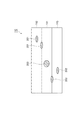
また、透過光受光領域19aと反射光受光領域19bとの関係は、さらに別の関係とすることもできる。例えば、図14の(a)部に示されるように、透過光受光領域19aに反射光受光領域19bが完全に含まれていてもよい。この場合には、透過欠陥信号と合成欠陥信号とが得られ、これらを組み合わせた欠陥の検査を行うことができる(図13の(b)部参照)。さらに、図14の(c)部に示されるように、反射光受光領域19bに透過光受光領域19aが完全に含まれていてもよい。この場合には、反射欠陥信号と合成欠陥信号とが得られ、これらを組み合わせた欠陥の検査を行うことができる(図13の(c)部参照)。
Further, the relationship between the transmitted
要するに、透過光用光源17及び反射光用光源18は、上記構成に限定されることはない。透過光用光源17及び反射光用光源18は、偏光フィルム110上において互いに照射する領域の一部を重複させても良いし、一方の光源により照射される領域が他方の領域に含まれていても良い。そのような構成とすることにより、透過光、反射光のみの欠陥情報以外に透過光と反射光の両方の寄与を受けた欠陥情報をさらに得ることができ、検出可能な欠陥の態様を増やすことができる。例えば、検査対象が偏光フィルムのような積層フィルムの場合、透過光L1と反射光L2との組み合せることにより、検出可能な欠陥の態様が増えるだけでなく、欠陥が存在する層についても識別することができる。例えば、透過光L1と反射光L2で同じ欠陥を検出する場合、反射光L2を照射する側の層に欠陥が存在すること示しており、透過光L1で検出するものの、反射光L2では検出されない欠陥の場合は、反射光L2を照射する側とは反対側(透過光L1の照射側)に欠陥が存在することを示している。
In short, the transmitted
透過光及び反射光は白色光でなくてもよい。例えば、透過光が第1の波長帯域を有する光であり、反射光が、第2の波長帯域を有する光であってもよい。この場合、第1の波長帯域が、第2の波長帯域と重複する帯域を含んでいてもよい。第1及び第2の波長帯域が重複するとは、図6の(a)部〜(c)部で示したような重複形態を含む。互いに重複する波長帯域を有する透過光と反射光とによれば、透過光に基づいて得られる透過光像と反射光に基づいて得られる反射光像との撮像条件を揃えることができる。従って、透過光像から得られる情報と反射光像から得られる情報とを関連付けた欠陥の検出が可能になる。なお、透過光及び反射光が白色光である場合、透過光は第1の波長帯域の光を含み、反射光は、第2の波長帯域の光を含む。 The transmitted light and the reflected light may not be white light. For example, the transmitted light may be light having a first wavelength band, and the reflected light may be light having a second wavelength band. In this case, the first wavelength band may include a band overlapping with the second wavelength band. That the 1st and 2nd wavelength band overlaps includes the duplication form as shown by the (a) part-(c) part of FIG. According to the transmitted light and reflected light having overlapping wavelength bands, the imaging conditions of the transmitted light image obtained based on the transmitted light and the reflected light image obtained based on the reflected light can be made uniform. Accordingly, it is possible to detect a defect in which information obtained from the transmitted light image and information obtained from the reflected light image are associated with each other. When the transmitted light and the reflected light are white light, the transmitted light includes light in the first wavelength band, and the reflected light includes light in the second wavelength band.
10…欠陥検査システム、11…搬送手段、12…欠陥検査用撮像装置、13…画像解析装置、14…マーキング装置、16…エリアセンサ、17…透過光用光源、18…反射光用光源、19…撮像素子、21…遮光板、51…明暗部、51a…明部、51b…暗部、52…明暗部、52a…明部、52b…暗部、100…フィルム製造装置、101,102,103…原反ロール、104,105…貼合ローラ、106…搬送ローラ、110…偏光フィルム、110a…一方の主面、110b…他方の主面、D1…欠陥、D1a…打痕、D1b…凹み、L1…透過光、L2…反射光、M…目印、R…撮像領域、R1…透過領域、R2…反射領域、Y…搬送方向。
DESCRIPTION OF
Claims (14)
前記フィルムの第1の主面側に配置され、前記フィルムに向けて第1の光を出射する第1の光出射手段と、
前記フィルムの第2の主面側に配置され、前記フィルムに向けて第2の光を出射する第2の光出射手段と、
前記第2の主面側に配置され、前記フィルム上に設定された二次元状の撮像領域を撮像する撮像手段と、
前記第1の光出射手段、前記第2の光出射手段及び前記撮像手段に対して前記フィルムを搬送方向へ相対的に搬送させる搬送手段と、を備え、
前記撮像手段は、第1の受光領域と、第2の受光領域とを有し、
前記第1の光出射手段は、前記フィルムを透過した前記第1の光が前記第1の受光領域に入射するように配置され、
前記第2の光出射手段は、前記フィルムにおいて反射した前記第2の光が前記第2の受光領域に入射するように配置され、
前記第1の受光領域及び前記第2の受光領域の少なくとも一方は、他方と重複しない部分を含む、欠陥検査用撮像装置。 An imaging device for film defect inspection,
A first light emitting means arranged on the first main surface side of the film and emitting first light toward the film;
A second light emitting means disposed on the second main surface side of the film and emitting a second light toward the film;
An imaging unit that is disposed on the second main surface side and that images a two-dimensional imaging region set on the film;
A transport unit that transports the film in the transport direction relative to the first light output unit, the second light output unit, and the imaging unit;
The imaging means has a first light receiving region and a second light receiving region,
The first light emitting means is arranged so that the first light transmitted through the film is incident on the first light receiving region,
The second light emitting means is arranged so that the second light reflected by the film enters the second light receiving region,
An imaging device for defect inspection, wherein at least one of the first light receiving region and the second light receiving region includes a portion that does not overlap with the other.
前記第2の光は、第2の波長帯域を有し、
前記第1の波長帯域は、前記第2の波長帯域と重複する帯域を含む、
請求項1に記載の欠陥検査用撮像装置。 The first light has a first wavelength band;
The second light has a second wavelength band;
The first wavelength band includes a band overlapping with the second wavelength band,
The imaging apparatus for defect inspection according to claim 1.
前記第1の光出射手段は、前記フィルムの第1の撮像領域部に対して前記第1の光を出射するように配置され、
前記第2の光出射手段は、前記フィルムの第2の撮像領域部に対して前記第2の光を出射するように配置される、請求項1〜4の何れか一項に記載の欠陥検査用撮像装置。 The imaging region includes a first imaging region unit and a second imaging region unit divided in the transport direction,
The first light emitting means is arranged to emit the first light to the first imaging region portion of the film,
The defect inspection according to any one of claims 1 to 4, wherein the second light emitting unit is arranged to emit the second light to the second imaging region portion of the film. Imaging device.
前記欠陥検査用撮像装置によって得られた画像に基づいて、前記フィルムに存在する欠陥を検出する検出部と、を備える、欠陥検査システム。 An imaging apparatus for defect inspection according to any one of claims 1 to 5,
A defect inspection system comprising: a detection unit that detects a defect present in the film based on an image obtained by the defect inspection imaging device.
第1の受光領域と第2の受光領域とを有する撮像手段に対して前記フィルムを相対的に搬送させる工程と、
前記フィルムに対し前記撮像手段と反対側に配置されると共に、前記フィルムを透過した第1の光が前記第1の受光領域に入射するように配置された第1の光出射手段によって、前記フィルムに向けて前記第1の光を出射する工程と、
前記フィルムに対し前記撮像手段と同じ側に配置されると共に、前記フィルムにおいて反射した第2の光が前記第2の受光領域に入射するように配置された第2の光出射手段によって、前記フィルムに向けて前記第2の光を出射する工程と、
前記撮像手段によって、前記フィルム上に設定された二次元状の撮像領域を撮像する工程と、を有し、
前記第1の受光領域及び前記第2の受光領域の少なくとも一方は、他方と重複しない部分を含む、欠陥検査用撮像方法。 An imaging method for imaging for defect inspection of a film,
Transporting the film relative to an imaging means having a first light receiving area and a second light receiving area;
The film is disposed on the side opposite to the imaging unit with respect to the film, and the first light emitting unit is arranged so that the first light transmitted through the film enters the first light receiving region. Emitting the first light toward
The film is disposed on the same side as the imaging unit with respect to the film, and the second light emitting unit is arranged so that the second light reflected on the film is incident on the second light receiving region. Emitting the second light toward
Imaging the two-dimensional imaging area set on the film by the imaging means,
An imaging method for defect inspection, wherein at least one of the first light receiving region and the second light receiving region includes a portion that does not overlap with the other.
前記第2の光は、第2の波長帯域を有し、
前記第1の波長帯域は、前記第2の波長帯域と重複する帯域を含む、
請求項8に記載の欠陥検査用撮像方法。 The first light has a first wavelength band;
The second light has a second wavelength band;
The first wavelength band includes a band overlapping with the second wavelength band,
The defect inspection imaging method according to claim 8.
前記第1の光を出射する工程では、前記フィルムの第1の撮像領域部に対して前記第1の光を出射し、
前記第2の光を出射する工程では、前記フィルムの第2の撮像領域部に対して前記第2の光を出射する、請求項8〜11の何れか一項に記載の欠陥検査用撮像方法。 The imaging region includes a first imaging region unit and a second imaging region unit divided in the film transport direction,
In the step of emitting the first light, the first light is emitted to the first imaging region portion of the film,
The imaging method for defect inspection according to any one of claims 8 to 11, wherein in the step of emitting the second light, the second light is emitted to a second imaging region portion of the film. .
前記欠陥検査用撮像方法によって撮像された画像に基づいて、前記フィルムに存在する欠陥を検出する工程と、を含む、欠陥検査方法。 An imaging method for defect inspection according to any one of claims 8 to 12,
Detecting a defect present in the film based on an image captured by the imaging method for defect inspection.
A film manufacturing method comprising the defect inspection method according to claim 13.
Priority Applications (1)
| Application Number | Priority Date | Filing Date | Title |
|---|---|---|---|
| JP2016136786A JP2018009800A (en) | 2016-07-11 | 2016-07-11 | Defect inspection imaging device, defect inspection system, film manufacturing apparatus, defect inspection imaging method, defect inspection method, and film manufacturing method |
Applications Claiming Priority (1)
| Application Number | Priority Date | Filing Date | Title |
|---|---|---|---|
| JP2016136786A JP2018009800A (en) | 2016-07-11 | 2016-07-11 | Defect inspection imaging device, defect inspection system, film manufacturing apparatus, defect inspection imaging method, defect inspection method, and film manufacturing method |
Publications (1)
| Publication Number | Publication Date |
|---|---|
| JP2018009800A true JP2018009800A (en) | 2018-01-18 |
Family
ID=60995230
Family Applications (1)
| Application Number | Title | Priority Date | Filing Date |
|---|---|---|---|
| JP2016136786A Pending JP2018009800A (en) | 2016-07-11 | 2016-07-11 | Defect inspection imaging device, defect inspection system, film manufacturing apparatus, defect inspection imaging method, defect inspection method, and film manufacturing method |
Country Status (1)
| Country | Link |
|---|---|
| JP (1) | JP2018009800A (en) |
Cited By (6)
| Publication number | Priority date | Publication date | Assignee | Title |
|---|---|---|---|---|
| JP2021056182A (en) * | 2019-10-02 | 2021-04-08 | コニカミノルタ株式会社 | Apparatus and method for detecting surface defect of workpiece, surface inspection system for workpiece, and program |
| JPWO2022044390A1 (en) * | 2020-08-31 | 2022-03-03 | ||
| JP2022135644A (en) * | 2021-03-05 | 2022-09-15 | 倉敷紡績株式会社 | Imaging device |
| JP2022159254A (en) * | 2021-04-01 | 2022-10-17 | 東レ株式会社 | Oriented polyester film roll and method for manufacturing oriented polyester film roll |
| CN116165207A (en) * | 2022-11-28 | 2023-05-26 | 江苏微导纳米科技股份有限公司 | Detection mechanism, production equipment and detection method thereof |
| CN118501153A (en) * | 2024-05-14 | 2024-08-16 | 无锡精质视觉科技有限公司 | Online production line glue leakage detection system and device for PVDF roller coating of lithium battery diaphragm |
Citations (3)
| Publication number | Priority date | Publication date | Assignee | Title |
|---|---|---|---|---|
| JP2008026212A (en) * | 2006-07-24 | 2008-02-07 | Ushio Inc | Pattern inspection device |
| JP2013140050A (en) * | 2011-12-28 | 2013-07-18 | Sumitomo Chemical Co Ltd | Defect inspection device and defect inspection method |
| JP2014163694A (en) * | 2013-02-21 | 2014-09-08 | Omron Corp | Defect inspection device, and defect inspection method |
-
2016
- 2016-07-11 JP JP2016136786A patent/JP2018009800A/en active Pending
Patent Citations (3)
| Publication number | Priority date | Publication date | Assignee | Title |
|---|---|---|---|---|
| JP2008026212A (en) * | 2006-07-24 | 2008-02-07 | Ushio Inc | Pattern inspection device |
| JP2013140050A (en) * | 2011-12-28 | 2013-07-18 | Sumitomo Chemical Co Ltd | Defect inspection device and defect inspection method |
| JP2014163694A (en) * | 2013-02-21 | 2014-09-08 | Omron Corp | Defect inspection device, and defect inspection method |
Cited By (8)
| Publication number | Priority date | Publication date | Assignee | Title |
|---|---|---|---|---|
| JP2021056182A (en) * | 2019-10-02 | 2021-04-08 | コニカミノルタ株式会社 | Apparatus and method for detecting surface defect of workpiece, surface inspection system for workpiece, and program |
| JPWO2022044390A1 (en) * | 2020-08-31 | 2022-03-03 | ||
| WO2022044390A1 (en) * | 2020-08-31 | 2022-03-03 | 日東電工株式会社 | Optical laminate inspection method |
| JP2022135644A (en) * | 2021-03-05 | 2022-09-15 | 倉敷紡績株式会社 | Imaging device |
| JP7759730B2 (en) | 2021-03-05 | 2025-10-24 | 倉敷紡績株式会社 | Inspection Equipment |
| JP2022159254A (en) * | 2021-04-01 | 2022-10-17 | 東レ株式会社 | Oriented polyester film roll and method for manufacturing oriented polyester film roll |
| CN116165207A (en) * | 2022-11-28 | 2023-05-26 | 江苏微导纳米科技股份有限公司 | Detection mechanism, production equipment and detection method thereof |
| CN118501153A (en) * | 2024-05-14 | 2024-08-16 | 无锡精质视觉科技有限公司 | Online production line glue leakage detection system and device for PVDF roller coating of lithium battery diaphragm |
Similar Documents
| Publication | Publication Date | Title |
|---|---|---|
| JP2018009800A (en) | Defect inspection imaging device, defect inspection system, film manufacturing apparatus, defect inspection imaging method, defect inspection method, and film manufacturing method | |
| JP7075853B2 (en) | Defect inspection device, defect inspection method, manufacturing method of circular polarizing plate or elliptical polarizing plate, manufacturing method of retardation plate | |
| JP5825278B2 (en) | Defect inspection apparatus and defect inspection method | |
| TWI776852B (en) | System and associated method for online measurement of the optical characteristics of a glass sheet | |
| JP5415709B2 (en) | Polarizing film sorting system | |
| JP5274622B2 (en) | Defect inspection apparatus and method | |
| TWI588472B (en) | Defect inspection device and defect inspection method | |
| JP7184954B2 (en) | Defect inspection imaging device, defect inspection system, film manufacturing device, defect inspection imaging method, defect inspection method, and film manufacturing method | |
| JP6165297B1 (en) | Substrate inspection apparatus and substrate manufacturing method | |
| WO2010058557A1 (en) | Device for examining defect of molded sheet | |
| CN105308441A (en) | Defect inspection system and film production apparatus | |
| JP2013140050A (en) | Defect inspection device and defect inspection method | |
| JP2017219343A (en) | Defect inspection device, defect inspection method, film manufacturing device, and film manufacturing method | |
| JP6707443B2 (en) | Defect inspection image capturing system, defect inspection system, film manufacturing apparatus, defect inspection image capturing method, defect inspection method and film manufacturing method | |
| JP2015175815A (en) | Method and device for inspecting defect of transparent sheet | |
| JP2008026212A (en) | Pattern inspection device | |
| JP4201478B2 (en) | Defect marking device for sheet-like products | |
| JP6191623B2 (en) | Image generating apparatus, defect inspection apparatus, and defect inspection method | |
| JP2017166865A (en) | Appearance inspection device and appearance inspection method | |
| JP6428554B2 (en) | Inspection system, inspection method | |
| JP5787668B2 (en) | Defect detection device | |
| TW200931008A (en) | Pattern inspection device | |
| JP6679942B2 (en) | Sheet defect inspection device | |
| JP6996363B2 (en) | Defect inspection equipment and manufacturing method for sheet-like materials | |
| US20160178535A1 (en) | Inspection Device And Method |
Legal Events
| Date | Code | Title | Description |
|---|---|---|---|
| A621 | Written request for application examination |
Free format text: JAPANESE INTERMEDIATE CODE: A621 Effective date: 20190212 |
|
| A977 | Report on retrieval |
Free format text: JAPANESE INTERMEDIATE CODE: A971007 Effective date: 20191031 |
|
| A131 | Notification of reasons for refusal |
Free format text: JAPANESE INTERMEDIATE CODE: A131 Effective date: 20191203 |
|
| A521 | Request for written amendment filed |
Free format text: JAPANESE INTERMEDIATE CODE: A523 Effective date: 20200121 |
|
| A131 | Notification of reasons for refusal |
Free format text: JAPANESE INTERMEDIATE CODE: A131 Effective date: 20200422 |
|
| A02 | Decision of refusal |
Free format text: JAPANESE INTERMEDIATE CODE: A02 Effective date: 20201104 |