JP2017509153A - 太陽電池の受光面のパッシベーション - Google Patents
太陽電池の受光面のパッシベーション Download PDFInfo
- Publication number
- JP2017509153A JP2017509153A JP2016554622A JP2016554622A JP2017509153A JP 2017509153 A JP2017509153 A JP 2017509153A JP 2016554622 A JP2016554622 A JP 2016554622A JP 2016554622 A JP2016554622 A JP 2016554622A JP 2017509153 A JP2017509153 A JP 2017509153A
- Authority
- JP
- Japan
- Prior art keywords
- layer
- solar cell
- silicon layer
- receiving surface
- substrate
- Prior art date
- Legal status (The legal status is an assumption and is not a legal conclusion. Google has not performed a legal analysis and makes no representation as to the accuracy of the status listed.)
- Pending
Links
- 238000002161 passivation Methods 0.000 title description 19
- XUIMIQQOPSSXEZ-UHFFFAOYSA-N Silicon Chemical compound [Si] XUIMIQQOPSSXEZ-UHFFFAOYSA-N 0.000 claims abstract description 149
- 229910052710 silicon Inorganic materials 0.000 claims abstract description 149
- 239000010703 silicon Substances 0.000 claims abstract description 149
- 239000000758 substrate Substances 0.000 claims abstract description 138
- 238000000034 method Methods 0.000 claims abstract description 57
- 229910021417 amorphous silicon Inorganic materials 0.000 claims description 72
- 239000006117 anti-reflective coating Substances 0.000 claims description 47
- VYPSYNLAJGMNEJ-UHFFFAOYSA-N Silicium dioxide Chemical compound O=[Si]=O VYPSYNLAJGMNEJ-UHFFFAOYSA-N 0.000 claims description 31
- 239000004065 semiconductor Substances 0.000 claims description 16
- 229910004298 SiO 2 Inorganic materials 0.000 claims description 15
- 238000000623 plasma-assisted chemical vapour deposition Methods 0.000 claims description 15
- 235000012239 silicon dioxide Nutrition 0.000 claims description 15
- 239000000377 silicon dioxide Substances 0.000 claims description 15
- 238000012876 topography Methods 0.000 claims description 15
- 238000004519 manufacturing process Methods 0.000 claims description 13
- 229910021421 monocrystalline silicon Inorganic materials 0.000 claims description 10
- 230000003647 oxidation Effects 0.000 claims description 9
- 238000007254 oxidation reaction Methods 0.000 claims description 9
- 229910052581 Si3N4 Inorganic materials 0.000 claims description 8
- HQVNEWCFYHHQES-UHFFFAOYSA-N silicon nitride Chemical compound N12[Si]34N5[Si]62N3[Si]51N64 HQVNEWCFYHHQES-UHFFFAOYSA-N 0.000 claims description 8
- 230000005855 radiation Effects 0.000 claims description 6
- 239000000126 substance Substances 0.000 claims description 6
- 239000011248 coating agent Substances 0.000 abstract description 12
- 238000000576 coating method Methods 0.000 abstract description 12
- 239000000463 material Substances 0.000 description 15
- 229910021419 crystalline silicon Inorganic materials 0.000 description 14
- 230000008569 process Effects 0.000 description 14
- 230000007246 mechanism Effects 0.000 description 12
- 238000010586 diagram Methods 0.000 description 10
- 239000010409 thin film Substances 0.000 description 8
- 230000015556 catabolic process Effects 0.000 description 6
- 238000006731 degradation reaction Methods 0.000 description 6
- 239000012535 impurity Substances 0.000 description 5
- OAICVXFJPJFONN-UHFFFAOYSA-N Phosphorus Chemical compound [P] OAICVXFJPJFONN-UHFFFAOYSA-N 0.000 description 4
- 238000000151 deposition Methods 0.000 description 4
- 229910052698 phosphorus Inorganic materials 0.000 description 4
- 239000011574 phosphorus Substances 0.000 description 4
- 238000004140 cleaning Methods 0.000 description 3
- 239000008367 deionised water Substances 0.000 description 3
- 229910021641 deionized water Inorganic materials 0.000 description 3
- 230000008021 deposition Effects 0.000 description 3
- 239000002019 doping agent Substances 0.000 description 3
- 229910021420 polycrystalline silicon Inorganic materials 0.000 description 3
- 230000006798 recombination Effects 0.000 description 3
- 238000005215 recombination Methods 0.000 description 3
- XLYOFNOQVPJJNP-UHFFFAOYSA-N water Chemical compound O XLYOFNOQVPJJNP-UHFFFAOYSA-N 0.000 description 3
- KRHYYFGTRYWZRS-UHFFFAOYSA-N Fluorane Chemical compound F KRHYYFGTRYWZRS-UHFFFAOYSA-N 0.000 description 2
- MHAJPDPJQMAIIY-UHFFFAOYSA-N Hydrogen peroxide Chemical compound OO MHAJPDPJQMAIIY-UHFFFAOYSA-N 0.000 description 2
- CBENFWSGALASAD-UHFFFAOYSA-N Ozone Chemical compound [O-][O+]=O CBENFWSGALASAD-UHFFFAOYSA-N 0.000 description 2
- QAOWNCQODCNURD-UHFFFAOYSA-N Sulfuric acid Chemical compound OS(O)(=O)=O QAOWNCQODCNURD-UHFFFAOYSA-N 0.000 description 2
- 239000000969 carrier Substances 0.000 description 2
- 238000009792 diffusion process Methods 0.000 description 2
- 238000005530 etching Methods 0.000 description 2
- 239000010408 film Substances 0.000 description 2
- 239000011888 foil Substances 0.000 description 2
- BHEPBYXIRTUNPN-UHFFFAOYSA-N hydridophosphorus(.) (triplet) Chemical compound [PH] BHEPBYXIRTUNPN-UHFFFAOYSA-N 0.000 description 2
- 230000006872 improvement Effects 0.000 description 2
- 239000002184 metal Substances 0.000 description 2
- 238000007747 plating Methods 0.000 description 2
- 241000252506 Characiformes Species 0.000 description 1
- 238000000137 annealing Methods 0.000 description 1
- 238000005452 bending Methods 0.000 description 1
- 230000008901 benefit Effects 0.000 description 1
- 230000015572 biosynthetic process Effects 0.000 description 1
- 239000012876 carrier material Substances 0.000 description 1
- 239000013078 crystal Substances 0.000 description 1
- 230000002950 deficient Effects 0.000 description 1
- 230000001419 dependent effect Effects 0.000 description 1
- 238000001035 drying Methods 0.000 description 1
- XLYOFNOQVPJJNP-UHFFFAOYSA-M hydroxide Chemical compound [OH-] XLYOFNOQVPJJNP-UHFFFAOYSA-M 0.000 description 1
- 238000002513 implantation Methods 0.000 description 1
- 238000001459 lithography Methods 0.000 description 1
- 230000007774 longterm Effects 0.000 description 1
- 239000000203 mixture Substances 0.000 description 1
- 238000012986 modification Methods 0.000 description 1
- 230000004048 modification Effects 0.000 description 1
- 238000000059 patterning Methods 0.000 description 1
- 230000035699 permeability Effects 0.000 description 1
- 238000010248 power generation Methods 0.000 description 1
- 229910052814 silicon oxide Inorganic materials 0.000 description 1
- 230000000087 stabilizing effect Effects 0.000 description 1
- 230000002123 temporal effect Effects 0.000 description 1
Images


Classifications
-
- H—ELECTRICITY
- H01—ELECTRIC ELEMENTS
- H01L—SEMICONDUCTOR DEVICES NOT COVERED BY CLASS H10
- H01L31/00—Semiconductor devices sensitive to infrared radiation, light, electromagnetic radiation of shorter wavelength or corpuscular radiation and specially adapted either for the conversion of the energy of such radiation into electrical energy or for the control of electrical energy by such radiation; Processes or apparatus specially adapted for the manufacture or treatment thereof or of parts thereof; Details thereof
- H01L31/02—Details
- H01L31/0216—Coatings
- H01L31/02161—Coatings for devices characterised by at least one potential jump barrier or surface barrier
- H01L31/02167—Coatings for devices characterised by at least one potential jump barrier or surface barrier for solar cells
- H01L31/02168—Coatings for devices characterised by at least one potential jump barrier or surface barrier for solar cells the coatings being antireflective or having enhancing optical properties for the solar cells
-
- H—ELECTRICITY
- H01—ELECTRIC ELEMENTS
- H01L—SEMICONDUCTOR DEVICES NOT COVERED BY CLASS H10
- H01L31/00—Semiconductor devices sensitive to infrared radiation, light, electromagnetic radiation of shorter wavelength or corpuscular radiation and specially adapted either for the conversion of the energy of such radiation into electrical energy or for the control of electrical energy by such radiation; Processes or apparatus specially adapted for the manufacture or treatment thereof or of parts thereof; Details thereof
- H01L31/02—Details
- H01L31/0216—Coatings
- H01L31/02161—Coatings for devices characterised by at least one potential jump barrier or surface barrier
- H01L31/02167—Coatings for devices characterised by at least one potential jump barrier or surface barrier for solar cells
-
- H—ELECTRICITY
- H01—ELECTRIC ELEMENTS
- H01L—SEMICONDUCTOR DEVICES NOT COVERED BY CLASS H10
- H01L31/00—Semiconductor devices sensitive to infrared radiation, light, electromagnetic radiation of shorter wavelength or corpuscular radiation and specially adapted either for the conversion of the energy of such radiation into electrical energy or for the control of electrical energy by such radiation; Processes or apparatus specially adapted for the manufacture or treatment thereof or of parts thereof; Details thereof
- H01L31/02—Details
- H01L31/0236—Special surface textures
- H01L31/02366—Special surface textures of the substrate or of a layer on the substrate, e.g. textured ITO/glass substrate or superstrate, textured polymer layer on glass substrate
-
- H—ELECTRICITY
- H01—ELECTRIC ELEMENTS
- H01L—SEMICONDUCTOR DEVICES NOT COVERED BY CLASS H10
- H01L31/00—Semiconductor devices sensitive to infrared radiation, light, electromagnetic radiation of shorter wavelength or corpuscular radiation and specially adapted either for the conversion of the energy of such radiation into electrical energy or for the control of electrical energy by such radiation; Processes or apparatus specially adapted for the manufacture or treatment thereof or of parts thereof; Details thereof
- H01L31/04—Semiconductor devices sensitive to infrared radiation, light, electromagnetic radiation of shorter wavelength or corpuscular radiation and specially adapted either for the conversion of the energy of such radiation into electrical energy or for the control of electrical energy by such radiation; Processes or apparatus specially adapted for the manufacture or treatment thereof or of parts thereof; Details thereof adapted as photovoltaic [PV] conversion devices
- H01L31/06—Semiconductor devices sensitive to infrared radiation, light, electromagnetic radiation of shorter wavelength or corpuscular radiation and specially adapted either for the conversion of the energy of such radiation into electrical energy or for the control of electrical energy by such radiation; Processes or apparatus specially adapted for the manufacture or treatment thereof or of parts thereof; Details thereof adapted as photovoltaic [PV] conversion devices characterised by at least one potential-jump barrier or surface barrier
- H01L31/068—Semiconductor devices sensitive to infrared radiation, light, electromagnetic radiation of shorter wavelength or corpuscular radiation and specially adapted either for the conversion of the energy of such radiation into electrical energy or for the control of electrical energy by such radiation; Processes or apparatus specially adapted for the manufacture or treatment thereof or of parts thereof; Details thereof adapted as photovoltaic [PV] conversion devices characterised by at least one potential-jump barrier or surface barrier the potential barriers being only of the PN homojunction type, e.g. bulk silicon PN homojunction solar cells or thin film polycrystalline silicon PN homojunction solar cells
- H01L31/0682—Semiconductor devices sensitive to infrared radiation, light, electromagnetic radiation of shorter wavelength or corpuscular radiation and specially adapted either for the conversion of the energy of such radiation into electrical energy or for the control of electrical energy by such radiation; Processes or apparatus specially adapted for the manufacture or treatment thereof or of parts thereof; Details thereof adapted as photovoltaic [PV] conversion devices characterised by at least one potential-jump barrier or surface barrier the potential barriers being only of the PN homojunction type, e.g. bulk silicon PN homojunction solar cells or thin film polycrystalline silicon PN homojunction solar cells back-junction, i.e. rearside emitter, solar cells, e.g. interdigitated base-emitter regions back-junction cells
-
- H—ELECTRICITY
- H01—ELECTRIC ELEMENTS
- H01L—SEMICONDUCTOR DEVICES NOT COVERED BY CLASS H10
- H01L31/00—Semiconductor devices sensitive to infrared radiation, light, electromagnetic radiation of shorter wavelength or corpuscular radiation and specially adapted either for the conversion of the energy of such radiation into electrical energy or for the control of electrical energy by such radiation; Processes or apparatus specially adapted for the manufacture or treatment thereof or of parts thereof; Details thereof
- H01L31/04—Semiconductor devices sensitive to infrared radiation, light, electromagnetic radiation of shorter wavelength or corpuscular radiation and specially adapted either for the conversion of the energy of such radiation into electrical energy or for the control of electrical energy by such radiation; Processes or apparatus specially adapted for the manufacture or treatment thereof or of parts thereof; Details thereof adapted as photovoltaic [PV] conversion devices
- H01L31/06—Semiconductor devices sensitive to infrared radiation, light, electromagnetic radiation of shorter wavelength or corpuscular radiation and specially adapted either for the conversion of the energy of such radiation into electrical energy or for the control of electrical energy by such radiation; Processes or apparatus specially adapted for the manufacture or treatment thereof or of parts thereof; Details thereof adapted as photovoltaic [PV] conversion devices characterised by at least one potential-jump barrier or surface barrier
- H01L31/072—Semiconductor devices sensitive to infrared radiation, light, electromagnetic radiation of shorter wavelength or corpuscular radiation and specially adapted either for the conversion of the energy of such radiation into electrical energy or for the control of electrical energy by such radiation; Processes or apparatus specially adapted for the manufacture or treatment thereof or of parts thereof; Details thereof adapted as photovoltaic [PV] conversion devices characterised by at least one potential-jump barrier or surface barrier the potential barriers being only of the PN heterojunction type
- H01L31/0745—Semiconductor devices sensitive to infrared radiation, light, electromagnetic radiation of shorter wavelength or corpuscular radiation and specially adapted either for the conversion of the energy of such radiation into electrical energy or for the control of electrical energy by such radiation; Processes or apparatus specially adapted for the manufacture or treatment thereof or of parts thereof; Details thereof adapted as photovoltaic [PV] conversion devices characterised by at least one potential-jump barrier or surface barrier the potential barriers being only of the PN heterojunction type comprising a AIVBIV heterojunction, e.g. Si/Ge, SiGe/Si or Si/SiC solar cells
- H01L31/0747—Semiconductor devices sensitive to infrared radiation, light, electromagnetic radiation of shorter wavelength or corpuscular radiation and specially adapted either for the conversion of the energy of such radiation into electrical energy or for the control of electrical energy by such radiation; Processes or apparatus specially adapted for the manufacture or treatment thereof or of parts thereof; Details thereof adapted as photovoltaic [PV] conversion devices characterised by at least one potential-jump barrier or surface barrier the potential barriers being only of the PN heterojunction type comprising a AIVBIV heterojunction, e.g. Si/Ge, SiGe/Si or Si/SiC solar cells comprising a heterojunction of crystalline and amorphous materials, e.g. heterojunction with intrinsic thin layer or HIT® solar cells; solar cells
-
- H—ELECTRICITY
- H01—ELECTRIC ELEMENTS
- H01L—SEMICONDUCTOR DEVICES NOT COVERED BY CLASS H10
- H01L31/00—Semiconductor devices sensitive to infrared radiation, light, electromagnetic radiation of shorter wavelength or corpuscular radiation and specially adapted either for the conversion of the energy of such radiation into electrical energy or for the control of electrical energy by such radiation; Processes or apparatus specially adapted for the manufacture or treatment thereof or of parts thereof; Details thereof
- H01L31/18—Processes or apparatus specially adapted for the manufacture or treatment of these devices or of parts thereof
- H01L31/186—Particular post-treatment for the devices, e.g. annealing, impurity gettering, short-circuit elimination, recrystallisation
- H01L31/1868—Passivation
-
- Y—GENERAL TAGGING OF NEW TECHNOLOGICAL DEVELOPMENTS; GENERAL TAGGING OF CROSS-SECTIONAL TECHNOLOGIES SPANNING OVER SEVERAL SECTIONS OF THE IPC; TECHNICAL SUBJECTS COVERED BY FORMER USPC CROSS-REFERENCE ART COLLECTIONS [XRACs] AND DIGESTS
- Y02—TECHNOLOGIES OR APPLICATIONS FOR MITIGATION OR ADAPTATION AGAINST CLIMATE CHANGE
- Y02E—REDUCTION OF GREENHOUSE GAS [GHG] EMISSIONS, RELATED TO ENERGY GENERATION, TRANSMISSION OR DISTRIBUTION
- Y02E10/00—Energy generation through renewable energy sources
- Y02E10/50—Photovoltaic [PV] energy
- Y02E10/547—Monocrystalline silicon PV cells
Abstract
Description
(項目1)
受光面を有するシリコン基板と、
上記シリコン基板の上記受光面の上方に配置された真性シリコン層と、
上記真性シリコン層上に配置されたN型シリコン層と、
上記N型シリコン層上に配置された非導電性反射防止コーティング(ARC)層と、
を備える、太陽電池。
(項目2)
上記シリコン基板は、単結晶シリコン基板であり、上記真性シリコン層は、真性アモルファスシリコン層であり、上記N型シリコン層は、N型アモルファスシリコン層である、項目1に記載の太陽電池。
(項目3)
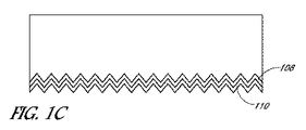
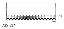
上記シリコン基板の上記受光面上に配置されたトンネル誘電体層を更に備え、上記真性シリコン層は、上記トンネル誘電体層上に配置される、項目1に記載の太陽電池。
(項目4)
上記トンネル誘電体層は、二酸化シリコン(SiO 2 )の層である、項目3に記載の太陽電池。
(項目5)
上記シリコン基板は、単結晶シリコン基板であり、上記真性シリコン層は、真性アモルファスシリコン層であり、上記N型シリコン層は、N型アモルファスシリコン層である、項目4に記載の太陽電池。
(項目6)
上記二酸化シリコン(SiO 2 )の層は、約1〜10ナノメートルの範囲の厚さを有し、上記真性アモルファスシリコン層は、約1〜5ナノメートルの範囲の厚さを有する、項目5に記載の太陽電池。
(項目7)
上記非導電性反射防止コーティング(ARC)層は、窒化シリコンを含む、項目1に記載の太陽電池。
(項目8)
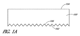
上記受光面は、テクスチャ化されたトポグラフィを有し、上記真性シリコン層は、上記受光面の上記テクスチャ化されたトポグラフィと共形である、項目1に記載の太陽電池。
(項目9)
上記基板は、上記受光面とは反対側の裏面を更に含み、上記太陽電池は、
上記基板の上記裏面、又は上記基板の上記裏面の上方の、複数の互い違いのN型半導体領域及びP型半導体領域と、
上記複数の互い違いのN型半導体領域及びP型半導体領域に結合された導電コンタクト構造体と、
を更に備える、項目1に記載の太陽電池。
(項目10)
受光面を有するシリコン基板と、
上記シリコン基板の上記受光面上に配置されたトンネル誘電体層と、
上記トンネル誘電体層上に配置されたN型シリコン層と、
上記N型シリコン層上に配置された非導電性反射防止コーティング(ARC)層と、
を備える、太陽電池。
(項目11)
上記シリコン基板は、単結晶シリコン基板であり、上記N型シリコン層は、N型アモルファスシリコン層である、項目10に記載の太陽電池。
(項目12)
上記トンネル誘電体層は、約1〜10ナノメートルの範囲の厚さを有する、二酸化シリコン(SiO 2 )の層である、項目10に記載の太陽電池。
(項目13)
上記非導電性反射防止コーティング(ARC)層は、窒化シリコンを含む、項目10に記載の太陽電池。
(項目14)
上記基板の上記受光面は、テクスチャ化されたトポグラフィを有し、上記N型シリコン層は、上記受光面の上記テクスチャ化されたトポグラフィと共形である、項目10に記載の太陽電池。
(項目15)
上記基板は、上記受光面とは反対側の裏面を更に含み、上記太陽電池は、
上記基板の上記裏面、又は上記基板の上記裏面の上方の、複数の互い違いのN型半導体領域及びP型半導体領域と、
上記複数の互い違いのN型半導体領域及びP型半導体領域に結合された導電コンタクト構造体と、
を更に備える、項目10に記載の太陽電池。
(項目16)
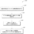
太陽電池を製造する方法であって、
シリコン基板の受光面上にトンネル誘電体層を形成する工程と、
摂氏約300度未満の温度で、上記トンネル誘電体層上にアモルファスシリコン層を形成する工程と、
を備える、方法。
(項目17)
上記トンネル誘電体層を形成する工程は、上記シリコン基板の上記受光面の一部分の化学的酸化、二酸化シリコン(SiO 2 )のプラズマ増強化学気相成長(PECVD)、上記シリコン基板の上記受光面の一部分の熱酸化、及び、O 2 又はO 3 環境中での、紫外線(UV)放射への上記シリコン基板の上記受光面の暴露からなる群から選択される技術を使用する工程を有する、項目16に記載の方法。
(項目18)
上記アモルファスシリコン層を形成する工程は、真性アモルファスシリコン層を形成する工程を有し、上記方法は、
摂氏約300度未満の温度で、上記アモルファスシリコン層上にN型アモルファスシリコン層を形成する工程と、
摂氏約300度未満の温度で、上記N型アモルファスシリコン層上に反射防止コーティング(ARC)層を形成する工程と、
を更に備える、項目16に記載の方法。
(項目19)
上記アモルファスシリコン層を形成する工程は、N型アモルファスシリコン層を形成する工程を有し、上記方法は、
摂氏約300度未満の温度で、上記N型アモルファスシリコン層上に反射防止コーティング(ARC)層を形成する工程を更に備える、項目16に記載の方法。
(項目20)
項目16に記載の方法に従って製造される、太陽電池。
Claims (20)
- 受光面を有するシリコン基板と、
前記シリコン基板の前記受光面の上方に配置された真性シリコン層と、
前記真性シリコン層上に配置されたN型シリコン層と、
前記N型シリコン層上に配置された非導電性反射防止コーティング(ARC)層と、
を備える、太陽電池。 - 前記シリコン基板は、単結晶シリコン基板であり、前記真性シリコン層は、真性アモルファスシリコン層であり、前記N型シリコン層は、N型アモルファスシリコン層である、請求項1に記載の太陽電池。
- 前記シリコン基板の前記受光面上に配置されたトンネル誘電体層を更に備え、前記真性シリコン層は、前記トンネル誘電体層上に配置される、請求項1に記載の太陽電池。
- 前記トンネル誘電体層は、二酸化シリコン(SiO2)の層である、請求項3に記載の太陽電池。
- 前記シリコン基板は、単結晶シリコン基板であり、前記真性シリコン層は、真性アモルファスシリコン層であり、前記N型シリコン層は、N型アモルファスシリコン層である、請求項4に記載の太陽電池。
- 前記二酸化シリコン(SiO2)の層は、約1〜10ナノメートルの範囲の厚さを有し、前記真性アモルファスシリコン層は、約1〜5ナノメートルの範囲の厚さを有する、請求項5に記載の太陽電池。
- 前記非導電性反射防止コーティング(ARC)層は、窒化シリコンを含む、請求項1に記載の太陽電池。
- 前記受光面は、テクスチャ化されたトポグラフィを有し、前記真性シリコン層は、前記受光面の前記テクスチャ化されたトポグラフィと共形である、請求項1に記載の太陽電池。
- 前記基板は、前記受光面とは反対側の裏面を更に含み、前記太陽電池は、
前記基板の前記裏面、又は前記基板の前記裏面の上方の、複数の互い違いのN型半導体領域及びP型半導体領域と、
前記複数の互い違いのN型半導体領域及びP型半導体領域に結合された導電コンタクト構造体と、
を更に備える、請求項1に記載の太陽電池。 - 受光面を有するシリコン基板と、
前記シリコン基板の前記受光面上に配置されたトンネル誘電体層と、
前記トンネル誘電体層上に配置されたN型シリコン層と、
前記N型シリコン層上に配置された非導電性反射防止コーティング(ARC)層と、
を備える、太陽電池。 - 前記シリコン基板は、単結晶シリコン基板であり、前記N型シリコン層は、N型アモルファスシリコン層である、請求項10に記載の太陽電池。
- 前記トンネル誘電体層は、約1〜10ナノメートルの範囲の厚さを有する、二酸化シリコン(SiO2)の層である、請求項10に記載の太陽電池。
- 前記非導電性反射防止コーティング(ARC)層は、窒化シリコンを含む、請求項10に記載の太陽電池。
- 前記基板の前記受光面は、テクスチャ化されたトポグラフィを有し、前記N型シリコン層は、前記受光面の前記テクスチャ化されたトポグラフィと共形である、請求項10に記載の太陽電池。
- 前記基板は、前記受光面とは反対側の裏面を更に含み、前記太陽電池は、
前記基板の前記裏面、又は前記基板の前記裏面の上方の、複数の互い違いのN型半導体領域及びP型半導体領域と、
前記複数の互い違いのN型半導体領域及びP型半導体領域に結合された導電コンタクト構造体と、
を更に備える、請求項10に記載の太陽電池。 - 太陽電池を製造する方法であって、
シリコン基板の受光面上にトンネル誘電体層を形成する工程と、
摂氏約300度未満の温度で、前記トンネル誘電体層上にアモルファスシリコン層を形成する工程と、
を備える、方法。 - 前記トンネル誘電体層を形成する工程は、前記シリコン基板の前記受光面の一部分の化学的酸化、二酸化シリコン(SiO2)のプラズマ増強化学気相成長(PECVD)、前記シリコン基板の前記受光面の一部分の熱酸化、及び、O2又はO3環境中での、紫外線(UV)放射への前記シリコン基板の前記受光面の暴露からなる群から選択される技術を使用する工程を有する、請求項16に記載の方法。
- 前記アモルファスシリコン層を形成する工程は、真性アモルファスシリコン層を形成する工程を有し、前記方法は、
摂氏約300度未満の温度で、前記アモルファスシリコン層上にN型アモルファスシリコン層を形成する工程と、
摂氏約300度未満の温度で、前記N型アモルファスシリコン層上に反射防止コーティング(ARC)層を形成する工程と、
を更に備える、請求項16に記載の方法。 - 前記アモルファスシリコン層を形成する工程は、N型アモルファスシリコン層を形成する工程を有し、前記方法は、
摂氏約300度未満の温度で、前記N型アモルファスシリコン層上に反射防止コーティング(ARC)層を形成する工程を更に備える、請求項16に記載の方法。 - 請求項16に記載の方法に従って製造される、太陽電池。
Applications Claiming Priority (3)
| Application Number | Priority Date | Filing Date | Title |
|---|---|---|---|
| US14/226,368 US20150280018A1 (en) | 2014-03-26 | 2014-03-26 | Passivation of light-receiving surfaces of solar cells |
| US14/226,368 | 2014-03-26 | ||
| PCT/US2015/022331 WO2015148568A1 (en) | 2014-03-26 | 2015-03-24 | Passivation of light-receiving surfaces of solar cells |
Publications (2)
| Publication Number | Publication Date |
|---|---|
| JP2017509153A true JP2017509153A (ja) | 2017-03-30 |
| JP2017509153A5 JP2017509153A5 (ja) | 2018-12-27 |
Family
ID=54191550
Family Applications (1)
| Application Number | Title | Priority Date | Filing Date |
|---|---|---|---|
| JP2016554622A Pending JP2017509153A (ja) | 2014-03-26 | 2015-03-24 | 太陽電池の受光面のパッシベーション |
Country Status (8)
| Country | Link |
|---|---|
| US (2) | US20150280018A1 (ja) |
| JP (1) | JP2017509153A (ja) |
| KR (2) | KR20160138183A (ja) |
| CN (2) | CN106133916B (ja) |
| AU (2) | AU2015236203A1 (ja) |
| DE (1) | DE112015001440T5 (ja) |
| TW (1) | TWI675490B (ja) |
| WO (1) | WO2015148568A1 (ja) |
Families Citing this family (3)
| Publication number | Priority date | Publication date | Assignee | Title |
|---|---|---|---|---|
| US11271129B2 (en) | 2016-11-03 | 2022-03-08 | Total Marketing Services | Surface treatment of solar cells |
| KR101995833B1 (ko) * | 2016-11-14 | 2019-07-03 | 엘지전자 주식회사 | 태양 전지 및 이의 제조 방법 |
| US20190386158A1 (en) * | 2016-12-16 | 2019-12-19 | Sunpower Corporation | Plasma-curing of light-receiving surfaces of solar cells |
Citations (9)
| Publication number | Priority date | Publication date | Assignee | Title |
|---|---|---|---|---|
| JPH06163952A (ja) * | 1992-11-26 | 1994-06-10 | Kyocera Corp | 太陽電池素子 |
| JPH08274356A (ja) * | 1995-03-29 | 1996-10-18 | Kyocera Corp | 太陽電池素子 |
| JPH08298332A (ja) * | 1995-04-26 | 1996-11-12 | Sanyo Electric Co Ltd | 光起電力装置の製造方法 |
| JPH1084125A (ja) * | 1996-07-08 | 1998-03-31 | Semiconductor Energy Lab Co Ltd | 光電変換装置およびその製造方法 |
| JP2003258287A (ja) * | 2002-03-05 | 2003-09-12 | Sanyo Electric Co Ltd | 半導体装置及び光起電力装置並びにその製造方法 |
| JP2010521824A (ja) * | 2007-03-16 | 2010-06-24 | ビーピー・コーポレーション・ノース・アメリカ・インコーポレーテッド | 太陽電池 |
| JP2012501550A (ja) * | 2008-08-27 | 2012-01-19 | アプライド マテリアルズ インコーポレイテッド | 印刷誘電体障壁を使用するバックコンタクト太陽電池 |
| JP2012049156A (ja) * | 2010-08-24 | 2012-03-08 | Osaka Univ | 太陽電池およびその製造方法 |
| CN103346211A (zh) * | 2013-06-26 | 2013-10-09 | 英利集团有限公司 | 一种背接触太阳能电池及其制作方法 |
Family Cites Families (16)
| Publication number | Priority date | Publication date | Assignee | Title |
|---|---|---|---|---|
| US7468485B1 (en) * | 2005-08-11 | 2008-12-23 | Sunpower Corporation | Back side contact solar cell with doped polysilicon regions |
| NL1030200C2 (nl) * | 2005-10-14 | 2007-04-17 | Stichting Energie | Werkwijze voor het vervaardigen van n-type multikristallijn silicium zonnecellen. |
| US20070169808A1 (en) * | 2006-01-26 | 2007-07-26 | Kherani Nazir P | Solar cell |
| US7737357B2 (en) * | 2006-05-04 | 2010-06-15 | Sunpower Corporation | Solar cell having doped semiconductor heterojunction contacts |
| US7960644B2 (en) * | 2007-11-09 | 2011-06-14 | Sunpreme, Ltd. | Low-cost multi-junction solar cells and methods for their production |
| US8076175B2 (en) * | 2008-02-25 | 2011-12-13 | Suniva, Inc. | Method for making solar cell having crystalline silicon P-N homojunction and amorphous silicon heterojunctions for surface passivation |
| WO2011035090A1 (en) * | 2009-09-17 | 2011-03-24 | Tetrasun, Inc. | Selective transformation in functional films, and solar cell applications thereof |
| US20110068367A1 (en) * | 2009-09-23 | 2011-03-24 | Sierra Solar Power, Inc. | Double-sided heterojunction solar cell based on thin epitaxial silicon |
| US8084280B2 (en) * | 2009-10-05 | 2011-12-27 | Akrion Systems, Llc | Method of manufacturing a solar cell using a pre-cleaning step that contributes to homogeneous texture morphology |
| KR20110128619A (ko) * | 2010-05-24 | 2011-11-30 | 삼성전자주식회사 | 태양 전지 및 이의 제조 방법 |
| KR101275575B1 (ko) * | 2010-10-11 | 2013-06-14 | 엘지전자 주식회사 | 후면전극형 태양전지 및 이의 제조 방법 |
| US8492253B2 (en) * | 2010-12-02 | 2013-07-23 | Sunpower Corporation | Method of forming contacts for a back-contact solar cell |
| JP5723143B2 (ja) * | 2010-12-06 | 2015-05-27 | シャープ株式会社 | 裏面電極型太陽電池の製造方法、および裏面電極型太陽電池 |
| JP5879538B2 (ja) * | 2011-03-25 | 2016-03-08 | パナソニックIpマネジメント株式会社 | 光電変換装置及びその製造方法 |
| WO2012132758A1 (ja) * | 2011-03-28 | 2012-10-04 | 三洋電機株式会社 | 光電変換装置及び光電変換装置の製造方法 |
| US20130130430A1 (en) * | 2011-05-20 | 2013-05-23 | Solexel, Inc. | Spatially selective laser annealing applications in high-efficiency solar cells |
-
2014
- 2014-03-26 US US14/226,368 patent/US20150280018A1/en not_active Abandoned
-
2015
- 2015-03-24 JP JP2016554622A patent/JP2017509153A/ja active Pending
- 2015-03-24 WO PCT/US2015/022331 patent/WO2015148568A1/en active Application Filing
- 2015-03-24 KR KR1020167029440A patent/KR20160138183A/ko not_active IP Right Cessation
- 2015-03-24 AU AU2015236203A patent/AU2015236203A1/en not_active Abandoned
- 2015-03-24 KR KR1020217010733A patent/KR20210043013A/ko not_active IP Right Cessation
- 2015-03-24 CN CN201580003357.8A patent/CN106133916B/zh active Active
- 2015-03-24 CN CN201910999294.6A patent/CN110808293A/zh active Pending
- 2015-03-24 DE DE112015001440.3T patent/DE112015001440T5/de not_active Withdrawn
- 2015-03-26 TW TW104109684A patent/TWI675490B/zh active
-
2018
- 2018-10-17 US US16/163,384 patent/US20190051769A1/en not_active Abandoned
-
2019
- 2019-12-18 AU AU2019283886A patent/AU2019283886A1/en not_active Abandoned
Patent Citations (9)
| Publication number | Priority date | Publication date | Assignee | Title |
|---|---|---|---|---|
| JPH06163952A (ja) * | 1992-11-26 | 1994-06-10 | Kyocera Corp | 太陽電池素子 |
| JPH08274356A (ja) * | 1995-03-29 | 1996-10-18 | Kyocera Corp | 太陽電池素子 |
| JPH08298332A (ja) * | 1995-04-26 | 1996-11-12 | Sanyo Electric Co Ltd | 光起電力装置の製造方法 |
| JPH1084125A (ja) * | 1996-07-08 | 1998-03-31 | Semiconductor Energy Lab Co Ltd | 光電変換装置およびその製造方法 |
| JP2003258287A (ja) * | 2002-03-05 | 2003-09-12 | Sanyo Electric Co Ltd | 半導体装置及び光起電力装置並びにその製造方法 |
| JP2010521824A (ja) * | 2007-03-16 | 2010-06-24 | ビーピー・コーポレーション・ノース・アメリカ・インコーポレーテッド | 太陽電池 |
| JP2012501550A (ja) * | 2008-08-27 | 2012-01-19 | アプライド マテリアルズ インコーポレイテッド | 印刷誘電体障壁を使用するバックコンタクト太陽電池 |
| JP2012049156A (ja) * | 2010-08-24 | 2012-03-08 | Osaka Univ | 太陽電池およびその製造方法 |
| CN103346211A (zh) * | 2013-06-26 | 2013-10-09 | 英利集团有限公司 | 一种背接触太阳能电池及其制作方法 |
Also Published As
| Publication number | Publication date |
|---|---|
| TWI675490B (zh) | 2019-10-21 |
| US20190051769A1 (en) | 2019-02-14 |
| CN106133916B (zh) | 2019-11-12 |
| KR20210043013A (ko) | 2021-04-20 |
| DE112015001440T5 (de) | 2017-01-26 |
| TW201611309A (zh) | 2016-03-16 |
| KR20160138183A (ko) | 2016-12-02 |
| WO2015148568A1 (en) | 2015-10-01 |
| AU2015236203A1 (en) | 2016-06-16 |
| CN110808293A (zh) | 2020-02-18 |
| CN106133916A (zh) | 2016-11-16 |
| AU2019283886A1 (en) | 2020-01-23 |
| US20150280018A1 (en) | 2015-10-01 |
Similar Documents
| Publication | Publication Date | Title |
|---|---|---|
| Toor et al. | Efficient nanostructured ‘black’silicon solar cell by copper‐catalyzed metal‐assisted etching | |
| JP6722117B2 (ja) | 結晶シリコンを用いた太陽電池の受光面のパッシベーション | |
| Kulakci et al. | Application of Si nanowires fabricated by metal-assisted etching to crystalline Si solar cells | |
| JP5490231B2 (ja) | 太陽電池素子およびその製造方法ならびに太陽電池モジュール | |
| JP6690859B2 (ja) | 太陽電池内の相対的ドーパント濃度レベル | |
| TWI667798B (zh) | 具無溝槽射極區之太陽能電池 | |
| Es et al. | Metal-assisted nano-textured solar cells with SiO2/Si3N4 passivation | |
| AU2019283886A1 (en) | Passivation of light-receiving surfaces of solar cells | |
| US20140166094A1 (en) | Solar cell emitter region fabrication using etch resistant film | |
| TWI390755B (zh) | 太陽能電池的製造方法 | |
| US20160284917A1 (en) | Passivation Layer for Solar Cells | |
| Hsu et al. | High-efficiency 6′′ multicrystalline black solar cells based on metal-nanoparticle-assisted chemical etching | |
| JP5623131B2 (ja) | 太陽電池素子およびその製造方法ならびに太陽電池モジュール | |
| KR101198438B1 (ko) | 양면 수광형 국부화 에미터 태양전지 및 그 제조 방법 | |
| Baytemir et al. | Radial junction solar cells prepared on single crystalline silicon wafers by metal‐assisted etching | |
| Sepeai et al. | Surface Passivation Studies on n | |
| TWI686958B (zh) | 太陽能電池及其製造方法 | |
| Singh | Fabrication of n+-poly-Si/p+-c-Si tunnel diode using low-pressure chemical vapor deposition for photovoltaic applications | |
| JP6076814B2 (ja) | 太陽電池の製造方法 | |
| CN114613881B (zh) | 太阳能电池及其制备方法、光伏组件 | |
| JP5516611B2 (ja) | 太陽電池の製造方法及び太陽電池 | |
| KR20120077707A (ko) | 국부화 에미터 태양전지 및 그 제조 방법 | |
| Balaji et al. | Laser fired local back contact c-Si solar cells using phosphoric acid for back surface field | |
| Pylypova et al. | Some Advantages of Silicon Nanowires for Photovoltaics Applications | |
| KR20100130044A (ko) | 태양전지의 제조방법 |
Legal Events
| Date | Code | Title | Description |
|---|---|---|---|
| A521 | Request for written amendment filed |
Free format text: JAPANESE INTERMEDIATE CODE: A523 Effective date: 20161026 |
|
| A621 | Written request for application examination |
Free format text: JAPANESE INTERMEDIATE CODE: A621 Effective date: 20180309 |
|
| A521 | Request for written amendment filed |
Free format text: JAPANESE INTERMEDIATE CODE: A523 Effective date: 20181115 |
|
| A977 | Report on retrieval |
Free format text: JAPANESE INTERMEDIATE CODE: A971007 Effective date: 20190129 |
|
| A131 | Notification of reasons for refusal |
Free format text: JAPANESE INTERMEDIATE CODE: A131 Effective date: 20190305 |
|
| A521 | Request for written amendment filed |
Free format text: JAPANESE INTERMEDIATE CODE: A523 Effective date: 20190604 |
|
| A02 | Decision of refusal |
Free format text: JAPANESE INTERMEDIATE CODE: A02 Effective date: 20191126 |
|
| A521 | Request for written amendment filed |
Free format text: JAPANESE INTERMEDIATE CODE: A523 Effective date: 20200326 |
|
| C60 | Trial request (containing other claim documents, opposition documents) |
Free format text: JAPANESE INTERMEDIATE CODE: C60 Effective date: 20200326 |
|
| C11 | Written invitation by the commissioner to file amendments |
Free format text: JAPANESE INTERMEDIATE CODE: C11 Effective date: 20200414 |
|
| A911 | Transfer to examiner for re-examination before appeal (zenchi) |
Free format text: JAPANESE INTERMEDIATE CODE: A911 Effective date: 20200716 |
|
| C21 | Notice of transfer of a case for reconsideration by examiners before appeal proceedings |
Free format text: JAPANESE INTERMEDIATE CODE: C21 Effective date: 20200721 |
|
| A912 | Re-examination (zenchi) completed and case transferred to appeal board |
Free format text: JAPANESE INTERMEDIATE CODE: A912 Effective date: 20200911 |
|
| C211 | Notice of termination of reconsideration by examiners before appeal proceedings |
Free format text: JAPANESE INTERMEDIATE CODE: C211 Effective date: 20200915 |
|
| C22 | Notice of designation (change) of administrative judge |
Free format text: JAPANESE INTERMEDIATE CODE: C22 Effective date: 20201013 |
|
| C141 | Inquiry by the administrative judge |
Free format text: JAPANESE INTERMEDIATE CODE: C141 Effective date: 20201124 |
|
| C54 | Written response to inquiry |
Free format text: JAPANESE INTERMEDIATE CODE: C54 Effective date: 20210125 |
|
| C22 | Notice of designation (change) of administrative judge |
Free format text: JAPANESE INTERMEDIATE CODE: C22 Effective date: 20210406 |
|
| C23 | Notice of termination of proceedings |
Free format text: JAPANESE INTERMEDIATE CODE: C23 Effective date: 20210706 |
|
| C03 | Trial/appeal decision taken |
Free format text: JAPANESE INTERMEDIATE CODE: C03 Effective date: 20210817 |
|
| C30A | Notification sent |
Free format text: JAPANESE INTERMEDIATE CODE: C3012 Effective date: 20210817 |