JP2017183604A - Silicon carbide semiconductor device - Google Patents
Silicon carbide semiconductor device Download PDFInfo
- Publication number
- JP2017183604A JP2017183604A JP2016071217A JP2016071217A JP2017183604A JP 2017183604 A JP2017183604 A JP 2017183604A JP 2016071217 A JP2016071217 A JP 2016071217A JP 2016071217 A JP2016071217 A JP 2016071217A JP 2017183604 A JP2017183604 A JP 2017183604A
- Authority
- JP
- Japan
- Prior art keywords
- silicon carbide
- region
- semiconductor device
- trench
- carbide semiconductor
- Prior art date
- Legal status (The legal status is an assumption and is not a legal conclusion. Google has not performed a legal analysis and makes no representation as to the accuracy of the status listed.)
- Granted
Links
- HBMJWWWQQXIZIP-UHFFFAOYSA-N silicon carbide Chemical compound [Si+]#[C-] HBMJWWWQQXIZIP-UHFFFAOYSA-N 0.000 title claims abstract description 221
- 229910010271 silicon carbide Inorganic materials 0.000 title claims abstract description 220
- 239000004065 semiconductor Substances 0.000 title claims abstract description 99
- 239000000758 substrate Substances 0.000 claims abstract description 22
- 239000012535 impurity Substances 0.000 claims description 127
- 239000013078 crystal Substances 0.000 claims description 5
- 210000000746 body region Anatomy 0.000 abstract description 23
- 230000015556 catabolic process Effects 0.000 abstract description 22
- 230000006378 damage Effects 0.000 abstract description 5
- 238000009413 insulation Methods 0.000 abstract 2
- 239000010410 layer Substances 0.000 description 112
- 230000005684 electric field Effects 0.000 description 14
- 239000011229 interlayer Substances 0.000 description 5
- VYPSYNLAJGMNEJ-UHFFFAOYSA-N Silicium dioxide Chemical compound O=[Si]=O VYPSYNLAJGMNEJ-UHFFFAOYSA-N 0.000 description 4
- 229910052782 aluminium Inorganic materials 0.000 description 4
- XAGFODPZIPBFFR-UHFFFAOYSA-N aluminium Chemical compound [Al] XAGFODPZIPBFFR-UHFFFAOYSA-N 0.000 description 4
- 230000000052 comparative effect Effects 0.000 description 4
- 238000010586 diagram Methods 0.000 description 3
- 239000000463 material Substances 0.000 description 3
- 238000012986 modification Methods 0.000 description 3
- 230000004048 modification Effects 0.000 description 3
- IJGRMHOSHXDMSA-UHFFFAOYSA-N Atomic nitrogen Chemical compound N#N IJGRMHOSHXDMSA-UHFFFAOYSA-N 0.000 description 2
- OAICVXFJPJFONN-UHFFFAOYSA-N Phosphorus Chemical compound [P] OAICVXFJPJFONN-UHFFFAOYSA-N 0.000 description 2
- 229910004298 SiO 2 Inorganic materials 0.000 description 2
- 230000000694 effects Effects 0.000 description 2
- 229910052698 phosphorus Inorganic materials 0.000 description 2
- 239000011574 phosphorus Substances 0.000 description 2
- 235000012239 silicon dioxide Nutrition 0.000 description 2
- 239000000377 silicon dioxide Substances 0.000 description 2
- ZOXJGFHDIHLPTG-UHFFFAOYSA-N Boron Chemical compound [B] ZOXJGFHDIHLPTG-UHFFFAOYSA-N 0.000 description 1
- 238000002441 X-ray diffraction Methods 0.000 description 1
- 229910052796 boron Inorganic materials 0.000 description 1
- 238000011161 development Methods 0.000 description 1
- 238000009792 diffusion process Methods 0.000 description 1
- 230000005669 field effect Effects 0.000 description 1
- 238000007429 general method Methods 0.000 description 1
- 238000005259 measurement Methods 0.000 description 1
- 229910044991 metal oxide Inorganic materials 0.000 description 1
- 150000004706 metal oxides Chemical class 0.000 description 1
- 229910052757 nitrogen Inorganic materials 0.000 description 1
- 230000000149 penetrating effect Effects 0.000 description 1
- 229910021420 polycrystalline silicon Inorganic materials 0.000 description 1
- 229920005591 polysilicon Polymers 0.000 description 1
- 230000002040 relaxant effect Effects 0.000 description 1
Images


Classifications
-
- H—ELECTRICITY
- H01—ELECTRIC ELEMENTS
- H01L—SEMICONDUCTOR DEVICES NOT COVERED BY CLASS H10
- H01L29/00—Semiconductor devices adapted for rectifying, amplifying, oscillating or switching, or capacitors or resistors with at least one potential-jump barrier or surface barrier, e.g. PN junction depletion layer or carrier concentration layer; Details of semiconductor bodies or of electrodes thereof ; Multistep manufacturing processes therefor
- H01L29/02—Semiconductor bodies ; Multistep manufacturing processes therefor
- H01L29/06—Semiconductor bodies ; Multistep manufacturing processes therefor characterised by their shape; characterised by the shapes, relative sizes, or dispositions of the semiconductor regions ; characterised by the concentration or distribution of impurities within semiconductor regions
- H01L29/0603—Semiconductor bodies ; Multistep manufacturing processes therefor characterised by their shape; characterised by the shapes, relative sizes, or dispositions of the semiconductor regions ; characterised by the concentration or distribution of impurities within semiconductor regions characterised by particular constructional design considerations, e.g. for preventing surface leakage, for controlling electric field concentration or for internal isolations regions
- H01L29/0607—Semiconductor bodies ; Multistep manufacturing processes therefor characterised by their shape; characterised by the shapes, relative sizes, or dispositions of the semiconductor regions ; characterised by the concentration or distribution of impurities within semiconductor regions characterised by particular constructional design considerations, e.g. for preventing surface leakage, for controlling electric field concentration or for internal isolations regions for preventing surface leakage or controlling electric field concentration
- H01L29/0611—Semiconductor bodies ; Multistep manufacturing processes therefor characterised by their shape; characterised by the shapes, relative sizes, or dispositions of the semiconductor regions ; characterised by the concentration or distribution of impurities within semiconductor regions characterised by particular constructional design considerations, e.g. for preventing surface leakage, for controlling electric field concentration or for internal isolations regions for preventing surface leakage or controlling electric field concentration for increasing or controlling the breakdown voltage of reverse biased devices
- H01L29/0615—Semiconductor bodies ; Multistep manufacturing processes therefor characterised by their shape; characterised by the shapes, relative sizes, or dispositions of the semiconductor regions ; characterised by the concentration or distribution of impurities within semiconductor regions characterised by particular constructional design considerations, e.g. for preventing surface leakage, for controlling electric field concentration or for internal isolations regions for preventing surface leakage or controlling electric field concentration for increasing or controlling the breakdown voltage of reverse biased devices by the doping profile or the shape or the arrangement of the PN junction, or with supplementary regions, e.g. junction termination extension [JTE]
- H01L29/063—Reduced surface field [RESURF] pn-junction structures
-
- H—ELECTRICITY
- H01—ELECTRIC ELEMENTS
- H01L—SEMICONDUCTOR DEVICES NOT COVERED BY CLASS H10
- H01L29/00—Semiconductor devices adapted for rectifying, amplifying, oscillating or switching, or capacitors or resistors with at least one potential-jump barrier or surface barrier, e.g. PN junction depletion layer or carrier concentration layer; Details of semiconductor bodies or of electrodes thereof ; Multistep manufacturing processes therefor
- H01L29/02—Semiconductor bodies ; Multistep manufacturing processes therefor
- H01L29/06—Semiconductor bodies ; Multistep manufacturing processes therefor characterised by their shape; characterised by the shapes, relative sizes, or dispositions of the semiconductor regions ; characterised by the concentration or distribution of impurities within semiconductor regions
- H01L29/0603—Semiconductor bodies ; Multistep manufacturing processes therefor characterised by their shape; characterised by the shapes, relative sizes, or dispositions of the semiconductor regions ; characterised by the concentration or distribution of impurities within semiconductor regions characterised by particular constructional design considerations, e.g. for preventing surface leakage, for controlling electric field concentration or for internal isolations regions
- H01L29/0607—Semiconductor bodies ; Multistep manufacturing processes therefor characterised by their shape; characterised by the shapes, relative sizes, or dispositions of the semiconductor regions ; characterised by the concentration or distribution of impurities within semiconductor regions characterised by particular constructional design considerations, e.g. for preventing surface leakage, for controlling electric field concentration or for internal isolations regions for preventing surface leakage or controlling electric field concentration
- H01L29/0611—Semiconductor bodies ; Multistep manufacturing processes therefor characterised by their shape; characterised by the shapes, relative sizes, or dispositions of the semiconductor regions ; characterised by the concentration or distribution of impurities within semiconductor regions characterised by particular constructional design considerations, e.g. for preventing surface leakage, for controlling electric field concentration or for internal isolations regions for preventing surface leakage or controlling electric field concentration for increasing or controlling the breakdown voltage of reverse biased devices
- H01L29/0615—Semiconductor bodies ; Multistep manufacturing processes therefor characterised by their shape; characterised by the shapes, relative sizes, or dispositions of the semiconductor regions ; characterised by the concentration or distribution of impurities within semiconductor regions characterised by particular constructional design considerations, e.g. for preventing surface leakage, for controlling electric field concentration or for internal isolations regions for preventing surface leakage or controlling electric field concentration for increasing or controlling the breakdown voltage of reverse biased devices by the doping profile or the shape or the arrangement of the PN junction, or with supplementary regions, e.g. junction termination extension [JTE]
- H01L29/0619—Semiconductor bodies ; Multistep manufacturing processes therefor characterised by their shape; characterised by the shapes, relative sizes, or dispositions of the semiconductor regions ; characterised by the concentration or distribution of impurities within semiconductor regions characterised by particular constructional design considerations, e.g. for preventing surface leakage, for controlling electric field concentration or for internal isolations regions for preventing surface leakage or controlling electric field concentration for increasing or controlling the breakdown voltage of reverse biased devices by the doping profile or the shape or the arrangement of the PN junction, or with supplementary regions, e.g. junction termination extension [JTE] with a supplementary region doped oppositely to or in rectifying contact with the semiconductor containing or contacting region, e.g. guard rings with PN or Schottky junction
- H01L29/0623—Buried supplementary region, e.g. buried guard ring
-
- H—ELECTRICITY
- H01—ELECTRIC ELEMENTS
- H01L—SEMICONDUCTOR DEVICES NOT COVERED BY CLASS H10
- H01L29/00—Semiconductor devices adapted for rectifying, amplifying, oscillating or switching, or capacitors or resistors with at least one potential-jump barrier or surface barrier, e.g. PN junction depletion layer or carrier concentration layer; Details of semiconductor bodies or of electrodes thereof ; Multistep manufacturing processes therefor
- H01L29/02—Semiconductor bodies ; Multistep manufacturing processes therefor
- H01L29/06—Semiconductor bodies ; Multistep manufacturing processes therefor characterised by their shape; characterised by the shapes, relative sizes, or dispositions of the semiconductor regions ; characterised by the concentration or distribution of impurities within semiconductor regions
- H01L29/08—Semiconductor bodies ; Multistep manufacturing processes therefor characterised by their shape; characterised by the shapes, relative sizes, or dispositions of the semiconductor regions ; characterised by the concentration or distribution of impurities within semiconductor regions with semiconductor regions connected to an electrode carrying current to be rectified, amplified or switched and such electrode being part of a semiconductor device which comprises three or more electrodes
- H01L29/0843—Source or drain regions of field-effect devices
- H01L29/0847—Source or drain regions of field-effect devices of field-effect transistors with insulated gate
- H01L29/0852—Source or drain regions of field-effect devices of field-effect transistors with insulated gate of DMOS transistors
- H01L29/0873—Drain regions
- H01L29/0878—Impurity concentration or distribution
-
- H—ELECTRICITY
- H01—ELECTRIC ELEMENTS
- H01L—SEMICONDUCTOR DEVICES NOT COVERED BY CLASS H10
- H01L29/00—Semiconductor devices adapted for rectifying, amplifying, oscillating or switching, or capacitors or resistors with at least one potential-jump barrier or surface barrier, e.g. PN junction depletion layer or carrier concentration layer; Details of semiconductor bodies or of electrodes thereof ; Multistep manufacturing processes therefor
- H01L29/02—Semiconductor bodies ; Multistep manufacturing processes therefor
- H01L29/06—Semiconductor bodies ; Multistep manufacturing processes therefor characterised by their shape; characterised by the shapes, relative sizes, or dispositions of the semiconductor regions ; characterised by the concentration or distribution of impurities within semiconductor regions
- H01L29/10—Semiconductor bodies ; Multistep manufacturing processes therefor characterised by their shape; characterised by the shapes, relative sizes, or dispositions of the semiconductor regions ; characterised by the concentration or distribution of impurities within semiconductor regions with semiconductor regions connected to an electrode not carrying current to be rectified, amplified or switched and such electrode being part of a semiconductor device which comprises three or more electrodes
- H01L29/1095—Body region, i.e. base region, of DMOS transistors or IGBTs
-
- H—ELECTRICITY
- H01—ELECTRIC ELEMENTS
- H01L—SEMICONDUCTOR DEVICES NOT COVERED BY CLASS H10
- H01L29/00—Semiconductor devices adapted for rectifying, amplifying, oscillating or switching, or capacitors or resistors with at least one potential-jump barrier or surface barrier, e.g. PN junction depletion layer or carrier concentration layer; Details of semiconductor bodies or of electrodes thereof ; Multistep manufacturing processes therefor
- H01L29/02—Semiconductor bodies ; Multistep manufacturing processes therefor
- H01L29/12—Semiconductor bodies ; Multistep manufacturing processes therefor characterised by the materials of which they are formed
- H01L29/16—Semiconductor bodies ; Multistep manufacturing processes therefor characterised by the materials of which they are formed including, apart from doping materials or other impurities, only elements of Group IV of the Periodic System
- H01L29/1608—Silicon carbide
-
- H—ELECTRICITY
- H01—ELECTRIC ELEMENTS
- H01L—SEMICONDUCTOR DEVICES NOT COVERED BY CLASS H10
- H01L29/00—Semiconductor devices adapted for rectifying, amplifying, oscillating or switching, or capacitors or resistors with at least one potential-jump barrier or surface barrier, e.g. PN junction depletion layer or carrier concentration layer; Details of semiconductor bodies or of electrodes thereof ; Multistep manufacturing processes therefor
- H01L29/40—Electrodes ; Multistep manufacturing processes therefor
- H01L29/41—Electrodes ; Multistep manufacturing processes therefor characterised by their shape, relative sizes or dispositions
- H01L29/423—Electrodes ; Multistep manufacturing processes therefor characterised by their shape, relative sizes or dispositions not carrying the current to be rectified, amplified or switched
- H01L29/42312—Gate electrodes for field effect devices
- H01L29/42316—Gate electrodes for field effect devices for field-effect transistors
- H01L29/4232—Gate electrodes for field effect devices for field-effect transistors with insulated gate
- H01L29/42356—Disposition, e.g. buried gate electrode
- H01L29/4236—Disposition, e.g. buried gate electrode within a trench, e.g. trench gate electrode, groove gate electrode
-
- H—ELECTRICITY
- H01—ELECTRIC ELEMENTS
- H01L—SEMICONDUCTOR DEVICES NOT COVERED BY CLASS H10
- H01L29/00—Semiconductor devices adapted for rectifying, amplifying, oscillating or switching, or capacitors or resistors with at least one potential-jump barrier or surface barrier, e.g. PN junction depletion layer or carrier concentration layer; Details of semiconductor bodies or of electrodes thereof ; Multistep manufacturing processes therefor
- H01L29/40—Electrodes ; Multistep manufacturing processes therefor
- H01L29/41—Electrodes ; Multistep manufacturing processes therefor characterised by their shape, relative sizes or dispositions
- H01L29/423—Electrodes ; Multistep manufacturing processes therefor characterised by their shape, relative sizes or dispositions not carrying the current to be rectified, amplified or switched
- H01L29/42312—Gate electrodes for field effect devices
- H01L29/42316—Gate electrodes for field effect devices for field-effect transistors
- H01L29/4232—Gate electrodes for field effect devices for field-effect transistors with insulated gate
- H01L29/42364—Gate electrodes for field effect devices for field-effect transistors with insulated gate characterised by the insulating layer, e.g. thickness or uniformity
- H01L29/42368—Gate electrodes for field effect devices for field-effect transistors with insulated gate characterised by the insulating layer, e.g. thickness or uniformity the thickness being non-uniform
-
- H—ELECTRICITY
- H01—ELECTRIC ELEMENTS
- H01L—SEMICONDUCTOR DEVICES NOT COVERED BY CLASS H10
- H01L29/00—Semiconductor devices adapted for rectifying, amplifying, oscillating or switching, or capacitors or resistors with at least one potential-jump barrier or surface barrier, e.g. PN junction depletion layer or carrier concentration layer; Details of semiconductor bodies or of electrodes thereof ; Multistep manufacturing processes therefor
- H01L29/66—Types of semiconductor device ; Multistep manufacturing processes therefor
- H01L29/68—Types of semiconductor device ; Multistep manufacturing processes therefor controllable by only the electric current supplied, or only the electric potential applied, to an electrode which does not carry the current to be rectified, amplified or switched
- H01L29/70—Bipolar devices
- H01L29/72—Transistor-type devices, i.e. able to continuously respond to applied control signals
- H01L29/739—Transistor-type devices, i.e. able to continuously respond to applied control signals controlled by field-effect, e.g. bipolar static induction transistors [BSIT]
- H01L29/7393—Insulated gate bipolar mode transistors, i.e. IGBT; IGT; COMFET
- H01L29/7395—Vertical transistors, e.g. vertical IGBT
- H01L29/7396—Vertical transistors, e.g. vertical IGBT with a non planar surface, e.g. with a non planar gate or with a trench or recess or pillar in the surface of the emitter, base or collector region for improving current density or short circuiting the emitter and base regions
- H01L29/7397—Vertical transistors, e.g. vertical IGBT with a non planar surface, e.g. with a non planar gate or with a trench or recess or pillar in the surface of the emitter, base or collector region for improving current density or short circuiting the emitter and base regions and a gate structure lying on a slanted or vertical surface or formed in a groove, e.g. trench gate IGBT
-
- H—ELECTRICITY
- H01—ELECTRIC ELEMENTS
- H01L—SEMICONDUCTOR DEVICES NOT COVERED BY CLASS H10
- H01L29/00—Semiconductor devices adapted for rectifying, amplifying, oscillating or switching, or capacitors or resistors with at least one potential-jump barrier or surface barrier, e.g. PN junction depletion layer or carrier concentration layer; Details of semiconductor bodies or of electrodes thereof ; Multistep manufacturing processes therefor
- H01L29/66—Types of semiconductor device ; Multistep manufacturing processes therefor
- H01L29/68—Types of semiconductor device ; Multistep manufacturing processes therefor controllable by only the electric current supplied, or only the electric potential applied, to an electrode which does not carry the current to be rectified, amplified or switched
- H01L29/76—Unipolar devices, e.g. field effect transistors
- H01L29/772—Field effect transistors
- H01L29/78—Field effect transistors with field effect produced by an insulated gate
- H01L29/7801—DMOS transistors, i.e. MISFETs with a channel accommodating body or base region adjoining a drain drift region
- H01L29/7802—Vertical DMOS transistors, i.e. VDMOS transistors
- H01L29/7813—Vertical DMOS transistors, i.e. VDMOS transistors with trench gate electrode, e.g. UMOS transistors
-
- H—ELECTRICITY
- H01—ELECTRIC ELEMENTS
- H01L—SEMICONDUCTOR DEVICES NOT COVERED BY CLASS H10
- H01L29/00—Semiconductor devices adapted for rectifying, amplifying, oscillating or switching, or capacitors or resistors with at least one potential-jump barrier or surface barrier, e.g. PN junction depletion layer or carrier concentration layer; Details of semiconductor bodies or of electrodes thereof ; Multistep manufacturing processes therefor
- H01L29/40—Electrodes ; Multistep manufacturing processes therefor
- H01L29/41—Electrodes ; Multistep manufacturing processes therefor characterised by their shape, relative sizes or dispositions
- H01L29/423—Electrodes ; Multistep manufacturing processes therefor characterised by their shape, relative sizes or dispositions not carrying the current to be rectified, amplified or switched
- H01L29/42312—Gate electrodes for field effect devices
- H01L29/42316—Gate electrodes for field effect devices for field-effect transistors
- H01L29/4232—Gate electrodes for field effect devices for field-effect transistors with insulated gate
- H01L29/42372—Gate electrodes for field effect devices for field-effect transistors with insulated gate characterised by the conducting layer, e.g. the length, the sectional shape or the lay-out
- H01L29/42376—Gate electrodes for field effect devices for field-effect transistors with insulated gate characterised by the conducting layer, e.g. the length, the sectional shape or the lay-out characterised by the length or the sectional shape
Abstract
Description
本発明は、炭化珪素半導体装置に関する。 The present invention relates to a silicon carbide semiconductor device.
近年、半導体装置の高耐圧化、低損失化、高温環境下での使用などを可能とするため、半導体装置を構成する材料として炭化珪素(SiC)の採用が進められつつある。 In recent years, silicon carbide (SiC) has been increasingly adopted as a material constituting semiconductor devices in order to enable higher breakdown voltage, lower loss, and use in high-temperature environments.
オン抵抗の低減にとって有利であるという観点から、炭化珪素半導体装置の分野において、トレンチゲートを有するMOSFET(Metal Oxide Semiconductor Field Effect Transistor)またはトレンチゲートを有するIGBT(Insulated Gate Bipolar Transistor)の開発が進められている。トレンチゲートを有する炭化珪素半導体装置においては、トレンチ構造の底部においてゲート絶縁膜の絶縁破壊が生じやすいという課題が存在する。 In the field of silicon carbide semiconductor devices, the development of MOSFETs (Metal Oxide Semiconductor Field Effect Transistors) having trench gates or IGBTs (Insulated Gate Bipolar Transistors) having trench gates has been promoted in the field of silicon carbide semiconductor devices from the viewpoint of being advantageous for reducing on-resistance. ing. In a silicon carbide semiconductor device having a trench gate, there is a problem that dielectric breakdown of the gate insulating film easily occurs at the bottom of the trench structure.
このような課題を解決するための様々な構造が提案されている。たとえば国際公開2012/077617号(特許文献1)、特開2012−99601号公報(特許文献2)および特開2013−69964号公報(特許文献3)は、トレンチの下部に形成されたp型拡散層を含む炭化珪素半導体装置を開示する。 Various structures for solving such a problem have been proposed. For example, International Publication No. 2012/077617 (Patent Document 1), Japanese Unexamined Patent Application Publication No. 2012-99601 (Patent Document 2), and Japanese Unexamined Patent Application Publication No. 2013-69964 (Patent Document 3) describe p-type diffusion formed in a lower portion of a trench. A silicon carbide semiconductor device including a layer is disclosed.
特開2013−145770号公報(特許文献4)は、ソース領域に形成された深いp型領域を有する炭化珪素半導体装置を開示する。特開2014−41990号公報(特許文献5)は、埋め込まれたp型領域を有する炭化珪素半導体装置を開示する。 Japanese Patent Laying-Open No. 2013-145770 (Patent Document 4) discloses a silicon carbide semiconductor device having a deep p-type region formed in a source region. Japanese Patent Laying-Open No. 2014-41990 (Patent Document 5) discloses a silicon carbide semiconductor device having a buried p-type region.
特許文献1〜3に開示された炭化珪素半導体装置においては、p型領域がトレンチの底部に配置される。しかし、このような構造においては、狭窄抵抗が、そのp型領域と、p型のボディ領域との間に生じやすい。狭窄抵抗の抵抗値が高いことによって、炭化珪素半導体装置のオン抵抗の増大をもたらす。
In the silicon carbide semiconductor devices disclosed in
また、そのp型領域においてアバランシェブレークダウンが生じた場合には、ゲート絶縁膜を貫通してトレンチゲートに大電流が流れる可能性がある。すなわち、アバランシェブレークダウンによって、ゲート絶縁膜が損傷する可能性がある。 When an avalanche breakdown occurs in the p-type region, a large current may flow through the gate insulating film to the trench gate. That is, the gate insulating film may be damaged by the avalanche breakdown.
本発明の目的は、オン抵抗の増加を招くことなく、アバランシェブレークダウンの発生時におけるゲート絶縁膜の損傷の可能性を低くすることができる炭化珪素半導体装置を提供することである。 An object of the present invention is to provide a silicon carbide semiconductor device that can reduce the possibility of damage to a gate insulating film when an avalanche breakdown occurs without causing an increase in on-resistance.
本発明の一態様に係る炭化珪素半導体装置は、炭化珪素基板と、第1の炭化珪素層と、第2の炭化珪素層と、第3の炭化珪素層と、第4の炭化珪素層と、第1の不純物領域とを備える。第1の炭化珪素層は、炭化珪素基板上に配置され、第1の導電型を有する。第2の炭化珪素層は、第1の炭化珪素層上に配置され、第1の導電型を有する。第3の炭化珪素層は、第2の炭化珪素層上に配置され、第1の導電型と異なる第2の導電型を有する。第4の炭化珪素層は、第3の炭化珪素層上に配置され、第1の導電型を有する。第1の不純物領域は、第2の炭化珪素層、第3の炭化珪素層および第4の炭化珪素層を貫通するように形成され、第2の導電型を有する。トレンチが、第4の炭化珪素層から第3の炭化珪素層を貫通して第2の炭化珪素層に達するように、炭化珪素半導体装置に形成される。炭化珪素半導体装置は、トレンチの壁に接触したゲート絶縁膜と、ゲート電極と、第2の不純物領域と、第3の不純物領域と、第4の不純物領域とを備える。ゲート電極は、ゲート絶縁膜に接触し、かつ、トレンチに充填される。第2の不純物領域は、トレンチの下方にトレンチの底部から離間して配置され、第2の導電型を有する。第3の不純物領域は、第1の不純物領域に接するように第1の不純物領域の下方に形成され、第2の導電型を有し、かつ、第2の不純物領域に電気的に接続される。第4の不純物領域は、第2の不純物領域と第3の不純物領域との間に形成され、第1の導電型を有する。 A silicon carbide semiconductor device according to one embodiment of the present invention includes a silicon carbide substrate, a first silicon carbide layer, a second silicon carbide layer, a third silicon carbide layer, a fourth silicon carbide layer, A first impurity region. The first silicon carbide layer is disposed on the silicon carbide substrate and has the first conductivity type. The second silicon carbide layer is disposed on the first silicon carbide layer and has the first conductivity type. The third silicon carbide layer is disposed on the second silicon carbide layer and has a second conductivity type different from the first conductivity type. The fourth silicon carbide layer is disposed on the third silicon carbide layer and has the first conductivity type. The first impurity region is formed to penetrate through the second silicon carbide layer, the third silicon carbide layer, and the fourth silicon carbide layer, and has the second conductivity type. A trench is formed in the silicon carbide semiconductor device so as to reach the second silicon carbide layer from the fourth silicon carbide layer through the third silicon carbide layer. The silicon carbide semiconductor device includes a gate insulating film in contact with a trench wall, a gate electrode, a second impurity region, a third impurity region, and a fourth impurity region. The gate electrode contacts the gate insulating film and fills the trench. The second impurity region is disposed below the trench and spaced from the bottom of the trench, and has the second conductivity type. The third impurity region is formed below the first impurity region so as to be in contact with the first impurity region, has the second conductivity type, and is electrically connected to the second impurity region. . The fourth impurity region is formed between the second impurity region and the third impurity region, and has the first conductivity type.
上記によれば、オン抵抗の増加を招くことなく、アバランシェブレークダウン時におけるゲート絶縁膜の破壊の可能性を低くすることができる炭化珪素半導体装置を実現できる。 According to the above, a silicon carbide semiconductor device that can reduce the possibility of destruction of the gate insulating film during avalanche breakdown without increasing the on-resistance can be realized.
[本発明の実施形態の説明]
以下、図面を参照しつつ、本発明の実施の形態について説明する。以下の説明では、同一または対応する要素には同一の符号を付して、それらについての詳細な説明は繰り返さない。
[Description of Embodiment of the Present Invention]
Hereinafter, embodiments of the present invention will be described with reference to the drawings. In the following description, the same or corresponding elements are denoted by the same reference numerals, and detailed description thereof will not be repeated.
本明細書中の結晶学的記載においては、個別方位を[]、集合方位を<>、個別面を()、集合面を{}でそれぞれ示している。結晶学上の指数が負であることは、通常、”−”(バー)を数字の上に付すことによって表現されるが、本明細書中では数字の前に負の符号を付すことで結晶学上の負の指数が表現される。また角度の記載には、全方位角を360度とする系を用いている。 In the crystallographic description in this specification, the individual orientation is indicated by [], the collective orientation is indicated by <>, the individual plane is indicated by (), and the collective plane is indicated by {}. A negative crystallographic index is usually expressed by adding a “-” (bar) above a number, but in this specification a crystal is obtained by adding a negative sign before the number. A negative academic exponent is expressed. The angle is described using a system in which the omnidirectional angle is 360 degrees.
最初に本発明の実施態様を列記して説明する。
(1)本発明の一態様に係る炭化珪素半導体装置(1)は、炭化珪素基板(10)と、第1の炭化珪素層(11)と、第2の炭化珪素層(13)と、第3の炭化珪素層(14)と、第4の炭化珪素層(15)と、第1の不純物領域(16)とを備える。第1の炭化珪素層(11)は、炭化珪素基板(10)上に配置され、第1の導電型を有する。第2の炭化珪素層(13)は、第1の炭化珪素層(11)上に配置され、第1の導電型を有する。第3の炭化珪素層(14)は、第2の炭化珪素層(13)上に配置され、第1の導電型と異なる第2の導電型を有する。第4の炭化珪素層(15)は、第3の炭化珪素層(14)上に配置され、第1の導電型を有する。第1の不純物領域(16)は、第2の炭化珪素層(13)、第3の炭化珪素層(14)および第4の炭化珪素層(15)を貫通するように形成され、第2の導電型を有する。トレンチ(21)が、第4の炭化珪素層(15)から第3の炭化珪素層(14)を貫通して第2の炭化珪素層(13)に達するように、炭化珪素半導体装置(1)に形成される。炭化珪素半導体装置(1)は、トレンチ(21)の壁に接触したゲート絶縁膜(25)と、ゲート電極(30)と、第2の不純物領域(17)と、第3の不純物領域(18)と、第4の不純物領域(20)とを備える。ゲート電極(30)は、ゲート絶縁膜(25)に接触し、かつ、トレンチ(21)に充填される。第2の不純物領域(17)は、トレンチ(21)の下方にトレンチ(21)の底部から離間して配置され、第2の導電型を有する。第3の不純物領域(18)は、第1の不純物領域(16)に接するように第1の不純物領域(16)の下方に形成され、第2の導電型を有し、かつ、第2の不純物領域(17)に電気的に接続される。第4の不純物領域(20)は、第2の不純物領域(17)と第3の不純物領域(18)との間に形成され、第1の導電型を有する。
First, embodiments of the present invention will be listed and described.
(1) A silicon carbide semiconductor device (1) according to one embodiment of the present invention includes a silicon carbide substrate (10), a first silicon carbide layer (11), a second silicon carbide layer (13), 3 silicon carbide layer (14), a fourth silicon carbide layer (15), and a first impurity region (16). The first silicon carbide layer (11) is disposed on the silicon carbide substrate (10) and has the first conductivity type. The second silicon carbide layer (13) is disposed on the first silicon carbide layer (11) and has the first conductivity type. The third silicon carbide layer (14) is disposed on the second silicon carbide layer (13) and has a second conductivity type different from the first conductivity type. The fourth silicon carbide layer (15) is disposed on the third silicon carbide layer (14) and has the first conductivity type. The first impurity region (16) is formed so as to penetrate the second silicon carbide layer (13), the third silicon carbide layer (14), and the fourth silicon carbide layer (15). Has conductivity type. The silicon carbide semiconductor device (1) so that the trench (21) penetrates the third silicon carbide layer (14) from the fourth silicon carbide layer (15) to the second silicon carbide layer (13). Formed. The silicon carbide semiconductor device (1) includes a gate insulating film (25) in contact with the wall of the trench (21), a gate electrode (30), a second impurity region (17), and a third impurity region (18). ) And a fourth impurity region (20). The gate electrode (30) contacts the gate insulating film (25) and fills the trench (21). The second impurity region (17) is disposed below the trench (21) and spaced from the bottom of the trench (21), and has the second conductivity type. The third impurity region (18) is formed below the first impurity region (16) so as to be in contact with the first impurity region (16), has a second conductivity type, and has a second conductivity type. It is electrically connected to the impurity region (17). The fourth impurity region (20) is formed between the second impurity region (17) and the third impurity region (18), and has the first conductivity type.
上記によれば、オン抵抗の増加を招くことなく、アバランシェブレークダウン時におけるゲート絶縁膜の破壊の可能性を低くすることができる炭化珪素半導体装置を実現できる。第2の不純物領域が、トレンチの下方にトレンチの底部から離間して配置される。したがって、狭窄抵抗によるオン抵抗の増大を抑えることができる。さらに、アバランシェブレークダウンが発生した際にも、ゲート絶縁膜を貫通する電流が生じる可能性を小さくすることができる。したがって、ゲート絶縁膜の破壊の可能性を低くすることができる。 According to the above, a silicon carbide semiconductor device that can reduce the possibility of destruction of the gate insulating film during avalanche breakdown without increasing the on-resistance can be realized. A second impurity region is disposed below the trench and spaced from the bottom of the trench. Therefore, an increase in on-resistance due to constriction resistance can be suppressed. Furthermore, even when an avalanche breakdown occurs, the possibility that a current passing through the gate insulating film is generated can be reduced. Therefore, the possibility of destruction of the gate insulating film can be reduced.
(2)上記(1)の炭化珪素半導体装置において、第2の炭化珪素層(13)の不純物濃度(ND2)は、第1の炭化珪素層(11)の不純物濃度(ND1)よりも大きい。第4の不純物領域(20)の不純物濃度(NJ)は、第2の炭化珪素層(13)の不純物濃度(ND2)よりも大きい。第2の不純物領域(17)の不純物濃度(NBP)は、第4の不純物領域(20)の不純物濃度(NJ)よりも大きい。 (2) In the silicon carbide semiconductor device of (1), the impurity concentration (N D2 ) of the second silicon carbide layer (13) is higher than the impurity concentration (N D1 ) of the first silicon carbide layer (11). large. The impurity concentration (N J ) of the fourth impurity region (20) is higher than the impurity concentration (N D2 ) of the second silicon carbide layer (13). The impurity concentration (N BP ) of the second impurity region (17) is higher than the impurity concentration (N J ) of the fourth impurity region (20).
第2の炭化珪素層の不純物濃度が第1の炭化珪素層の不純物濃度よりも大きいことにより、炭化珪素半導体装置のオン抵抗を下げることができる。さらに、第4の不純物領域の不純物濃度が第2の炭化珪素層の不純物濃度よりも大きいことにより、炭化珪素半導体装置のオン抵抗を下げることができる。一方で、第2の不純物領域の不純物濃度は、第4の不純物領域の不純物濃度よりも大きい。これにより、これにより所定の大きさの逆バイアス電圧が炭化珪素半導体装置にドレイン電極に印加された場合にも、第2の不純物領域が完全に空乏化しにくくなる。ゲート絶縁膜に印加される電界を緩和することができるので、ゲート絶縁膜が破壊する可能性を小さくすることができる。 When the impurity concentration of the second silicon carbide layer is higher than the impurity concentration of the first silicon carbide layer, the on-resistance of the silicon carbide semiconductor device can be lowered. Furthermore, the on-resistance of the silicon carbide semiconductor device can be lowered because the impurity concentration of the fourth impurity region is higher than the impurity concentration of the second silicon carbide layer. On the other hand, the impurity concentration of the second impurity region is higher than the impurity concentration of the fourth impurity region. Thereby, even when a reverse bias voltage of a predetermined magnitude is applied to the drain electrode of the silicon carbide semiconductor device, the second impurity region is not easily depleted. Since the electric field applied to the gate insulating film can be relaxed, the possibility that the gate insulating film is broken can be reduced.
(3)上記(1)または(2)の炭化珪素半導体装置において、第1の炭化珪素層(11)と第2の炭化珪素層(13)との界面(11A)からの第4の不純物領域(20)の深さ(DJ)は、その界面(11A)からの第2の不純物領域(17)の深さ(DBP)よりも小さい。 (3) In the silicon carbide semiconductor device of (1) or (2), a fourth impurity region from the interface (11A) between the first silicon carbide layer (11) and the second silicon carbide layer (13) The depth (D J ) of (20) is smaller than the depth (D BP ) of the second impurity region (17) from the interface (11A).
上記によれば、炭化珪素半導体装置のオン抵抗が上昇することを抑えることができる。
(4)上記(1)から(3)のいずれかの炭化珪素半導体装置において、トレンチ(21)の底部(21B)から第2の不純物領域(17)までの距離をD1と表すと、0.1μm≦D1≦3.0μmの関係が成り立つ。
According to the above, it is possible to suppress an increase in the on-resistance of the silicon carbide semiconductor device.
In any of the silicon carbide semiconductor device (4) from above (1) (3), the distance of the bottom of the trench (21) from (21B) to the second impurity region (17) is represented as D 1, 0 The relationship of 1 μm ≦ D 1 ≦ 3.0 μm is established.
上記によれば、オン抵抗の増大を抑えることができるとともに、アバランシェブレークダウンが生じた際にゲート絶縁膜が破壊する可能性を小さくすることができる。 According to the above, it is possible to suppress an increase in on-resistance and to reduce the possibility that the gate insulating film breaks when an avalanche breakdown occurs.
(5)上記(1)から(4)のいずれかの炭化珪素半導体装置において、第3の不純物領域(18)の横方向の幅(WBP1)は、第2の不純物領域(17)の横方向の幅(WBP2)よりも小さい。 (5) In the silicon carbide semiconductor device according to any one of (1) to (4), the lateral width (W BP1 ) of the third impurity region (18) is equal to the lateral width of the second impurity region (17). It is smaller than the width in the direction (W BP2 ).
上記によれば、第2の不純物領域に比べて第3の不純物領域のほうがアバランシェブレークダウンが生じやすい。したがってアバランシェブレークダウンが生じた際にゲート絶縁膜が破壊する可能性を小さくすることができる。 According to the above, an avalanche breakdown is more likely to occur in the third impurity region than in the second impurity region. Therefore, the possibility that the gate insulating film breaks when avalanche breakdown occurs can be reduced.
(6)上記(1)から(5)のいずれかの炭化珪素半導体装置において、第2の不純物領域(17)の横方向の幅(WBP2)は、トレンチ(21)の横方向の幅(Wtrench)よりも大きい。 (6) In the silicon carbide semiconductor device according to any one of (1) to (5), the lateral width (W BP2 ) of the second impurity region (17) is the lateral width of the trench (21) ( W trench ).
上記によれば、第2の不純物領域から広がる空乏層の横方向の幅を、トレンチの横方向の幅よりも大きくすることができる。したがって、トレンチの底部において、ゲート絶縁膜に印加される電界を低減することができる。 According to the above, the lateral width of the depletion layer extending from the second impurity region can be made larger than the lateral width of the trench. Therefore, the electric field applied to the gate insulating film at the bottom of the trench can be reduced.
(7)上記(1)から(6)のいずれかの炭化珪素半導体装置において、トレンチ(21)の底部におけるゲート絶縁膜(25)の厚さ(tg1)は、トレンチ(21)の側壁に接するゲート絶縁膜(25)の部分の厚さ(tg2)よりも大きい。 (7) In the silicon carbide semiconductor device according to any one of (1) to (6), the thickness (t g1 ) of the gate insulating film (25) at the bottom of the trench (21) is on the side wall of the trench (21). It is larger than the thickness (t g2 ) of the portion of the gate insulating film (25) in contact therewith .
上記によれば、トレンチの底部においてアバランシェブレークダウンが生じた場合にも、ゲート絶縁膜が破壊する可能性を小さくすることができる。 According to the above, even when an avalanche breakdown occurs at the bottom of the trench, the possibility that the gate insulating film is broken can be reduced.
(8)上記(1)から(7)のいずれかの炭化珪素半導体装置において、トレンチ(21)の側壁(21A)の結晶面方位が<1−100>または<11−20>である。 (8) In the silicon carbide semiconductor device according to any one of (1) to (7), the crystal plane orientation of the side wall (21A) of the trench (21) is <1-100> or <11-20>.
上記によれば、炭化珪素半導体装置のオン抵抗を小さくすることができる。
(9)上記(1)から(8)のいずれかの炭化珪素半導体装置において、トレンチ(21)は、{0001}面に対して傾斜した側壁面(21A)を有する。
According to the above, the on-resistance of the silicon carbide semiconductor device can be reduced.
(9) In the silicon carbide semiconductor device according to any one of (1) to (8), the trench (21) has a side wall surface (21A) inclined with respect to the {0001} plane.
上記によれば、炭化珪素半導体装置のオン抵抗を小さくすることができる。
(10)上記(1)から(9)のいずれかの炭化珪素半導体装置は、MOSFETである。炭化珪素基板(10)は、第1の導電型を有する。
According to the above, the on-resistance of the silicon carbide semiconductor device can be reduced.
(10) The silicon carbide semiconductor device according to any one of (1) to (9) is a MOSFET. The silicon carbide substrate (10) has the first conductivity type.
上記によれば、炭化珪素半導体装置によって、トレンチゲートを有するMOSFETを実現できる。 According to the above, a MOSFET having a trench gate can be realized by the silicon carbide semiconductor device.
(11)上記(1)から(9)のいずれかの炭化珪素半導体装置は、IGBTである。炭化珪素基板(10)は、第2の導電型を有する。 (11) The silicon carbide semiconductor device according to any one of (1) to (9) is an IGBT. The silicon carbide substrate (10) has the second conductivity type.
上記によれば、炭化珪素半導体装置によって、トレンチゲートを有するIGBTを実現できる。 According to the above, an IGBT having a trench gate can be realized by the silicon carbide semiconductor device.
[本発明の実施形態の詳細]
本発明の実施の形態に係る炭化珪素半導体装置の一例として、MOSFETが以下に例示される。
[Details of the embodiment of the present invention]
MOSFET is illustrated below as an example of the silicon carbide semiconductor device which concerns on embodiment of this invention.
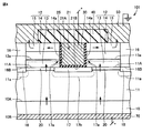
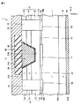
図1は、本発明の一実施形態に係る炭化珪素半導体装置の構造を示した断面図である。図1を参照して、炭化珪素半導体装置1は、炭化珪素基板10と、炭化珪素エピタキシャル層11,12と、ゲート絶縁膜25と、ゲート電極30と、層間絶縁膜40と、ソース電極50と、ドレイン電極70とを含む。
FIG. 1 is a cross-sectional view showing a structure of a silicon carbide semiconductor device according to an embodiment of the present invention. Referring to FIG. 1, silicon
炭化珪素基板10は、主面10A,10Bを有する。主面10A,10Bは互いに反対の側に位置する。炭化珪素エピタキシャル層11(第1の炭化珪素層)は、主面10A上に配置される。炭化珪素エピタキシャル層12は、炭化珪素エピタキシャル層11上に配置される。
炭化珪素基板10、および炭化珪素エピタキシャル層11,12は、第1の導電型を有する。この実施の形態では、第1の導電型はn型である。炭化珪素基板10、および炭化珪素エピタキシャル層11,12は、たとえばN(窒素)などのn型不純物を含む。
炭化珪素エピタキシャル層12は、ドリフト領域13、ボディ領域14、ソース領域15およびディープ領域16(第1の不純物領域)を含む。ドリフト領域13、ボディ領域14、ソース領域15は、層状に形成される。すなわち、ドリフト領域13、ボディ領域14、ソース領域15は、それぞれ、第2の炭化珪素層、第3の炭化珪素層、および第4の炭化珪素層に相当する。
Silicon
ドリフト領域13の導電型はn型である。ドリフト領域13の不純物濃度は、炭化珪素エピタキシャル層12の不純物濃度に実質的に等しい。
The conductivity type of
ボディ領域14は、ドリフト領域13上に形成される。ボディ領域14は、第1の導電型と異なる第2の導電型を有する。この実施の形態では、第2の導電型はp型である。ボディ領域14は、たとえばAl(アルミニウム)やB(硼素)などのp型不純物を含む。
ソース領域15は、ボディ領域14上に形成される。ソース領域15の導電型はn型である。ソース領域15は、たとえばP(リン)などのn型不純物を含む。ソース領域15に含まれるn型不純物の濃度は、ドリフト領域13のn型不純物の濃度よりも高い。
ディープ領域16は、ソース電極50に接触する。ディープ領域16は、ソース領域15、ボディ領域14およびドリフト領域13を貫通する。ディープ領域16の底部16Bは、炭化珪素エピタキシャル層11と炭化珪素エピタキシャル層12との界面11Aに接触する。
The
ディープ領域16の導電型はp型である。ディープ領域16は、たとえばAl(アルミニウム)などのp型不純物を含む。ディープ領域16のp型不純物濃度は、ボディ領域14のp型不純物濃度よりも高い。ディープ領域16は、ボディ領域14およびソース電極50に電気的に接続される。
The conductivity type of the
トレンチ21は、炭化珪素エピタキシャル層12に形成される。トレンチ21は、炭化珪素エピタキシャル層12の主面12A側に開口する。主面12Aは、界面11Aとは反対側に位置する、炭化珪素エピタキシャル層12の面である。
トレンチ21は、ソース領域15およびボディ領域14を貫通しつつ、ドリフト領域13に達する。トレンチ21は、側壁面21Aおよび底部21Bを有する。トレンチ21の底部21Bは、界面11Aには接していない。すなわち、主面12Aからの深さ方向において、トレンチ21の深さよりも、ディープ領域16の深さのほうが大きい。「深さ方向」とは、図1に示されたY方向に対応する。
The
側壁面21Aの結晶面方位は、<1−100>または<11−20>である。MOSFETのオン時には、チャネルがボディ領域14において、トレンチ21の側壁面21Aの近傍に形成される。上記の結晶面方位を選択することにより、炭化珪素半導体装置1のオン抵抗を下げることができる。
The crystal plane orientation of the
ゲート絶縁膜25は、主面10Aに接触するとともに、トレンチ21の側壁面21Aおよび底部21Bに接触する。この実施の形態では、ゲート絶縁膜25の材質は、SiO2(二酸化珪素)である。
ゲート電極30は、ゲート絶縁膜25に接触するとともに、トレンチ21を充填するようにトレンチ21の内部に配置される。ゲート電極30は、たとえば不純物が添加されたポリシリコンからなる。
The
炭化珪素エピタキシャル層11は、埋込領域17,18,20を含む。埋込領域17,18,20の各々は、界面11Aに接する。
Silicon
埋込領域17(第2の不純物領域)は、トレンチ21の底部21Bの下方に配置される。埋込領域17は、トレンチ21の底部21Bから離される。埋込領域17の導電型はp型である。埋込領域17は、たとえばAl(アルミニウム)などのp型不純物を含む。図1には示されていないが、埋込領域17は、埋込領域18に電気的に接続される。
The buried region 17 (second impurity region) is disposed below the bottom 21 </ b> B of the
埋込領域18は、ディープ領域16の底部16Bに接する。埋込領域18の導電型はp型である。埋込領域18は、たとえばAl(アルミニウム)などのp型不純物を含む。埋込領域18は、ディープ領域16に電気的に接続される。したがって、ディープ領域16、埋込領域17、埋込領域18は互いに電気的に接続される。
The buried
埋込領域20は、横方向において、埋込領域17と埋込領域18との間に配置される。横方向とは、深さ方向に直交する方向であり、図1に示されたX方向に対応する。埋込領域20の導電型はn型である。埋込領域20は、たとえばP(リン)などのn型不純物を含む。
The buried
層間絶縁膜40は、たとえばSiO2(二酸化珪素)からなり、主面12A上に配置される。層間絶縁膜40は、ゲート絶縁膜25およびゲート電極30に接触する。層間絶縁膜40は、ゲート絶縁膜25とともにゲート電極30を取り囲むように配置されて、ゲート電極30をソース電極50から電気的に絶縁する。
ソース電極50は、ソース領域15およびディープ領域16に接触する。したがってソース電極50は、ソース領域15およびディープ領域16に電気的に接続される。
The
ドレイン電極70は、炭化珪素基板10の主面10Bに接触する。ドレイン電極70は、たとえばソース電極50と同様の材料からなる。ドレイン電極70は、炭化珪素基板10に電気的に接続される。
次に、炭化珪素半導体装置1の構成についてさらに詳細に説明する。以下の記載において、厚さとは、深さ方向(Y方向)に沿った幅を意味する。
Next, the configuration of silicon
炭化珪素エピタキシャル層11の不純物濃度ND1は、1×1014cm-3〜2×1016cm-3の範囲内にある。炭化珪素エピタキシャル層11の厚さt1は、3μm〜150μmの範囲内にある。好ましくは、不純物濃度ND1は、5×1015cm-3程度であり、厚さt1は、10μm程度である。
Impurity concentration N D1 of silicon
炭化珪素エピタキシャル層12の不純物濃度ND2は、1×1015cm-3〜5×1017cm-3の範囲内にある。炭化珪素エピタキシャル層12の厚さt2は、1μm〜5μmの範囲内にある。好ましくは、不純物濃度ND2は、5×1016cm-3程度であり、厚さt2は、2μm程度である。上記の通り、炭化珪素エピタキシャル層12の不純物濃度ND2は、ドリフト領域13の不純物濃度に実質的に等しい。
Impurity concentration N D2 of silicon
ボディ領域14の不純物濃度は、1×1017cm-3〜1×1019cm-3の範囲内にある。ボディ領域14の厚さは、0.2μm〜1.5μmの範囲内にある。好ましくは、ボディ領域14の不純物濃度は、1×1018cm-3程度であり、ボディ領域14の厚さは、0.5μm程度である。
The impurity concentration of the
ソース領域15の不純物濃度は、5×1018cm-3〜1×1020cm-3の範囲内にある。ソース領域15の主面12Aからの深さは、0.1μm〜0.5μmの範囲内にある。好ましくは、ソース領域15の不純物濃度は、5×1019cm-3程度であり、ソース領域15の主面12Aからの深さは、0.3μm程度である。
The impurity concentration of the
ディープ領域16の不純物濃度は、1×1019cm-3〜2×1020cm-3の範囲内にある。ディープ領域16の主面12Aからの深さは、1.0μm〜5.0μmの範囲内にある。好ましくは、ディープ領域16の不純物濃度は、1×1020cm-3程度であり、ディープ領域16の主面12Aからの深さは、2.0μm程度である。なお、ディープ領域16の主面12Aからの深さは、炭化珪素エピタキシャル層12の厚さt2に実質的に等しい。
The impurity concentration of the
埋込領域17および埋込領域18は、実質的に同じ不純物濃度NBPおよび実質的に同じ厚さを有する。埋込領域17,18の厚さとは、界面11Aからの深さに相当する。
埋込領域17,18の不純物濃度NBPは、5×1016cm-3〜5×1019cm-3の範囲内にあり、埋込領域17,18の界面11Aからの深さDBPは、0.1μm〜1.0μmの範囲内にある。好ましくは、不純物濃度NBPは、5×1018cm-3程度であり、深さDBPは、0.4μm程度である。
The impurity concentration N BP of the buried
D1は、トレンチ21の底部21Bから埋込領域17までの深さ方向の距離である。距離D1が0.1μm未満である場合、埋込領域17は、トレンチ21の底部21Bに実質的に接触する。このために、耐圧が低下する可能性がある。一方、距離D1を3.0μmよりも大きくすると、ゲート絶縁膜25への電界集中を緩和する効果が弱くなる。したがって、距離D1の範囲は、0.1μm≦D1≦3.0μmであることが好ましい。
D 1 is the distance in the depth direction from the bottom 21 B of the
埋込領域20の不純物濃度NJは、1×1016cm-3〜5×1018cm-3の範囲内にあり、埋込領域20の界面11Aからの深さDJは、0.1μm〜1.0μmの範囲内にある。好ましくは、不純物濃度NJは、1×1017cm-3程度であり、深さDBPは、0.2μm程度である。
Impurity concentration N J buried
トレンチ21の底部21Bにおけるゲート絶縁膜25の厚さtg1は、50nm〜500nmの範囲内にあり、好ましくは200nmである。トレンチ21の側壁面21Aにおけるゲート絶縁膜25の厚さtg2は、50nm程度である。厚さtg1は、厚さtg2よりも大きいことが好ましい。
The thickness t g1 of the
不純物濃度ND1,ND2,NJ,NBPの間には、ND1<ND2<NJ<NBPの関係が成立する。埋込領域20の界面11Aからの深さDJと埋込領域17の界面11Aからの深さDBPとの間には、DJ<DBPの関係が成立する。
A relationship of N D1 <N D2 <N J <N BP is established among the impurity concentrations N D1 , N D2 , N J , and N BP . The relationship D J <D BP is established between the depth D J of the buried
トレンチ21の底部21Bの幅をWtrenchと表し、埋込領域17の幅をWBP2と表すと、Wtrench<WBP2の関係が成立する。さらに、埋込領域18の幅をWBP1と表すと、幅WBP1および幅WBP2の間には、WBP1<WBP2の関係が成立する。なお、埋込領域20の幅WJは、特に限定されない。幅WJは、0μmよりも大きく、かつ、炭化珪素半導体装置1に要求される特性(耐圧、ターンオン時の抵抗値など)を達成するための適切な値に定められる。
The width of the
次に、炭化珪素半導体装置1の動作について説明する。なお、以下の説明では、「電圧」とは、ソース電極50の電位を基準とした電位差を意味する。たとえばソース電極50の電位は、接地電位に設定される。
Next, the operation of silicon
図1には、炭化珪素半導体装置1がn型MOSFETである例が示される。n型MOSFETの場合、ドレインに正電圧が印加されたとしても、ゲート電極30の電圧が閾値電圧未満のときには、MOSFETは非導通状態である。
FIG. 1 shows an example in which silicon
図2は、本発明の実施の形態に係る炭化珪素半導体装置1のオン時の動作を説明するための図である。図2に示されるように、ゲート電極30に閾値電圧以上の電圧が印加されたときには、チャネル14aが、ボディ領域14に形成される。ドレイン電極70には正電圧が印加されているので、ドレイン電極70からソース電極50に向けて電流が流れる。矢印によって示されるように、電流は、ドレイン電極70から、炭化珪素基板10、炭化珪素エピタキシャル層11、埋込領域20、ドリフト領域13、チャネル14a、およびソース領域15を通り、ソース電極50へと流れる。
FIG. 2 is a diagram for illustrating an operation when silicon
埋込領域17は、埋込領域18に電気的に接続され、埋込領域18は、ディープ領域16に電気的に接続される。さらに、ディープ領域16は、ボディ領域14に電気的に接続されるとともに、ソース電極50に電気的に接続される。一方、炭化珪素基板10、炭化珪素エピタキシャル層11、埋込領域20およびドリフト領域13は、互いに電気的に接続されるとともに、正の電圧が印加される。
The buried
逆バイアス電圧がp型領域とn型領域との間に印加されることにより、空乏層が、接合からp型領域およびn型領域の各々に拡がる。各領域の空乏層の幅は、p型領域およびn型領域の不純物濃度と、逆バイアス電圧とに依存する。以下では、「空乏層が拡がる側」とは、p型領域とn型領域とのうち、接合からの空乏層の幅が大きいほうの領域を指す。 When a reverse bias voltage is applied between the p-type region and the n-type region, the depletion layer extends from the junction to each of the p-type region and the n-type region. The width of the depletion layer in each region depends on the impurity concentration of the p-type region and the n-type region and the reverse bias voltage. Hereinafter, the “side where the depletion layer expands” refers to a region of the p-type region and the n-type region where the width of the depletion layer from the junction is larger.
ボディ領域14、ディープ領域16、領域17埋込領域17、および埋込領域18は第2の導電型(p型)を有し、かつ、互いに電気的に接続されている。同じく、炭化珪素基板10、炭化珪素エピタキシャル層11、埋込領域20、およびドリフト領域13は、第1の導電型(n型)を有し、かつ、互いに電気的に接続されている。
逆バイアス電圧によって、空乏層11a,13a,17a,17bが形成される。空乏層11aは、埋込領域18と炭化珪素エピタキシャル層11との界面から炭化珪素エピタキシャル層11側に拡がる。空乏層13aは、ドリフト領域13とボディ領域14との界面からドリフト領域13側に拡がる。空乏層17aは、埋込領域17とドリフト領域13との界面(接合面)からドリフト領域13側に拡がる。空乏層17bは、埋込領域17と炭化珪素エピタキシャル層11との界面(接合面)から炭化珪素エピタキシャル層11側に拡がる。
Depletion layers 11a, 13a, 17a, and 17b are formed by the reverse bias voltage.
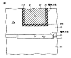
図3は、本発明の実施の形態に係る炭化珪素半導体装置1のオフ状態を説明するための図である。図3を参照して、炭化珪素半導体装置1(MOSFET)のオフ時には、ゲート電極30の電圧は、閾値電圧以下である。たとえばゲート電極30の電位は、ソース電極50の電位に等しい。すなわちゲート電極30の電圧は0Vである。
FIG. 3 is a diagram for describing an off state of silicon
炭化珪素半導体装置1のスイッチングによって、炭化珪素半導体装置1のオフ時には、高い電圧(たとえば1200V)がドレイン電極70に印加されうる。空乏層17a,13aがともにドリフト領域13側に拡がる。したがって、図3に例示されるように、空乏層13a,17aが合わさる。同じように、空乏層11a,17bが炭化珪素エピタキシャル層11側に拡がる。これにより、空乏層11a,17bが合わさる。
By switching silicon
炭化珪素エピタキシャル層11側に形成された空乏層によって、炭化珪素エピタキシャル層11における電界集中を緩和することができる。また、ドリフト領域13において、ゲート絶縁膜25の周囲の領域が空乏化されているので、ゲート絶縁膜25における電界集中を緩和することができる。これにより、アバランシェブレークダウンが生じたとしても、ゲート絶縁膜25が破壊する可能性を小さくすることができる。
Electric field concentration in silicon
図4は、本発明の実施の形態に係る炭化珪素半導体装置の比較例の一部を示した断面図である。図4を参照して、炭化珪素半導体装置101において、埋込領域17は、トレンチ21の底部21Bに接する。ターンオン時には、電流は、空乏層17aと空乏層13aとの間にある、空乏化されていない部分を流れる。しかしながら、空乏層17a,13aが、ドリフト領域13の側に拡がるため、チャネル14aの近傍では、電流の流れる経路が狭い。すなわちチャネル14aの近傍では、狭窄抵抗が生じる。チャネル14aの近傍の抵抗値が大きいために、オン抵抗が増大する。
FIG. 4 is a cross sectional view showing a part of a comparative example of the silicon carbide semiconductor device according to the embodiment of the present invention. Referring to FIG. 4, in silicon
これに対して、本発明の実施の形態によれば、埋込領域17と、トレンチ21の底部21Bとが離れている。したがって、炭化珪素半導体装置1のオン時のドレイン電圧によって、空乏層17a,13aがともにドリフト領域13の側に拡がる。しかし、図4に示された構成に比べて、本発明の実施の形態では、チャネル14aの近傍における電流の経路の幅が大きい。これにより、オン抵抗の増大を抑えることができる。
On the other hand, according to the embodiment of the present invention, the buried
オン抵抗の増大を抑える観点からは、トレンチ21の底部21Bから埋込領域17までの距離(図1に示したD1)は、少なくとも0.1μmであることが好ましい。オン抵抗の増大を抑える観点からは、距離D1が大きいほうが好ましい。一方では、距離D1が大きくなるほど、炭化珪素半導体装置1のオフ時において、ゲート絶縁膜25に、ゲート絶縁膜25の絶縁耐圧を上回る電圧が印加される可能性が高くなる。ゲート絶縁膜25に印加される電界を抑制する観点からは、距離D1は3.0μm以下であることが好ましい。このため、距離D1は、0.1μm≦D1≦3.0μmであることが好ましい。
From the viewpoint of suppressing an increase in on-resistance, the distance from the bottom 21B of the
ドリフト領域13(炭化珪素エピタキシャル層12)の不純物濃度ND2は、炭化珪素エピタキシャル層11の不純物濃度ND1よりも大きい(ND1<ND2)。これにより、炭化珪素半導体装置1のオン抵抗を下げることができる。埋込領域17の不純物濃度NBPが不純物濃度ND2よりも大きいので、ドレイン−ソース間に高電圧が印加された場合に、空乏層17aがドリフト領域13側に拡がる。この空乏層17aによって、ゲート絶縁膜25に印加される電界が著しく高くなることを抑制することができる。
Impurity concentration N D2 of drift region 13 (silicon carbide epitaxial layer 12) is higher than impurity concentration N D1 of silicon carbide epitaxial layer 11 (N D1 <N D2 ). Thereby, the on-resistance of silicon
埋込領域17の幅WBP2は、トレンチ21の底部21Bの幅Wtrenchよりも大きい(WBP2>Wtrench)。これにより、空乏層17aの幅も幅Wtrenchより大きくすることができるので、トレンチ21の底部21Bにおいて、ゲート絶縁膜25に印加される電界を低減することができる。さらに、トレンチ21の底部21Bにおけるゲート絶縁膜25の厚さtg1は、トレンチ21の側壁面21Aにおけるゲート絶縁膜25の厚さtg2よりも大きい(tg2<tg1)。これにより、アバランシェブレークダウンが生じたときに、ゲート絶縁膜25に印加される電界を下げることができる。したがって、アバランシェブレークダウンが生じたときに、ゲート絶縁膜25が破壊される可能性をより小さくすることができる。
The width W BP2 of the buried
さらに埋込領域18の幅WBP1は、埋込領域17の幅WBP2よりも小さい(WBP1<WBP2)。このように幅WBP1および幅WBP2の間の関係を定義することにより、埋込領域17の直下の領域に比べて、埋込領域18の直下の領域のほうが、アバランシェブレークダウンが発生しやすい。埋込領域18の直下の領域においてアバランシェブレークダウンが発生した場合、ブレークダウン電流は、埋込領域18およびディープ領域16を経由してソース電極50へと流れる。ブレークダウン電流が、トレンチ21の底を流れないので、ゲート絶縁膜25の破壊を防ぐ効果がより高められる。
Further, the width W BP1 of the buried
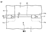
図3に示されるように、所定の高電圧(たとえば1200V)がドレイン電極70に印加された場合に、埋込領域17が完全に空乏化しないように、埋込領域17の不純物濃度NBPが定められる。さらに、ゲート電極30の電位が0Vである。
As shown in FIG. 3, when a predetermined high voltage (for example, 1200 V) is applied to the
図5は、本発明の実施の形態に係る炭化珪素半導体装置に逆バイアス電圧が印加された時にトレンチ21の底部21Bの近傍に印加される電圧を説明するための部分拡大図である。図5に示されるように、炭化珪素半導体装置1がオフしたときには、ゲート電極30の電圧は0Vである。トレンチ21の底部21Bと埋込領域17との間の領域が空乏化されて、空乏層17aが形成される。空乏層17a内には電位分布が生じる。一方、埋込領域17には、空乏化されていない部分が存在する。この部分の電圧は0Vである。ゲート電極30および埋込領域17の空乏化されていない部分の電圧が0Vであるので、ゲート電極30から深さ方向に沿った電界強度の傾きが小さくなる。したがって、トレンチ21の底部21Bに配置されたゲート絶縁膜25の部分に印加される電界を小さくすることができる。なお、埋込領域17が完全に空乏化した場合には、埋込領域17の内部にも電位分布が生じるため、ゲート電極30から深さ方向に沿った電界強度の傾きが大きくなる。このためトレンチ21の底部21Bに配置されたゲート絶縁膜25の部分に印加される電界が大きくなる。
FIG. 5 is a partial enlarged view for illustrating a voltage applied in the vicinity of
本発明の実施の形態によれば、埋込領域17の不純物濃度NBPは、ドリフト領域13の不純物濃度ND2よりも大きい(ND2<NBP)。これにより所定の高電圧(たとえば1200V)がドレイン電極70に印加された場合にも、埋込領域17が完全に空乏化しにくくなる。したがって、高い電界によってゲート絶縁膜25が破壊する可能性を小さくすることができる。
According to the embodiment of the present invention, the impurity concentration N BP of the buried
さらに、本発明の実施の形態によれば、埋込領域20の不純物濃度NJは、不純物濃度ND2よりも大きい(ND2<NJ)。これにより、炭化珪素半導体装置1のオン抵抗を下げることができる。一方で、不純物濃度NJは、埋込領域17の不純物濃度NBPよりも小さい(NJ<NBP)。これにより、空乏層は、埋込領域17と埋込領域20との接合面から埋込領域20側に拡がるので、埋込領域17が完全に空乏化しにくくなる。
Furthermore, according to the embodiment of the present invention, the impurity concentration N J of the buried
図6は、本発明の実施の形態に係る炭化珪素半導体装置の比較例の構成を説明するための部分拡大図である。図6に示されるように、空乏層11a,17aは炭化珪素エピタキシャル層11側に拡がる。矢印は、炭化珪素エピタキシャル層11を流れる電流を表す。DJ>DBPである場合には、電流の流れる経路が狭くなるので、抵抗値が高くなる。この結果、炭化珪素半導体装置のオン抵抗は高い。
FIG. 6 is a partially enlarged view for illustrating a configuration of a comparative example of the silicon carbide semiconductor device according to the embodiment of the present invention. As shown in FIG. 6,
一方、本発明の実施の形態では、界面11Aからの埋込領域20の深さDJは、埋込領域17,18の各々の界面11Aからの深さDBPよりも小さい(DJ<DBP)。図7は、本発明の実施の形態に係る炭化珪素半導体装置のオン時に流れる電流を説明するための部分拡大図である。図7に示されるように、DJ<DBPである場合には、空乏層11a,17aが炭化珪素エピタキシャル層11側に拡がったとしても、電流の流れる経路の幅が大きい。したがって、炭化珪素半導体装置1のオン抵抗が上昇することを抑えることができる。
On the other hand, in the embodiment of the present invention, the depth D J of the buried
なお、本発明の実施の形態では、トレンチ21の形状は、図1等に示された形状に限定されるものではない。図8は、本発明の実施の形態に係る炭化珪素半導体装置の別の構成の例を示した断面図である。図8に示されるように、対向する2つの側壁面21Aは、主面12Aに対して傾斜する。
In the embodiment of the present invention, the shape of the
側壁面21Aは、たとえば{000−1}面に対して50度以上80度以下傾斜した面である。より具体的には、側壁面21Aは、巨視的に見て、面方位{0−33−8}、{0−11−2}、{0−11−4}および{0−11−1}のいずれかを有し得る。なお、「巨視的」とは、原子間隔程度の寸法を有する微細構造を無視することを意味する。このように巨視的なオフ角の測定としては、たとえば、一般的なX線回折を用いた方法を用い得る。上記の面を採用することによって、炭化珪素半導体装置1のオン抵抗をさらに低減することができる。
The
さらに、本発明の実施の形態に係る炭化珪素半導体装置1は、MOSFETであると限定されるものではない。図9は、本発明の実施の形態に係る炭化珪素半導体装置のさらに別の構成の例を示した断面図である。図9に示されるように、本発明の実施の形態に係る炭化珪素半導体装置1は、IGBTであってもよい。図9に示された構成によれば、炭化珪素基板10の導電型はp型である。この点において、図9に示されたIGBTは、図1に示されたMOSFETと相違する。
Furthermore, silicon
炭化珪素半導体装置1がIGBTである場合にも、トレンチ21の形状は特に限定されるものではない。図10は、図9に示されたIGBTの変形例を示した図である。図8および図10の比較から理解されるように、IGBTのトレンチ21は、主面12Aに向かってテーパ状に拡がるように形成され、対向する2つの側壁面21Aを有していてもよい。2つの側壁面21Aは、たとえば{000−1}面に対して50度以上80度以下傾斜した面であり、上記の面方位{0−33−8}、{0−11−2}、{0−11−4}および{0−11−1}のいずれかを有し得る。
Even when silicon
さらに、上記の説明では、第1の導電型はn型であり、第2の導電型はp型であるが、第1の導電型がp型であり、第2の導電型がn型であってもよい。 Further, in the above description, the first conductivity type is n-type and the second conductivity type is p-type, but the first conductivity type is p-type and the second conductivity type is n-type. There may be.
今回開示された実施の形態はすべての点で例示であって、制限的なものではないと考えられるべきである。本発明の範囲は上記した実施の形態ではなく特許請求の範囲によって示され、特許請求の範囲と均等の意味、および範囲内でのすべての変更が含まれることが意図される。 The embodiment disclosed this time is to be considered as illustrative in all points and not restrictive. The scope of the present invention is shown not by the above-described embodiment but by the scope of claims, and is intended to include meanings equivalent to the scope of claims and all modifications within the scope.
1,101 炭化珪素半導体装置
10 炭化珪素基板
10A,10B,12A 主面
11,12 炭化珪素エピタキシャル層
11A 界面
11a,13a,17a,17b 空乏層
13 ドリフト領域
14 ボディ領域
14a チャネル
15 ソース領域
16 ディープ領域
16B 底部(ディープ領域)
17,18,20 埋込領域
21 トレンチ
21A 側壁面
21B 底部(トレンチ)
25 ゲート絶縁膜
30 ゲート電極
40 層間絶縁膜
50 ソース電極
70 ドレイン電極
D1 距離
DBP,DJ 深さ
NBP,ND1,ND2,NJ 不純物濃度
WBP1,WBP2,WJ,Wtrench 幅
t1,t2,tg1,tg2 厚さ
DESCRIPTION OF SYMBOLS 1,101 Silicon
17, 18, 20 Embedded
25
Claims (11)
炭化珪素基板と、
前記炭化珪素基板上に配置され、第1の導電型を有する、第1の炭化珪素層と、
前記第1の炭化珪素層上に配置され、前記第1の導電型を有する第2の炭化珪素層と、
前記第2の炭化珪素層上に配置され、前記第1の導電型と異なる第2の導電型を有する、第3の炭化珪素層と、
前記第3の炭化珪素層上に配置され、前記第1の導電型を有する、第4の炭化珪素層と、
前記第2の炭化珪素層、前記第3の炭化珪素層および前記第4の炭化珪素層を貫通するように形成され、前記第2の導電型を有する第1の不純物領域とを備え、
トレンチが、前記第4の炭化珪素層から前記第3の炭化珪素層を貫通して前記第2の炭化珪素層に達するように、前記炭化珪素半導体装置に形成され、
前記炭化珪素半導体装置は、
前記トレンチの壁に接触したゲート絶縁膜と、
前記ゲート絶縁膜に接触し、かつ、前記トレンチに充填されたゲート電極と、
前記トレンチの下方に前記トレンチの底部から離間して配置され、前記第2の導電型を有する、第2の不純物領域と、
前記第1の不純物領域に接するように前記第1の不純物領域の下方に形成され、前記第2の導電型を有し、かつ、前記第2の不純物領域に電気的に接続された第3の不純物領域と、
前記第2の不純物領域と前記第3の不純物領域との間に形成され、前記第1の導電型を有する第4の不純物領域とを備える、炭化珪素半導体装置。 A silicon carbide semiconductor device,
A silicon carbide substrate;
A first silicon carbide layer disposed on the silicon carbide substrate and having a first conductivity type;
A second silicon carbide layer disposed on the first silicon carbide layer and having the first conductivity type;
A third silicon carbide layer disposed on the second silicon carbide layer and having a second conductivity type different from the first conductivity type;
A fourth silicon carbide layer disposed on the third silicon carbide layer and having the first conductivity type;
A first impurity region formed so as to penetrate the second silicon carbide layer, the third silicon carbide layer, and the fourth silicon carbide layer, and having the second conductivity type,
A trench is formed in the silicon carbide semiconductor device so as to reach the second silicon carbide layer from the fourth silicon carbide layer through the third silicon carbide layer;
The silicon carbide semiconductor device is
A gate insulating film in contact with the trench wall;
A gate electrode in contact with the gate insulating film and filled in the trench;
A second impurity region disposed below the trench and spaced from the bottom of the trench and having the second conductivity type;
The third impurity region is formed below the first impurity region so as to be in contact with the first impurity region, has the second conductivity type, and is electrically connected to the second impurity region. An impurity region;
A silicon carbide semiconductor device comprising: a fourth impurity region formed between the second impurity region and the third impurity region and having the first conductivity type.
前記第4の不純物領域の不純物濃度は、前記第2の炭化珪素層の不純物濃度よりも大きく、
前記第2の不純物領域の不純物濃度は、前記第4の不純物領域の不純物濃度よりも大きい、請求項1に記載の炭化珪素半導体装置。 The impurity concentration of the second silicon carbide layer is greater than the impurity concentration of the first silicon carbide layer,
The impurity concentration of the fourth impurity region is greater than the impurity concentration of the second silicon carbide layer,
2. The silicon carbide semiconductor device according to claim 1, wherein an impurity concentration of the second impurity region is higher than an impurity concentration of the fourth impurity region.
0.1μm≦D1≦3.0μm
の関係が成り立つ、請求項1から請求項3のいずれか1項に記載の炭化珪素半導体装置。 Denoting the distance from the bottom of the trench to the second impurity region as D 1 ,
0.1 μm ≦ D 1 ≦ 3.0 μm
The silicon carbide semiconductor device according to any one of claims 1 to 3, wherein the relationship is established.
前記炭化珪素基板は、前記第1の導電型を有する、請求項1から請求項9のいずれか1項に記載の炭化珪素半導体装置。 The silicon carbide semiconductor device is a MOSFET,
The silicon carbide semiconductor device according to any one of claims 1 to 9, wherein the silicon carbide substrate has the first conductivity type.
前記炭化珪素基板は、前記第2の導電型を有する、請求項1から請求項9のいずれか1項に記載の炭化珪素半導体装置。 The silicon carbide semiconductor device is an IGBT,
10. The silicon carbide semiconductor device according to claim 1, wherein said silicon carbide substrate has said second conductivity type.
Priority Applications (3)
| Application Number | Priority Date | Filing Date | Title |
|---|---|---|---|
| JP2016071217A JP6708954B2 (en) | 2016-03-31 | 2016-03-31 | Silicon carbide semiconductor device |
| US16/089,448 US10756168B2 (en) | 2016-03-31 | 2017-02-02 | Silicon carbide semiconductor device |
| PCT/JP2017/003712 WO2017169085A1 (en) | 2016-03-31 | 2017-02-02 | Silicon carbide semiconductor device |
Applications Claiming Priority (1)
| Application Number | Priority Date | Filing Date | Title |
|---|---|---|---|
| JP2016071217A JP6708954B2 (en) | 2016-03-31 | 2016-03-31 | Silicon carbide semiconductor device |
Publications (2)
| Publication Number | Publication Date |
|---|---|
| JP2017183604A true JP2017183604A (en) | 2017-10-05 |
| JP6708954B2 JP6708954B2 (en) | 2020-06-10 |
Family
ID=59963844
Family Applications (1)
| Application Number | Title | Priority Date | Filing Date |
|---|---|---|---|
| JP2016071217A Active JP6708954B2 (en) | 2016-03-31 | 2016-03-31 | Silicon carbide semiconductor device |
Country Status (3)
| Country | Link |
|---|---|
| US (1) | US10756168B2 (en) |
| JP (1) | JP6708954B2 (en) |
| WO (1) | WO2017169085A1 (en) |
Cited By (4)
| Publication number | Priority date | Publication date | Assignee | Title |
|---|---|---|---|---|
| CN110098258A (en) * | 2018-01-29 | 2019-08-06 | 瑞萨电子株式会社 | Semiconductor devices and its manufacturing method |
| JP2019140259A (en) * | 2018-02-09 | 2019-08-22 | 富士電機株式会社 | Semiconductor device and method for manufacturing semiconductor device |
| JP2021141265A (en) * | 2020-03-09 | 2021-09-16 | 三菱電機株式会社 | Semiconductor device |
| JP2022534924A (en) * | 2019-05-27 | 2022-08-04 | ロベルト・ボッシュ・ゲゼルシャフト・ミト・ベシュレンクテル・ハフツング | Power transistor manufacturing method and power transistor |
Families Citing this family (6)
| Publication number | Priority date | Publication date | Assignee | Title |
|---|---|---|---|---|
| JP6658406B2 (en) * | 2016-08-31 | 2020-03-04 | 株式会社デンソー | Method for manufacturing silicon carbide semiconductor device |
| US10777676B2 (en) * | 2016-11-11 | 2020-09-15 | Sumitomo Electric Industries, Ltd. | Silicon carbide semiconductor device |
| JP7073873B2 (en) * | 2018-04-13 | 2022-05-24 | 株式会社デンソー | Switching element |
| GB2589543A (en) * | 2019-09-09 | 2021-06-09 | Mqsemi Ag | Method for forming a low injection P-type contact region and power semiconductor devices with the same |
| JP7169459B2 (en) * | 2019-10-11 | 2022-11-10 | 株式会社デンソー | switching element |
| CN113990919A (en) * | 2021-10-12 | 2022-01-28 | 松山湖材料实验室 | Silicon carbide semiconductor structure, device and preparation method |
Citations (11)
| Publication number | Priority date | Publication date | Assignee | Title |
|---|---|---|---|---|
| JP2009117593A (en) * | 2007-11-06 | 2009-05-28 | Denso Corp | Silicon carbide semiconductor apparatus and method of manufacturing the same |
| JP2011100967A (en) * | 2009-07-21 | 2011-05-19 | Rohm Co Ltd | Semiconductor device |
| JP2012038770A (en) * | 2010-08-03 | 2012-02-23 | Sumitomo Electric Ind Ltd | Semiconductor device and method of manufacturing the same |
| JP2013145770A (en) * | 2012-01-13 | 2013-07-25 | Sumitomo Electric Ind Ltd | Semiconductor device and manufacturing method of the same |
| JP2013219161A (en) * | 2012-04-09 | 2013-10-24 | Mitsubishi Electric Corp | Semiconductor device and semiconductor device manufacturing method |
| JP2014053595A (en) * | 2012-08-07 | 2014-03-20 | Denso Corp | Silicon carbide semiconductor device and manufacturing method of the same |
| JP2015026726A (en) * | 2013-07-26 | 2015-02-05 | 住友電気工業株式会社 | Silicon carbide semiconductor device and method of manufacturing the same |
| JP2015220408A (en) * | 2014-05-20 | 2015-12-07 | 住友電気工業株式会社 | Silicon carbide semiconductor device and manufacturing method of the same |
| WO2016002769A1 (en) * | 2014-06-30 | 2016-01-07 | 国立研究開発法人産業技術総合研究所 | Silicon carbide semiconductor device and production method for same |
| WO2016002766A1 (en) * | 2014-06-30 | 2016-01-07 | 国立研究開発法人産業技術総合研究所 | Silicon carbide semiconductor device and production method for same |
| WO2016038833A1 (en) * | 2014-09-08 | 2016-03-17 | パナソニックIpマネジメント株式会社 | Semiconductor device and method for manufacturing same |
Family Cites Families (4)
| Publication number | Priority date | Publication date | Assignee | Title |
|---|---|---|---|---|
| JP2012099601A (en) | 2010-11-01 | 2012-05-24 | Sumitomo Electric Ind Ltd | Semiconductor device and method of manufacturing the same |
| US9224860B2 (en) | 2010-12-10 | 2015-12-29 | Mitsubishi Electric Corporation | Trench-gate type semiconductor device and manufacturing method therefor |
| JP2013069964A (en) | 2011-09-26 | 2013-04-18 | Sumitomo Electric Ind Ltd | Silicon carbide semiconductor device |
| JP6111673B2 (en) | 2012-07-25 | 2017-04-12 | 住友電気工業株式会社 | Silicon carbide semiconductor device |
-
2016
- 2016-03-31 JP JP2016071217A patent/JP6708954B2/en active Active
-
2017
- 2017-02-02 WO PCT/JP2017/003712 patent/WO2017169085A1/en active Application Filing
- 2017-02-02 US US16/089,448 patent/US10756168B2/en active Active
Patent Citations (11)
| Publication number | Priority date | Publication date | Assignee | Title |
|---|---|---|---|---|
| JP2009117593A (en) * | 2007-11-06 | 2009-05-28 | Denso Corp | Silicon carbide semiconductor apparatus and method of manufacturing the same |
| JP2011100967A (en) * | 2009-07-21 | 2011-05-19 | Rohm Co Ltd | Semiconductor device |
| JP2012038770A (en) * | 2010-08-03 | 2012-02-23 | Sumitomo Electric Ind Ltd | Semiconductor device and method of manufacturing the same |
| JP2013145770A (en) * | 2012-01-13 | 2013-07-25 | Sumitomo Electric Ind Ltd | Semiconductor device and manufacturing method of the same |
| JP2013219161A (en) * | 2012-04-09 | 2013-10-24 | Mitsubishi Electric Corp | Semiconductor device and semiconductor device manufacturing method |
| JP2014053595A (en) * | 2012-08-07 | 2014-03-20 | Denso Corp | Silicon carbide semiconductor device and manufacturing method of the same |
| JP2015026726A (en) * | 2013-07-26 | 2015-02-05 | 住友電気工業株式会社 | Silicon carbide semiconductor device and method of manufacturing the same |
| JP2015220408A (en) * | 2014-05-20 | 2015-12-07 | 住友電気工業株式会社 | Silicon carbide semiconductor device and manufacturing method of the same |
| WO2016002769A1 (en) * | 2014-06-30 | 2016-01-07 | 国立研究開発法人産業技術総合研究所 | Silicon carbide semiconductor device and production method for same |
| WO2016002766A1 (en) * | 2014-06-30 | 2016-01-07 | 国立研究開発法人産業技術総合研究所 | Silicon carbide semiconductor device and production method for same |
| WO2016038833A1 (en) * | 2014-09-08 | 2016-03-17 | パナソニックIpマネジメント株式会社 | Semiconductor device and method for manufacturing same |
Cited By (6)
| Publication number | Priority date | Publication date | Assignee | Title |
|---|---|---|---|---|
| CN110098258A (en) * | 2018-01-29 | 2019-08-06 | 瑞萨电子株式会社 | Semiconductor devices and its manufacturing method |
| JP2019140259A (en) * | 2018-02-09 | 2019-08-22 | 富士電機株式会社 | Semiconductor device and method for manufacturing semiconductor device |
| JP7106882B2 (en) | 2018-02-09 | 2022-07-27 | 富士電機株式会社 | Semiconductor device and method for manufacturing semiconductor device |
| JP2022534924A (en) * | 2019-05-27 | 2022-08-04 | ロベルト・ボッシュ・ゲゼルシャフト・ミト・ベシュレンクテル・ハフツング | Power transistor manufacturing method and power transistor |
| JP2021141265A (en) * | 2020-03-09 | 2021-09-16 | 三菱電機株式会社 | Semiconductor device |
| JP7442932B2 (en) | 2020-03-09 | 2024-03-05 | 三菱電機株式会社 | semiconductor equipment |
Also Published As
| Publication number | Publication date |
|---|---|
| US10756168B2 (en) | 2020-08-25 |
| US20190237536A1 (en) | 2019-08-01 |
| WO2017169085A1 (en) | 2017-10-05 |
| JP6708954B2 (en) | 2020-06-10 |
Similar Documents
| Publication | Publication Date | Title |
|---|---|---|
| WO2017169085A1 (en) | Silicon carbide semiconductor device | |
| JP6400778B2 (en) | Insulated gate type silicon carbide semiconductor device and method of manufacturing the same | |
| JP6197995B2 (en) | Wide band gap insulated gate semiconductor device | |
| JP5668576B2 (en) | Silicon carbide semiconductor device | |
| JP5840308B2 (en) | Silicon carbide semiconductor device and manufacturing method thereof | |
| JP2001135819A (en) | Super-junction semiconductor element | |
| JP6323556B2 (en) | Semiconductor device | |
| JP2005183563A (en) | Semiconductor device | |
| JP5297706B2 (en) | Semiconductor device | |
| JP7139678B2 (en) | Silicon carbide semiconductor device | |
| WO2015141212A1 (en) | Semiconductor device | |
| JP5729400B2 (en) | Manufacturing method of semiconductor device | |
| US10199457B2 (en) | Silicon carbide semiconductor device | |
| US9178021B1 (en) | Silicon carbide semiconductor device | |
| JP4595327B2 (en) | Semiconductor element | |
| JP7051890B2 (en) | Wide gap semiconductor device | |
| JP2010093080A (en) | Semiconductor device | |
| US20150171169A1 (en) | Semiconductor device | |
| JP6651801B2 (en) | Semiconductor device and method of manufacturing semiconductor device | |
| JP2009111237A (en) | Semiconductor device | |
| JP2014192242A (en) | Semiconductor device | |
| JP5082260B2 (en) | Silicon carbide semiconductor device |
Legal Events
| Date | Code | Title | Description |
|---|---|---|---|
| A621 | Written request for application examination |
Free format text: JAPANESE INTERMEDIATE CODE: A621 Effective date: 20181022 |
|
| A131 | Notification of reasons for refusal |
Free format text: JAPANESE INTERMEDIATE CODE: A131 Effective date: 20191217 |
|
| A521 | Request for written amendment filed |
Free format text: JAPANESE INTERMEDIATE CODE: A523 Effective date: 20200120 |
|
| TRDD | Decision of grant or rejection written | ||
| A01 | Written decision to grant a patent or to grant a registration (utility model) |
Free format text: JAPANESE INTERMEDIATE CODE: A01 Effective date: 20200422 |
|
| A61 | First payment of annual fees (during grant procedure) |
Free format text: JAPANESE INTERMEDIATE CODE: A61 Effective date: 20200505 |
|
| R150 | Certificate of patent or registration of utility model |
Ref document number: 6708954 Country of ref document: JP Free format text: JAPANESE INTERMEDIATE CODE: R150 |
|
| R250 | Receipt of annual fees |
Free format text: JAPANESE INTERMEDIATE CODE: R250 |