JP2017181554A - 光モジュール、及び光モジュールの調心方法 - Google Patents
光モジュール、及び光モジュールの調心方法 Download PDFInfo
- Publication number
- JP2017181554A JP2017181554A JP2016063802A JP2016063802A JP2017181554A JP 2017181554 A JP2017181554 A JP 2017181554A JP 2016063802 A JP2016063802 A JP 2016063802A JP 2016063802 A JP2016063802 A JP 2016063802A JP 2017181554 A JP2017181554 A JP 2017181554A
- Authority
- JP
- Japan
- Prior art keywords
- optical
- optical element
- ferrule
- module
- conversion
- Prior art date
- Legal status (The legal status is an assumption and is not a legal conclusion. Google has not performed a legal analysis and makes no representation as to the accuracy of the status listed.)
- Granted
Links
Images


Classifications
-
- G—PHYSICS
- G02—OPTICS
- G02B—OPTICAL ELEMENTS, SYSTEMS OR APPARATUS
- G02B6/00—Light guides; Structural details of arrangements comprising light guides and other optical elements, e.g. couplings
- G02B6/24—Coupling light guides
- G02B6/42—Coupling light guides with opto-electronic elements
- G02B6/4201—Packages, e.g. shape, construction, internal or external details
- G02B6/4256—Details of housings
-
- G—PHYSICS
- G02—OPTICS
- G02B—OPTICAL ELEMENTS, SYSTEMS OR APPARATUS
- G02B6/00—Light guides; Structural details of arrangements comprising light guides and other optical elements, e.g. couplings
- G02B6/24—Coupling light guides
- G02B6/42—Coupling light guides with opto-electronic elements
- G02B6/4201—Packages, e.g. shape, construction, internal or external details
- G02B6/4219—Mechanical fixtures for holding or positioning the elements relative to each other in the couplings; Alignment methods for the elements, e.g. measuring or observing methods especially used therefor
-
- G—PHYSICS
- G02—OPTICS
- G02B—OPTICAL ELEMENTS, SYSTEMS OR APPARATUS
- G02B6/00—Light guides; Structural details of arrangements comprising light guides and other optical elements, e.g. couplings
- G02B6/24—Coupling light guides
- G02B6/26—Optical coupling means
- G02B6/32—Optical coupling means having lens focusing means positioned between opposed fibre ends
-
- G—PHYSICS
- G02—OPTICS
- G02B—OPTICAL ELEMENTS, SYSTEMS OR APPARATUS
- G02B6/00—Light guides; Structural details of arrangements comprising light guides and other optical elements, e.g. couplings
- G02B6/24—Coupling light guides
- G02B6/42—Coupling light guides with opto-electronic elements
- G02B6/4201—Packages, e.g. shape, construction, internal or external details
- G02B6/4204—Packages, e.g. shape, construction, internal or external details the coupling comprising intermediate optical elements, e.g. lenses, holograms
- G02B6/421—Packages, e.g. shape, construction, internal or external details the coupling comprising intermediate optical elements, e.g. lenses, holograms the intermediate optical component consisting of a short length of fibre, e.g. fibre stub
-
- G—PHYSICS
- G02—OPTICS
- G02B—OPTICAL ELEMENTS, SYSTEMS OR APPARATUS
- G02B6/00—Light guides; Structural details of arrangements comprising light guides and other optical elements, e.g. couplings
- G02B6/24—Coupling light guides
- G02B6/42—Coupling light guides with opto-electronic elements
- G02B6/4201—Packages, e.g. shape, construction, internal or external details
- G02B6/4204—Packages, e.g. shape, construction, internal or external details the coupling comprising intermediate optical elements, e.g. lenses, holograms
- G02B6/4215—Packages, e.g. shape, construction, internal or external details the coupling comprising intermediate optical elements, e.g. lenses, holograms the intermediate optical elements being wavelength selective optical elements, e.g. variable wavelength optical modules or wavelength lockers
-
- G—PHYSICS
- G02—OPTICS
- G02B—OPTICAL ELEMENTS, SYSTEMS OR APPARATUS
- G02B6/00—Light guides; Structural details of arrangements comprising light guides and other optical elements, e.g. couplings
- G02B6/24—Coupling light guides
- G02B6/42—Coupling light guides with opto-electronic elements
- G02B6/4201—Packages, e.g. shape, construction, internal or external details
- G02B6/4219—Mechanical fixtures for holding or positioning the elements relative to each other in the couplings; Alignment methods for the elements, e.g. measuring or observing methods especially used therefor
- G02B6/4236—Fixing or mounting methods of the aligned elements
- G02B6/424—Mounting of the optical light guide
-
- G—PHYSICS
- G02—OPTICS
- G02B—OPTICAL ELEMENTS, SYSTEMS OR APPARATUS
- G02B6/00—Light guides; Structural details of arrangements comprising light guides and other optical elements, e.g. couplings
- G02B6/24—Coupling light guides
- G02B6/42—Coupling light guides with opto-electronic elements
- G02B6/4292—Coupling light guides with opto-electronic elements the light guide being disconnectable from the opto-electronic element, e.g. mutually self aligning arrangements
-
- G—PHYSICS
- G02—OPTICS
- G02B—OPTICAL ELEMENTS, SYSTEMS OR APPARATUS
- G02B6/00—Light guides; Structural details of arrangements comprising light guides and other optical elements, e.g. couplings
- G02B6/24—Coupling light guides
- G02B6/42—Coupling light guides with opto-electronic elements
- G02B6/4201—Packages, e.g. shape, construction, internal or external details
- G02B6/4219—Mechanical fixtures for holding or positioning the elements relative to each other in the couplings; Alignment methods for the elements, e.g. measuring or observing methods especially used therefor
- G02B6/4236—Fixing or mounting methods of the aligned elements
- G02B6/4245—Mounting of the opto-electronic elements
-
- G—PHYSICS
- G02—OPTICS
- G02B—OPTICAL ELEMENTS, SYSTEMS OR APPARATUS
- G02B6/00—Light guides; Structural details of arrangements comprising light guides and other optical elements, e.g. couplings
- G02B6/24—Coupling light guides
- G02B6/42—Coupling light guides with opto-electronic elements
- G02B6/4201—Packages, e.g. shape, construction, internal or external details
- G02B6/4256—Details of housings
- G02B6/4262—Details of housings characterised by the shape of the housing
- G02B6/4263—Details of housings characterised by the shape of the housing of the transisitor outline [TO] can type
Abstract
【解決手段】複数の第1光素子部と、複数の第1光素子部それぞれと光学的に接合する、第2光素子部と、を備える、光モジュールであって、複数の第1光素子部それぞれは、光信号又は電気信号のうち一方から他方へ変換する変換光素子と、先端が第2光素子部と接して光学的に接合するフェルールと、フェルールと変換光素子とを、光学的に調整する位置に配置される、第1光学系と、を備え、第2光素子部は、複数の第1光素子部それぞれのフェルールの先端と接合箇所にて接触して接合する、複数の接合部と、複数の第1光素子部それぞれの変換光素子と、光学的に接合する、波長多重光素子と、波長多重光素子と、前記複数の接合部それぞれの前記接合箇所とを、光学的に調整する位置にそれぞれ配置される、複数の第2光学系と、を備える。
【選択図】図3
Description
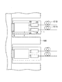
図1は、本発明の第1の実施形態に係る光モジュール1の構成を示す模式図である。当該実施形態に係る光モジュール1は、送信機能及び受信機能を有するトランシーバであり、光送信モジュール2Aと、光受信モジュール2Bと、フレキシブル基板3A,3Bと、プリント回路基板4と、電気コネクタ5と、を備えている。
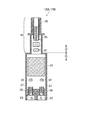
図6は、本発明の第2の実施形態にかかる光MUXモジュール15A/光DeMUXモジュール15Bの構造を示す模式断面図である。当該実施形態に係る光モジュール1は、第2光素子部の複数の接合部の構造が異なっている以外は、第1の実施形態と同じである。図6に示す通り、複数の接合部(例えば、設置部22,23)は、第1光素子部のフェルールと光学的に結合するためのスリーブ機構を有している。ここで、スリーブ機構は、光ファイバスタブ37と、スリーブ38と、を備え、光ファイバスタブ37の一端(図6に示す下端:Qで示す部分)が、第1光素子部のフェルールの先端(図3にPで示す部分)と接触するよう、光学的に接合される。スリーブ38は、例えば、割スリーブである。複数の第1光素子部が第2光素子部に収納されると、第1光素子部のフェルールの先端にあるコアの中心位置が光ファイバスタブ37の一端にあるコアの中心位置とを高精度で近づけるよう制御できる。理想的には、両方のコアの中心位置を一致させることができる。これにより、第1光素子部のフェルールと第2光素子部の接合部とを、さらに高精度で光学的に接合することができる。
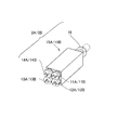
21,22,23,24 設置部、25 フェルール、26A LD素子、26B PD素子、27 集光レンズ、31 光合分波器、32 レンズ、33 集光レンズ、34 光アイソレータ、35,37 光ファイバスタブ、36,38 スリーブ、100 伝送装置、101,101A,101B 光ファイバ。
Claims (8)
- 複数の第1光素子部と、
前記複数の第1光素子部それぞれと光学的に接合する、第2光素子部と、
を備える、光モジュールであって、
前記複数の第1光素子部それぞれは、
光信号又は電気信号のうち一方から他方へ変換する変換光素子と、
先端が前記第2光素子部と接して光学的に接合するフェルールと、
前記フェルールと前記変換光素子とを、光学的に調整する位置に配置される、第1光学系と、
を備え、
前記第2光素子部は、
前記複数の第1光素子部それぞれの前記フェルールの先端と接合箇所にて接触して接合する、複数の接合部と、
前記複数の第1光素子部それぞれの前記変換光素子と、光学的に接合する、波長多重光素子と、
前記波長多重光素子と、前記複数の接合部それぞれの前記接合箇所とを、光学的に調整する位置にそれぞれ配置される、複数の第2光学系と、
を備える、
ことを特徴とする、光モジュール。 - 請求項1に記載の光モジュールであって、
前記複数の第1光素子部それぞれの前記変換光素子は、電気信号から光信号に変換する発光素子である、
ことを特徴とする、光モジュール。 - 請求項1に記載の光モジュールであって、
前記複数の第1光素子部それぞれの前記変換光素子は、光信号から電気信号に変換する受光素子である、
ことを特徴とする、光モジュール。 - 請求項1乃至3のいずれかに記載の光モジュールであって、
前記第2光素子部の前記複数の第2光学系それぞれは、凸レンズである。
ことを特徴とする、光モジュール。 - 請求項1乃至4のいずれかに記載の光モジュールであって、
前記複数の第1光素子部は、4つの第1光素子部であり、
前記第2光素子部の前記複数の接合部は、4つの接合部である、
ことを特徴とする、光モジュール。 - 請求項5に記載の光モジュールであって、
前記4つの接合部は、縦2つ及び横2つに並ぶ、
ことを特徴とする、光モジュール。 - 請求項1乃至6に記載の光モジュールであって、
前記複数の接合部それぞれは、スリーブ機構を有する、
ことを特徴とする、光モジュール。 - 複数の第1光素子部と、
前記複数の第1光素子部それぞれと光学的に接合する、第2光素子部と、
を備える、光モジュールの調心方法であって、
前記複数の第1光素子部それぞれは、
光信号又は電気信号のうち一方から他方へ変換する変換光素子と、
先端が前記第2光素子部と接して光学的に接合するフェルールと、
前記フェルールと前記変換光素子とを、光学的に接合するための、第1光学系と、
を備え、
前記第2光素子部は、
前記複数の第1光素子部それぞれの前記フェルールの先端と接合箇所にて接触して接合する、複数の接合部と、
前記複数の第1光素子部それぞれの前記変換光素子と、光学的に接合する、波長多重光素子と、
前記波長多重光素子と、前記複数の接合部それぞれの前記接合箇所とを、光学的に接合するための、複数の第2光学系と、
を備え、
前記複数の第1光素子部のうち1つの第1光素子部を調心する第1光素子部調心ステップと、
前記第2光素子部を調心する第2光素子部調心ステップと、
を備え、
前記第1光素子部調心ステップは、
前記1つの第1光素子部の前記フェルールの先端と接触して接合する第1接続端子を有する、第1調心用光学器を、前記1つの第1光素子部に接続するステップと、
前記1つの第1光素子部の前記変換光素子と、前記第1光学系と、のいずれか又は両方の位置を調整するステップと、
を含み、
前記第2光素子部調心ステップは、
前記第2光素子部の前記複数の接合部のうち1つの接合部と接触して接合する第2接続端子を有する、第2調心用光学器を、前記1つの接合部に接続するステップと、
前記複数の第2光学系のうち前記1つの接合部に対応する1つの第2光学系と、前記波長多重光素子と、のいずれか又は両方の位置を調整するステップと、
を含む、
ことを特徴とする、光モジュールの調心方法。
Priority Applications (3)
| Application Number | Priority Date | Filing Date | Title |
|---|---|---|---|
| JP2016063802A JP6876373B2 (ja) | 2016-03-28 | 2016-03-28 | 光モジュール、及び光モジュールの調心方法 |
| US15/465,923 US10379303B2 (en) | 2016-03-28 | 2017-03-22 | Optical module and method for aligning optical module |
| CN201710188087.3A CN107238899B (zh) | 2016-03-28 | 2017-03-27 | 光模块及光模块的调心方法 |
Applications Claiming Priority (1)
| Application Number | Priority Date | Filing Date | Title |
|---|---|---|---|
| JP2016063802A JP6876373B2 (ja) | 2016-03-28 | 2016-03-28 | 光モジュール、及び光モジュールの調心方法 |
Publications (3)
| Publication Number | Publication Date |
|---|---|
| JP2017181554A true JP2017181554A (ja) | 2017-10-05 |
| JP2017181554A5 JP2017181554A5 (ja) | 2019-01-10 |
| JP6876373B2 JP6876373B2 (ja) | 2021-05-26 |
Family
ID=59897089
Family Applications (1)
| Application Number | Title | Priority Date | Filing Date |
|---|---|---|---|
| JP2016063802A Active JP6876373B2 (ja) | 2016-03-28 | 2016-03-28 | 光モジュール、及び光モジュールの調心方法 |
Country Status (3)
| Country | Link |
|---|---|
| US (1) | US10379303B2 (ja) |
| JP (1) | JP6876373B2 (ja) |
| CN (1) | CN107238899B (ja) |
Families Citing this family (6)
| Publication number | Priority date | Publication date | Assignee | Title |
|---|---|---|---|---|
| US10313045B2 (en) * | 2016-11-17 | 2019-06-04 | Alliance Fiber Optic Products, Inc. | Wavelength-division multiplexing optical assembly with increased lane density |
| US10551569B2 (en) | 2017-02-02 | 2020-02-04 | Alliance Fiber Optic Products, Inc. | Wavelength-division multiplexing optical assembly with multiple collimator sets |
| JP6982962B2 (ja) * | 2017-02-16 | 2021-12-17 | 日本ルメンタム株式会社 | 光モジュール |
| CN110556704A (zh) * | 2018-05-31 | 2019-12-10 | 深圳联品激光技术有限公司 | 一种光纤输出端子以及激光器 |
| CN113296198A (zh) * | 2020-02-21 | 2021-08-24 | 佑胜光电股份有限公司 | 光发射组件、光学收发模块及光纤缆线模块 |
| US11973580B2 (en) | 2021-09-30 | 2024-04-30 | Corning Research & Development Corporation | Redundant wavelength division multiplexing devices and methods for processing light using same |
Citations (7)
| Publication number | Priority date | Publication date | Assignee | Title |
|---|---|---|---|---|
| JPH11258453A (ja) * | 1998-03-12 | 1999-09-24 | Fujitsu Ltd | 偏光合成装置および偏光分離装置ならびに励起光出力装置 |
| JP2002333553A (ja) * | 2001-05-09 | 2002-11-22 | Sumitomo Electric Ind Ltd | 光モジュール、ファイバスタブ部品 |
| US20030215240A1 (en) * | 2002-04-03 | 2003-11-20 | Grann Eric B. | Optical WDM with single mode tolerance and low profile |
| JP2004179559A (ja) * | 2002-11-28 | 2004-06-24 | Kyocera Corp | 光モジュール及びそれを用いた光モジュールアセンブリ |
| JP2010061139A (ja) * | 2008-09-05 | 2010-03-18 | Sumitomo Electric Ind Ltd | 光モジュール |
| JP2013104983A (ja) * | 2011-11-11 | 2013-05-30 | Hitachi Cable Ltd | 光モジュール |
| JP2015032658A (ja) * | 2013-08-01 | 2015-02-16 | 三菱電機株式会社 | 波長多重伝送装置の製造方法、波長多重伝送装置 |
Family Cites Families (7)
| Publication number | Priority date | Publication date | Assignee | Title |
|---|---|---|---|---|
| JPH11231177A (ja) * | 1997-12-12 | 1999-08-27 | Oki Electric Ind Co Ltd | 光素子モジュール及び光素子モジュールの製造方法 |
| US7090412B2 (en) * | 2002-08-02 | 2006-08-15 | Sumitomo Electric Industries, Ltd. | Optical module |
| JP2006106680A (ja) * | 2004-09-10 | 2006-04-20 | Opnext Japan Inc | 光素子モジュール及び光送受信機 |
| CN102162915A (zh) | 2011-04-25 | 2011-08-24 | 南京信息职业技术学院 | 压控可变光衰减器 |
| JP5900133B2 (ja) | 2012-04-27 | 2016-04-06 | 日立金属株式会社 | 光モジュール |
| CN104678514B (zh) * | 2013-11-29 | 2017-01-04 | 台达电子工业股份有限公司 | 光收发模块 |
| CN103955030B (zh) | 2014-04-09 | 2015-10-28 | 天津大学 | 一种锥形折射的多通道光纤旋转连接器 |
-
2016
- 2016-03-28 JP JP2016063802A patent/JP6876373B2/ja active Active
-
2017
- 2017-03-22 US US15/465,923 patent/US10379303B2/en active Active
- 2017-03-27 CN CN201710188087.3A patent/CN107238899B/zh active Active
Patent Citations (7)
| Publication number | Priority date | Publication date | Assignee | Title |
|---|---|---|---|---|
| JPH11258453A (ja) * | 1998-03-12 | 1999-09-24 | Fujitsu Ltd | 偏光合成装置および偏光分離装置ならびに励起光出力装置 |
| JP2002333553A (ja) * | 2001-05-09 | 2002-11-22 | Sumitomo Electric Ind Ltd | 光モジュール、ファイバスタブ部品 |
| US20030215240A1 (en) * | 2002-04-03 | 2003-11-20 | Grann Eric B. | Optical WDM with single mode tolerance and low profile |
| JP2004179559A (ja) * | 2002-11-28 | 2004-06-24 | Kyocera Corp | 光モジュール及びそれを用いた光モジュールアセンブリ |
| JP2010061139A (ja) * | 2008-09-05 | 2010-03-18 | Sumitomo Electric Ind Ltd | 光モジュール |
| JP2013104983A (ja) * | 2011-11-11 | 2013-05-30 | Hitachi Cable Ltd | 光モジュール |
| JP2015032658A (ja) * | 2013-08-01 | 2015-02-16 | 三菱電機株式会社 | 波長多重伝送装置の製造方法、波長多重伝送装置 |
Also Published As
| Publication number | Publication date |
|---|---|
| CN107238899B (zh) | 2022-12-13 |
| JP6876373B2 (ja) | 2021-05-26 |
| US20170276889A1 (en) | 2017-09-28 |
| US10379303B2 (en) | 2019-08-13 |
| CN107238899A (zh) | 2017-10-10 |
Similar Documents
| Publication | Publication Date | Title |
|---|---|---|
| JP6876373B2 (ja) | 光モジュール、及び光モジュールの調心方法 | |
| US8380075B2 (en) | Optical transceiver module | |
| US10551569B2 (en) | Wavelength-division multiplexing optical assembly with multiple collimator sets | |
| US8540437B2 (en) | Multi-wavelength optical transmitting and receiving modules | |
| US7184621B1 (en) | Multi-wavelength transmitter optical sub assembly with integrated multiplexer | |
| US20190018206A1 (en) | High speed optical transceiver module | |
| US9804352B2 (en) | Coaxial transmitter optical subassembly (TOSA) with an optical fiber coupling receptacle | |
| US10313045B2 (en) | Wavelength-division multiplexing optical assembly with increased lane density | |
| CN107479144B (zh) | 具有直接对准光复用器输入端的光发射子组件(tosa)模块的光发射器或收发器 | |
| TWM484713U (zh) | 可替換式光發射模組及搭載有可替換式光發射模組的光收發器 | |
| US9709759B2 (en) | NxN parallel optical transceiver | |
| JP7091600B2 (ja) | 光受信モジュール | |
| US10884201B2 (en) | Receptacle configuration to support on-board receiver optical subassembly (ROSA) | |
| US20210349264A1 (en) | Integrated optical device based on coupling between optical chips | |
| JP4886819B2 (ja) | 3波長多重光送受信モジュール | |
| JP2009151041A (ja) | 光モジュールおよび光送受信モジュール | |
| US9274294B2 (en) | Optical communication module and method for producing the same | |
| US9225428B1 (en) | Method and system for alignment of photodetector array to optical demultiplexer outputs | |
| JP2019109380A (ja) | 光合分波器、光サブアセンブリ及び光モジュール | |
| US9804346B2 (en) | Receptacle-collimator assembly and multi-wavelength optical receiver module | |
| KR101908325B1 (ko) | 양방향 센싱 통신을 위한 광 송수신기 및 광 송수신기 제작방법 | |
| US10983291B2 (en) | Holder element with integrated optical arrangement to offset an output light path | |
| JP2004354908A (ja) | 双方向光通信モジュール | |
| JP2005257940A (ja) | Wdmフィルタモジュール | |
| JP2005315992A (ja) | 光トランシーバ構造 |
Legal Events
| Date | Code | Title | Description |
|---|---|---|---|
| A521 | Request for written amendment filed |
Free format text: JAPANESE INTERMEDIATE CODE: A523 Effective date: 20181126 |
|
| A621 | Written request for application examination |
Free format text: JAPANESE INTERMEDIATE CODE: A621 Effective date: 20181126 |
|
| A977 | Report on retrieval |
Free format text: JAPANESE INTERMEDIATE CODE: A971007 Effective date: 20190911 |
|
| A131 | Notification of reasons for refusal |
Free format text: JAPANESE INTERMEDIATE CODE: A131 Effective date: 20191001 |
|
| A521 | Request for written amendment filed |
Free format text: JAPANESE INTERMEDIATE CODE: A523 Effective date: 20191114 |
|
| A131 | Notification of reasons for refusal |
Free format text: JAPANESE INTERMEDIATE CODE: A131 Effective date: 20200421 |
|
| A521 | Request for written amendment filed |
Free format text: JAPANESE INTERMEDIATE CODE: A523 Effective date: 20200609 |
|
| A131 | Notification of reasons for refusal |
Free format text: JAPANESE INTERMEDIATE CODE: A131 Effective date: 20201110 |
|
| A521 | Request for written amendment filed |
Free format text: JAPANESE INTERMEDIATE CODE: A523 Effective date: 20201218 |
|
| TRDD | Decision of grant or rejection written | ||
| A01 | Written decision to grant a patent or to grant a registration (utility model) |
Free format text: JAPANESE INTERMEDIATE CODE: A01 Effective date: 20210406 |
|
| A61 | First payment of annual fees (during grant procedure) |
Free format text: JAPANESE INTERMEDIATE CODE: A61 Effective date: 20210426 |
|
| R150 | Certificate of patent or registration of utility model |
Ref document number: 6876373 Country of ref document: JP Free format text: JAPANESE INTERMEDIATE CODE: R150 |