JP2017175780A - 保護回路 - Google Patents
保護回路 Download PDFInfo
- Publication number
- JP2017175780A JP2017175780A JP2016059055A JP2016059055A JP2017175780A JP 2017175780 A JP2017175780 A JP 2017175780A JP 2016059055 A JP2016059055 A JP 2016059055A JP 2016059055 A JP2016059055 A JP 2016059055A JP 2017175780 A JP2017175780 A JP 2017175780A
- Authority
- JP
- Japan
- Prior art keywords
- igbt
- voltage
- gate
- circuit
- current
- Prior art date
- Legal status (The legal status is an assumption and is not a legal conclusion. Google has not performed a legal analysis and makes no representation as to the accuracy of the status listed.)
- Granted
Links
- 238000001514 detection method Methods 0.000 claims abstract description 8
- 238000007599 discharging Methods 0.000 claims abstract 2
- 101100464782 Saccharomyces cerevisiae (strain ATCC 204508 / S288c) CMP2 gene Proteins 0.000 description 25
- 101100464779 Saccharomyces cerevisiae (strain ATCC 204508 / S288c) CNA1 gene Proteins 0.000 description 18
- 239000003990 capacitor Substances 0.000 description 18
- 102100029469 WD repeat and HMG-box DNA-binding protein 1 Human genes 0.000 description 17
- 101710097421 WD repeat and HMG-box DNA-binding protein 1 Proteins 0.000 description 17
- 230000008859 change Effects 0.000 description 11
- 230000007423 decrease Effects 0.000 description 10
- 238000011084 recovery Methods 0.000 description 6
- 230000004069 differentiation Effects 0.000 description 5
- 230000007257 malfunction Effects 0.000 description 5
- 238000010586 diagram Methods 0.000 description 2
- 238000005516 engineering process Methods 0.000 description 2
- 230000002238 attenuated effect Effects 0.000 description 1
- 230000004048 modification Effects 0.000 description 1
- 238000012986 modification Methods 0.000 description 1
- 230000004044 response Effects 0.000 description 1
- 230000000630 rising effect Effects 0.000 description 1
Images

Abstract
Description
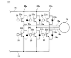
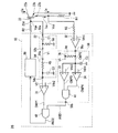
14 :モータ
16 :高電位配線
18 :低電位配線
19 :中間配線
22 :IGBT
23a:コレクタ
23b:エミッタ
23c:センスエミッタ
23d:ゲート
24 :pnダイオード
26 :ゲート制御回路
31−34 :コンパレータ
36 :定電圧配線
41−42 :AND回路
50 :制御回路
52 :微分回路
54 :フィルタ回路
56 :期間設定回路
Claims (1)
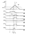
- IGBTを過電流から保護する保護回路であって、
前記IGBTのゲートを充放電する制御回路と、
前記ゲートが充電されているときに前記IGBTのゲート電圧の上昇率を検出するゲート電圧上昇率検出回路と、
前記IGBTに流れる電流を検出する電流検出回路、
を有し、
前記電流が第1基準値を超えたタイミングの後の一定期間内に前記上昇率が第2基準値を超えている場合に、前記制御回路が前記ゲートを放電する、
保護回路。
Priority Applications (1)
| Application Number | Priority Date | Filing Date | Title |
|---|---|---|---|
| JP2016059055A JP6711059B2 (ja) | 2016-03-23 | 2016-03-23 | 保護回路 |
Applications Claiming Priority (1)
| Application Number | Priority Date | Filing Date | Title |
|---|---|---|---|
| JP2016059055A JP6711059B2 (ja) | 2016-03-23 | 2016-03-23 | 保護回路 |
Publications (2)
| Publication Number | Publication Date |
|---|---|
| JP2017175780A true JP2017175780A (ja) | 2017-09-28 |
| JP6711059B2 JP6711059B2 (ja) | 2020-06-17 |
Family
ID=59972345
Family Applications (1)
| Application Number | Title | Priority Date | Filing Date |
|---|---|---|---|
| JP2016059055A Expired - Fee Related JP6711059B2 (ja) | 2016-03-23 | 2016-03-23 | 保護回路 |
Country Status (1)
| Country | Link |
|---|---|
| JP (1) | JP6711059B2 (ja) |
Cited By (2)
| Publication number | Priority date | Publication date | Assignee | Title |
|---|---|---|---|---|
| JP2020005132A (ja) * | 2018-06-28 | 2020-01-09 | 株式会社デンソー | 負荷駆動装置 |
| JP2020054088A (ja) * | 2018-09-26 | 2020-04-02 | 株式会社デンソー | スイッチの駆動回路 |
Citations (7)
| Publication number | Priority date | Publication date | Assignee | Title |
|---|---|---|---|---|
| JP2004119842A (ja) * | 2002-09-27 | 2004-04-15 | Mitsubishi Electric Corp | 電力用半導体素子の駆動回路 |
| JP2004266368A (ja) * | 2003-02-20 | 2004-09-24 | Hitachi Ltd | 半導体装置の駆動方法および装置 |
| JP2007306166A (ja) * | 2006-05-10 | 2007-11-22 | Toyota Motor Corp | 絶縁ゲート型半導体素子の駆動装置およびその方法 |
| WO2013008452A1 (ja) * | 2011-07-14 | 2013-01-17 | 富士電機株式会社 | 短絡保護回路 |
| JP2013123329A (ja) * | 2011-12-12 | 2013-06-20 | Toyota Motor Corp | スイッチング素子駆動回路及びそれを備える駆動装置 |
| JP2015023654A (ja) * | 2013-07-18 | 2015-02-02 | 株式会社デンソー | 半導体素子の電流検出装置 |
| EP2899886A1 (en) * | 2014-01-22 | 2015-07-29 | Hitachi, Ltd. | Semiconductor drive device and power conversion device using the same |
-
2016
- 2016-03-23 JP JP2016059055A patent/JP6711059B2/ja not_active Expired - Fee Related
Patent Citations (7)
| Publication number | Priority date | Publication date | Assignee | Title |
|---|---|---|---|---|
| JP2004119842A (ja) * | 2002-09-27 | 2004-04-15 | Mitsubishi Electric Corp | 電力用半導体素子の駆動回路 |
| JP2004266368A (ja) * | 2003-02-20 | 2004-09-24 | Hitachi Ltd | 半導体装置の駆動方法および装置 |
| JP2007306166A (ja) * | 2006-05-10 | 2007-11-22 | Toyota Motor Corp | 絶縁ゲート型半導体素子の駆動装置およびその方法 |
| WO2013008452A1 (ja) * | 2011-07-14 | 2013-01-17 | 富士電機株式会社 | 短絡保護回路 |
| JP2013123329A (ja) * | 2011-12-12 | 2013-06-20 | Toyota Motor Corp | スイッチング素子駆動回路及びそれを備える駆動装置 |
| JP2015023654A (ja) * | 2013-07-18 | 2015-02-02 | 株式会社デンソー | 半導体素子の電流検出装置 |
| EP2899886A1 (en) * | 2014-01-22 | 2015-07-29 | Hitachi, Ltd. | Semiconductor drive device and power conversion device using the same |
Cited By (4)
| Publication number | Priority date | Publication date | Assignee | Title |
|---|---|---|---|---|
| JP2020005132A (ja) * | 2018-06-28 | 2020-01-09 | 株式会社デンソー | 負荷駆動装置 |
| JP7124486B2 (ja) | 2018-06-28 | 2022-08-24 | 株式会社デンソー | 負荷駆動装置 |
| JP2020054088A (ja) * | 2018-09-26 | 2020-04-02 | 株式会社デンソー | スイッチの駆動回路 |
| JP7110871B2 (ja) | 2018-09-26 | 2022-08-02 | 株式会社デンソー | スイッチの駆動回路 |
Also Published As
| Publication number | Publication date |
|---|---|
| JP6711059B2 (ja) | 2020-06-17 |
Similar Documents
| Publication | Publication Date | Title |
|---|---|---|
| US9013850B2 (en) | Semiconductor device | |
| JP5500192B2 (ja) | スイッチング素子の駆動回路 | |
| JP5430608B2 (ja) | 半導体スイッチング素子駆動回路 | |
| US7368972B2 (en) | Power transistor control device | |
| US11095283B2 (en) | Drive control apparatus for driving a switching element including a sense element | |
| JP5057713B2 (ja) | スイッチング素子駆動回路 | |
| US7642817B2 (en) | Driver circuit for a semiconductor power switching element | |
| JP6939059B2 (ja) | 半導体素子の駆動装置 | |
| JP2003284318A (ja) | 電力用半導体素子の駆動回路 | |
| JP2005269446A (ja) | 電圧駆動型半導体素子用駆動回路 | |
| JP5541219B2 (ja) | 半導体スイッチング素子駆動装置 | |
| JP2012178951A (ja) | スイッチング素子の駆動回路 | |
| JPH04304015A (ja) | 電子スイッチ用短絡保護回路 | |
| JP2007306166A (ja) | 絶縁ゲート型半導体素子の駆動装置およびその方法 | |
| JP6711059B2 (ja) | 保護回路 | |
| JP6164183B2 (ja) | 電流制御回路 | |
| WO2018211840A1 (ja) | 制御装置及び半導体装置 | |
| JP2007267560A (ja) | 貫通電流制御装置を備えたインバータ | |
| CN114667681A (zh) | 栅极驱动电路 | |
| JP7326762B2 (ja) | 半導体モジュールおよび駆動回路 | |
| JP6622405B2 (ja) | インバータ駆動装置 | |
| WO2022255009A1 (ja) | ゲート駆動装置 | |
| WO2022255008A1 (ja) | ゲート駆動装置 | |
| WO2022153521A1 (ja) | 半導体電力変換装置 | |
| JP2017118790A (ja) | スイッチング回路 |
Legal Events
| Date | Code | Title | Description |
|---|---|---|---|
| A621 | Written request for application examination |
Free format text: JAPANESE INTERMEDIATE CODE: A621 Effective date: 20190306 |
|
| A977 | Report on retrieval |
Free format text: JAPANESE INTERMEDIATE CODE: A971007 Effective date: 20191225 |
|
| A131 | Notification of reasons for refusal |
Free format text: JAPANESE INTERMEDIATE CODE: A131 Effective date: 20200121 |
|
| A521 | Request for written amendment filed |
Free format text: JAPANESE INTERMEDIATE CODE: A523 Effective date: 20200304 |
|
| TRDD | Decision of grant or rejection written | ||
| A01 | Written decision to grant a patent or to grant a registration (utility model) |
Free format text: JAPANESE INTERMEDIATE CODE: A01 Effective date: 20200428 |
|
| A61 | First payment of annual fees (during grant procedure) |
Free format text: JAPANESE INTERMEDIATE CODE: A61 Effective date: 20200511 |
|
| R151 | Written notification of patent or utility model registration |
Ref document number: 6711059 Country of ref document: JP Free format text: JAPANESE INTERMEDIATE CODE: R151 |
|
| LAPS | Cancellation because of no payment of annual fees |