JP2016126170A - 液晶表示装置 - Google Patents
液晶表示装置 Download PDFInfo
- Publication number
- JP2016126170A JP2016126170A JP2014267007A JP2014267007A JP2016126170A JP 2016126170 A JP2016126170 A JP 2016126170A JP 2014267007 A JP2014267007 A JP 2014267007A JP 2014267007 A JP2014267007 A JP 2014267007A JP 2016126170 A JP2016126170 A JP 2016126170A
- Authority
- JP
- Japan
- Prior art keywords
- polarizing plate
- axis
- substrate
- liquid crystal
- electrode
- Prior art date
- Legal status (The legal status is an assumption and is not a legal conclusion. Google has not performed a legal analysis and makes no representation as to the accuracy of the status listed.)
- Pending
Links
Images


Classifications
-
- G—PHYSICS
- G02—OPTICS
- G02F—OPTICAL DEVICES OR ARRANGEMENTS FOR THE CONTROL OF LIGHT BY MODIFICATION OF THE OPTICAL PROPERTIES OF THE MEDIA OF THE ELEMENTS INVOLVED THEREIN; NON-LINEAR OPTICS; FREQUENCY-CHANGING OF LIGHT; OPTICAL LOGIC ELEMENTS; OPTICAL ANALOGUE/DIGITAL CONVERTERS
- G02F1/00—Devices or arrangements for the control of the intensity, colour, phase, polarisation or direction of light arriving from an independent light source, e.g. switching, gating or modulating; Non-linear optics
- G02F1/01—Devices or arrangements for the control of the intensity, colour, phase, polarisation or direction of light arriving from an independent light source, e.g. switching, gating or modulating; Non-linear optics for the control of the intensity, phase, polarisation or colour
- G02F1/13—Devices or arrangements for the control of the intensity, colour, phase, polarisation or direction of light arriving from an independent light source, e.g. switching, gating or modulating; Non-linear optics for the control of the intensity, phase, polarisation or colour based on liquid crystals, e.g. single liquid crystal display cells
- G02F1/133—Constructional arrangements; Operation of liquid crystal cells; Circuit arrangements
- G02F1/1333—Constructional arrangements; Manufacturing methods
- G02F1/1335—Structural association of cells with optical devices, e.g. polarisers or reflectors
- G02F1/13363—Birefringent elements, e.g. for optical compensation
-
- G—PHYSICS
- G02—OPTICS
- G02F—OPTICAL DEVICES OR ARRANGEMENTS FOR THE CONTROL OF LIGHT BY MODIFICATION OF THE OPTICAL PROPERTIES OF THE MEDIA OF THE ELEMENTS INVOLVED THEREIN; NON-LINEAR OPTICS; FREQUENCY-CHANGING OF LIGHT; OPTICAL LOGIC ELEMENTS; OPTICAL ANALOGUE/DIGITAL CONVERTERS
- G02F1/00—Devices or arrangements for the control of the intensity, colour, phase, polarisation or direction of light arriving from an independent light source, e.g. switching, gating or modulating; Non-linear optics
- G02F1/01—Devices or arrangements for the control of the intensity, colour, phase, polarisation or direction of light arriving from an independent light source, e.g. switching, gating or modulating; Non-linear optics for the control of the intensity, phase, polarisation or colour
- G02F1/13—Devices or arrangements for the control of the intensity, colour, phase, polarisation or direction of light arriving from an independent light source, e.g. switching, gating or modulating; Non-linear optics for the control of the intensity, phase, polarisation or colour based on liquid crystals, e.g. single liquid crystal display cells
- G02F1/133—Constructional arrangements; Operation of liquid crystal cells; Circuit arrangements
- G02F1/1333—Constructional arrangements; Manufacturing methods
- G02F1/1343—Electrodes
- G02F1/134309—Electrodes characterised by their geometrical arrangement
- G02F1/134372—Electrodes characterised by their geometrical arrangement for fringe field switching [FFS] where the common electrode is not patterned
-
- G—PHYSICS
- G02—OPTICS
- G02F—OPTICAL DEVICES OR ARRANGEMENTS FOR THE CONTROL OF LIGHT BY MODIFICATION OF THE OPTICAL PROPERTIES OF THE MEDIA OF THE ELEMENTS INVOLVED THEREIN; NON-LINEAR OPTICS; FREQUENCY-CHANGING OF LIGHT; OPTICAL LOGIC ELEMENTS; OPTICAL ANALOGUE/DIGITAL CONVERTERS
- G02F2413/00—Indexing scheme related to G02F1/13363, i.e. to birefringent elements, e.g. for optical compensation, characterised by the number, position, orientation or value of the compensation plates
- G02F2413/08—Indexing scheme related to G02F1/13363, i.e. to birefringent elements, e.g. for optical compensation, characterised by the number, position, orientation or value of the compensation plates with a particular optical axis orientation
Landscapes
- Physics & Mathematics (AREA)
- Nonlinear Science (AREA)
- Mathematical Physics (AREA)
- Chemical & Material Sciences (AREA)
- Crystallography & Structural Chemistry (AREA)
- General Physics & Mathematics (AREA)
- Optics & Photonics (AREA)
- Geometry (AREA)
- Liquid Crystal (AREA)
- Spectroscopy & Molecular Physics (AREA)
Abstract
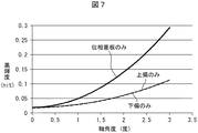
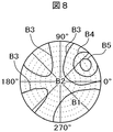
【解決手段】FFS方式の液晶表示装置において、第1の基板の第1の配向膜と第2の基板の第2の配向膜の配向軸1131は同じ方向であり、上偏光板250、下偏光板150、位相差板160のうちの少なくとも2つは、(1)上偏光板250の吸収軸は、配向軸1131と1度以上45度以下の角度を有すること、(2)下偏光板150の吸収軸は配向軸1131と91度以上135度以下、または89度以下で45度以上の角度を有すること、(3)位相差板160の延伸軸は、配向軸1131と1度以上45度以下の角度を有すること、のいずれかを満たすことを特徴とする液晶表示装置。
【選択図】図6
Description
前記位相差板の延伸軸は、前記配向軸と1度以上45度以下の角度を有すること、のいずれかを満たすことを特徴とする液晶表示装置。
Claims (7)
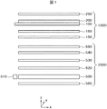
- 平面状の第1の電極の上に絶縁膜を介して櫛歯状の第2の電極が形成され、前記第1の電極の上に第1の配向膜が形成された第1の基板と、第2の配向膜が形成された第2の基板との間に液晶が挟持され、
前記第1の配向膜と前記第2の配向膜の配向軸は同じ方向であり、
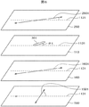
前記第2の基板の上には、上偏光板が配置し、前記第1の基板の下には下偏光板が配置し、前記下偏光板と前記第1の基板の間、または、前記上偏光板と前記第2の基板の間に位相差板が配置し、前記第1の電極と前記第2の電極の間に電圧を印加することによって画像を形成する液晶表示パネルを有する液晶表示装置であって、
前記上偏光板、前記下偏光板、前記位相差板のうちの少なくとも2つは、
前記上偏光板の吸収軸は、前記配向軸と1度以上45度以下の角度を有すること、
前記下偏光板の吸収軸は前記配向軸と91度以上135度以下、または89度以下で45度以上の角度を有すること、
前記位相差板の延伸軸は、前記配向軸と1度以上45度以下の角度を有すること、のいずれかを満たすことを特徴とする液晶表示装置。 - 平面状の第1の電極の上に絶縁膜を介して櫛歯状の第2の電極が形成され、前記第1の電極の上に第1の配向膜が形成された第1の基板と、第2の配向膜が形成された第2の基板との間に液晶が挟持され、
前記第1の配向膜と前記第2の配向膜の配向軸は同じ方向であり、
前記第2の基板の上には、上偏光板が配置し、前記第1の基板の下には下偏光板が配置し、前記下偏光板と前記第1の基板の間、または、前記上偏光板と前記第2の基板の間に位相差板が配置し、前記第1の電極と前記第2の電極の間に電圧を印加することによって画像を形成する液晶表示パネルを有する液晶表示装置であって、
前記上偏光板、前記下偏光板、前記位相差板のうちの少なくとも2つは、
前記上偏光板の吸収軸は、前記配向軸と91度以上135度以下、または89度以下で45度以上の角度を有すること、
前記下偏光板の吸収軸は前記配向軸と1度以上45度以下の角度を有すること、
前記位相差板の延伸軸は、前記配向軸と91度以上135度以下、または89度以下で45度以上の角度を有すること、のいずれかを満足することを特徴とする液晶表示装置。 - 前記位相差板は、前記第1の基板と前記下偏光板の間に配置していることを特徴とする請求項1または2に記載の液晶表示装置。
- 平面状の第1の電極の上に絶縁膜を介して櫛歯状の第2の電極が形成され、前記第1の電極の上に第1の配向膜が形成された第1の基板と、第2の配向膜が形成された第2の基板との間に液晶が挟持され、
前記第1の配向膜と前記第2の配向膜の配向軸は同じ方向であり、
前記第2の基板の上には、上偏光板が配置し、前記第1の基板の下には下偏光板が配置し、前記下偏光板と前記第1の基板の間、または、前記上偏光板と前記第2の基板の間に位相差板が配置し、前記第1の電極と前記第2の電極の間に電圧を印加することによって画像を形成する液晶表示パネルを有する液晶表示装置であって、
前記位相差板の延伸軸は、前記配向軸と一致しており、
前記上偏光板の吸収軸が前記配向軸となす角をxとし、前記下偏光板の吸収軸が前記配向軸となす角をyとしたとき、y=ax+90を満足し、
かつ、前記aの値は、0,81以上0.99以下であることを特徴とする液晶表示装置。 - 平面状の第1の電極の上に絶縁膜を介して櫛歯状の第2の電極が形成され、前記第1の電極の上に第1の配向膜が形成された第1の基板と、第2の配向膜が形成された第2の基板との間に液晶が挟持され、
前記第1の配向膜と前記第2の配向膜の配向軸は同じ方向であり、
前記第2の基板の上には、上偏光板が配置し、前記第1の基板の下には下偏光板が配置し、前記下偏光板と前記第1の基板の間、または、前記上偏光板と前記第2の基板の間に位相差板が配置し、前記第1の電極と前記第2の電極の間に電圧を印加することによって画像を形成する液晶表示パネルを有する液晶表示装置であって、
前記下偏光板の吸収軸は、前記配向軸と90度の角度をなしており、
前記上偏光板の吸収軸が前記配向軸となす角をxとし、前記位相差板の延伸軸が前記配向軸となす角をzとしたとき、z=bxを満足し、かつ、前記bは0.45以上で0.55以下であることを特徴とする液晶表示装置。 - 平面状の第1の電極の上に絶縁膜を介して櫛歯状の第2の電極が形成され、前記第1の電極の上に第1の配向膜が形成された第1の基板と、第2の配向膜が形成された第2の基板との間に液晶が挟持され、
前記第1の配向膜と前記第2の配向膜の配向軸は同じ方向であり、
前記第2の基板の上には、上偏光板が配置し、前記第1の基板の下には下偏光板が配置し、前記下偏光板と前記第1の基板の間、または、前記上偏光板と前記第2の基板の間に位相差板が配置し、前記第1の電極と前記第2の電極の間に電圧を印加することによって画像を形成する液晶表示パネルを有する液晶表示装置であって、
前記上偏光板の吸収軸は、前記配向軸と一致しており、
前記下偏光板の吸収軸が前記配向軸となす角をyとし、前記位相差板の延伸軸が前記配向軸となす角をzとしたとき、z=c(y−90)を満足し、かつ、前記cは0.45以上で0.55以下であることを特徴とする液晶表示装置。 - 前記位相差板は、前記第1の基板と前記下偏光板の間に配置していることを特徴とする請求項4乃至6のいずれか1項に記載の液晶表示装置。
Priority Applications (2)
| Application Number | Priority Date | Filing Date | Title |
|---|---|---|---|
| JP2014267007A JP2016126170A (ja) | 2014-12-29 | 2014-12-29 | 液晶表示装置 |
| US14/982,912 US9995965B2 (en) | 2014-12-29 | 2015-12-29 | Liquid crystal display device |
Applications Claiming Priority (1)
| Application Number | Priority Date | Filing Date | Title |
|---|---|---|---|
| JP2014267007A JP2016126170A (ja) | 2014-12-29 | 2014-12-29 | 液晶表示装置 |
Publications (2)
| Publication Number | Publication Date |
|---|---|
| JP2016126170A true JP2016126170A (ja) | 2016-07-11 |
| JP2016126170A5 JP2016126170A5 (ja) | 2017-11-02 |
Family
ID=56163983
Family Applications (1)
| Application Number | Title | Priority Date | Filing Date |
|---|---|---|---|
| JP2014267007A Pending JP2016126170A (ja) | 2014-12-29 | 2014-12-29 | 液晶表示装置 |
Country Status (2)
| Country | Link |
|---|---|
| US (1) | US9995965B2 (ja) |
| JP (1) | JP2016126170A (ja) |
Cited By (2)
| Publication number | Priority date | Publication date | Assignee | Title |
|---|---|---|---|---|
| WO2019123709A1 (ja) * | 2017-12-21 | 2019-06-27 | 三菱電機株式会社 | 液晶パネルおよびそれを備える液晶表示装置 |
| KR20200051270A (ko) * | 2018-11-05 | 2020-05-13 | 주식회사 엘지화학 | 광변조 소자 |
Citations (2)
| Publication number | Priority date | Publication date | Assignee | Title |
|---|---|---|---|---|
| JP2007328246A (ja) * | 2006-06-09 | 2007-12-20 | Fujifilm Corp | 液晶表示装置 |
| US20140300847A1 (en) * | 2013-03-29 | 2014-10-09 | University Of Central Florida Research Foundation , Inc. | Display apparatus |
Family Cites Families (5)
| Publication number | Priority date | Publication date | Assignee | Title |
|---|---|---|---|---|
| JPH06308497A (ja) | 1993-04-23 | 1994-11-04 | Fujitsu Ltd | 液晶表示装置 |
| JPH07253578A (ja) | 1994-03-16 | 1995-10-03 | Hitachi Ltd | 液晶表示装置 |
| TW200722842A (en) * | 2005-12-09 | 2007-06-16 | Innolux Display Corp | Liquid crystal display device |
| JP4337893B2 (ja) * | 2007-03-12 | 2009-09-30 | エプソンイメージングデバイス株式会社 | 液晶装置及び電子機器 |
| JP5380387B2 (ja) * | 2010-07-22 | 2014-01-08 | 株式会社ジャパンディスプレイ | 液晶表示装置 |
-
2014
- 2014-12-29 JP JP2014267007A patent/JP2016126170A/ja active Pending
-
2015
- 2015-12-29 US US14/982,912 patent/US9995965B2/en active Active
Patent Citations (2)
| Publication number | Priority date | Publication date | Assignee | Title |
|---|---|---|---|---|
| JP2007328246A (ja) * | 2006-06-09 | 2007-12-20 | Fujifilm Corp | 液晶表示装置 |
| US20140300847A1 (en) * | 2013-03-29 | 2014-10-09 | University Of Central Florida Research Foundation , Inc. | Display apparatus |
Cited By (3)
| Publication number | Priority date | Publication date | Assignee | Title |
|---|---|---|---|---|
| WO2019123709A1 (ja) * | 2017-12-21 | 2019-06-27 | 三菱電機株式会社 | 液晶パネルおよびそれを備える液晶表示装置 |
| KR20200051270A (ko) * | 2018-11-05 | 2020-05-13 | 주식회사 엘지화학 | 광변조 소자 |
| KR102290713B1 (ko) * | 2018-11-05 | 2021-08-18 | 주식회사 엘지화학 | 광변조 소자 |
Also Published As
| Publication number | Publication date |
|---|---|
| US20160187722A1 (en) | 2016-06-30 |
| US9995965B2 (en) | 2018-06-12 |
Similar Documents
| Publication | Publication Date | Title |
|---|---|---|
| JP5156506B2 (ja) | 液晶表示装置 | |
| CN103529608B (zh) | 用于液晶显示设备的阵列基板及其制造方法 | |
| US9235083B2 (en) | Liquid crystal display device | |
| WO2018131533A1 (ja) | 液晶表示装置 | |
| JP2014215348A (ja) | 液晶パネル | |
| US9638966B2 (en) | Liquid crystal display device | |
| JP4541129B2 (ja) | 液晶表示装置 | |
| US10133132B2 (en) | Liquid crystal display device | |
| WO2013100088A1 (ja) | 液晶表示装置 | |
| JP2008033254A (ja) | 液晶ディスプレイパネル | |
| JP4551246B2 (ja) | 液晶表示装置 | |
| US20060028604A1 (en) | Liquid crystal display device | |
| CN104656322B (zh) | 液晶显示装置和三维显示装置 | |
| WO2015043055A1 (zh) | 阵列基板及其制作方法、液晶面板及显示装置 | |
| JP2016126170A (ja) | 液晶表示装置 | |
| JP2007163722A (ja) | 液晶装置とその製造方法、位相差板、及び電子機器 | |
| US8284359B2 (en) | Liquid crystal panel and liquid crystal display device | |
| JP6415856B2 (ja) | 液晶表示装置 | |
| US20130329177A1 (en) | Liquid-crystal display | |
| JP2001242442A (ja) | 液晶表示装置 | |
| JP2009276435A (ja) | 液晶表示装置 | |
| JP2016148760A (ja) | 液晶表示装置 | |
| JP2008241959A (ja) | 液晶表示装置 | |
| JP4636626B2 (ja) | 液晶表示素子 | |
| WO2019159552A1 (ja) | 液晶表示装置 |
Legal Events
| Date | Code | Title | Description |
|---|---|---|---|
| A521 | Request for written amendment filed |
Free format text: JAPANESE INTERMEDIATE CODE: A523 Effective date: 20170914 |
|
| A621 | Written request for application examination |
Free format text: JAPANESE INTERMEDIATE CODE: A621 Effective date: 20170914 |
|
| A131 | Notification of reasons for refusal |
Free format text: JAPANESE INTERMEDIATE CODE: A131 Effective date: 20180424 |
|
| A977 | Report on retrieval |
Free format text: JAPANESE INTERMEDIATE CODE: A971007 Effective date: 20180425 |
|
| A02 | Decision of refusal |
Free format text: JAPANESE INTERMEDIATE CODE: A02 Effective date: 20181023 |