JP2016119300A - 基準マークに基づく相関顕微鏡法 - Google Patents
基準マークに基づく相関顕微鏡法 Download PDFInfo
- Publication number
- JP2016119300A JP2016119300A JP2015243742A JP2015243742A JP2016119300A JP 2016119300 A JP2016119300 A JP 2016119300A JP 2015243742 A JP2015243742 A JP 2015243742A JP 2015243742 A JP2015243742 A JP 2015243742A JP 2016119300 A JP2016119300 A JP 2016119300A
- Authority
- JP
- Japan
- Prior art keywords
- sample volume
- charged particle
- imaging
- images
- reference mark
- Prior art date
- Legal status (The legal status is an assumption and is not a legal conclusion. Google has not performed a legal analysis and makes no representation as to the accuracy of the status listed.)
- Pending
Links
- 238000000386 microscopy Methods 0.000 title claims description 19
- 238000000034 method Methods 0.000 claims abstract description 118
- 239000002245 particle Substances 0.000 claims abstract description 89
- 230000003287 optical effect Effects 0.000 claims abstract description 69
- 238000003384 imaging method Methods 0.000 claims abstract description 67
- 239000003550 marker Substances 0.000 claims description 25
- 238000010884 ion-beam technique Methods 0.000 claims description 16
- 230000008859 change Effects 0.000 claims description 15
- 239000000463 material Substances 0.000 claims description 13
- 238000012634 optical imaging Methods 0.000 claims description 12
- 239000000758 substrate Substances 0.000 claims description 12
- 238000003860 storage Methods 0.000 claims description 11
- 238000012937 correction Methods 0.000 claims description 10
- 239000002105 nanoparticle Substances 0.000 claims description 7
- 102000004169 proteins and genes Human genes 0.000 claims description 5
- 108090000623 proteins and genes Proteins 0.000 claims description 5
- 238000003801 milling Methods 0.000 claims description 4
- 239000002096 quantum dot Substances 0.000 claims description 4
- 238000001000 micrograph Methods 0.000 claims description 2
- 238000004626 scanning electron microscopy Methods 0.000 claims description 2
- 238000003702 image correction Methods 0.000 claims 2
- 239000000975 dye Substances 0.000 abstract description 35
- 230000008569 process Effects 0.000 abstract description 21
- 239000007850 fluorescent dye Substances 0.000 abstract description 6
- 239000002077 nanosphere Substances 0.000 abstract description 6
- 239000004793 Polystyrene Substances 0.000 abstract description 4
- 229920002223 polystyrene Polymers 0.000 abstract description 4
- 230000004075 alteration Effects 0.000 abstract 1
- 239000000523 sample Substances 0.000 description 149
- 238000010894 electron beam technology Methods 0.000 description 14
- 238000001493 electron microscopy Methods 0.000 description 10
- 238000002360 preparation method Methods 0.000 description 8
- 230000004807 localization Effects 0.000 description 7
- 238000000399 optical microscopy Methods 0.000 description 7
- 238000010186 staining Methods 0.000 description 7
- 239000012472 biological sample Substances 0.000 description 6
- 230000009977 dual effect Effects 0.000 description 5
- 230000006870 function Effects 0.000 description 5
- 239000002609 medium Substances 0.000 description 5
- 238000000576 coating method Methods 0.000 description 4
- 238000004590 computer program Methods 0.000 description 4
- 238000010586 diagram Methods 0.000 description 4
- 230000005284 excitation Effects 0.000 description 4
- 125000000524 functional group Chemical group 0.000 description 4
- PCHJSUWPFVWCPO-UHFFFAOYSA-N gold Chemical compound [Au] PCHJSUWPFVWCPO-UHFFFAOYSA-N 0.000 description 4
- 229910001385 heavy metal Inorganic materials 0.000 description 4
- 238000012545 processing Methods 0.000 description 4
- 238000004422 calculation algorithm Methods 0.000 description 3
- 210000004027 cell Anatomy 0.000 description 3
- 230000001413 cellular effect Effects 0.000 description 3
- 210000003850 cellular structure Anatomy 0.000 description 3
- 239000011248 coating agent Substances 0.000 description 3
- 230000002596 correlated effect Effects 0.000 description 3
- 238000000635 electron micrograph Methods 0.000 description 3
- 238000004519 manufacturing process Methods 0.000 description 3
- 239000000203 mixture Substances 0.000 description 3
- 239000011347 resin Substances 0.000 description 3
- 229920005989 resin Polymers 0.000 description 3
- LFQSCWFLJHTTHZ-UHFFFAOYSA-N Ethanol Chemical compound CCO LFQSCWFLJHTTHZ-UHFFFAOYSA-N 0.000 description 2
- VYPSYNLAJGMNEJ-UHFFFAOYSA-N Silicium dioxide Chemical compound O=[Si]=O VYPSYNLAJGMNEJ-UHFFFAOYSA-N 0.000 description 2
- 238000004624 confocal microscopy Methods 0.000 description 2
- 239000006059 cover glass Substances 0.000 description 2
- 230000007812 deficiency Effects 0.000 description 2
- 230000018044 dehydration Effects 0.000 description 2
- 238000006297 dehydration reaction Methods 0.000 description 2
- 238000002059 diagnostic imaging Methods 0.000 description 2
- 102000034287 fluorescent proteins Human genes 0.000 description 2
- 108091006047 fluorescent proteins Proteins 0.000 description 2
- 229910000489 osmium tetroxide Inorganic materials 0.000 description 2
- 239000012285 osmium tetroxide Substances 0.000 description 2
- 239000000126 substance Substances 0.000 description 2
- 238000003325 tomography Methods 0.000 description 2
- 238000004627 transmission electron microscopy Methods 0.000 description 2
- 239000004925 Acrylic resin Substances 0.000 description 1
- 229920000178 Acrylic resin Polymers 0.000 description 1
- 229920000936 Agarose Polymers 0.000 description 1
- 239000012103 Alexa Fluor 488 Substances 0.000 description 1
- OKTJSMMVPCPJKN-UHFFFAOYSA-N Carbon Chemical compound [C] OKTJSMMVPCPJKN-UHFFFAOYSA-N 0.000 description 1
- COQLPRJCUIATTQ-UHFFFAOYSA-N Uranyl acetate Chemical compound O.O.O=[U]=O.CC(O)=O.CC(O)=O COQLPRJCUIATTQ-UHFFFAOYSA-N 0.000 description 1
- 239000011543 agarose gel Substances 0.000 description 1
- 150000001412 amines Chemical class 0.000 description 1
- 238000004873 anchoring Methods 0.000 description 1
- 239000011324 bead Substances 0.000 description 1
- 230000031018 biological processes and functions Effects 0.000 description 1
- 238000001574 biopsy Methods 0.000 description 1
- 238000004364 calculation method Methods 0.000 description 1
- 239000002134 carbon nanofiber Substances 0.000 description 1
- 239000002041 carbon nanotube Substances 0.000 description 1
- 229910021393 carbon nanotube Inorganic materials 0.000 description 1
- 239000003086 colorant Substances 0.000 description 1
- 238000010226 confocal imaging Methods 0.000 description 1
- 238000000942 confocal micrograph Methods 0.000 description 1
- 230000000875 corresponding effect Effects 0.000 description 1
- 238000011161 development Methods 0.000 description 1
- 230000018109 developmental process Effects 0.000 description 1
- ZBCBWPMODOFKDW-UHFFFAOYSA-N diethanolamine Chemical group OCCNCCO ZBCBWPMODOFKDW-UHFFFAOYSA-N 0.000 description 1
- 239000006185 dispersion Substances 0.000 description 1
- 238000006073 displacement reaction Methods 0.000 description 1
- 238000009826 distribution Methods 0.000 description 1
- 238000005553 drilling Methods 0.000 description 1
- 238000003708 edge detection Methods 0.000 description 1
- 238000000295 emission spectrum Methods 0.000 description 1
- 238000005516 engineering process Methods 0.000 description 1
- 238000002073 fluorescence micrograph Methods 0.000 description 1
- 238000000799 fluorescence microscopy Methods 0.000 description 1
- 238000002189 fluorescence spectrum Methods 0.000 description 1
- 239000000499 gel Substances 0.000 description 1
- 238000005286 illumination Methods 0.000 description 1
- 230000002779 inactivation Effects 0.000 description 1
- 229910052500 inorganic mineral Inorganic materials 0.000 description 1
- 238000003780 insertion Methods 0.000 description 1
- 230000037431 insertion Effects 0.000 description 1
- 238000001886 ion microscopy Methods 0.000 description 1
- 238000002372 labelling Methods 0.000 description 1
- 239000004816 latex Substances 0.000 description 1
- 229920000126 latex Polymers 0.000 description 1
- 230000033001 locomotion Effects 0.000 description 1
- 239000011159 matrix material Substances 0.000 description 1
- 238000005259 measurement Methods 0.000 description 1
- 239000002082 metal nanoparticle Substances 0.000 description 1
- VNWKTOKETHGBQD-UHFFFAOYSA-N methane Chemical class C VNWKTOKETHGBQD-UHFFFAOYSA-N 0.000 description 1
- 239000011707 mineral Substances 0.000 description 1
- 230000004048 modification Effects 0.000 description 1
- 238000012986 modification Methods 0.000 description 1
- 239000002073 nanorod Substances 0.000 description 1
- 230000000149 penetrating effect Effects 0.000 description 1
- 239000000088 plastic resin Substances 0.000 description 1
- 239000013630 prepared media Substances 0.000 description 1
- 125000002924 primary amino group Chemical group [H]N([H])* 0.000 description 1
- 230000006798 recombination Effects 0.000 description 1
- 238000005215 recombination Methods 0.000 description 1
- 238000001878 scanning electron micrograph Methods 0.000 description 1
- 238000000027 scanning ion microscopy Methods 0.000 description 1
- 238000001350 scanning transmission electron microscopy Methods 0.000 description 1
- 239000000377 silicon dioxide Substances 0.000 description 1
- 239000002904 solvent Substances 0.000 description 1
- 238000006467 substitution reaction Methods 0.000 description 1
- -1 sulfodichlorophenol ester Chemical class 0.000 description 1
- 238000010869 super-resolution microscopy Methods 0.000 description 1
- 238000012360 testing method Methods 0.000 description 1
- 229930195735 unsaturated hydrocarbon Natural products 0.000 description 1
- 230000000007 visual effect Effects 0.000 description 1
Images


Classifications
-
- G—PHYSICS
- G01—MEASURING; TESTING
- G01N—INVESTIGATING OR ANALYSING MATERIALS BY DETERMINING THEIR CHEMICAL OR PHYSICAL PROPERTIES
- G01N21/00—Investigating or analysing materials by the use of optical means, i.e. using sub-millimetre waves, infrared, visible or ultraviolet light
- G01N21/62—Systems in which the material investigated is excited whereby it emits light or causes a change in wavelength of the incident light
- G01N21/63—Systems in which the material investigated is excited whereby it emits light or causes a change in wavelength of the incident light optically excited
- G01N21/64—Fluorescence; Phosphorescence
- G01N21/6486—Measuring fluorescence of biological material, e.g. DNA, RNA, cells
-
- H—ELECTRICITY
- H01—ELECTRIC ELEMENTS
- H01J—ELECTRIC DISCHARGE TUBES OR DISCHARGE LAMPS
- H01J37/00—Discharge tubes with provision for introducing objects or material to be exposed to the discharge, e.g. for the purpose of examination or processing thereof
- H01J37/02—Details
- H01J37/22—Optical or photographic arrangements associated with the tube
- H01J37/222—Image processing arrangements associated with the tube
-
- G—PHYSICS
- G01—MEASURING; TESTING
- G01N—INVESTIGATING OR ANALYSING MATERIALS BY DETERMINING THEIR CHEMICAL OR PHYSICAL PROPERTIES
- G01N21/00—Investigating or analysing materials by the use of optical means, i.e. using sub-millimetre waves, infrared, visible or ultraviolet light
- G01N21/62—Systems in which the material investigated is excited whereby it emits light or causes a change in wavelength of the incident light
- G01N21/63—Systems in which the material investigated is excited whereby it emits light or causes a change in wavelength of the incident light optically excited
- G01N21/64—Fluorescence; Phosphorescence
- G01N21/6428—Measuring fluorescence of fluorescent products of reactions or of fluorochrome labelled reactive substances, e.g. measuring quenching effects, using measuring "optrodes"
-
- G—PHYSICS
- G01—MEASURING; TESTING
- G01N—INVESTIGATING OR ANALYSING MATERIALS BY DETERMINING THEIR CHEMICAL OR PHYSICAL PROPERTIES
- G01N21/00—Investigating or analysing materials by the use of optical means, i.e. using sub-millimetre waves, infrared, visible or ultraviolet light
- G01N21/62—Systems in which the material investigated is excited whereby it emits light or causes a change in wavelength of the incident light
- G01N21/63—Systems in which the material investigated is excited whereby it emits light or causes a change in wavelength of the incident light optically excited
- G01N21/64—Fluorescence; Phosphorescence
- G01N21/645—Specially adapted constructive features of fluorimeters
- G01N21/6456—Spatial resolved fluorescence measurements; Imaging
- G01N21/6458—Fluorescence microscopy
-
- G—PHYSICS
- G01—MEASURING; TESTING
- G01N—INVESTIGATING OR ANALYSING MATERIALS BY DETERMINING THEIR CHEMICAL OR PHYSICAL PROPERTIES
- G01N23/00—Investigating or analysing materials by the use of wave or particle radiation, e.g. X-rays or neutrons, not covered by groups G01N3/00 – G01N17/00, G01N21/00 or G01N22/00
- G01N23/22—Investigating or analysing materials by the use of wave or particle radiation, e.g. X-rays or neutrons, not covered by groups G01N3/00 – G01N17/00, G01N21/00 or G01N22/00 by measuring secondary emission from the material
- G01N23/223—Investigating or analysing materials by the use of wave or particle radiation, e.g. X-rays or neutrons, not covered by groups G01N3/00 – G01N17/00, G01N21/00 or G01N22/00 by measuring secondary emission from the material by irradiating the sample with X-rays or gamma-rays and by measuring X-ray fluorescence
-
- G—PHYSICS
- G02—OPTICS
- G02B—OPTICAL ELEMENTS, SYSTEMS OR APPARATUS
- G02B21/00—Microscopes
- G02B21/0004—Microscopes specially adapted for specific applications
- G02B21/002—Scanning microscopes
- G02B21/0024—Confocal scanning microscopes (CSOMs) or confocal "macroscopes"; Accessories which are not restricted to use with CSOMs, e.g. sample holders
- G02B21/0032—Optical details of illumination, e.g. light-sources, pinholes, beam splitters, slits, fibers
-
- G—PHYSICS
- G02—OPTICS
- G02B—OPTICAL ELEMENTS, SYSTEMS OR APPARATUS
- G02B21/00—Microscopes
- G02B21/0004—Microscopes specially adapted for specific applications
- G02B21/002—Scanning microscopes
- G02B21/0024—Confocal scanning microscopes (CSOMs) or confocal "macroscopes"; Accessories which are not restricted to use with CSOMs, e.g. sample holders
- G02B21/0052—Optical details of the image generation
- G02B21/0076—Optical details of the image generation arrangements using fluorescence or luminescence
-
- G—PHYSICS
- G02—OPTICS
- G02B—OPTICAL ELEMENTS, SYSTEMS OR APPARATUS
- G02B21/00—Microscopes
- G02B21/0004—Microscopes specially adapted for specific applications
- G02B21/002—Scanning microscopes
- G02B21/0024—Confocal scanning microscopes (CSOMs) or confocal "macroscopes"; Accessories which are not restricted to use with CSOMs, e.g. sample holders
- G02B21/008—Details of detection or image processing, including general computer control
-
- G—PHYSICS
- G02—OPTICS
- G02B—OPTICAL ELEMENTS, SYSTEMS OR APPARATUS
- G02B21/00—Microscopes
- G02B21/16—Microscopes adapted for ultraviolet illumination ; Fluorescence microscopes
-
- G—PHYSICS
- G02—OPTICS
- G02B—OPTICAL ELEMENTS, SYSTEMS OR APPARATUS
- G02B21/00—Microscopes
- G02B21/36—Microscopes arranged for photographic purposes or projection purposes or digital imaging or video purposes including associated control and data processing arrangements
- G02B21/365—Control or image processing arrangements for digital or video microscopes
-
- H—ELECTRICITY
- H01—ELECTRIC ELEMENTS
- H01J—ELECTRIC DISCHARGE TUBES OR DISCHARGE LAMPS
- H01J37/00—Discharge tubes with provision for introducing objects or material to be exposed to the discharge, e.g. for the purpose of examination or processing thereof
- H01J37/26—Electron or ion microscopes; Electron or ion diffraction tubes
-
- G—PHYSICS
- G01—MEASURING; TESTING
- G01N—INVESTIGATING OR ANALYSING MATERIALS BY DETERMINING THEIR CHEMICAL OR PHYSICAL PROPERTIES
- G01N21/00—Investigating or analysing materials by the use of optical means, i.e. using sub-millimetre waves, infrared, visible or ultraviolet light
- G01N21/62—Systems in which the material investigated is excited whereby it emits light or causes a change in wavelength of the incident light
- G01N21/63—Systems in which the material investigated is excited whereby it emits light or causes a change in wavelength of the incident light optically excited
- G01N21/64—Fluorescence; Phosphorescence
- G01N21/6428—Measuring fluorescence of fluorescent products of reactions or of fluorochrome labelled reactive substances, e.g. measuring quenching effects, using measuring "optrodes"
- G01N2021/6439—Measuring fluorescence of fluorescent products of reactions or of fluorochrome labelled reactive substances, e.g. measuring quenching effects, using measuring "optrodes" with indicators, stains, dyes, tags, labels, marks
-
- H—ELECTRICITY
- H01—ELECTRIC ELEMENTS
- H01J—ELECTRIC DISCHARGE TUBES OR DISCHARGE LAMPS
- H01J2237/00—Discharge tubes exposing object to beam, e.g. for analysis treatment, etching, imaging
- H01J2237/22—Treatment of data
- H01J2237/221—Image processing
-
- H—ELECTRICITY
- H01—ELECTRIC ELEMENTS
- H01J—ELECTRIC DISCHARGE TUBES OR DISCHARGE LAMPS
- H01J2237/00—Discharge tubes exposing object to beam, e.g. for analysis treatment, etching, imaging
- H01J2237/245—Detection characterised by the variable being measured
- H01J2237/24571—Measurements of non-electric or non-magnetic variables
- H01J2237/24578—Spatial variables, e.g. position, distance
-
- H—ELECTRICITY
- H01—ELECTRIC ELEMENTS
- H01J—ELECTRIC DISCHARGE TUBES OR DISCHARGE LAMPS
- H01J2237/00—Discharge tubes exposing object to beam, e.g. for analysis treatment, etching, imaging
- H01J2237/26—Electron or ion microscopes
- H01J2237/2611—Stereoscopic measurements and/or imaging
Abstract
Description
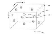
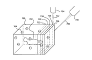
102 関心の領域
103 固定材
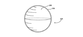
104 球
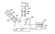
602 電子ビーム・カラム
604 電子源
610 電子ビーム
612 試料
614 試料ステージ
616 集束イオン・ビーム・カラム
Claims (33)
- 光学画像および荷電粒子画像を利用した試料体積中の関心の領域の位置の3次元相関の方法であって、
試料体積を含む試料を提供することであり、前記試料体積が、関心の領域を包含し、前記試料体積中に分布した基準マークとを含み、前記基準マークが、前記試料体積の光学画像中と荷電粒子画像中の両方で識別可能であることと、
前記試料体積を光学システムを使用して画像化することと、
前記試料体積を荷電粒子ビームを使用して画像化することと、
前記光学画像中と前記荷電粒子ビーム画像中の両方で識別された前記基準マークの位置を使用して、前記試料体積中の関心の領域の位置を相関させることと
を含む方法。 - 前記基準マークが既知の3次元形状を有し、前記基準マークが表面にマーカを含み、しかし内部には含まない、請求項1に記載の方法。
- 前記試料体積中の関心の領域の位置を相関させることが、前記試料体積の全体にわたって分布した前記基準マークのうちの少なくともいくつかの基準マークの3次元位置を、1つまたは複数の光学画像を使用して決定すること、および前記試料体積中に分布した前記基準マークの3次元位置を、1つまたは複数の荷電粒子画像を使用して決定することを含む、請求項1または2に記載の方法。
- 前記試料体積を前記光学システムを使用して画像化することと、前記試料体積を前記荷電粒子ビームを使用して画像化することの間で、前記試料体積の形状が変化し、前記試料体積中の関心の領域の位置を相関させることが、前記荷電粒子ビーム画像の画素を再配分して、前記光学画像中の前記基準マークの3次元位置が、前記荷電粒子ビーム画像中の前記基準マークの3次元位置と一致するようにすることを含む、請求項1から3のいずれか一項に記載の方法。
- 前記試料体積を前記光学システムを使用して画像化することと、前記試料体積を前記荷電粒子ビームを使用して画像化することの間で、前記基準マークの形状が変化し、前記試料体積中の関心の領域の位置を相関させることが、前記基準マークの形状の前記変化を使用することを含む、請求項1から4のいずれか一項に記載の方法。
- 前記基準マークが既知の3次元形状を有し、前記基準マークが表面にマーカを含み、しかし内部には含まない、請求項1から5のいずれか一項に記載の方法。
- 前記試料体積中に分布した前記基準マークが蛍光球を含み、前記蛍光球が、前記球の表面に存在し前記球の内部には浸透しない染料を含む、請求項1から6のいずれか一項に記載の方法。
- 近くの蛍光マーカから実質的に干渉されることなくそれぞれの基準マークを個別に画像化することができる十分に低い濃度で、前記基準マークが前記試料体積中に分布している、請求項1から7のいずれか一項に記載の方法。
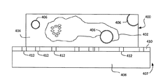
- 前記試料体積と基板との境界面のX−Y平面内に基準マークの平面層をさらに含み、前記基準マークが、前記試料体積の全体にわたって分布した前記基準マークと区別できる、請求項1から8のいずれか一項に記載の方法。
- 前記試料体積を光学システムを使用して画像化することが、3次元超解像画像化を含む、請求項1から9のいずれか一項に記載の方法。
- 超解像画像化が光活性化局在性顕微鏡法を含む、請求項10に記載の方法。
- 物体の3次元位置を、前記荷電粒子ビーム・システムを使用して、逐次画像化および材料除去サイクルによって得る、請求項1から11のいずれか一項に記載の方法。
- 画像化が、走査電子顕微鏡画像を得ることを含み、材料除去が、集束イオン・ビームを用いたミリングを含む、請求項12に記載の方法。
- 前記基準マークが蛍光ナノ粒子を含む、請求項1から13のいずれか一項に記載の方法。
- 前記ナノ粒子が、染料によって機能化された球である、請求項14に記載の方法。
- 前記染料によって機能化された球が、前記球の表面に存在し前記球の内部には浸透しない染料を含む、請求項15に記載の方法。
- 前記染料が、光活性化可能な染料またはタンパク質である、請求項15または16に記載の方法。
- 前記ナノ粒子が量子ドットである、請求項14に記載の方法。
- 前記基準マークの3次元位置を、1つもしくは複数の荷電粒子画像または1つもしくは複数の光学画像を使用して決定することが、前記基準マークの3次元形状を決定することをさらに含む、請求項2から18のいずれか一項に記載の方法。
- 前記光学画像中と前記荷電粒子ビーム画像中の両方で識別された前記基準マークの位置を使用することが、前記基準マークの形状の変化を使用することをさらに含む、請求項14に記載の方法。
- 試料体積中の空間的変化を補正する方法であって、
試料体積を提供することであり、前記試料体積が、前記試料体積の全体にわたって分散した基準マークを含むことと、
前記試料体積を光学システムを使用して画像化することと、
集められた1つまたは複数の前記光学画像を使用して、前記試料体積中に分布した前記基準マークの3次元位置を決定することと、
前記試料を荷電粒子ビーム・システムに導入することと、
前記試料を荷電粒子ビームを使用して画像化することと、
集められた1つまたは複数の前記荷電粒子ビーム画像を使用して、前記試料体積中に分布した前記基準マークの3次元位置を決定することと、
前記1つまたは複数の光学画像中の前記基準マークの位置を、前記1つまたは複数の荷電粒子ビーム画像中の前記基準マークの位置と比較することと、
前記1つまたは複数の光学画像と1つまたは複数の荷電粒子画像の間の基準マークの位置の差を計算することと、
前記試料体積に対する空間的変化を考慮するために、前記1つまたは複数の光学画像あるいは前記1つまたは複数の荷電粒子画像に補正を適用することと
を含む方法。 - 前記基準マークの3次元位置を決定することが、前記基準マークの3次元形状を決定することをさらに含む、請求項21に記載の方法。
- 補正を適用した後に、前記1つまたは複数の光学画像に前記1つまたは複数の荷電粒子画像をオーバレイするスことさらに含む、請求項21または22に記載の方法。
- 光学画像化が3次元超解像画像化を含む、請求項21から23のいずれか一項に記載の方法。
- 荷電粒子画像化が、逐次画像化および材料除去サイクルによる一連の画像を含み、前記一連の逐次画像を処理して、前記試料体積の3次元表現にすることができる、請求項21から24のいずれか一項に記載の方法。
- 前記1つまたは複数の光学画像中の基準マークと前記1つまたは複数の荷電粒子画像中の基準マークの間の相対距離を比較することによって、基準マークの位置の差を決定する、請求項21から25のいずれか一項に記載の方法。
- 選択された基準マークの相対形状を光学画像化と荷電粒子画像化の間で比較することによって、前記基準マークの形状の変化を決定する、請求項21から26のいずれか一項に記載の方法。
- 光学画像化と荷電粒子画像化の間の前記基準マークの形状の任意の変化を計算し、この変化を使用して、前記1つもしくは複数の光学画像または前記1つまたは複数の荷電粒子画像に補正を適用する、請求項21から27のいずれか一項に記載の方法。
- 試料体積中の空間的変化の画像補正のための装置であって、
荷電粒子画像化システムと、
光学画像化システムと、
試料体積の全体にわたって分布した基準マークを含む前記試料体積と、
不揮発性記憶装置に接続された制御装置と
を備え、
前記記憶装置が、以下の各動作:
前記試料体積を光学システムを使用して画像化すること、
集められた1つまたは複数の前記光学画像を使用して、前記試料体積の全体にわたって分布した前記基準マークの3次元位置を決定すること、
前記試料体積を荷電粒子ビームを使用して画像化すること、
集められた1つまたは複数の前記荷電粒子ビーム画像を使用して、前記試料体積の全体にわたって分布した前記基準マークの3次元位置を決定すること、
前記1つまたは複数の光学画像中の前記基準マークの位置を、前記1つまたは複数の荷電粒子ビーム画像中の前記基準マークの位置と比較すること、
前記1つまたは複数の光学画像と前記1つまたは複数の荷電粒子画像の間の基準マークの位置の差を計算すること、および
前記試料体積に対する空間的変化を考慮するために、前記1つまたは複数の光学画像あるいは前記1つまたは複数の荷電粒子画像に補正を適用すること
を実行するよう前記制御装置に命令する命令を記憶した、試料体積中の空間的変化の画像補正のための装置。 - 前記基準マークの3次元位置を決定することが、前記基準マークの3次元形状を決定することをさらに含む、請求項29に記載の装置。
- 光学画像化が3次元超解像画像化を含み、荷電粒子画像化が走査電子顕微鏡法を含む、請求項29または30に記載の装置。
- 前記1つまたは複数の光学画像中の基準マークと前記1つまたは複数の荷電粒子画像中の基準マークの間の相対距離を比較することによって、基準マークの位置と形状のうちの一方または両方の差を決定する、請求項29から31のいずれか一項に記載の装置。
- 基準マークの位置と形状のうちの一方または両方の差が、前記試料の形状に対する物理的変化によって生じる、請求項29または32に記載の装置。
Applications Claiming Priority (2)
| Application Number | Priority Date | Filing Date | Title |
|---|---|---|---|
| US14/579,056 | 2014-12-22 | ||
| US14/579,056 US9368321B1 (en) | 2014-12-22 | 2014-12-22 | Fiducial-based correlative microscopy |
Publications (2)
| Publication Number | Publication Date |
|---|---|
| JP2016119300A true JP2016119300A (ja) | 2016-06-30 |
| JP2016119300A5 JP2016119300A5 (ja) | 2019-01-31 |
Family
ID=54849802
Family Applications (1)
| Application Number | Title | Priority Date | Filing Date |
|---|---|---|---|
| JP2015243742A Pending JP2016119300A (ja) | 2014-12-22 | 2015-12-15 | 基準マークに基づく相関顕微鏡法 |
Country Status (4)
| Country | Link |
|---|---|
| US (1) | US9368321B1 (ja) |
| EP (1) | EP3037862A1 (ja) |
| JP (1) | JP2016119300A (ja) |
| CN (1) | CN105717078A (ja) |
Cited By (4)
| Publication number | Priority date | Publication date | Assignee | Title |
|---|---|---|---|---|
| WO2020080508A1 (ja) * | 2018-10-19 | 2020-04-23 | 株式会社日立ハイテクノロジーズ | アライメントシステム及び位置合わせ用シール |
| JP2020514822A (ja) * | 2017-03-17 | 2020-05-21 | ユナイテッド キングダム リサーチ アンド イノベーション | 超解像顕微鏡法 |
| JP2020136053A (ja) * | 2019-02-19 | 2020-08-31 | 日本電子株式会社 | 観察方法、画像処理装置、および電子顕微鏡 |
| US11676794B2 (en) | 2017-03-17 | 2023-06-13 | United Kingdom Research And Innovation | Super-resolution microscopy |
Families Citing this family (10)
| Publication number | Priority date | Publication date | Assignee | Title |
|---|---|---|---|---|
| US11896944B2 (en) | 2017-02-01 | 2024-02-13 | Illumina, Inc. | System and method with fiducials responding to multiple excitation frequencies |
| GB201701689D0 (en) | 2017-02-01 | 2017-03-15 | Illumia Inc | System and method with fiducials of non-closed shapes |
| GB201701686D0 (en) | 2017-02-01 | 2017-03-15 | Illunina Inc | System & method with fiducials having offset layouts |
| GB201701691D0 (en) * | 2017-02-01 | 2017-03-15 | Illumina Inc | System and method with reflective fiducials |
| GB201701688D0 (en) * | 2017-02-01 | 2017-03-15 | Illumia Inc | System and method with fiducials in non-recliner layouts |
| US10252350B1 (en) | 2018-06-17 | 2019-04-09 | Arevo, Inc. | Fiducial marks for articles of manufacture with non-trivial dimensional variations |
| CN111239085B (zh) * | 2019-03-06 | 2022-11-22 | 南昌工程学院 | 基于深度学习的显微视觉伺服控制方法 |
| WO2020186029A1 (en) * | 2019-03-14 | 2020-09-17 | Applied Materials, Inc. | Identifying fiducial markers in microscope images |
| CN110865058A (zh) * | 2019-11-21 | 2020-03-06 | 成都博奥独立医学实验室有限公司 | 激光微阵列芯片扫描仪的浓度梯度荧光校准片及校准方法 |
| US11551906B1 (en) * | 2021-06-30 | 2023-01-10 | Fei Company | Time-gated detection, dual-layer SPAD-based electron detection |
Family Cites Families (7)
| Publication number | Priority date | Publication date | Assignee | Title |
|---|---|---|---|---|
| CN1820346B (zh) * | 2003-05-09 | 2011-01-19 | 株式会社荏原制作所 | 基于带电粒子束的检查装置及采用了该检查装置的器件制造方法 |
| WO2006127692A2 (en) * | 2005-05-23 | 2006-11-30 | Hess Harald F | Optical microscopy with phototransformable optical labels |
| US7924432B2 (en) * | 2006-12-21 | 2011-04-12 | Howard Hughes Medical Institute | Three-dimensional interferometric microscopy |
| US8422777B2 (en) * | 2008-10-14 | 2013-04-16 | Joshua Victor Aller | Target and method of detecting, identifying, and determining 3-D pose of the target |
| CN103367085B (zh) * | 2012-04-05 | 2017-07-07 | Fei 公司 | 提供深度分辨图像的带电粒子显微镜 |
| EP2893331B1 (en) * | 2012-09-07 | 2020-01-15 | Carl Zeiss X-Ray Microscopy, Inc. | Combined confocal x-ray fluorescence and x-ray computerised tomographic system and method |
| US8872105B2 (en) * | 2013-02-19 | 2014-10-28 | Fei Company | In situ reactivation of fluorescence marker |
-
2014
- 2014-12-22 US US14/579,056 patent/US9368321B1/en active Active
-
2015
- 2015-12-14 EP EP15199728.5A patent/EP3037862A1/en not_active Withdrawn
- 2015-12-15 JP JP2015243742A patent/JP2016119300A/ja active Pending
- 2015-12-21 CN CN201510959643.3A patent/CN105717078A/zh active Pending
Cited By (7)
| Publication number | Priority date | Publication date | Assignee | Title |
|---|---|---|---|---|
| JP2020514822A (ja) * | 2017-03-17 | 2020-05-21 | ユナイテッド キングダム リサーチ アンド イノベーション | 超解像顕微鏡法 |
| JP7150743B2 (ja) | 2017-03-17 | 2022-10-11 | ユナイテッド キングダム リサーチ アンド イノベーション | 超解像顕微鏡法 |
| US11676794B2 (en) | 2017-03-17 | 2023-06-13 | United Kingdom Research And Innovation | Super-resolution microscopy |
| WO2020080508A1 (ja) * | 2018-10-19 | 2020-04-23 | 株式会社日立ハイテクノロジーズ | アライメントシステム及び位置合わせ用シール |
| JPWO2020080508A1 (ja) * | 2018-10-19 | 2021-09-09 | 株式会社日立ハイテク | アライメントシステム及び位置合わせ用シール |
| US11538657B2 (en) | 2018-10-19 | 2022-12-27 | Hitachi High-Tech Corporation | Alignment system and seal for positional alignment |
| JP2020136053A (ja) * | 2019-02-19 | 2020-08-31 | 日本電子株式会社 | 観察方法、画像処理装置、および電子顕微鏡 |
Also Published As
| Publication number | Publication date |
|---|---|
| US9368321B1 (en) | 2016-06-14 |
| EP3037862A1 (en) | 2016-06-29 |
| US20160181060A1 (en) | 2016-06-23 |
| CN105717078A (zh) | 2016-06-29 |
Similar Documents
| Publication | Publication Date | Title |
|---|---|---|
| JP2016119300A (ja) | 基準マークに基づく相関顕微鏡法 | |
| Kukulski et al. | Precise, correlated fluorescence microscopy and electron tomography of lowicryl sections using fluorescent fiducial markers | |
| Hauser et al. | Correlative super-resolution microscopy: new dimensions and new opportunities | |
| Schellenberger et al. | High-precision correlative fluorescence and electron cryo microscopy using two independent alignment markers | |
| Smith et al. | Quantitatively imaging chromosomes by correlated cryo-fluorescence and soft x-ray tomographies | |
| CN108474022A (zh) | 用于包含三维核酸的基质容积成像的设备和方法 | |
| Caplan et al. | The power of correlative microscopy: multi-modal, multi-scale, multi-dimensional | |
| US7767414B1 (en) | Optical imaging of molecular characteristics of biological specimen | |
| Do et al. | Imaging and characterizing cells using tomography | |
| JP6393474B2 (ja) | 高分解能3d位置特定顕微鏡検査方法 | |
| US9464995B2 (en) | FIB-SEM array tomography | |
| US20130279752A1 (en) | Automated imaging of predetermined regions in series of slices | |
| Fukuda et al. | Coordinate transformation based cryo-correlative methods for electron tomography and focused ion beam milling | |
| US9857318B2 (en) | Method for generating image data relating to an object and particle beam device for carrying out this method | |
| JP2001509612A (ja) | ウェーブフィールド顕微鏡、ウェーブフィールド顕微鏡法、dna順序決定のためのウェーブフィールド顕微鏡法、およびウェーブフィールド顕微鏡に対する較正方法 | |
| JP2014160068A5 (ja) | ||
| JP2014224813A (ja) | 3d高解像度局在顕微鏡法のための方法 | |
| Herrmannsdörfer et al. | 3D d STORM imaging of fixed brain tissue | |
| Figueiras et al. | Phasor-assisted nanoscopy reveals differences in the spatial organization of major nuclear lamina proteins | |
| JP2020511162A (ja) | バイオインク転写用の器具 | |
| KR101878214B1 (ko) | 최소세제곱 알고리즘을 기반으로 하는 암시야 조명을 이용한 비형광 나노 입자의 3차원 초고분해 영상 이미지의 획득 방법 및 시스템 | |
| Barr et al. | Super-resolution analysis of TCR-dependent signaling: Single-molecule localization microscopy | |
| Sauer et al. | Localization‐based super‐resolution microscopy | |
| CN110243318A (zh) | 截面加工观察装置及其方法、程序以及形状测定方法 | |
| Ortiz Ortega et al. | Characterization Techniques for Morphology Analysis |
Legal Events
| Date | Code | Title | Description |
|---|---|---|---|
| A521 | Request for written amendment filed |
Free format text: JAPANESE INTERMEDIATE CODE: A523 Effective date: 20181210 |
|
| A621 | Written request for application examination |
Free format text: JAPANESE INTERMEDIATE CODE: A621 Effective date: 20181210 |
|
| A977 | Report on retrieval |
Free format text: JAPANESE INTERMEDIATE CODE: A971007 Effective date: 20191003 |
|
| A131 | Notification of reasons for refusal |
Free format text: JAPANESE INTERMEDIATE CODE: A131 Effective date: 20191015 |
|
| A02 | Decision of refusal |
Free format text: JAPANESE INTERMEDIATE CODE: A02 Effective date: 20200512 |