JP2014179569A - 発光装置およびその製造方法 - Google Patents
発光装置およびその製造方法 Download PDFInfo
- Publication number
- JP2014179569A JP2014179569A JP2013054267A JP2013054267A JP2014179569A JP 2014179569 A JP2014179569 A JP 2014179569A JP 2013054267 A JP2013054267 A JP 2013054267A JP 2013054267 A JP2013054267 A JP 2013054267A JP 2014179569 A JP2014179569 A JP 2014179569A
- Authority
- JP
- Japan
- Prior art keywords
- semiconductor layer
- light emitting
- side electrode
- emitting device
- light
- Prior art date
- Legal status (The legal status is an assumption and is not a legal conclusion. Google has not performed a legal analysis and makes no representation as to the accuracy of the status listed.)
- Pending
Links
- 238000004519 manufacturing process Methods 0.000 title claims abstract description 28
- 239000004065 semiconductor Substances 0.000 claims abstract description 241
- 239000000758 substrate Substances 0.000 claims abstract description 96
- 239000004020 conductor Substances 0.000 claims abstract description 79
- 239000002245 particle Substances 0.000 claims abstract description 46
- 229920005989 resin Polymers 0.000 claims abstract description 40
- 239000011347 resin Substances 0.000 claims abstract description 40
- 229910052751 metal Inorganic materials 0.000 claims abstract description 35
- 239000002184 metal Substances 0.000 claims abstract description 35
- 238000000034 method Methods 0.000 claims abstract description 32
- 239000000853 adhesive Substances 0.000 claims description 2
- 230000001070 adhesive effect Effects 0.000 claims description 2
- 238000000605 extraction Methods 0.000 abstract description 17
- 239000010410 layer Substances 0.000 description 335
- 239000000463 material Substances 0.000 description 37
- OAICVXFJPJFONN-UHFFFAOYSA-N Phosphorus Chemical compound [P] OAICVXFJPJFONN-UHFFFAOYSA-N 0.000 description 27
- 239000011230 binding agent Substances 0.000 description 11
- 238000007789 sealing Methods 0.000 description 10
- 229920002050 silicone resin Polymers 0.000 description 9
- 239000000126 substance Substances 0.000 description 9
- 229910052782 aluminium Inorganic materials 0.000 description 8
- WGTYBPLFGIVFAS-UHFFFAOYSA-M tetramethylammonium hydroxide Chemical compound [OH-].C[N+](C)(C)C WGTYBPLFGIVFAS-UHFFFAOYSA-M 0.000 description 8
- 229910052737 gold Inorganic materials 0.000 description 7
- 238000010438 heat treatment Methods 0.000 description 6
- 230000001681 protective effect Effects 0.000 description 6
- 229910052594 sapphire Inorganic materials 0.000 description 6
- 239000010980 sapphire Substances 0.000 description 6
- 238000004544 sputter deposition Methods 0.000 description 6
- 229910004298 SiO 2 Inorganic materials 0.000 description 5
- 238000005336 cracking Methods 0.000 description 5
- 239000003822 epoxy resin Substances 0.000 description 5
- 238000005530 etching Methods 0.000 description 5
- 239000011521 glass Substances 0.000 description 5
- 239000007788 liquid Substances 0.000 description 5
- 238000001020 plasma etching Methods 0.000 description 5
- 229920000647 polyepoxide Polymers 0.000 description 5
- 229910052719 titanium Inorganic materials 0.000 description 5
- 239000000919 ceramic Substances 0.000 description 4
- 239000013078 crystal Substances 0.000 description 4
- 229910000679 solder Inorganic materials 0.000 description 4
- 229910002704 AlGaN Inorganic materials 0.000 description 3
- HEMHJVSKTPXQMS-UHFFFAOYSA-M Sodium hydroxide Chemical compound [OH-].[Na+] HEMHJVSKTPXQMS-UHFFFAOYSA-M 0.000 description 3
- 229910010413 TiO 2 Inorganic materials 0.000 description 3
- 230000004888 barrier function Effects 0.000 description 3
- 230000015572 biosynthetic process Effects 0.000 description 3
- PMHQVHHXPFUNSP-UHFFFAOYSA-M copper(1+);methylsulfanylmethane;bromide Chemical compound Br[Cu].CSC PMHQVHHXPFUNSP-UHFFFAOYSA-M 0.000 description 3
- 238000005520 cutting process Methods 0.000 description 3
- 230000017525 heat dissipation Effects 0.000 description 3
- 238000005304 joining Methods 0.000 description 3
- 229910052759 nickel Inorganic materials 0.000 description 3
- 229910052758 niobium Inorganic materials 0.000 description 3
- 238000004382 potting Methods 0.000 description 3
- 229910052709 silver Inorganic materials 0.000 description 3
- 229910052726 zirconium Inorganic materials 0.000 description 3
- NBIIXXVUZAFLBC-UHFFFAOYSA-N Phosphoric acid Chemical compound OP(O)(O)=O NBIIXXVUZAFLBC-UHFFFAOYSA-N 0.000 description 2
- KWYUFKZDYYNOTN-UHFFFAOYSA-M Potassium hydroxide Chemical compound [OH-].[K+] KWYUFKZDYYNOTN-UHFFFAOYSA-M 0.000 description 2
- 229910020888 Sn-Cu Inorganic materials 0.000 description 2
- 229910019204 Sn—Cu Inorganic materials 0.000 description 2
- 229910001361 White metal Inorganic materials 0.000 description 2
- XAGFODPZIPBFFR-UHFFFAOYSA-N aluminium Chemical compound [Al] XAGFODPZIPBFFR-UHFFFAOYSA-N 0.000 description 2
- 238000005253 cladding Methods 0.000 description 2
- 238000000748 compression moulding Methods 0.000 description 2
- 229910052802 copper Inorganic materials 0.000 description 2
- 238000009826 distribution Methods 0.000 description 2
- 239000007772 electrode material Substances 0.000 description 2
- 238000011049 filling Methods 0.000 description 2
- 239000010419 fine particle Substances 0.000 description 2
- -1 for example Substances 0.000 description 2
- 239000002223 garnet Substances 0.000 description 2
- 229910010272 inorganic material Inorganic materials 0.000 description 2
- 239000011147 inorganic material Substances 0.000 description 2
- RYZCLUQMCYZBJQ-UHFFFAOYSA-H lead(2+);dicarbonate;dihydroxide Chemical compound [OH-].[OH-].[Pb+2].[Pb+2].[Pb+2].[O-]C([O-])=O.[O-]C([O-])=O RYZCLUQMCYZBJQ-UHFFFAOYSA-H 0.000 description 2
- 230000031700 light absorption Effects 0.000 description 2
- 150000002739 metals Chemical class 0.000 description 2
- 150000004767 nitrides Chemical class 0.000 description 2
- 238000001579 optical reflectometry Methods 0.000 description 2
- 229910052697 platinum Inorganic materials 0.000 description 2
- 238000007639 printing Methods 0.000 description 2
- 230000002787 reinforcement Effects 0.000 description 2
- 238000007788 roughening Methods 0.000 description 2
- 229910052710 silicon Inorganic materials 0.000 description 2
- 238000005507 spraying Methods 0.000 description 2
- 229920005992 thermoplastic resin Polymers 0.000 description 2
- 238000001721 transfer moulding Methods 0.000 description 2
- 239000010969 white metal Substances 0.000 description 2
- 239000004925 Acrylic resin Substances 0.000 description 1
- 229920000178 Acrylic resin Polymers 0.000 description 1
- 229910017944 Ag—Cu Inorganic materials 0.000 description 1
- 229910018072 Al 2 O 3 Inorganic materials 0.000 description 1
- PIGFYZPCRLYGLF-UHFFFAOYSA-N Aluminum nitride Chemical compound [Al]#N PIGFYZPCRLYGLF-UHFFFAOYSA-N 0.000 description 1
- 229910015363 Au—Sn Inorganic materials 0.000 description 1
- 101100365539 Drosophila melanogaster Sesn gene Proteins 0.000 description 1
- 229910052765 Lutetium Inorganic materials 0.000 description 1
- 229910002855 Sn-Pd Inorganic materials 0.000 description 1
- 230000002378 acidificating effect Effects 0.000 description 1
- 239000000654 additive Substances 0.000 description 1
- 229910045601 alloy Inorganic materials 0.000 description 1
- 239000000956 alloy Substances 0.000 description 1
- PNEYBMLMFCGWSK-UHFFFAOYSA-N aluminium oxide Inorganic materials [O-2].[O-2].[O-2].[Al+3].[Al+3] PNEYBMLMFCGWSK-UHFFFAOYSA-N 0.000 description 1
- 229910000147 aluminium phosphate Inorganic materials 0.000 description 1
- 238000000231 atomic layer deposition Methods 0.000 description 1
- 229910052793 cadmium Inorganic materials 0.000 description 1
- 238000003486 chemical etching Methods 0.000 description 1
- 239000002131 composite material Substances 0.000 description 1
- 238000002788 crimping Methods 0.000 description 1
- 239000003989 dielectric material Substances 0.000 description 1
- 230000000694 effects Effects 0.000 description 1
- 238000007772 electroless plating Methods 0.000 description 1
- 238000009713 electroplating Methods 0.000 description 1
- 239000000945 filler Substances 0.000 description 1
- 238000000227 grinding Methods 0.000 description 1
- 238000009413 insulation Methods 0.000 description 1
- 230000001788 irregular Effects 0.000 description 1
- OHSVLFRHMCKCQY-UHFFFAOYSA-N lutetium atom Chemical compound [Lu] OHSVLFRHMCKCQY-UHFFFAOYSA-N 0.000 description 1
- 238000010303 mechanochemical reaction Methods 0.000 description 1
- 238000002488 metal-organic chemical vapour deposition Methods 0.000 description 1
- 239000000113 methacrylic resin Substances 0.000 description 1
- 238000002156 mixing Methods 0.000 description 1
- 239000000203 mixture Substances 0.000 description 1
- 238000012986 modification Methods 0.000 description 1
- 230000004048 modification Effects 0.000 description 1
- KSOCVFUBQIXVDC-FMQUCBEESA-N p-azophenyltrimethylammonium Chemical compound C1=CC([N+](C)(C)C)=CC=C1\N=N\C1=CC=C([N+](C)(C)C)C=C1 KSOCVFUBQIXVDC-FMQUCBEESA-N 0.000 description 1
- 229910052763 palladium Inorganic materials 0.000 description 1
- 230000002093 peripheral effect Effects 0.000 description 1
- 229920006375 polyphtalamide Polymers 0.000 description 1
- 238000011417 postcuring Methods 0.000 description 1
- 238000003825 pressing Methods 0.000 description 1
- 238000002310 reflectometry Methods 0.000 description 1
- 230000003014 reinforcing effect Effects 0.000 description 1
- 239000002356 single layer Substances 0.000 description 1
- 238000004528 spin coating Methods 0.000 description 1
- 229910052715 tantalum Inorganic materials 0.000 description 1
- 229920001187 thermosetting polymer Polymers 0.000 description 1
- 229910052721 tungsten Inorganic materials 0.000 description 1
- 238000007740 vapor deposition Methods 0.000 description 1
- 239000004034 viscosity adjusting agent Substances 0.000 description 1
- XLYOFNOQVPJJNP-UHFFFAOYSA-N water Substances O XLYOFNOQVPJJNP-UHFFFAOYSA-N 0.000 description 1
- 229910052727 yttrium Inorganic materials 0.000 description 1
- VWQVUPCCIRVNHF-UHFFFAOYSA-N yttrium atom Chemical compound [Y] VWQVUPCCIRVNHF-UHFFFAOYSA-N 0.000 description 1
- 229910052725 zinc Inorganic materials 0.000 description 1
Images


Classifications
-
- H—ELECTRICITY
- H01—ELECTRIC ELEMENTS
- H01L—SEMICONDUCTOR DEVICES NOT COVERED BY CLASS H10
- H01L2224/00—Indexing scheme for arrangements for connecting or disconnecting semiconductor or solid-state bodies and methods related thereto as covered by H01L24/00
- H01L2224/01—Means for bonding being attached to, or being formed on, the surface to be connected, e.g. chip-to-package, die-attach, "first-level" interconnects; Manufacturing methods related thereto
- H01L2224/26—Layer connectors, e.g. plate connectors, solder or adhesive layers; Manufacturing methods related thereto
- H01L2224/28—Structure, shape, material or disposition of the layer connectors prior to the connecting process
- H01L2224/29—Structure, shape, material or disposition of the layer connectors prior to the connecting process of an individual layer connector
- H01L2224/29001—Core members of the layer connector
- H01L2224/29099—Material
- H01L2224/29198—Material with a principal constituent of the material being a combination of two or more materials in the form of a matrix with a filler, i.e. being a hybrid material, e.g. segmented structures, foams
- H01L2224/29298—Fillers
-
- H—ELECTRICITY
- H01—ELECTRIC ELEMENTS
- H01L—SEMICONDUCTOR DEVICES NOT COVERED BY CLASS H10
- H01L2224/00—Indexing scheme for arrangements for connecting or disconnecting semiconductor or solid-state bodies and methods related thereto as covered by H01L24/00
- H01L2224/80—Methods for connecting semiconductor or other solid state bodies using means for bonding being attached to, or being formed on, the surface to be connected
- H01L2224/83—Methods for connecting semiconductor or other solid state bodies using means for bonding being attached to, or being formed on, the surface to be connected using a layer connector
- H01L2224/8319—Arrangement of the layer connectors prior to mounting
- H01L2224/83192—Arrangement of the layer connectors prior to mounting wherein the layer connectors are disposed only on another item or body to be connected to the semiconductor or solid-state body
-
- H—ELECTRICITY
- H01—ELECTRIC ELEMENTS
- H01L—SEMICONDUCTOR DEVICES NOT COVERED BY CLASS H10
- H01L2224/00—Indexing scheme for arrangements for connecting or disconnecting semiconductor or solid-state bodies and methods related thereto as covered by H01L24/00
- H01L2224/93—Batch processes
- H01L2224/95—Batch processes at chip-level, i.e. with connecting carried out on a plurality of singulated devices, i.e. on diced chips
- H01L2224/97—Batch processes at chip-level, i.e. with connecting carried out on a plurality of singulated devices, i.e. on diced chips the devices being connected to a common substrate, e.g. interposer, said common substrate being separable into individual assemblies after connecting
Abstract
【解決手段】発光素子が支持体にフリップチップ実装された発光装置の製造方法であって、(a)基板と、前記基板上に形成された第1半導体層と第2半導体層と、を含む半導体層と、前記第1半導体層と電気的に接続されるn側電極と、前記第2半導体層と電気的に接続されるp側電極と、前記基板の反対側の面において、前記第1半導体層と前記第2半導体層に重なるよう設けられた金属部材を有する構造体を準備し、(b)p側配線およびn側配線を同一面上に有する支持体を準備し、(c)前記構造体のp側電極およびn側電極と前記支持体のp側配線およびn側配線とを、導電性粒子および第1樹脂を含む異方性導電材料を用いて、それぞれ電気的に接続し、その後、(d)前記基板を前記構造体から除去して発光素子とすることを含む、発光装置の製造方法。
【選択図】図1
Description
(a)基板と、前記基板上に形成された第1半導体層と第2半導体層と、を含む半導体層と、前記第1半導体層と電気的に接続されるn側電極と、前記第2半導体層と電気的に接続されるp側電極と、前記基板の反対側の面において、前記第1半導体層と前記第2半導体層に重なるよう設けられた金属部材を有する構造体を準備し、
(b)p側配線およびn側配線を同一面上に有する支持体を準備し、
(c)前記構造体のp側電極およびn側電極と前記支持体のp側配線およびn側配線とを、導電性粒子および第1樹脂を含む異方性導電材料を用いて、それぞれ電気的に接続し、その後、
(d)前記基板を前記構造体から除去して発光素子とすることを含む、発光装置の製造方法が提供される。
これによれば、発光素子の光取出し面側の最上面を半導体層とすることで、高い光取出し効率を得ることができる。更に、第1半導体層と、第2半導体層と、第1半導体層と電気的に接続されるn側電極と、前記第2半導体層と電気的に接続されるp側電極と、前記第2半導体層側の面において、前記第1半導体層と前記第2半導体層に重なるよう設けられた金属部材とを有する発光素子と支持体との間において異方性導電材料を使用して、支持体と発光素子との間に異方性導電材料を充填することで、発光素子の支持および補強と電気的な接続とを同時に実現することができるとともに、発光素子の強度を高めることができるため、量産性や信頼性の高い発光装置とすることができる。
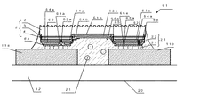
本実施形態は、図1に示すように、第1半導体層2と、活性層3と、第2半導体層4を有する半導体層5と、第2半導体層上に設けられた絶縁層62と、第2半導体層4と重なるよう前記絶縁層62上に設けられる前記第1半導体層2と電気的に接続されるn側電極6bと、前記第2半導体層4と電気的に接続されるp側電極6aと、を備える構造体7の発光素子9’のp側電極6aおよびn側電極6bと、基体12を備える支持体20のp側配線11aおよびn側配線11bとが、導電性粒子21とバインダ樹脂22を備える異方性導電材料23によって、それぞれ電気的に接続されている態様に関する。そして、基板1は半導体層5から除去されている。
まず、図2(a)〜(f)に示すように、基板と、第1半導体層と、第2半導体層と、第2半導体層上に設けられた絶縁層と、第2半導体層と重なるよう前記絶縁層上に設けられる前記第1半導体層と電気的に接続されるn側電極と、前記第2半導体層と電気的に接続されるp側電極と、を有する構造体7を準備する。
本発明の発光装置において、発光素子は複数の導電部材と複数の絶縁層(例えばそれぞれ2層以上)を有していてもよい。
異方性導電材料として、フィルム状の異方性導電材料(ACF)を用いること以外は、実施例1と同様に発光装置を製造する。本実施例では、支持体20上にフィルム状の異方性導電材料23を載置することで、ディスペンス法によらず異方性導電材料23を供給できるため、量産性を向上させることができる。また、本実施例では、液状の異方性導電材料を用いる場合と異なり、壁部23aが高く形成されないため、壁部を除去する工程を削減することができ、量産性を向上させることができる。(図15参照)
2 n型半導体層
3 活性層
4 p型半導体層
5 半導体層
5a 上面
6a p側電極(金属部材)
6b n側電極(金属部材)
61a p側導電部材(p側第1導電部材)
61b n側導電部材(n側第1導電部材)
62 絶縁層(第1絶縁層)
63a 貫通孔(第1貫通孔)
63b 貫通孔(第1貫通孔)
64a p側第2導電部材
64b n側第2導電部材
65 第2絶縁層
66a 第2貫通孔
66b 第2貫通孔
7構造体
8a、8b バンプ
9、10、91、92 チップ
9’、10’、91’、92’ 発光素子
11a p側配線
11b n側配線
12 基材
13a、13b リード
14a、14b ビア
20 支持体
200 集合基板
21 導電性粒子
21a コア(第2樹脂)
21b 導電性層
22 バインダ樹脂(第1樹脂)
23 異方性導電材料
23a 壁部
24、24’ヒートツール
32、32’蛍光体層
33 封止樹脂(第3樹脂)
41、42 発光装置
Claims (13)
- 発光素子が支持体にフリップチップ実装された発光装置の製造方法であって、
(a)基板と、前記基板上に形成された第1半導体層と第2半導体層と、を含む半導体層と、前記第1半導体層と電気的に接続されるn側電極と、前記第2半導体層と電気的に接続されるp側電極と、前記基板と反対側の面において、前記第1半導体層と前記第2半導体層に重なるよう設けられた金属部材を有する構造体を準備し、
(b)p側配線およびn側配線を同一面上に有する支持体を準備し、
(c)前記構造体のp側電極およびn側電極と前記支持体のp側配線およびn側配線とを、導電性粒子および第1樹脂を含む異方性導電材料を用いて、それぞれ電気的に接続し、その後、
(d)前記基板を前記構造体から除去して発光素子とすることを含む、発光装置の製造方法。 - 前記金属部材は、絶縁層を挟んで前記第2半導体層と重なるように設けられる請求項1に記載の発光装置の製造方法。
- 前記金属部材が、前記第2半導体層と重なるよう設けられた前記n側電極である請求項1または2に記載の発光装置の製造方法。
- 前記接着部材は、前記構造体と前記支持体との間にほぼ完全に充填されている請求項1ないし3のいずれか1項に記載の発光装置の製造方法。
- 前記基板を分離する工程は、前記基板を透過する波長のレーザー照射によって行われる請求項1ないし4のいずれか1項記載の発光装置の製造方法。
- 前記第n側電極と前記p側電極との高さの差が、前記第1半導体層と前記第2半導体層との高さの差よりも小さくなるよう設けられる請求項1から5のいずれか1項に記載の発光装置の製造方法。
- 前記支持体は、前記支持体が複数連結した集合基板として準備される請求項1から6のいずれか1項に記載の発光装置の製造方法。
- 前記集合基板を分割して発光装置を得る工程を含む請求項7に記載の発光装置の製造方法。
- 第1半導体層と、第2半導体層と、を含む半導体層と、前記第1半導体層と電気的に接続されるn側電極と、前記第2半導体層と接続されるp側電極とを有し、最上面が前記半導体層である発光素子と、p側配線およびn側配線を同一面上に有する支持体と、を備え、前記発光素子のp側電極およびn側電極と前記支持体のp側配線およびn側配線とが、異方性導電材料によって、それぞれ電気的に接続されており、前記発光素子は、前記第1半導体層の反対側の面において、前記第1半導体層と前記第2半導体層に重なるよう設けられた金属部材を備えることを特徴とする発光装置。
- 前記金属部材は、絶縁層を挟んで前記第2半導体層と重なるように設けられる請求項9に記載の発光装置。
- 前記金属部材が、前記第2半導体層と重なるよう設けられた前記n側電極である請求項9または10に記載の発光装置。
- 前記異方性導電材料は、前記発光素子と前記支持体との間にほぼ完全に充填されている請求項9からに記載の発光装置。
- 前記第n側電極と前記p側電極との高さの差が、前記第1半導体層と前記第2半導体層との高さの差よりも小さい請求項8から10のいずれか1項に記載の発光装置。
Priority Applications (4)
| Application Number | Priority Date | Filing Date | Title |
|---|---|---|---|
| JP2013054267A JP2014179569A (ja) | 2013-03-15 | 2013-03-15 | 発光装置およびその製造方法 |
| US14/011,628 US9337405B2 (en) | 2012-08-31 | 2013-08-27 | Light emitting device and method for manufacturing the same |
| CN201310381486.3A CN103682038B (zh) | 2012-08-31 | 2013-08-28 | 发光装置及其制造方法 |
| EP13182215.7A EP2704223B1 (en) | 2012-08-31 | 2013-08-29 | Light emitting device and method for manufacturing the same |
Applications Claiming Priority (1)
| Application Number | Priority Date | Filing Date | Title |
|---|---|---|---|
| JP2013054267A JP2014179569A (ja) | 2013-03-15 | 2013-03-15 | 発光装置およびその製造方法 |
Publications (2)
| Publication Number | Publication Date |
|---|---|
| JP2014179569A true JP2014179569A (ja) | 2014-09-25 |
| JP2014179569A5 JP2014179569A5 (ja) | 2016-02-12 |
Family
ID=51699197
Family Applications (1)
| Application Number | Title | Priority Date | Filing Date |
|---|---|---|---|
| JP2013054267A Pending JP2014179569A (ja) | 2012-08-31 | 2013-03-15 | 発光装置およびその製造方法 |
Country Status (1)
| Country | Link |
|---|---|
| JP (1) | JP2014179569A (ja) |
Cited By (7)
| Publication number | Priority date | Publication date | Assignee | Title |
|---|---|---|---|---|
| JP2016127056A (ja) * | 2014-12-26 | 2016-07-11 | 日亜化学工業株式会社 | 発光装置 |
| JP2017045832A (ja) * | 2015-08-26 | 2017-03-02 | 日亜化学工業株式会社 | 発光装置及び発光装置の製造方法 |
| JP2017534122A (ja) * | 2014-11-14 | 2017-11-16 | 深▲セン▼市華星光電技術有限公司 | 相互キャパシタンス方式のogsタッチパネル及びその製造方法 |
| JP2019029546A (ja) * | 2017-07-31 | 2019-02-21 | 日亜化学工業株式会社 | 半導体発光装置の製造方法 |
| JP2019176192A (ja) * | 2014-12-26 | 2019-10-10 | 日亜化学工業株式会社 | 発光装置 |
| KR20200031978A (ko) * | 2018-09-14 | 2020-03-25 | 칩본드 테크놀러지 코포레이션 | 칩 패키지 구조 및 그 칩 |
| JP2021170526A (ja) * | 2020-04-13 | 2021-10-28 | 日亜化学工業株式会社 | 面状光源及びその製造方法 |
Citations (7)
| Publication number | Priority date | Publication date | Assignee | Title |
|---|---|---|---|---|
| JP2000114595A (ja) * | 1998-10-07 | 2000-04-21 | Matsushita Electronics Industry Corp | GaN系化合物半導体発光素子 |
| JP2003017757A (ja) * | 2001-06-29 | 2003-01-17 | Sanken Electric Co Ltd | フリップチップ形半導体発光素子 |
| JP2006344971A (ja) * | 2005-06-09 | 2006-12-21 | Philips Lumileds Lightng Co Llc | 半導体発光素子の成長基板を除去する方法 |
| JP2010533374A (ja) * | 2007-07-09 | 2010-10-21 | コーニンクレッカ フィリップス エレクトロニクス エヌ ヴィ | Ledの形成における基板の取り除き |
| JP2011514688A (ja) * | 2008-03-17 | 2011-05-06 | コーニンクレッカ フィリップス エレクトロニクス エヌ ヴィ | フリップチップledに関するアンダーフィル処理 |
| US20110315956A1 (en) * | 2010-06-29 | 2011-12-29 | Michael Tischler | Electronic Devices with Yielding Substrates |
| CN102354721A (zh) * | 2011-11-04 | 2012-02-15 | 祝进田 | 一种倒装结构的led芯片制作方法 |
-
2013
- 2013-03-15 JP JP2013054267A patent/JP2014179569A/ja active Pending
Patent Citations (8)
| Publication number | Priority date | Publication date | Assignee | Title |
|---|---|---|---|---|
| JP2000114595A (ja) * | 1998-10-07 | 2000-04-21 | Matsushita Electronics Industry Corp | GaN系化合物半導体発光素子 |
| JP2003017757A (ja) * | 2001-06-29 | 2003-01-17 | Sanken Electric Co Ltd | フリップチップ形半導体発光素子 |
| JP2006344971A (ja) * | 2005-06-09 | 2006-12-21 | Philips Lumileds Lightng Co Llc | 半導体発光素子の成長基板を除去する方法 |
| JP2010533374A (ja) * | 2007-07-09 | 2010-10-21 | コーニンクレッカ フィリップス エレクトロニクス エヌ ヴィ | Ledの形成における基板の取り除き |
| JP2011514688A (ja) * | 2008-03-17 | 2011-05-06 | コーニンクレッカ フィリップス エレクトロニクス エヌ ヴィ | フリップチップledに関するアンダーフィル処理 |
| US20110315956A1 (en) * | 2010-06-29 | 2011-12-29 | Michael Tischler | Electronic Devices with Yielding Substrates |
| JP2013531378A (ja) * | 2010-06-29 | 2013-08-01 | クーレッジ ライティング インコーポレイテッド | 柔軟な基板を有する電子素子 |
| CN102354721A (zh) * | 2011-11-04 | 2012-02-15 | 祝进田 | 一种倒装结构的led芯片制作方法 |
Cited By (10)
| Publication number | Priority date | Publication date | Assignee | Title |
|---|---|---|---|---|
| JP2017534122A (ja) * | 2014-11-14 | 2017-11-16 | 深▲セン▼市華星光電技術有限公司 | 相互キャパシタンス方式のogsタッチパネル及びその製造方法 |
| JP2016127056A (ja) * | 2014-12-26 | 2016-07-11 | 日亜化学工業株式会社 | 発光装置 |
| JP2019176192A (ja) * | 2014-12-26 | 2019-10-10 | 日亜化学工業株式会社 | 発光装置 |
| JP2017045832A (ja) * | 2015-08-26 | 2017-03-02 | 日亜化学工業株式会社 | 発光装置及び発光装置の製造方法 |
| JP2019029546A (ja) * | 2017-07-31 | 2019-02-21 | 日亜化学工業株式会社 | 半導体発光装置の製造方法 |
| KR20200031978A (ko) * | 2018-09-14 | 2020-03-25 | 칩본드 테크놀러지 코포레이션 | 칩 패키지 구조 및 그 칩 |
| US10797213B2 (en) | 2018-09-14 | 2020-10-06 | Chipbond Technology Corporation | Chip package and chip thereof |
| KR102223668B1 (ko) * | 2018-09-14 | 2021-03-05 | 칩본드 테크놀러지 코포레이션 | 칩 패키지 구조 및 그 칩 |
| JP2021170526A (ja) * | 2020-04-13 | 2021-10-28 | 日亜化学工業株式会社 | 面状光源及びその製造方法 |
| JP7140999B2 (ja) | 2020-04-13 | 2022-09-22 | 日亜化学工業株式会社 | 面状光源及びその製造方法 |
Similar Documents
| Publication | Publication Date | Title |
|---|---|---|
| EP2704223B1 (en) | Light emitting device and method for manufacturing the same | |
| US11056627B2 (en) | Light emitting device | |
| JP6687073B2 (ja) | 発光装置 | |
| JP6323176B2 (ja) | 発光装置の製造方法 | |
| JP6205897B2 (ja) | 発光装置及びその製造方法 | |
| JP2014179569A (ja) | 発光装置およびその製造方法 | |
| JP6398626B2 (ja) | 発光装置の製造方法 | |
| JP6699634B2 (ja) | 発光装置の製造方法 | |
| US9136447B2 (en) | Light emitting device and method of manufacturing the same | |
| WO2013137356A1 (ja) | 半導体発光装置及びその製造方法 | |
| JP6256026B2 (ja) | 発光装置及び発光装置の製造方法 | |
| US20160064621A1 (en) | Method of manufacturing light emitting device | |
| JP6447018B2 (ja) | 発光装置及び発光装置の製造方法 | |
| JP6511809B2 (ja) | 発光装置及びその実装方法、並びに光源装置の製造方法 | |
| JP6155827B2 (ja) | 発光装置の製造方法 | |
| JP6460189B2 (ja) | 発光装置及びその製造方法 | |
| JP6089507B2 (ja) | 発光装置およびその製造方法 | |
| JP2019054277A (ja) | 発光装置及び発光装置の製造方法 | |
| JP2019067880A (ja) | 発光装置の製造方法及び発光装置 | |
| JP2020123746A (ja) | 発光装置の製造方法 |
Legal Events
| Date | Code | Title | Description |
|---|---|---|---|
| RD03 | Notification of appointment of power of attorney |
Free format text: JAPANESE INTERMEDIATE CODE: A7423 Effective date: 20150908 |
|
| A521 | Request for written amendment filed |
Free format text: JAPANESE INTERMEDIATE CODE: A523 Effective date: 20151221 |
|
| A621 | Written request for application examination |
Free format text: JAPANESE INTERMEDIATE CODE: A621 Effective date: 20151221 |
|
| RD04 | Notification of resignation of power of attorney |
Free format text: JAPANESE INTERMEDIATE CODE: A7424 Effective date: 20160215 |
|
| A977 | Report on retrieval |
Free format text: JAPANESE INTERMEDIATE CODE: A971007 Effective date: 20160729 |
|
| A131 | Notification of reasons for refusal |
Free format text: JAPANESE INTERMEDIATE CODE: A131 Effective date: 20160802 |
|
| A601 | Written request for extension of time |
Free format text: JAPANESE INTERMEDIATE CODE: A601 Effective date: 20160926 |
|
| A521 | Request for written amendment filed |
Free format text: JAPANESE INTERMEDIATE CODE: A523 Effective date: 20161125 |
|
| A131 | Notification of reasons for refusal |
Free format text: JAPANESE INTERMEDIATE CODE: A131 Effective date: 20170411 |
|
| A02 | Decision of refusal |
Free format text: JAPANESE INTERMEDIATE CODE: A02 Effective date: 20171010 |