JP2014017354A - 成膜方法 - Google Patents
成膜方法 Download PDFInfo
- Publication number
- JP2014017354A JP2014017354A JP2012153407A JP2012153407A JP2014017354A JP 2014017354 A JP2014017354 A JP 2014017354A JP 2012153407 A JP2012153407 A JP 2012153407A JP 2012153407 A JP2012153407 A JP 2012153407A JP 2014017354 A JP2014017354 A JP 2014017354A
- Authority
- JP
- Japan
- Prior art keywords
- gas
- film
- wafer
- film forming
- substrate
- Prior art date
- Legal status (The legal status is an assumption and is not a legal conclusion. Google has not performed a legal analysis and makes no representation as to the accuracy of the status listed.)
- Pending
Links
Images


Classifications
-
- H—ELECTRICITY
- H01—ELECTRIC ELEMENTS
- H01L—SEMICONDUCTOR DEVICES NOT COVERED BY CLASS H10
- H01L21/00—Processes or apparatus adapted for the manufacture or treatment of semiconductor or solid state devices or of parts thereof
- H01L21/02—Manufacture or treatment of semiconductor devices or of parts thereof
- H01L21/04—Manufacture or treatment of semiconductor devices or of parts thereof the devices having at least one potential-jump barrier or surface barrier, e.g. PN junction, depletion layer or carrier concentration layer
- H01L21/18—Manufacture or treatment of semiconductor devices or of parts thereof the devices having at least one potential-jump barrier or surface barrier, e.g. PN junction, depletion layer or carrier concentration layer the devices having semiconductor bodies comprising elements of Group IV of the Periodic System or AIIIBV compounds with or without impurities, e.g. doping materials
- H01L21/28—Manufacture of electrodes on semiconductor bodies using processes or apparatus not provided for in groups H01L21/20 - H01L21/268
- H01L21/283—Deposition of conductive or insulating materials for electrodes conducting electric current
- H01L21/285—Deposition of conductive or insulating materials for electrodes conducting electric current from a gas or vapour, e.g. condensation
- H01L21/28506—Deposition of conductive or insulating materials for electrodes conducting electric current from a gas or vapour, e.g. condensation of conductive layers
- H01L21/28512—Deposition of conductive or insulating materials for electrodes conducting electric current from a gas or vapour, e.g. condensation of conductive layers on semiconductor bodies comprising elements of Group IV of the Periodic System
- H01L21/28556—Deposition of conductive or insulating materials for electrodes conducting electric current from a gas or vapour, e.g. condensation of conductive layers on semiconductor bodies comprising elements of Group IV of the Periodic System by chemical means, e.g. CVD, LPCVD, PECVD, laser CVD
-
- H—ELECTRICITY
- H01—ELECTRIC ELEMENTS
- H01L—SEMICONDUCTOR DEVICES NOT COVERED BY CLASS H10
- H01L21/00—Processes or apparatus adapted for the manufacture or treatment of semiconductor or solid state devices or of parts thereof
- H01L21/70—Manufacture or treatment of devices consisting of a plurality of solid state components formed in or on a common substrate or of parts thereof; Manufacture of integrated circuit devices or of parts thereof
- H01L21/71—Manufacture of specific parts of devices defined in group H01L21/70
- H01L21/76—Making of isolation regions between components
-
- C—CHEMISTRY; METALLURGY
- C23—COATING METALLIC MATERIAL; COATING MATERIAL WITH METALLIC MATERIAL; CHEMICAL SURFACE TREATMENT; DIFFUSION TREATMENT OF METALLIC MATERIAL; COATING BY VACUUM EVAPORATION, BY SPUTTERING, BY ION IMPLANTATION OR BY CHEMICAL VAPOUR DEPOSITION, IN GENERAL; INHIBITING CORROSION OF METALLIC MATERIAL OR INCRUSTATION IN GENERAL
- C23C—COATING METALLIC MATERIAL; COATING MATERIAL WITH METALLIC MATERIAL; SURFACE TREATMENT OF METALLIC MATERIAL BY DIFFUSION INTO THE SURFACE, BY CHEMICAL CONVERSION OR SUBSTITUTION; COATING BY VACUUM EVAPORATION, BY SPUTTERING, BY ION IMPLANTATION OR BY CHEMICAL VAPOUR DEPOSITION, IN GENERAL
- C23C16/00—Chemical coating by decomposition of gaseous compounds, without leaving reaction products of surface material in the coating, i.e. chemical vapour deposition [CVD] processes
- C23C16/22—Chemical coating by decomposition of gaseous compounds, without leaving reaction products of surface material in the coating, i.e. chemical vapour deposition [CVD] processes characterised by the deposition of inorganic material, other than metallic material
- C23C16/30—Deposition of compounds, mixtures or solid solutions, e.g. borides, carbides, nitrides
- C23C16/40—Oxides
-
- C—CHEMISTRY; METALLURGY
- C23—COATING METALLIC MATERIAL; COATING MATERIAL WITH METALLIC MATERIAL; CHEMICAL SURFACE TREATMENT; DIFFUSION TREATMENT OF METALLIC MATERIAL; COATING BY VACUUM EVAPORATION, BY SPUTTERING, BY ION IMPLANTATION OR BY CHEMICAL VAPOUR DEPOSITION, IN GENERAL; INHIBITING CORROSION OF METALLIC MATERIAL OR INCRUSTATION IN GENERAL
- C23C—COATING METALLIC MATERIAL; COATING MATERIAL WITH METALLIC MATERIAL; SURFACE TREATMENT OF METALLIC MATERIAL BY DIFFUSION INTO THE SURFACE, BY CHEMICAL CONVERSION OR SUBSTITUTION; COATING BY VACUUM EVAPORATION, BY SPUTTERING, BY ION IMPLANTATION OR BY CHEMICAL VAPOUR DEPOSITION, IN GENERAL
- C23C16/00—Chemical coating by decomposition of gaseous compounds, without leaving reaction products of surface material in the coating, i.e. chemical vapour deposition [CVD] processes
- C23C16/44—Chemical coating by decomposition of gaseous compounds, without leaving reaction products of surface material in the coating, i.e. chemical vapour deposition [CVD] processes characterised by the method of coating
- C23C16/455—Chemical coating by decomposition of gaseous compounds, without leaving reaction products of surface material in the coating, i.e. chemical vapour deposition [CVD] processes characterised by the method of coating characterised by the method used for introducing gases into reaction chamber or for modifying gas flows in reaction chamber
- C23C16/45523—Pulsed gas flow or change of composition over time
- C23C16/45525—Atomic layer deposition [ALD]
- C23C16/45527—Atomic layer deposition [ALD] characterized by the ALD cycle, e.g. different flows or temperatures during half-reactions, unusual pulsing sequence, use of precursor mixtures or auxiliary reactants or activations
- C23C16/45531—Atomic layer deposition [ALD] characterized by the ALD cycle, e.g. different flows or temperatures during half-reactions, unusual pulsing sequence, use of precursor mixtures or auxiliary reactants or activations specially adapted for making ternary or higher compositions
-
- H—ELECTRICITY
- H01—ELECTRIC ELEMENTS
- H01L—SEMICONDUCTOR DEVICES NOT COVERED BY CLASS H10
- H01L21/00—Processes or apparatus adapted for the manufacture or treatment of semiconductor or solid state devices or of parts thereof
- H01L21/02—Manufacture or treatment of semiconductor devices or of parts thereof
- H01L21/02104—Forming layers
- H01L21/02107—Forming insulating materials on a substrate
- H01L21/02109—Forming insulating materials on a substrate characterised by the type of layer, e.g. type of material, porous/non-porous, pre-cursors, mixtures or laminates
- H01L21/02112—Forming insulating materials on a substrate characterised by the type of layer, e.g. type of material, porous/non-porous, pre-cursors, mixtures or laminates characterised by the material of the layer
- H01L21/02172—Forming insulating materials on a substrate characterised by the type of layer, e.g. type of material, porous/non-porous, pre-cursors, mixtures or laminates characterised by the material of the layer the material containing at least one metal element, e.g. metal oxides, metal nitrides, metal oxynitrides or metal carbides
- H01L21/02175—Forming insulating materials on a substrate characterised by the type of layer, e.g. type of material, porous/non-porous, pre-cursors, mixtures or laminates characterised by the material of the layer the material containing at least one metal element, e.g. metal oxides, metal nitrides, metal oxynitrides or metal carbides characterised by the metal
- H01L21/02178—Forming insulating materials on a substrate characterised by the type of layer, e.g. type of material, porous/non-porous, pre-cursors, mixtures or laminates characterised by the material of the layer the material containing at least one metal element, e.g. metal oxides, metal nitrides, metal oxynitrides or metal carbides characterised by the metal the material containing aluminium, e.g. Al2O3
-
- H—ELECTRICITY
- H01—ELECTRIC ELEMENTS
- H01L—SEMICONDUCTOR DEVICES NOT COVERED BY CLASS H10
- H01L21/00—Processes or apparatus adapted for the manufacture or treatment of semiconductor or solid state devices or of parts thereof
- H01L21/02—Manufacture or treatment of semiconductor devices or of parts thereof
- H01L21/02104—Forming layers
- H01L21/02107—Forming insulating materials on a substrate
- H01L21/02109—Forming insulating materials on a substrate characterised by the type of layer, e.g. type of material, porous/non-porous, pre-cursors, mixtures or laminates
- H01L21/02112—Forming insulating materials on a substrate characterised by the type of layer, e.g. type of material, porous/non-porous, pre-cursors, mixtures or laminates characterised by the material of the layer
- H01L21/02172—Forming insulating materials on a substrate characterised by the type of layer, e.g. type of material, porous/non-porous, pre-cursors, mixtures or laminates characterised by the material of the layer the material containing at least one metal element, e.g. metal oxides, metal nitrides, metal oxynitrides or metal carbides
- H01L21/02175—Forming insulating materials on a substrate characterised by the type of layer, e.g. type of material, porous/non-porous, pre-cursors, mixtures or laminates characterised by the material of the layer the material containing at least one metal element, e.g. metal oxides, metal nitrides, metal oxynitrides or metal carbides characterised by the metal
- H01L21/02189—Forming insulating materials on a substrate characterised by the type of layer, e.g. type of material, porous/non-porous, pre-cursors, mixtures or laminates characterised by the material of the layer the material containing at least one metal element, e.g. metal oxides, metal nitrides, metal oxynitrides or metal carbides characterised by the metal the material containing zirconium, e.g. ZrO2
-
- H—ELECTRICITY
- H01—ELECTRIC ELEMENTS
- H01L—SEMICONDUCTOR DEVICES NOT COVERED BY CLASS H10
- H01L21/00—Processes or apparatus adapted for the manufacture or treatment of semiconductor or solid state devices or of parts thereof
- H01L21/02—Manufacture or treatment of semiconductor devices or of parts thereof
- H01L21/02104—Forming layers
- H01L21/02107—Forming insulating materials on a substrate
- H01L21/02109—Forming insulating materials on a substrate characterised by the type of layer, e.g. type of material, porous/non-porous, pre-cursors, mixtures or laminates
- H01L21/02112—Forming insulating materials on a substrate characterised by the type of layer, e.g. type of material, porous/non-porous, pre-cursors, mixtures or laminates characterised by the material of the layer
- H01L21/02172—Forming insulating materials on a substrate characterised by the type of layer, e.g. type of material, porous/non-porous, pre-cursors, mixtures or laminates characterised by the material of the layer the material containing at least one metal element, e.g. metal oxides, metal nitrides, metal oxynitrides or metal carbides
- H01L21/02175—Forming insulating materials on a substrate characterised by the type of layer, e.g. type of material, porous/non-porous, pre-cursors, mixtures or laminates characterised by the material of the layer the material containing at least one metal element, e.g. metal oxides, metal nitrides, metal oxynitrides or metal carbides characterised by the metal
- H01L21/02194—Forming insulating materials on a substrate characterised by the type of layer, e.g. type of material, porous/non-porous, pre-cursors, mixtures or laminates characterised by the material of the layer the material containing at least one metal element, e.g. metal oxides, metal nitrides, metal oxynitrides or metal carbides characterised by the metal the material containing more than one metal element
-
- H—ELECTRICITY
- H01—ELECTRIC ELEMENTS
- H01L—SEMICONDUCTOR DEVICES NOT COVERED BY CLASS H10
- H01L21/00—Processes or apparatus adapted for the manufacture or treatment of semiconductor or solid state devices or of parts thereof
- H01L21/02—Manufacture or treatment of semiconductor devices or of parts thereof
- H01L21/02104—Forming layers
- H01L21/02107—Forming insulating materials on a substrate
- H01L21/02225—Forming insulating materials on a substrate characterised by the process for the formation of the insulating layer
- H01L21/0226—Forming insulating materials on a substrate characterised by the process for the formation of the insulating layer formation by a deposition process
- H01L21/02263—Forming insulating materials on a substrate characterised by the process for the formation of the insulating layer formation by a deposition process deposition from the gas or vapour phase
- H01L21/02271—Forming insulating materials on a substrate characterised by the process for the formation of the insulating layer formation by a deposition process deposition from the gas or vapour phase deposition by decomposition or reaction of gaseous or vapour phase compounds, i.e. chemical vapour deposition
- H01L21/02274—Forming insulating materials on a substrate characterised by the process for the formation of the insulating layer formation by a deposition process deposition from the gas or vapour phase deposition by decomposition or reaction of gaseous or vapour phase compounds, i.e. chemical vapour deposition in the presence of a plasma [PECVD]
-
- H—ELECTRICITY
- H01—ELECTRIC ELEMENTS
- H01L—SEMICONDUCTOR DEVICES NOT COVERED BY CLASS H10
- H01L21/00—Processes or apparatus adapted for the manufacture or treatment of semiconductor or solid state devices or of parts thereof
- H01L21/02—Manufacture or treatment of semiconductor devices or of parts thereof
- H01L21/02104—Forming layers
- H01L21/02107—Forming insulating materials on a substrate
- H01L21/02225—Forming insulating materials on a substrate characterised by the process for the formation of the insulating layer
- H01L21/0226—Forming insulating materials on a substrate characterised by the process for the formation of the insulating layer formation by a deposition process
- H01L21/02263—Forming insulating materials on a substrate characterised by the process for the formation of the insulating layer formation by a deposition process deposition from the gas or vapour phase
- H01L21/02271—Forming insulating materials on a substrate characterised by the process for the formation of the insulating layer formation by a deposition process deposition from the gas or vapour phase deposition by decomposition or reaction of gaseous or vapour phase compounds, i.e. chemical vapour deposition
- H01L21/0228—Forming insulating materials on a substrate characterised by the process for the formation of the insulating layer formation by a deposition process deposition from the gas or vapour phase deposition by decomposition or reaction of gaseous or vapour phase compounds, i.e. chemical vapour deposition deposition by cyclic CVD, e.g. ALD, ALE, pulsed CVD
-
- H—ELECTRICITY
- H01—ELECTRIC ELEMENTS
- H01L—SEMICONDUCTOR DEVICES NOT COVERED BY CLASS H10
- H01L21/00—Processes or apparatus adapted for the manufacture or treatment of semiconductor or solid state devices or of parts thereof
- H01L21/67—Apparatus specially adapted for handling semiconductor or electric solid state devices during manufacture or treatment thereof; Apparatus specially adapted for handling wafers during manufacture or treatment of semiconductor or electric solid state devices or components ; Apparatus not specifically provided for elsewhere
- H01L21/677—Apparatus specially adapted for handling semiconductor or electric solid state devices during manufacture or treatment thereof; Apparatus specially adapted for handling wafers during manufacture or treatment of semiconductor or electric solid state devices or components ; Apparatus not specifically provided for elsewhere for conveying, e.g. between different workstations
- H01L21/67739—Apparatus specially adapted for handling semiconductor or electric solid state devices during manufacture or treatment thereof; Apparatus specially adapted for handling wafers during manufacture or treatment of semiconductor or electric solid state devices or components ; Apparatus not specifically provided for elsewhere for conveying, e.g. between different workstations into and out of processing chamber
- H01L21/67748—Apparatus specially adapted for handling semiconductor or electric solid state devices during manufacture or treatment thereof; Apparatus specially adapted for handling wafers during manufacture or treatment of semiconductor or electric solid state devices or components ; Apparatus not specifically provided for elsewhere for conveying, e.g. between different workstations into and out of processing chamber horizontal transfer of a single workpiece
-
- H—ELECTRICITY
- H01—ELECTRIC ELEMENTS
- H01L—SEMICONDUCTOR DEVICES NOT COVERED BY CLASS H10
- H01L21/00—Processes or apparatus adapted for the manufacture or treatment of semiconductor or solid state devices or of parts thereof
- H01L21/67—Apparatus specially adapted for handling semiconductor or electric solid state devices during manufacture or treatment thereof; Apparatus specially adapted for handling wafers during manufacture or treatment of semiconductor or electric solid state devices or components ; Apparatus not specifically provided for elsewhere
- H01L21/683—Apparatus specially adapted for handling semiconductor or electric solid state devices during manufacture or treatment thereof; Apparatus specially adapted for handling wafers during manufacture or treatment of semiconductor or electric solid state devices or components ; Apparatus not specifically provided for elsewhere for supporting or gripping
- H01L21/687—Apparatus specially adapted for handling semiconductor or electric solid state devices during manufacture or treatment thereof; Apparatus specially adapted for handling wafers during manufacture or treatment of semiconductor or electric solid state devices or components ; Apparatus not specifically provided for elsewhere for supporting or gripping using mechanical means, e.g. chucks, clamps or pinches
- H01L21/68714—Apparatus specially adapted for handling semiconductor or electric solid state devices during manufacture or treatment thereof; Apparatus specially adapted for handling wafers during manufacture or treatment of semiconductor or electric solid state devices or components ; Apparatus not specifically provided for elsewhere for supporting or gripping using mechanical means, e.g. chucks, clamps or pinches the wafers being placed on a susceptor, stage or support
- H01L21/68764—Apparatus specially adapted for handling semiconductor or electric solid state devices during manufacture or treatment thereof; Apparatus specially adapted for handling wafers during manufacture or treatment of semiconductor or electric solid state devices or components ; Apparatus not specifically provided for elsewhere for supporting or gripping using mechanical means, e.g. chucks, clamps or pinches the wafers being placed on a susceptor, stage or support characterised by a movable susceptor, stage or support, others than those only rotating on their own vertical axis, e.g. susceptors on a rotating caroussel
-
- H—ELECTRICITY
- H01—ELECTRIC ELEMENTS
- H01L—SEMICONDUCTOR DEVICES NOT COVERED BY CLASS H10
- H01L21/00—Processes or apparatus adapted for the manufacture or treatment of semiconductor or solid state devices or of parts thereof
- H01L21/67—Apparatus specially adapted for handling semiconductor or electric solid state devices during manufacture or treatment thereof; Apparatus specially adapted for handling wafers during manufacture or treatment of semiconductor or electric solid state devices or components ; Apparatus not specifically provided for elsewhere
- H01L21/683—Apparatus specially adapted for handling semiconductor or electric solid state devices during manufacture or treatment thereof; Apparatus specially adapted for handling wafers during manufacture or treatment of semiconductor or electric solid state devices or components ; Apparatus not specifically provided for elsewhere for supporting or gripping
- H01L21/687—Apparatus specially adapted for handling semiconductor or electric solid state devices during manufacture or treatment thereof; Apparatus specially adapted for handling wafers during manufacture or treatment of semiconductor or electric solid state devices or components ; Apparatus not specifically provided for elsewhere for supporting or gripping using mechanical means, e.g. chucks, clamps or pinches
- H01L21/68714—Apparatus specially adapted for handling semiconductor or electric solid state devices during manufacture or treatment thereof; Apparatus specially adapted for handling wafers during manufacture or treatment of semiconductor or electric solid state devices or components ; Apparatus not specifically provided for elsewhere for supporting or gripping using mechanical means, e.g. chucks, clamps or pinches the wafers being placed on a susceptor, stage or support
- H01L21/68771—Apparatus specially adapted for handling semiconductor or electric solid state devices during manufacture or treatment thereof; Apparatus specially adapted for handling wafers during manufacture or treatment of semiconductor or electric solid state devices or components ; Apparatus not specifically provided for elsewhere for supporting or gripping using mechanical means, e.g. chucks, clamps or pinches the wafers being placed on a susceptor, stage or support characterised by supporting more than one semiconductor substrate
Abstract
【解決手段】第1の金属を含有する第1の原料ガスに基板を晒し、当該基板を、前記第1の原料ガスと反応する反応ガスに晒すサイクルを1回以上行って第1の金属化合物の膜を前記基板に成膜する第1の成膜ステップと、前記第1の金属化合物の膜が成膜された前記基板を、前記第1の原料ガスに晒し、前記第1の金属化合物の膜に前記第1の金属を吸着させる吸着ステップと、前記第1の金属が吸着された前記基板を、第2の金属を含有する第2の原料ガスに晒し、当該基板を、前記第2の原料ガスと反応する反応ガスに晒すサイクルを1回以上行って第2の金属化合物の膜を前記基板に成膜する第2の成膜ステップとを含む成膜方法により上記の課題が達成される。
【選択図】図3
Description
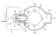
以下、図1及び図2を参照しながら、本発明の実施形態による成膜方法を実施するに好適な成膜装置を説明する。
図1及び図2を参照すると、成膜装置2は、下端が開口された有天井の円筒体状の処理容器4を有している。この処理容器4の全体は、例えば石英により形成されており、この処理容器4内の天井には、石英製の天井板6が設けられて封止されている。また、この処理容器4の下端開口部には、フランジ部8が設けられている。なお、処理容器4の下端にステンレススチール製のマニホールドを設けてもよい。
なお、図示の便宜上、各ノズル38、40、42、及び44は処理容器4の下部側壁を貫通しているが、実際にはフランジ部8から挿入されている。
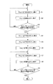
次に、図1から図3までを参照しながら、本発明の実施形態による成膜方法を上述の成膜装置2において実施する場合を例にとり説明する。まず、例えば50〜100枚の直径300mmを有するウエハWが搭載されたウエハボート12(図1)を予め所定の温度に設定された処理容器4内に下方より搬入し、蓋部18で処理容器4の下端開口部を閉じる。次いで、パージガス供給部34から処理容器4内へN2ガスを供給すると共に、圧力調整弁86及び真空ポンプ88により、処理容器4内を所定のプロセス圧力に維持する。また、加熱部92への供給電力を増大させてウエハWを所定のプロセス温度に維持する。
所定の時間が経過した後、ガス供給部30の開閉バルブ50Aを閉じることによりTEMAZガスの処理容器4への供給を停止すると、パージガス供給部34からのN2により処理容器4内がパージされる。
ステップS1とS2のサイクルが所定の回数行われていない場合(ステップS3:NO)、ステップS1に戻り、ステップS1とS2が繰り返される。一方、このサイクルが所定の回数行われ、所定の膜厚を有するZrO膜(以下、第1のZrO膜という)が成膜された場合には(ステップS3:YES)、ステップS4へ進む。すなわち、ガス供給部30の開閉バルブ50Aを開くことにより処理容器4にTEMAZガスを供給し、ウエハボート12に搭載されるウエハWをTEMAZガスに晒す。これにより、所定の厚さで成膜されている第1のZrO膜上にTEMAZガスが吸着される。
次いで、所定の時間が経過した後、開閉バルブ52Aを閉じることによりTMAガスの処理容器4への供給を停止すると、パージガス供給部34からのN2により処理容器4内がパージされる。
次に、ステップS7からステップS9(図3)が行われる。これらのステップは、ステップS1からステップS3に対応しており、これらのステップを行うことにより、ZrAlO膜上に、所定の膜厚を有するZrO膜(以下、第2のZrO膜という)が成膜される。この後、処理容器4内がN2ガスでパージされた後にウエハボート12が処理容器4から搬出される。
図4は、成膜装置の概略断面であり、図5及び図6は、真空容器110内の構造を説明する図である。図5及び図6では、説明の便宜上、天板111の図示を省略している。
反応ガスノズル310には、三方弁及び流量調整器を介してTEMAZガス供給源とTMAガス供給源(いずれも不図示)とが接続され、三方弁の切り替えにより、所定の流量でTEMAZガスとTMAガスとが選択的に反応ガスノズル310を通して真空容器110へ供給される。また、反応ガスノズル320には、オゾン(O3)ガス供給源(不図示)が開閉バルブ及び流量調整器(ともに不図示)を介して接続され、反応ガスノズル320通して真空容器110へオゾンガスが供給される。なお、反応ガスノズル310の下方領域を、TEMAZガス及びTMAガスを選択的にウエハWに吸着させるための第1の処理領域P1と言い、反応ガスノズル320の下方領域を、第1の処理領域P1においてウエハWに吸着されたTEMAZガス且つ/又はTMAガスを酸化させる第2の処理領域P2と言う場合がある。
Claims (8)
- 第1の金属を含有する第1の原料ガスに基板を晒し、当該基板を、前記第1の原料ガスと反応する反応ガスに晒す第1のサイクルを行って第1の金属化合物の膜を前記基板に成膜する第1の成膜ステップと、
前記第1の金属化合物の膜が成膜された前記基板を、前記第1の原料ガスに晒し、前記第1の金属化合物の膜に前記第1の原料ガスを吸着させる吸着ステップと、
前記第1の原料ガスが吸着された前記基板を、第2の金属を含有する第2の原料ガスに晒し、当該基板を、前記第2の原料ガスと反応する反応ガスに晒す第2のサイクルを行って第2の金属化合物の膜を前記基板に成膜する第2の成膜ステップと
を含む成膜方法。 - 前記第2の成膜ステップの後に、前記第1の成膜ステップが再び行われる、請求項1に記載の成膜方法。
- 前記第1の成膜ステップ、前記吸着ステップ、及び前記第2の成膜ステップがこの順に繰り返される、請求項1又は2に記載の成膜方法。
- 前記第1の成膜ステップにおいて、前記第1のサイクルが1回以上繰り返される、請求項1から3のいずれか一項に記載の成膜方法。
- 前記第1の金属がジルコニウムであり、前記第2の金属がアルミニウムである、請求項1から4のいずれか一項に記載の成膜方法。
- 前記第1の原料ガスがジルコニウムの有機金属を含み、前記第2の原料ガスがアルミニウムの有機金属を含む、請求項1から5のいずれか一項に記載の成膜方法。
- 前記ジルコニウムの有機金属がテトラキス・エチルメチル・アミノジルコニウムであり、前記アルミニウムの有機金属がトリメチル・アルミニウムである、請求項6に記載の成膜方法。
- 前記反応ガスが酸素を含む、請求項5から7のいずれか一項に記載の成膜方法。
Priority Applications (4)
| Application Number | Priority Date | Filing Date | Title |
|---|---|---|---|
| JP2012153407A JP2014017354A (ja) | 2012-07-09 | 2012-07-09 | 成膜方法 |
| TW102124317A TW201416481A (zh) | 2012-07-09 | 2013-07-08 | 成膜方法 |
| KR1020130079644A KR20140007289A (ko) | 2012-07-09 | 2013-07-08 | 성막 방법 |
| US13/937,070 US9252043B2 (en) | 2012-07-09 | 2013-07-08 | Film deposition method |
Applications Claiming Priority (1)
| Application Number | Priority Date | Filing Date | Title |
|---|---|---|---|
| JP2012153407A JP2014017354A (ja) | 2012-07-09 | 2012-07-09 | 成膜方法 |
Publications (2)
| Publication Number | Publication Date |
|---|---|
| JP2014017354A true JP2014017354A (ja) | 2014-01-30 |
| JP2014017354A5 JP2014017354A5 (ja) | 2015-01-29 |
Family
ID=49878830
Family Applications (1)
| Application Number | Title | Priority Date | Filing Date |
|---|---|---|---|
| JP2012153407A Pending JP2014017354A (ja) | 2012-07-09 | 2012-07-09 | 成膜方法 |
Country Status (4)
| Country | Link |
|---|---|
| US (1) | US9252043B2 (ja) |
| JP (1) | JP2014017354A (ja) |
| KR (1) | KR20140007289A (ja) |
| TW (1) | TW201416481A (ja) |
Cited By (1)
| Publication number | Priority date | Publication date | Assignee | Title |
|---|---|---|---|---|
| JP2018107182A (ja) * | 2016-12-22 | 2018-07-05 | 東京エレクトロン株式会社 | 基板処理装置および基板処理方法、ならびに基板処理システム |
Families Citing this family (3)
| Publication number | Priority date | Publication date | Assignee | Title |
|---|---|---|---|---|
| JP6115244B2 (ja) * | 2013-03-28 | 2017-04-19 | 東京エレクトロン株式会社 | 成膜装置 |
| US20150255267A1 (en) * | 2014-03-09 | 2015-09-10 | Tokyo Electron Limited | Atomic Layer Deposition of Aluminum-doped High-k Films |
| US11462398B2 (en) | 2019-07-17 | 2022-10-04 | International Business Machines Corporation | Ligand selection for ternary oxide thin films |
Citations (9)
| Publication number | Priority date | Publication date | Assignee | Title |
|---|---|---|---|---|
| US20050227003A1 (en) * | 2004-04-08 | 2005-10-13 | Carlson Chris M | Methods of forming material over substrates |
| JP2006135339A (ja) * | 2004-11-08 | 2006-05-25 | Hynix Semiconductor Inc | ジルコニウム酸化膜を有する半導体素子のキャパシタ及びその製造方法 |
| JP2007150242A (ja) * | 2005-11-28 | 2007-06-14 | Hynix Semiconductor Inc | 半導体素子のキャパシタ製造方法 |
| JP2007266464A (ja) * | 2006-03-29 | 2007-10-11 | Hitachi Ltd | 半導体集積回路装置の製造方法 |
| JP2011049531A (ja) * | 2009-07-31 | 2011-03-10 | Hitachi Kokusai Electric Inc | 半導体デバイスの製造方法、半導体デバイス及び基板処理装置 |
| US20110223320A1 (en) * | 2010-03-09 | 2011-09-15 | Zhe Song | Methods Of Forming Material Over A Substrate And Methods Of Forming Capacitors |
| JP2012059834A (ja) * | 2010-09-07 | 2012-03-22 | Hitachi Kokusai Electric Inc | 半導体装置の製造方法 |
| JP2012069871A (ja) * | 2010-09-27 | 2012-04-05 | Elpida Memory Inc | 半導体装置及びその製造方法、並びに吸着サイト・ブロッキング原子層堆積法 |
| JP2012124322A (ja) * | 2010-12-08 | 2012-06-28 | Elpida Memory Inc | 半導体記憶装置の製造方法 |
Family Cites Families (2)
| Publication number | Priority date | Publication date | Assignee | Title |
|---|---|---|---|---|
| JPWO2008108128A1 (ja) | 2007-03-08 | 2010-06-10 | 日本電気株式会社 | 誘電体、誘電体を用いたキャパシタ、誘電体を用いた半導体装置、及び誘電体の製造方法 |
| JP5270476B2 (ja) | 2009-07-07 | 2013-08-21 | 株式会社日立国際電気 | 半導体装置の製造方法及び基板処理装置 |
-
2012
- 2012-07-09 JP JP2012153407A patent/JP2014017354A/ja active Pending
-
2013
- 2013-07-08 US US13/937,070 patent/US9252043B2/en not_active Expired - Fee Related
- 2013-07-08 KR KR1020130079644A patent/KR20140007289A/ko not_active Application Discontinuation
- 2013-07-08 TW TW102124317A patent/TW201416481A/zh unknown
Patent Citations (9)
| Publication number | Priority date | Publication date | Assignee | Title |
|---|---|---|---|---|
| US20050227003A1 (en) * | 2004-04-08 | 2005-10-13 | Carlson Chris M | Methods of forming material over substrates |
| JP2006135339A (ja) * | 2004-11-08 | 2006-05-25 | Hynix Semiconductor Inc | ジルコニウム酸化膜を有する半導体素子のキャパシタ及びその製造方法 |
| JP2007150242A (ja) * | 2005-11-28 | 2007-06-14 | Hynix Semiconductor Inc | 半導体素子のキャパシタ製造方法 |
| JP2007266464A (ja) * | 2006-03-29 | 2007-10-11 | Hitachi Ltd | 半導体集積回路装置の製造方法 |
| JP2011049531A (ja) * | 2009-07-31 | 2011-03-10 | Hitachi Kokusai Electric Inc | 半導体デバイスの製造方法、半導体デバイス及び基板処理装置 |
| US20110223320A1 (en) * | 2010-03-09 | 2011-09-15 | Zhe Song | Methods Of Forming Material Over A Substrate And Methods Of Forming Capacitors |
| JP2012059834A (ja) * | 2010-09-07 | 2012-03-22 | Hitachi Kokusai Electric Inc | 半導体装置の製造方法 |
| JP2012069871A (ja) * | 2010-09-27 | 2012-04-05 | Elpida Memory Inc | 半導体装置及びその製造方法、並びに吸着サイト・ブロッキング原子層堆積法 |
| JP2012124322A (ja) * | 2010-12-08 | 2012-06-28 | Elpida Memory Inc | 半導体記憶装置の製造方法 |
Cited By (1)
| Publication number | Priority date | Publication date | Assignee | Title |
|---|---|---|---|---|
| JP2018107182A (ja) * | 2016-12-22 | 2018-07-05 | 東京エレクトロン株式会社 | 基板処理装置および基板処理方法、ならびに基板処理システム |
Also Published As
| Publication number | Publication date |
|---|---|
| KR20140007289A (ko) | 2014-01-17 |
| TW201416481A (zh) | 2014-05-01 |
| US20140011353A1 (en) | 2014-01-09 |
| US9252043B2 (en) | 2016-02-02 |
Similar Documents
| Publication | Publication Date | Title |
|---|---|---|
| US9076649B2 (en) | Film forming method and apparatus | |
| US8034673B2 (en) | Film formation method and apparatus for forming silicon-containing insulating film doped with metal | |
| US8257789B2 (en) | Film formation method in vertical batch CVD apparatus | |
| JP5823922B2 (ja) | 成膜方法 | |
| TWI585857B (zh) | 半導體裝置之製造方法、基板處理方法、及電腦可讀取記錄媒體 | |
| US20100068383A1 (en) | Film deposition apparatus, film deposition method, and computer readable storage medium | |
| JP6468955B2 (ja) | シリコン含有膜の成膜方法及び成膜装置 | |
| US20100068893A1 (en) | Film deposition apparatus, film deposition method, and computer readable storage medium | |
| KR101695511B1 (ko) | 성막 방법 | |
| WO2013054652A1 (ja) | 基板処理装置、基板処理方法、半導体装置の製造方法、および記録媒体 | |
| KR101575393B1 (ko) | 성막 방법 | |
| JP2011210872A (ja) | 成膜装置、成膜方法及び記憶媒体 | |
| KR20160027928A (ko) | 기판 처리 방법 및 기판 처리 장치 | |
| KR101734779B1 (ko) | 성막 방법 | |
| US9252043B2 (en) | Film deposition method | |
| JP6096955B2 (ja) | 成膜方法 | |
| US20230420249A1 (en) | Film forming method | |
| JP2014090181A (ja) | 成膜装置、成膜方法及び記憶媒体 |
Legal Events
| Date | Code | Title | Description |
|---|---|---|---|
| A521 | Request for written amendment filed |
Free format text: JAPANESE INTERMEDIATE CODE: A523 Effective date: 20141209 |
|
| A621 | Written request for application examination |
Free format text: JAPANESE INTERMEDIATE CODE: A621 Effective date: 20141209 |
|
| A977 | Report on retrieval |
Free format text: JAPANESE INTERMEDIATE CODE: A971007 Effective date: 20151008 |
|
| A131 | Notification of reasons for refusal |
Free format text: JAPANESE INTERMEDIATE CODE: A131 Effective date: 20151020 |
|
| A521 | Request for written amendment filed |
Free format text: JAPANESE INTERMEDIATE CODE: A523 Effective date: 20151202 |
|
| A131 | Notification of reasons for refusal |
Free format text: JAPANESE INTERMEDIATE CODE: A131 Effective date: 20160112 |
|
| A02 | Decision of refusal |
Free format text: JAPANESE INTERMEDIATE CODE: A02 Effective date: 20160510 |