JP2013517618A - 近接効果補正によるウェーハ及びマスクの電子ビーム照射制御方法 - Google Patents
近接効果補正によるウェーハ及びマスクの電子ビーム照射制御方法 Download PDFInfo
- Publication number
- JP2013517618A JP2013517618A JP2012548337A JP2012548337A JP2013517618A JP 2013517618 A JP2013517618 A JP 2013517618A JP 2012548337 A JP2012548337 A JP 2012548337A JP 2012548337 A JP2012548337 A JP 2012548337A JP 2013517618 A JP2013517618 A JP 2013517618A
- Authority
- JP
- Japan
- Prior art keywords
- figures
- size
- contrast
- remaining
- correction
- Prior art date
- Legal status (The legal status is an assumption and is not a legal conclusion. Google has not performed a legal analysis and makes no representation as to the accuracy of the status listed.)
- Granted
Links
Images
Classifications
-
- G—PHYSICS
- G03—PHOTOGRAPHY; CINEMATOGRAPHY; ANALOGOUS TECHNIQUES USING WAVES OTHER THAN OPTICAL WAVES; ELECTROGRAPHY; HOLOGRAPHY
- G03F—PHOTOMECHANICAL PRODUCTION OF TEXTURED OR PATTERNED SURFACES, e.g. FOR PRINTING, FOR PROCESSING OF SEMICONDUCTOR DEVICES; MATERIALS THEREFOR; ORIGINALS THEREFOR; APPARATUS SPECIALLY ADAPTED THEREFOR
- G03F7/00—Photomechanical, e.g. photolithographic, production of textured or patterned surfaces, e.g. printing surfaces; Materials therefor, e.g. comprising photoresists; Apparatus specially adapted therefor
- G03F7/20—Exposure; Apparatus therefor
-
- H—ELECTRICITY
- H01—ELECTRIC ELEMENTS
- H01J—ELECTRIC DISCHARGE TUBES OR DISCHARGE LAMPS
- H01J37/00—Discharge tubes with provision for introducing objects or material to be exposed to the discharge, e.g. for the purpose of examination or processing thereof
- H01J37/30—Electron-beam or ion-beam tubes for localised treatment of objects
- H01J37/317—Electron-beam or ion-beam tubes for localised treatment of objects for changing properties of the objects or for applying thin layers thereon, e.g. for ion implantation
- H01J37/3174—Particle-beam lithography, e.g. electron beam lithography
-
- B—PERFORMING OPERATIONS; TRANSPORTING
- B82—NANOTECHNOLOGY
- B82Y—SPECIFIC USES OR APPLICATIONS OF NANOSTRUCTURES; MEASUREMENT OR ANALYSIS OF NANOSTRUCTURES; MANUFACTURE OR TREATMENT OF NANOSTRUCTURES
- B82Y10/00—Nanotechnology for information processing, storage or transmission, e.g. quantum computing or single electron logic
-
- B—PERFORMING OPERATIONS; TRANSPORTING
- B82—NANOTECHNOLOGY
- B82Y—SPECIFIC USES OR APPLICATIONS OF NANOSTRUCTURES; MEASUREMENT OR ANALYSIS OF NANOSTRUCTURES; MANUFACTURE OR TREATMENT OF NANOSTRUCTURES
- B82Y40/00—Manufacture or treatment of nanostructures
-
- G—PHYSICS
- G03—PHOTOGRAPHY; CINEMATOGRAPHY; ANALOGOUS TECHNIQUES USING WAVES OTHER THAN OPTICAL WAVES; ELECTROGRAPHY; HOLOGRAPHY
- G03F—PHOTOMECHANICAL PRODUCTION OF TEXTURED OR PATTERNED SURFACES, e.g. FOR PRINTING, FOR PROCESSING OF SEMICONDUCTOR DEVICES; MATERIALS THEREFOR; ORIGINALS THEREFOR; APPARATUS SPECIALLY ADAPTED THEREFOR
- G03F1/00—Originals for photomechanical production of textured or patterned surfaces, e.g., masks, photo-masks, reticles; Mask blanks or pellicles therefor; Containers specially adapted therefor; Preparation thereof
- G03F1/68—Preparation processes not covered by groups G03F1/20 - G03F1/50
- G03F1/70—Adapting basic layout or design of masks to lithographic process requirements, e.g., second iteration correction of mask patterns for imaging
-
- G—PHYSICS
- G03—PHOTOGRAPHY; CINEMATOGRAPHY; ANALOGOUS TECHNIQUES USING WAVES OTHER THAN OPTICAL WAVES; ELECTROGRAPHY; HOLOGRAPHY
- G03F—PHOTOMECHANICAL PRODUCTION OF TEXTURED OR PATTERNED SURFACES, e.g. FOR PRINTING, FOR PROCESSING OF SEMICONDUCTOR DEVICES; MATERIALS THEREFOR; ORIGINALS THEREFOR; APPARATUS SPECIALLY ADAPTED THEREFOR
- G03F1/00—Originals for photomechanical production of textured or patterned surfaces, e.g., masks, photo-masks, reticles; Mask blanks or pellicles therefor; Containers specially adapted therefor; Preparation thereof
- G03F1/68—Preparation processes not covered by groups G03F1/20 - G03F1/50
- G03F1/76—Patterning of masks by imaging
- G03F1/78—Patterning of masks by imaging by charged particle beam [CPB], e.g. electron beam patterning of masks
-
- H—ELECTRICITY
- H01—ELECTRIC ELEMENTS
- H01J—ELECTRIC DISCHARGE TUBES OR DISCHARGE LAMPS
- H01J37/00—Discharge tubes with provision for introducing objects or material to be exposed to the discharge, e.g. for the purpose of examination or processing thereof
- H01J37/30—Electron-beam or ion-beam tubes for localised treatment of objects
- H01J37/317—Electron-beam or ion-beam tubes for localised treatment of objects for changing properties of the objects or for applying thin layers thereon, e.g. for ion implantation
Landscapes
- Engineering & Computer Science (AREA)
- Chemical & Material Sciences (AREA)
- Physics & Mathematics (AREA)
- Nanotechnology (AREA)
- General Physics & Mathematics (AREA)
- Crystallography & Structural Chemistry (AREA)
- Analytical Chemistry (AREA)
- Plasma & Fusion (AREA)
- Mathematical Physics (AREA)
- Theoretical Computer Science (AREA)
- Condensed Matter Physics & Semiconductors (AREA)
- Manufacturing & Machinery (AREA)
- Electron Beam Exposure (AREA)
- Exposure And Positioning Against Photoresist Photosensitive Materials (AREA)
Abstract
Description
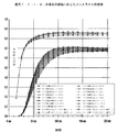
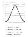
この関数は、点広がり関数(PSF)とも呼ばれている。その関数を当初は未だ決まっていない補正方法で使用可能とするためには、パラメータaとbを決めなければならない。そのために、様々な方法に基づき、所定のテストパターンによる照射を行なって、レジスト内のテストパターンにおける図形のCDを計測している。しかし、その場合、PSFの外に、別の影響を一緒に測定して、それにより、校正を実施している。
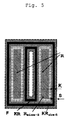
F 図形
K コントラストスタンプの幅
KR コントラストフレーム
KRsize-S KRを縮小した図形
R 残りの図形
Rsize-S Rを縮小した図形
S サイズ変更パラメータ
Claims (5)
- 補正アルゴリズムによる近接効果補正により、ウェーハ及びマスクの電子ビーム照射を制御する方法において、
幾何学的な手法により、コントラスト制御のための追加のコントラストフレーム(KR)と残りの図形(R)を全ての図形(F)に対して生成することと、
コントラストフレーム(KR)と残りの図形(R)の図形から、負のサイズ変更演算によって、より小さい図形(KRsize-SとRsize-S)を生成することと、
次に、照射量の割り当てによって、それらの図形(KR,R)の縁でレジスト閾値を達成するとの条件の下で、これらの図形(KRsize-SとRsize-S)を近接補正アルゴリズムに導入することと、
を特徴とする方法。 - 前記の幾何学的な手法が、
2×サイズ変更パラメータ(S)+コントラストスタンプの幅(K)の大きさによる負のサイズ変更演算によって、図形(F)から、残りの図形(R)を生成する工程と、
図形(F)からの残りの図形(R)の幾何学的な減算によって、コントラストフレーム(KR)を生成する工程と、
次に、サイズ変更パラメータ(S)の大きさによる負のサイズ変更演算によって、これらの得られた図形(RとKR)をKRsize-SとRsize-Sに縮小する工程と、
から構成されることを特徴とする請求項1に記載の方法。 - コントラストフレーム(KR)の全体の幅が、コントラストスタンプの幅(K)+2×サイズ変更パラメータ(S)であり、
ここで、
コントラストフレーム(KR)の幅<CDmin であり、
コントラストフレーム(KR)の幅の2倍<αの2.5倍であり、
全ての図形に対して、その幅<αの2.5倍であり、
これらの図形に最適な、照射量の補正を幾何学的に導き出す手法が自動的に得られる、
ことを特徴とする請求項1に記載の方法。 - 残りの図形(R)全体に対して、レジスト閾値を上回ることを保証するような照射量だけを割り当てるとの条件の下で、残りの図形(R)を近接補正アルゴリズムに導入することを特徴とする請求項1に記載の方法。
- 大きな図形内の小さな隙間(大きな図形内の切り取られた反転図形)を確実に検知するために、当初のパターンと色調値を逆転した反転パターンを同時に補正アルゴリズムに引き渡すとともに、それらのパターンを基本図形に分解する時及びそれらの基本図形に補正した照射量を割り当てる時に、両方の色調値を考慮することを特徴とする請求項1から4までのいずれか一つに記載の方法。
Applications Claiming Priority (3)
| Application Number | Priority Date | Filing Date | Title |
|---|---|---|---|
| DE102010004939A DE102010004939A1 (de) | 2010-01-18 | 2010-01-18 | Verfahren zur Steuerung der Elektronenstrahl-Belichtung von Wafern und Masken mit Proximity-Korrektur |
| DE102010004939.5 | 2010-01-18 | ||
| PCT/DE2011/000021 WO2011085719A1 (de) | 2010-01-18 | 2011-01-12 | Verfahren zur steuerung der elektronenstrahl-belichtung von wafern und masken mit proximity-korrektur |
Publications (2)
| Publication Number | Publication Date |
|---|---|
| JP2013517618A true JP2013517618A (ja) | 2013-05-16 |
| JP5622864B2 JP5622864B2 (ja) | 2014-11-12 |
Family
ID=43836665
Family Applications (1)
| Application Number | Title | Priority Date | Filing Date |
|---|---|---|---|
| JP2012548337A Active JP5622864B2 (ja) | 2010-01-18 | 2011-01-12 | 近接効果補正によるウェーハ及びマスクの電子ビーム照射制御方法 |
Country Status (7)
| Country | Link |
|---|---|
| US (1) | US8614052B2 (ja) |
| EP (1) | EP2526462B1 (ja) |
| JP (1) | JP5622864B2 (ja) |
| KR (1) | KR101747251B1 (ja) |
| CN (1) | CN102822742B (ja) |
| DE (2) | DE102010004939A1 (ja) |
| WO (1) | WO2011085719A1 (ja) |
Families Citing this family (10)
| Publication number | Priority date | Publication date | Assignee | Title |
|---|---|---|---|---|
| KR102403574B1 (ko) | 2014-02-21 | 2022-05-30 | 에이에스엠엘 네델란즈 비.브이. | 하전 입자 리소그래피 시스템에서의 근접 효과 보정 |
| KR102415201B1 (ko) | 2016-05-16 | 2022-06-29 | 노바-테크 엔지니어링, 엘엘씨 | 회전 포획 부재들을 갖는 가금류 주사 장치 및 사용 방법들 |
| US10534115B1 (en) * | 2017-09-22 | 2020-01-14 | Facebook Technologies, Llc | Gray-tone electron-beam lithography |
| US11220028B1 (en) | 2018-03-08 | 2022-01-11 | Facebook Technologies, Llc | Method of manufacture for thin, multi-bend optics by compression molding |
| US10976483B2 (en) | 2019-02-26 | 2021-04-13 | Facebook Technologies, Llc | Variable-etch-depth gratings |
| US11709422B2 (en) | 2020-09-17 | 2023-07-25 | Meta Platforms Technologies, Llc | Gray-tone lithography for precise control of grating etch depth |
| CN111965936B (zh) * | 2020-09-27 | 2022-06-07 | 湖南大学 | 大规模电子束曝光版图的高精度邻近效应快速矫正方法 |
| CN112987514B (zh) * | 2021-04-14 | 2022-02-01 | 湖南大学 | 一种基于二维快速傅里叶变换的电子束曝光的邻近效应矫正方法 |
| CN114660888B (zh) * | 2022-02-21 | 2025-04-18 | 上海华力集成电路制造有限公司 | 基于自由形式光源的快速制定adi的方法 |
| CN121721912A (zh) * | 2026-02-11 | 2026-03-24 | 华芯程(杭州)科技有限公司 | 边缘轮廓确定方法、掩膜版图修正方法、装置及电子设备 |
Citations (5)
| Publication number | Priority date | Publication date | Assignee | Title |
|---|---|---|---|---|
| JPS5984518A (ja) * | 1982-11-03 | 1984-05-16 | インタ−ナシヨナル ビジネス マシ−ンズ コ−ポレ−シヨン | 電子ビーム・リングラフィの近接効果補正方法 |
| JPS59208720A (ja) * | 1983-05-13 | 1984-11-27 | Hitachi Ltd | 描画方法および装置 |
| JPH02298019A (ja) * | 1989-05-12 | 1990-12-10 | Nippon Telegr & Teleph Corp <Ntt> | 電子ビーム描画装置 |
| JPH10144684A (ja) * | 1996-11-11 | 1998-05-29 | Nec Corp | 荷電粒子線描画方法及び装置 |
| JP2001168006A (ja) * | 1999-12-08 | 2001-06-22 | Nec Corp | パターンデータ処理方法及びプログラムを記憶した記憶媒体 |
Family Cites Families (7)
| Publication number | Priority date | Publication date | Assignee | Title |
|---|---|---|---|---|
| IL97022A0 (en) * | 1991-01-24 | 1992-03-29 | Ibm Israel | Partitioning method for e-beam lithography |
| DE4317899C2 (de) | 1993-05-28 | 1997-09-18 | Hans Eisenmann | Verfahren zur Abbildung mittels Elektronenstrahl-Lithographie |
| DE19818440C2 (de) | 1998-04-24 | 2002-10-24 | Pdf Solutions Gmbh | Verfahren zur Erzeugung von Daten für die Herstellung einer durch Entwurfsdaten definierten Struktur |
| KR100927454B1 (ko) * | 2003-10-31 | 2009-11-19 | 에이에스엠엘 마스크툴즈 비.브이. | 개선된 간섭 매핑 리소그래피를 이용하는 피처 최적화 |
| CN101228478B (zh) * | 2005-07-22 | 2012-08-08 | 富士通半导体股份有限公司 | 光掩模图形数据生成方法、用此数据生成的光掩模及用此掩模的半导体器件制造方法 |
| US7638247B2 (en) | 2006-06-22 | 2009-12-29 | Pdf Solutions, Inc. | Method for electron beam proximity effect correction |
| JP5082902B2 (ja) * | 2008-02-07 | 2012-11-28 | 富士通セミコンダクター株式会社 | フォトマスクの製造方法、フォトマスク製造装置及びフォトマスク |
-
2010
- 2010-01-18 DE DE102010004939A patent/DE102010004939A1/de not_active Withdrawn
-
2011
- 2011-01-12 KR KR1020127021739A patent/KR101747251B1/ko active Active
- 2011-01-12 WO PCT/DE2011/000021 patent/WO2011085719A1/de not_active Ceased
- 2011-01-12 JP JP2012548337A patent/JP5622864B2/ja active Active
- 2011-01-12 US US13/522,743 patent/US8614052B2/en active Active
- 2011-01-12 CN CN201180006436.6A patent/CN102822742B/zh not_active Expired - Fee Related
- 2011-01-12 EP EP11706145.7A patent/EP2526462B1/de active Active
- 2011-01-12 DE DE112011100264T patent/DE112011100264B4/de not_active Expired - Fee Related
Patent Citations (5)
| Publication number | Priority date | Publication date | Assignee | Title |
|---|---|---|---|---|
| JPS5984518A (ja) * | 1982-11-03 | 1984-05-16 | インタ−ナシヨナル ビジネス マシ−ンズ コ−ポレ−シヨン | 電子ビーム・リングラフィの近接効果補正方法 |
| JPS59208720A (ja) * | 1983-05-13 | 1984-11-27 | Hitachi Ltd | 描画方法および装置 |
| JPH02298019A (ja) * | 1989-05-12 | 1990-12-10 | Nippon Telegr & Teleph Corp <Ntt> | 電子ビーム描画装置 |
| JPH10144684A (ja) * | 1996-11-11 | 1998-05-29 | Nec Corp | 荷電粒子線描画方法及び装置 |
| JP2001168006A (ja) * | 1999-12-08 | 2001-06-22 | Nec Corp | パターンデータ処理方法及びプログラムを記憶した記憶媒体 |
Also Published As
| Publication number | Publication date |
|---|---|
| CN102822742A (zh) | 2012-12-12 |
| EP2526462A1 (de) | 2012-11-28 |
| JP5622864B2 (ja) | 2014-11-12 |
| KR20120116987A (ko) | 2012-10-23 |
| US8614052B2 (en) | 2013-12-24 |
| CN102822742B (zh) | 2015-05-20 |
| US20120293787A1 (en) | 2012-11-22 |
| WO2011085719A1 (de) | 2011-07-21 |
| KR101747251B1 (ko) | 2017-06-27 |
| DE102010004939A1 (de) | 2011-07-21 |
| DE112011100264B4 (de) | 2013-05-23 |
| EP2526462B1 (de) | 2013-11-27 |
| DE112011100264A5 (de) | 2012-11-08 |
Similar Documents
| Publication | Publication Date | Title |
|---|---|---|
| JP5622864B2 (ja) | 近接効果補正によるウェーハ及びマスクの電子ビーム照射制御方法 | |
| JP4476975B2 (ja) | 荷電粒子ビーム照射量演算方法、荷電粒子ビーム描画方法、プログラム及び荷電粒子ビーム描画装置 | |
| JP5063071B2 (ja) | パタン作成方法及び荷電粒子ビーム描画装置 | |
| JP6259694B2 (ja) | 荷電粒子ビーム描画装置及び荷電粒子ビームの照射量変調係数の取得方法 | |
| JPH04307723A (ja) | 電子ビーム・リソグラフィの近接効果補正方法 | |
| TWI652715B (zh) | 荷電粒子束描繪裝置及荷電粒子束描繪方法 | |
| JP6057635B2 (ja) | 荷電粒子ビーム描画装置及び荷電粒子ビーム描画方法 | |
| JP2018006748A (ja) | 表面上に書込む形状をバイアスするための方法およびシステム | |
| JP2009033025A (ja) | 荷電粒子ビーム描画装置におけるドーズ補正描画方法及び装置 | |
| JP2009194062A (ja) | 荷電粒子ビーム描画装置、パターンの寸法誤差補正装置及びパターンの寸法誤差補正方法 | |
| JP6767348B2 (ja) | ビームリソグラフィ用のプロセスドーズ量(Process Dose)とプロセスバイアス(Process Bias)の決定(Determination) | |
| JP2012182506A (ja) | パタン作成方法及び荷電粒子ビーム描画装置 | |
| JP2010250286A (ja) | フォトマスク、半導体装置、荷電ビーム描画装置 | |
| JP2012212792A (ja) | 荷電粒子ビーム描画装置及び荷電粒子ビーム描画方法 | |
| US11443918B2 (en) | Charged particle beam writing method and charged particle beam writing apparatus | |
| KR20220134469A (ko) | 마스크 결함을 수리하기 위한 방법, 장치 및 컴퓨터 프로그램 | |
| Kim et al. | Improving CD uniformity using MB-MDP for 14nm node and beyond | |
| JP2009259992A (ja) | 電子線描画用パターンデータの作成方法及びそれに用いる近接効果補正方法、そのデータを用いたパターン形成方法 | |
| JP2010219285A (ja) | 荷電粒子ビーム描画方法および荷電粒子ビーム描画装置 | |
| JPWO2012035892A1 (ja) | 描画方法及び描画装置 | |
| JP6167663B2 (ja) | 現像ローディング補正プログラム、計算機、描画システム、現像ローディング補正方法 | |
| Lee et al. | The requirements for the future e-beam mask writer: statistical analysis of pattern accuracy | |
| JP2012023279A (ja) | 荷電粒子ビーム描画装置及び荷電粒子ビーム描画方法 | |
| JP2012069667A (ja) | 荷電粒子ビーム描画装置及び荷電粒子ビーム描画方法 | |
| JP5871557B2 (ja) | 荷電粒子ビーム描画装置及び荷電粒子ビーム描画方法 |
Legal Events
| Date | Code | Title | Description |
|---|---|---|---|
| A977 | Report on retrieval |
Free format text: JAPANESE INTERMEDIATE CODE: A971007 Effective date: 20131024 |
|
| A131 | Notification of reasons for refusal |
Free format text: JAPANESE INTERMEDIATE CODE: A131 Effective date: 20131126 |
|
| A601 | Written request for extension of time |
Free format text: JAPANESE INTERMEDIATE CODE: A601 Effective date: 20140220 |
|
| A602 | Written permission of extension of time |
Free format text: JAPANESE INTERMEDIATE CODE: A602 Effective date: 20140227 |
|
| A521 | Request for written amendment filed |
Free format text: JAPANESE INTERMEDIATE CODE: A523 Effective date: 20140324 |
|
| TRDD | Decision of grant or rejection written | ||
| A01 | Written decision to grant a patent or to grant a registration (utility model) |
Free format text: JAPANESE INTERMEDIATE CODE: A01 Effective date: 20140903 |
|
| A61 | First payment of annual fees (during grant procedure) |
Free format text: JAPANESE INTERMEDIATE CODE: A61 Effective date: 20140922 |
|
| R150 | Certificate of patent or registration of utility model |
Ref document number: 5622864 Country of ref document: JP Free format text: JAPANESE INTERMEDIATE CODE: R150 |
|
| S111 | Request for change of ownership or part of ownership |
Free format text: JAPANESE INTERMEDIATE CODE: R313113 |
|
| R350 | Written notification of registration of transfer |
Free format text: JAPANESE INTERMEDIATE CODE: R350 |
|
| R250 | Receipt of annual fees |
Free format text: JAPANESE INTERMEDIATE CODE: R250 |
|
| R250 | Receipt of annual fees |
Free format text: JAPANESE INTERMEDIATE CODE: R250 |
|
| R250 | Receipt of annual fees |
Free format text: JAPANESE INTERMEDIATE CODE: R250 |
|
| R250 | Receipt of annual fees |
Free format text: JAPANESE INTERMEDIATE CODE: R250 |
|
| R250 | Receipt of annual fees |
Free format text: JAPANESE INTERMEDIATE CODE: R250 |
|
| R250 | Receipt of annual fees |
Free format text: JAPANESE INTERMEDIATE CODE: R250 |
|
| R250 | Receipt of annual fees |
Free format text: JAPANESE INTERMEDIATE CODE: R250 |
|
| R250 | Receipt of annual fees |
Free format text: JAPANESE INTERMEDIATE CODE: R250 |
|
| R250 | Receipt of annual fees |
Free format text: JAPANESE INTERMEDIATE CODE: R250 |