JP2013517618A - Wafer and mask electron beam irradiation control method by proximity effect correction - Google Patents
Wafer and mask electron beam irradiation control method by proximity effect correction Download PDFInfo
- Publication number
- JP2013517618A JP2013517618A JP2012548337A JP2012548337A JP2013517618A JP 2013517618 A JP2013517618 A JP 2013517618A JP 2012548337 A JP2012548337 A JP 2012548337A JP 2012548337 A JP2012548337 A JP 2012548337A JP 2013517618 A JP2013517618 A JP 2013517618A
- Authority
- JP
- Japan
- Prior art keywords
- figures
- size
- contrast
- remaining
- correction
- Prior art date
- Legal status (The legal status is an assumption and is not a legal conclusion. Google has not performed a legal analysis and makes no representation as to the accuracy of the status listed.)
- Granted
Links
Images
Classifications
-
- G—PHYSICS
- G03—PHOTOGRAPHY; CINEMATOGRAPHY; ANALOGOUS TECHNIQUES USING WAVES OTHER THAN OPTICAL WAVES; ELECTROGRAPHY; HOLOGRAPHY
- G03F—PHOTOMECHANICAL PRODUCTION OF TEXTURED OR PATTERNED SURFACES, e.g. FOR PRINTING, FOR PROCESSING OF SEMICONDUCTOR DEVICES; MATERIALS THEREFOR; ORIGINALS THEREFOR; APPARATUS SPECIALLY ADAPTED THEREFOR
- G03F7/00—Photomechanical, e.g. photolithographic, production of textured or patterned surfaces, e.g. printing surfaces; Materials therefor, e.g. comprising photoresists; Apparatus specially adapted therefor
- G03F7/20—Exposure; Apparatus therefor
-
- H—ELECTRICITY
- H01—ELECTRIC ELEMENTS
- H01J—ELECTRIC DISCHARGE TUBES OR DISCHARGE LAMPS
- H01J37/00—Discharge tubes with provision for introducing objects or material to be exposed to the discharge, e.g. for the purpose of examination or processing thereof
- H01J37/30—Electron-beam or ion-beam tubes for localised treatment of objects
- H01J37/317—Electron-beam or ion-beam tubes for localised treatment of objects for changing properties of the objects or for applying thin layers thereon, e.g. for ion implantation
- H01J37/3174—Particle-beam lithography, e.g. electron beam lithography
-
- B—PERFORMING OPERATIONS; TRANSPORTING
- B82—NANOTECHNOLOGY
- B82Y—SPECIFIC USES OR APPLICATIONS OF NANOSTRUCTURES; MEASUREMENT OR ANALYSIS OF NANOSTRUCTURES; MANUFACTURE OR TREATMENT OF NANOSTRUCTURES
- B82Y10/00—Nanotechnology for information processing, storage or transmission, e.g. quantum computing or single electron logic
-
- B—PERFORMING OPERATIONS; TRANSPORTING
- B82—NANOTECHNOLOGY
- B82Y—SPECIFIC USES OR APPLICATIONS OF NANOSTRUCTURES; MEASUREMENT OR ANALYSIS OF NANOSTRUCTURES; MANUFACTURE OR TREATMENT OF NANOSTRUCTURES
- B82Y40/00—Manufacture or treatment of nanostructures
-
- G—PHYSICS
- G03—PHOTOGRAPHY; CINEMATOGRAPHY; ANALOGOUS TECHNIQUES USING WAVES OTHER THAN OPTICAL WAVES; ELECTROGRAPHY; HOLOGRAPHY
- G03F—PHOTOMECHANICAL PRODUCTION OF TEXTURED OR PATTERNED SURFACES, e.g. FOR PRINTING, FOR PROCESSING OF SEMICONDUCTOR DEVICES; MATERIALS THEREFOR; ORIGINALS THEREFOR; APPARATUS SPECIALLY ADAPTED THEREFOR
- G03F1/00—Originals for photomechanical production of textured or patterned surfaces, e.g., masks, photo-masks, reticles; Mask blanks or pellicles therefor; Containers specially adapted therefor; Preparation thereof
- G03F1/68—Preparation processes not covered by groups G03F1/20 - G03F1/50
- G03F1/70—Adapting basic layout or design of masks to lithographic process requirements, e.g., second iteration correction of mask patterns for imaging
-
- G—PHYSICS
- G03—PHOTOGRAPHY; CINEMATOGRAPHY; ANALOGOUS TECHNIQUES USING WAVES OTHER THAN OPTICAL WAVES; ELECTROGRAPHY; HOLOGRAPHY
- G03F—PHOTOMECHANICAL PRODUCTION OF TEXTURED OR PATTERNED SURFACES, e.g. FOR PRINTING, FOR PROCESSING OF SEMICONDUCTOR DEVICES; MATERIALS THEREFOR; ORIGINALS THEREFOR; APPARATUS SPECIALLY ADAPTED THEREFOR
- G03F1/00—Originals for photomechanical production of textured or patterned surfaces, e.g., masks, photo-masks, reticles; Mask blanks or pellicles therefor; Containers specially adapted therefor; Preparation thereof
- G03F1/68—Preparation processes not covered by groups G03F1/20 - G03F1/50
- G03F1/76—Patterning of masks by imaging
- G03F1/78—Patterning of masks by imaging by charged particle beam [CPB], e.g. electron beam patterning of masks
-
- H—ELECTRICITY
- H01—ELECTRIC ELEMENTS
- H01J—ELECTRIC DISCHARGE TUBES OR DISCHARGE LAMPS
- H01J37/00—Discharge tubes with provision for introducing objects or material to be exposed to the discharge, e.g. for the purpose of examination or processing thereof
- H01J37/30—Electron-beam or ion-beam tubes for localised treatment of objects
- H01J37/317—Electron-beam or ion-beam tubes for localised treatment of objects for changing properties of the objects or for applying thin layers thereon, e.g. for ion implantation
Landscapes
- Engineering & Computer Science (AREA)
- Chemical & Material Sciences (AREA)
- Physics & Mathematics (AREA)
- Nanotechnology (AREA)
- General Physics & Mathematics (AREA)
- Crystallography & Structural Chemistry (AREA)
- Analytical Chemistry (AREA)
- Plasma & Fusion (AREA)
- Mathematical Physics (AREA)
- Theoretical Computer Science (AREA)
- Condensed Matter Physics & Semiconductors (AREA)
- Manufacturing & Machinery (AREA)
- Electron Beam Exposure (AREA)
- Exposure And Positioning Against Photoresist Photosensitive Materials (AREA)
Abstract
【課題】 本発明は、ウェーハ及びマスクを製造するための電子ビームリソグラフィ方法に関する。邪魔をする近接効果の作用を低減するために、より正確な補正を可能とする、電子ビームを制御するための拡張した補正アルゴリズムを採用する。そのため、本発明の課題は、一つのパターンの全ての図形のコントラストとCDを最適に制御できる改善された補正方法を提供することである。本発明では、幾何学的な手法により、コントラスト制御のための追加のコントラストフレーム(KR)と残りの図形(R)を全ての図形(F)に対して生成し、次に、コントラストフレーム(KR)と残りの図形(R)の図形から、負のサイズ変更演算によって、より小さい図形(KRsize-SとRsize-S)を生成し、次に、照射量の割り当てによって、それらの図形(KR,R)の縁でレジスト閾値を達成するとの条件により、これらの図形(KRsize-SとRsize-S)を近接補正アルゴリズムに導入することによって、この課題を解決している。The present invention relates to an electron beam lithography method for manufacturing a wafer and a mask. In order to reduce the effects of disturbing proximity effects, an extended correction algorithm for controlling the electron beam that allows more accurate correction is employed. Therefore, an object of the present invention is to provide an improved correction method capable of optimally controlling the contrast and CD of all figures in one pattern. In the present invention, an additional contrast frame (KR) and the remaining figure (R) for contrast control are generated for all figures (F) by a geometric method, and then the contrast frame (KR) is generated. ) And the remaining figure (R) by a negative resize operation to generate smaller figures (KR size-S and R size-S ), and then assign those doses by assigning dose ( This problem is solved by introducing these figures (KR size-S and R size-S ) into the proximity correction algorithm under the condition that the resist threshold is achieved at the edge of KR, R).
Description
本発明は、ウェーハ及びマスクを製造するための電子ビームリソグラフィ方法に関する。邪魔をする近接効果の作用を低減するために、より正確な補正を可能とする、電子ビームを制御するための拡張した補正アルゴリズムを採用する。 The present invention relates to an electron beam lithography method for manufacturing wafers and masks. In order to reduce the effects of disturbing proximity effects, an extended correction algorithm for controlling the electron beam that allows more accurate correction is employed.
電子ビーム照射設備を用いたパターン生成方法は、ずっと前から周知である。所要のパターンを小さい基本図形に分解して、感光性のラッカー層の上に投影する。レジストを成長させた後、そのパターンを出来る限り正確にレジストに投影している。所定の形状の電子ビーム(ガウス分布ビーム、フォームビーム或いはマルチピクセルビーム)をレジストに照射することによって、電子ビームの照射量分布と一致しない照射量分布がレジストに形成されている。その原因は、レジストと基板の原子又は分子による電子の散乱である。それは、近接効果と呼ばれている。 A pattern generation method using an electron beam irradiation facility has been known for a long time. The required pattern is broken down into small basic figures and projected onto the photosensitive lacquer layer. After growing the resist, the pattern is projected onto the resist as accurately as possible. By irradiating the resist with an electron beam having a predetermined shape (Gaussian distribution beam, foam beam, or multi-pixel beam), a dose distribution that does not match the dose distribution of the electron beam is formed on the resist. The cause is scattering of electrons by atoms or molecules of the resist and the substrate. It is called the proximity effect.
この場合、到達範囲が短い効果(約20nm〜40nm、前方散乱)と到達範囲が明らかに長い効果(約5,000nm〜30,000nm、後方散乱)が発生する。その結果、電子ビームの拡大(照射量分布の乱れ)及び異なる基本図形の照射量分布の相互の影響が起こり、そのため、結局のところ、全ての所望の基本図形を同じ照射量及び変わらない幾何学形状で照射した場合、レジストに生じる照射量分布が歪曲されて、レジストに生成される構造が所望のパターンのCDを持たなくなる。従って、生成されたパターンは、通常所望の目的に使用できない。そのような効果を補正可能とするためには、先ず近接効果に関する数学モデルを設定しなければならない。 In this case, an effect with a short reach (about 20 nm to 40 nm, forward scattering) and an effect with a clearly long reach (about 5,000 nm to 30,000 nm, backscatter) occur. As a result, electron beam expansion (irradiation dose disorder) and the mutual influence of different basic figure dose distributions occur, so that eventually all desired basic figures have the same dose and unchanged geometry. When irradiated in a shape, the dose distribution generated in the resist is distorted, and the structure generated in the resist does not have a desired pattern of CD. Thus, the generated pattern cannot usually be used for the desired purpose. In order to be able to correct such an effect, a mathematical model relating to the proximity effect must first be set.
二つのガウス関数を重ね合わせることによって、その効果を規定できることが広く認識されており(数式1参照)、αとβは前方散乱と後方散乱の到達範囲を表し、ηはそれらの効果の大きさの比率を表している。 It is widely recognized that the effect can be defined by superimposing two Gaussian functions (see Equation 1), α and β represent the reach of forward and backscattering, and η is the magnitude of these effects Represents the ratio.
数式1:
この関数は、点広がり関数(PSF)とも呼ばれている。その関数を当初は未だ決まっていない補正方法で使用可能とするためには、パラメータaとbを決めなければならない。そのために、様々な方法に基づき、所定のテストパターンによる照射を行なって、レジスト内のテストパターンにおける図形のCDを計測している。しかし、その場合、PSFの外に、別の影響を一緒に測定して、それにより、校正を実施している。
Formula 1:
This function is also called a point spread function (PSF). In order to be able to use the function in a correction method that has not yet been determined, the parameters a and b must be determined. For this purpose, irradiation with a predetermined test pattern is performed based on various methods, and the figure CD in the test pattern in the resist is measured. However, in that case, besides PSF, another effect is measured together, thereby performing calibration.
それは、特に、電子相互のクーロン相互作用と、電磁投影システムのレンズの収差と、照射と成長時のレジストの化学反応で引き起こされる効果とによる所謂ビームのぼやけである。そのため、以下において、そのようなプロセス全体を通じて校正された関数は、「プロセス近接効果関数(PPF)」と称する。PPFを定義するために、三つ以上のガウス関数を重ね合わせることが必要な場合が有る。 It is a so-called beam blurring, in particular due to electron-Coulomb interaction, lens aberrations of the electromagnetic projection system, and effects caused by the chemical reaction of the resist during irradiation and growth. Therefore, in the following, a function calibrated throughout such a process is referred to as a “process proximity effect function (PPF)”. In order to define a PPF, it may be necessary to superimpose three or more Gaussian functions.
そして、その結果得られる照射量分布は、PPFとパターン自体の畳み込み演算の結果として算出することができる。容易に納得できる通り、その関数は、放射形対称であり、位置の依存せず、外側に向かって単調に低下して行く。 The dose distribution obtained as a result can be calculated as a result of the convolution calculation of the PPF and the pattern itself. As can be readily appreciated, the function is radially symmetric and is monotonically decreasing outward without position dependence.
電子ビームリソグラフィによって生成されるレジストパターンを使用可能とするためには、(物理的な理由から)避けられない近接効果を補正しなければならない。電子ビームの照射量制御をサポートする電子ビーム照射設備では、通常その間にパターンの図形を小さい図形に細分して、場合によっては、そのような小さい図形に対して、個々の照射量を計算し、プロセス全体(レジストの照射と成長)の実行後に、パターンの図形が所望のCDを持つような措置が取られている。 In order to be able to use resist patterns produced by electron beam lithography, the inevitable proximity effect (for physical reasons) must be corrected. In electron beam irradiation equipment that supports electron beam irradiation control, the pattern figure is usually subdivided into small figures during that period, and in some cases, individual irradiation doses are calculated for such small figures, After the entire process (resist irradiation and growth) is performed, measures are taken so that the pattern figure has the desired CD.
任意のパターンに適した、照射量又は幾何学形状を補正する方法が特許文献1に記載されており、商業的に入手可能な周知のソフトウェアPROXECCOに実装されている。その方法は、「好適なフーリエ変換による展開」の数学的な方法をベースとしており、以下において、短く「展開」と称する。別の方法は、特許文献2に開示されている。
A method for correcting an irradiation dose or a geometric shape suitable for an arbitrary pattern is described in
従来技術に対応する全ての補正方法は、幾つかの問題に苦しんでいる。我々に周知の近接効果補正方法は、パターン内の図形のCDがPPFのαパラメータの約1.3倍よりも大きい場合(非特許文献1参照)にしか満足に機能しない。しかし、半導体技術の現在の技術水準は、約35nmのCDを求めており、2016年1月までに更に22nmのCDを求めている(ITRSロードマップ)。現在入手可能な、半導体製造で使用可能な(特に、一つのプロセスに付随するレジストによる)リソグラフィプロセスは、約25〜30nmのαパラメータを有する、即ち、下方には約38〜45nmまでの直接照射しか可能ではない。如何にして、既存のプロセスに関する投影品質を一層改善するかに関する一連の提案が知られている(例えば、特許文献3参照)。これらの補正を改善するための全ての提案は、「展開」に基づく補正アルゴリズムの修正を目指しており、これまで大きな品質の改善を実現していない。 All correction methods corresponding to the prior art suffer from several problems. The proximity effect correction method known to us works satisfactorily only when the figure CD in the pattern is larger than about 1.3 times the α parameter of PPF (see Non-Patent Document 1). However, the current technological level of semiconductor technology requires a CD of about 35 nm, and by January 2016, a CD of 22 nm is further required (ITRS roadmap). Currently available, lithographic processes that can be used in semiconductor manufacturing (especially with resists associated with one process) have an alpha parameter of about 25-30 nm, ie direct irradiation down to about 38-45 nm. Only possible. A series of proposals regarding how to further improve the projection quality related to existing processes is known (see, for example, Patent Document 3). All the proposals for improving these corrections aim to modify the correction algorithm based on “development” and have not realized a significant quality improvement so far.
以上のことから、本発明の課題は、一つのパターンの全ての図形のコントラストとCDを最適に制御できる改善された補正方法を提供することである。 In view of the above, an object of the present invention is to provide an improved correction method capable of optimally controlling the contrast and CD of all figures in one pattern.
別の課題は、そのような補正方法を所定の周知の補正アルゴリズムとPPFの規定形態に関係無い形で構成することである。 Another problem is to configure such a correction method in a form that is not related to a predetermined well-known correction algorithm and the prescribed form of PPF.
本課題は、本発明による請求項1の特徴により解決される。
This problem is solved by the features of
この新しい方法は、以下の考えと知見に基づいている。 This new method is based on the following ideas and findings.
近接効果のモデルから、非常に特殊なパターンに対して、近接効果の補正を数学的な「展開」機構無しに算出できるとの結果が得られている。そのパターンは、一つの面の二つの次元に無限に延びる、等間隔の線と隙間から成る見本である。 The result of the proximity effect model shows that the proximity effect correction can be calculated for a very special pattern without a mathematical “development” mechanism. The pattern is a sample of equally spaced lines and gaps extending indefinitely in the two dimensions of a surface.
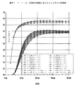
照射量を計算した場合、直線の図形に関する比較的正しい照射量が、線の幅にも具体的なPPFにも関係無く、常に1.0と等しいことが分かった。ここで、その結果として得られる照射量分布(非特許文献1と2)を計算するために(即ち、照射量分布をシミュレーションするために)、任意のPPFを使用した場合(これは、数学的な展開機構が無くとも可能である)、αパラメータの約0.65倍で初めてレジストのコントラストが最終的に消え去ることが分かった(図1参照)。
When calculating the dose, it was found that the relatively correct dose for a straight line figure was always equal to 1.0, regardless of the line width or the specific PPF. Here, in order to calculate the resulting dose distribution (
即ち、密な線のパターンを仮定すると、如何なる場合でも、それより小さい構造を投影することができない。しかし、実際には、αパラメータの約1.3倍の場合に既に投影限界に達していると、実験が示している(非特許文献1)。しかし、(その結果が両方に関係無く正しいと見做されているために)補正も校正も間違っている可能性が有るので、PPFの別の補正アルゴリズム又は校正によって、その範囲での投影の改善を実現しようとする全ての試みも、必ず失敗すると判断しなければならない。 That is, assuming a dense line pattern, a smaller structure cannot be projected in any case. However, in practice, experiments have shown that the projection limit has already been reached when the parameter is about 1.3 times the α parameter (Non-Patent Document 1). However, since correction and calibration may be wrong (because the result is considered correct regardless of both), another correction algorithm or calibration of PPF can improve projection in that range. It must be determined that all attempts to achieve this will fail.
この問題の原因は、全ての周知の方法が、投影後の図形のCDの制御によって、「正しい」CD、即ち、投影前のCDを実現すること(CD制御)を追求していることに有る。前記のαの約0.65倍〜αの1.3倍の範囲において、CD制御は不十分であり、コントラスト制御によって補完しなければならない。パターンのコントラスト(投影パターンのデータでは、「図形」と「隙間」の間のコントラストは常に1.0に等しい)を実現できなかった場合でも、実現可能なコントラストの最大化を実行して、当該の範囲での投影を実現しなければならない。 The cause of this problem is that all known methods seek to achieve a “correct” CD, ie, a CD before projection (CD control) by controlling the CD of the projected figure. . In the range of about 0.65 times α to 1.3 times α, CD control is insufficient and must be supplemented by contrast control. Even if the contrast of the pattern (in the projection pattern data, the contrast between “figure” and “gap” is always equal to 1.0) cannot be realized, the maximum possible contrast is executed, Projection in the range of
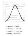
そのため、幾何学的に導き出す照射量補正方法を導入する。その場合、コントラストの制御は、サイズ変更パラメータSによって決まる(図2参照)。 Therefore, a dose correction method derived geometrically is introduced. In this case, the contrast control is determined by the size change parameter S (see FIG. 2).
この場合、サイズ変更演算によって、xとy方向における図形の大きさをそれぞれ大きさS(例えば、10nm)だけ縮小する。次に、補正のためにPPFを使用する照射プロセスが照射時に正確に当初の図形の線幅を生成するように、図形に割り当てる照射量を補正する。図2の曲線は、実際に線幅が常に等しいが、サイズ変更パラメータが大きくなると、レジスト閾値の位置でのコントラスト、特に、コントラストの勾配が同様に大きくなることを示している。 In this case, the size of the figure in the x and y directions is reduced by the size S (for example, 10 nm) by the size change calculation. Next, the irradiation dose assigned to the graphic is corrected so that the irradiation process using PPF for correction generates the line width of the original graphic accurately at the time of irradiation. The curves in FIG. 2 show that the line widths are always always equal, but the contrast at the resist threshold position, in particular the contrast gradient, increases as the sizing parameter increases.
この方法は、同じ線幅の図形から成るテストパターンでは明らかに良好に機能するが、一般的なパターンのコントラスト制御に対しては未だ不十分である。一般的なパターンには、所定の大きさの図形だけでなく、多くの図形が混ざったものも含まれている。 This method clearly works well for test patterns consisting of figures with the same line width, but is still insufficient for contrast control of general patterns. The general pattern includes not only a figure of a predetermined size but also a mixture of many figures.
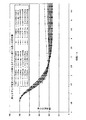
今では、全てのPFFに関して、図形の幅に応じて、コントラストに一つの転換点が存在することを発見した。それは、PPFのαパラメータの約2.5倍の所に有る(図3参照)。 Now, for all PFFs, we have found that there is one turning point in contrast, depending on the width of the figure. It is about 2.5 times the α parameter of PPF (see FIG. 3).
そのような物理的な実態の知見から、この新しい方法の工程が導き出される。この場合、コントラストスタンプの幅のパラメータKを更に導入していることが重要である。 From this knowledge of the physical reality, the steps of this new method are derived. In this case, it is important to further introduce a parameter K for the width of the contrast stamp.
この請求項1に記載の新しい方法は、電子ビームの照射時のコントラストとCDを同時に制御することによって、一つのパターンの全ての図形の高い投影精度を可能としている。
The new method according to
本方法の幾つかの工程に関する更に別の有利な変化形態は、従属請求項2〜4に記載されている。
Further advantageous variants for some steps of the method are described in the
従属請求項5には、大きな図形内の小さな隙間を見分けることが可能な本方法の変化形態が提示されている。そのため、補正アルゴリズムの実行時の小さな隙間の見過ごしが防止される。
The
以下において、一つの例により本方法を説明する。 In the following, the method will be described by way of an example.
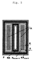
図4の線状の隙間を切り取った四角形の形状の図形Fは、一つのパターンの任意の複雑な図形に対する見本としての役割を果たしている。第一の演算では、Fから、残りの図形Rを生成する。それは、(2×S+K)の大きさによる負のサイズ変更演算によって実行される。コントラストフレームKRは、図形Fからの残りの図形Rの幾何学的な減算(KR=F\R)によって生成される。 The quadrangular figure F from which the linear gaps in FIG. 4 are cut serves as a sample for an arbitrarily complex figure of one pattern. In the first calculation, the remaining graphic R is generated from F. It is performed by a negative resize operation with a size of (2 × S + K). The contrast frame KR is generated by geometric subtraction of the remaining figure R from the figure F (KR = F \ R).
ここで得られた図形のコントラストフレームKRと残りの図形Rは、それぞれSの大きさによる負のサイズ変更演算によって、KRsize-SとRsize-Sに縮小される。そして、KRsize-SとRsize-Sは、図形KRの縁でレジスト閾値を正確に達成するとともに、図形Rの領域でレジスト閾値を上回ることを保証するように、それぞれ照射量を割り当てるとの条件の下で、一緒に近接効果補正アルゴリズムに引き渡される。 The contrast frame KR of the figure obtained here and the remaining figure R are reduced to KR size-S and R size-S by a negative size change operation based on the size of S, respectively. KR size-S and R size-S are respectively assigned doses so as to accurately achieve the resist threshold at the edge of the graphic KR and to ensure that the resist threshold is exceeded in the region of the graphic R. Under the condition, it is handed over to the proximity effect correction algorithm together.
CD 構造幅
F 図形
K コントラストスタンプの幅
KR コントラストフレーム
KRsize-S KRを縮小した図形
R 残りの図形
Rsize-S Rを縮小した図形
S サイズ変更パラメータ
CD structure width F figure K contrast stamp width KR contrast frame KR size-S KR reduced figure R remaining figure R size-S R reduced figure S resize parameter
数式1:
Formula 1:
Claims (5)
幾何学的な手法により、コントラスト制御のための追加のコントラストフレーム(KR)と残りの図形(R)を全ての図形(F)に対して生成することと、
コントラストフレーム(KR)と残りの図形(R)の図形から、負のサイズ変更演算によって、より小さい図形(KRsize-SとRsize-S)を生成することと、
次に、照射量の割り当てによって、それらの図形(KR,R)の縁でレジスト閾値を達成するとの条件の下で、これらの図形(KRsize-SとRsize-S)を近接補正アルゴリズムに導入することと、
を特徴とする方法。 In a method of controlling electron beam irradiation of a wafer and a mask by proximity effect correction by a correction algorithm,
Generating an additional contrast frame (KR) for contrast control and the remaining figure (R) for all figures (F) by geometric techniques;
Generating smaller graphics (KR size-S and R size-S ) from the contrast frame (KR) and the remaining graphics (R) by negative resizing operations;
Next, these figures (KR size-S and R size-S ) are used as proximity correction algorithms under the condition that the resist threshold is achieved at the edges of the figures (KR, R) by assigning the dose. Introducing it,
A method characterized by.
2×サイズ変更パラメータ(S)+コントラストスタンプの幅(K)の大きさによる負のサイズ変更演算によって、図形(F)から、残りの図形(R)を生成する工程と、
図形(F)からの残りの図形(R)の幾何学的な減算によって、コントラストフレーム(KR)を生成する工程と、
次に、サイズ変更パラメータ(S)の大きさによる負のサイズ変更演算によって、これらの得られた図形(RとKR)をKRsize-SとRsize-Sに縮小する工程と、
から構成されることを特徴とする請求項1に記載の方法。 The geometric method is
Generating a remaining graphic (R) from the graphic (F) by a negative sizing operation based on the size of 2 × resizing parameter (S) + contrast stamp width (K);
Generating a contrast frame (KR) by geometric subtraction of the remaining figure (R) from figure (F);
Next, a step of reducing these obtained figures (R and KR) to KR size-S and R size-S by a negative resize operation according to the size of the resize parameter (S);
The method of claim 1, comprising:
ここで、
コントラストフレーム(KR)の幅<CDmin であり、
コントラストフレーム(KR)の幅の2倍<αの2.5倍であり、
全ての図形に対して、その幅<αの2.5倍であり、
これらの図形に最適な、照射量の補正を幾何学的に導き出す手法が自動的に得られる、
ことを特徴とする請求項1に記載の方法。 The overall width of the contrast frame (KR) is the width of the contrast stamp (K) + 2 × resize parameter (S),
here,
The width of the contrast frame (KR) <CD min ,
2 times the width of the contrast frame (KR) <2.5 times α,
For all figures, its width <2.5 times α,
A method of geometrically deriving dose correction that is optimal for these figures is automatically obtained.
The method according to claim 1.
Applications Claiming Priority (3)
| Application Number | Priority Date | Filing Date | Title |
|---|---|---|---|
| DE102010004939A DE102010004939A1 (en) | 2010-01-18 | 2010-01-18 | Method for controlling the electron beam exposure of wafers and masks with proximity correction |
| DE102010004939.5 | 2010-01-18 | ||
| PCT/DE2011/000021 WO2011085719A1 (en) | 2010-01-18 | 2011-01-12 | Method for controlling the electron beam exposure of wafers and masks using proximity correction |
Publications (2)
| Publication Number | Publication Date |
|---|---|
| JP2013517618A true JP2013517618A (en) | 2013-05-16 |
| JP5622864B2 JP5622864B2 (en) | 2014-11-12 |
Family
ID=43836665
Family Applications (1)
| Application Number | Title | Priority Date | Filing Date |
|---|---|---|---|
| JP2012548337A Active JP5622864B2 (en) | 2010-01-18 | 2011-01-12 | Wafer and mask electron beam irradiation control method by proximity effect correction |
Country Status (7)
| Country | Link |
|---|---|
| US (1) | US8614052B2 (en) |
| EP (1) | EP2526462B1 (en) |
| JP (1) | JP5622864B2 (en) |
| KR (1) | KR101747251B1 (en) |
| CN (1) | CN102822742B (en) |
| DE (2) | DE102010004939A1 (en) |
| WO (1) | WO2011085719A1 (en) |
Families Citing this family (10)
| Publication number | Priority date | Publication date | Assignee | Title |
|---|---|---|---|---|
| KR102403574B1 (en) | 2014-02-21 | 2022-05-30 | 에이에스엠엘 네델란즈 비.브이. | Proximity effect correction in a charged particle lithography system |
| KR102415201B1 (en) | 2016-05-16 | 2022-06-29 | 노바-테크 엔지니어링, 엘엘씨 | Poultry Injection Devices and Methods of Use With Rotating Capture Members |
| US10534115B1 (en) * | 2017-09-22 | 2020-01-14 | Facebook Technologies, Llc | Gray-tone electron-beam lithography |
| US11220028B1 (en) | 2018-03-08 | 2022-01-11 | Facebook Technologies, Llc | Method of manufacture for thin, multi-bend optics by compression molding |
| US10976483B2 (en) | 2019-02-26 | 2021-04-13 | Facebook Technologies, Llc | Variable-etch-depth gratings |
| US11709422B2 (en) | 2020-09-17 | 2023-07-25 | Meta Platforms Technologies, Llc | Gray-tone lithography for precise control of grating etch depth |
| CN111965936B (en) * | 2020-09-27 | 2022-06-07 | 湖南大学 | A Fast Correction Method of High Precision Proximity Effect for Large Scale Electron Beam Exposure Layout |
| CN112987514B (en) * | 2021-04-14 | 2022-02-01 | 湖南大学 | Two-dimensional fast Fourier transform-based proximity effect correction method for electron beam exposure |
| CN114660888B (en) * | 2022-02-21 | 2025-04-18 | 上海华力集成电路制造有限公司 | A method for rapid formulation of ADI based on free-form light sources |
| CN121721912A (en) * | 2026-02-11 | 2026-03-24 | 华芯程(杭州)科技有限公司 | Edge contour determination method, mask layout correction device and electronic equipment |
Citations (5)
| Publication number | Priority date | Publication date | Assignee | Title |
|---|---|---|---|---|
| JPS5984518A (en) * | 1982-11-03 | 1984-05-16 | インタ−ナシヨナル ビジネス マシ−ンズ コ−ポレ−シヨン | Method of approaching and correcting electronic beam lithography |
| JPS59208720A (en) * | 1983-05-13 | 1984-11-27 | Hitachi Ltd | Drawing method and apparatus |
| JPH02298019A (en) * | 1989-05-12 | 1990-12-10 | Nippon Telegr & Teleph Corp <Ntt> | Electron-beam drawing apparatus |
| JPH10144684A (en) * | 1996-11-11 | 1998-05-29 | Nec Corp | Charged particle beam writing method and apparatus therefor |
| JP2001168006A (en) * | 1999-12-08 | 2001-06-22 | Nec Corp | Pattern data processing method and storage medium storing program |
Family Cites Families (7)
| Publication number | Priority date | Publication date | Assignee | Title |
|---|---|---|---|---|
| IL97022A0 (en) * | 1991-01-24 | 1992-03-29 | Ibm Israel | Partitioning method for e-beam lithography |
| DE4317899C2 (en) | 1993-05-28 | 1997-09-18 | Hans Eisenmann | Process for imaging using electron beam lithography |
| DE19818440C2 (en) | 1998-04-24 | 2002-10-24 | Pdf Solutions Gmbh | Method for generating data for the production of a structure defined by design data |
| KR100927454B1 (en) * | 2003-10-31 | 2009-11-19 | 에이에스엠엘 마스크툴즈 비.브이. | Feature Optimization with Enhanced Interference Mapping Lithography |
| CN101228478B (en) * | 2005-07-22 | 2012-08-08 | 富士通半导体股份有限公司 | Photomask pattern data generation method, photomask generated using the data, and semiconductor device manufacturing method using the mask |
| US7638247B2 (en) | 2006-06-22 | 2009-12-29 | Pdf Solutions, Inc. | Method for electron beam proximity effect correction |
| JP5082902B2 (en) * | 2008-02-07 | 2012-11-28 | 富士通セミコンダクター株式会社 | Photomask manufacturing method, photomask manufacturing apparatus, and photomask |
-
2010
- 2010-01-18 DE DE102010004939A patent/DE102010004939A1/en not_active Withdrawn
-
2011
- 2011-01-12 KR KR1020127021739A patent/KR101747251B1/en active Active
- 2011-01-12 WO PCT/DE2011/000021 patent/WO2011085719A1/en not_active Ceased
- 2011-01-12 JP JP2012548337A patent/JP5622864B2/en active Active
- 2011-01-12 US US13/522,743 patent/US8614052B2/en active Active
- 2011-01-12 CN CN201180006436.6A patent/CN102822742B/en not_active Expired - Fee Related
- 2011-01-12 EP EP11706145.7A patent/EP2526462B1/en active Active
- 2011-01-12 DE DE112011100264T patent/DE112011100264B4/en not_active Expired - Fee Related
Patent Citations (5)
| Publication number | Priority date | Publication date | Assignee | Title |
|---|---|---|---|---|
| JPS5984518A (en) * | 1982-11-03 | 1984-05-16 | インタ−ナシヨナル ビジネス マシ−ンズ コ−ポレ−シヨン | Method of approaching and correcting electronic beam lithography |
| JPS59208720A (en) * | 1983-05-13 | 1984-11-27 | Hitachi Ltd | Drawing method and apparatus |
| JPH02298019A (en) * | 1989-05-12 | 1990-12-10 | Nippon Telegr & Teleph Corp <Ntt> | Electron-beam drawing apparatus |
| JPH10144684A (en) * | 1996-11-11 | 1998-05-29 | Nec Corp | Charged particle beam writing method and apparatus therefor |
| JP2001168006A (en) * | 1999-12-08 | 2001-06-22 | Nec Corp | Pattern data processing method and storage medium storing program |
Also Published As
| Publication number | Publication date |
|---|---|
| CN102822742A (en) | 2012-12-12 |
| EP2526462A1 (en) | 2012-11-28 |
| JP5622864B2 (en) | 2014-11-12 |
| KR20120116987A (en) | 2012-10-23 |
| US8614052B2 (en) | 2013-12-24 |
| CN102822742B (en) | 2015-05-20 |
| US20120293787A1 (en) | 2012-11-22 |
| WO2011085719A1 (en) | 2011-07-21 |
| KR101747251B1 (en) | 2017-06-27 |
| DE102010004939A1 (en) | 2011-07-21 |
| DE112011100264B4 (en) | 2013-05-23 |
| EP2526462B1 (en) | 2013-11-27 |
| DE112011100264A5 (en) | 2012-11-08 |
Similar Documents
| Publication | Publication Date | Title |
|---|---|---|
| JP5622864B2 (en) | Wafer and mask electron beam irradiation control method by proximity effect correction | |
| JP4476975B2 (en) | Charged particle beam irradiation amount calculation method, charged particle beam drawing method, program, and charged particle beam drawing apparatus | |
| JP5063071B2 (en) | Pattern creating method and charged particle beam drawing apparatus | |
| JP6259694B2 (en) | Charged particle beam drawing apparatus and method for obtaining dose modulation coefficient of charged particle beam | |
| JPH04307723A (en) | Proximity-effect correcting method for electron beam lithography | |
| TWI652715B (en) | Charged particle beam drawing device and charged particle beam drawing method | |
| JP6057635B2 (en) | Charged particle beam drawing apparatus and charged particle beam drawing method | |
| JP2018006748A (en) | Method and system for biasing form to be written onto front surface | |
| JP2009033025A (en) | Dose correction drawing method and apparatus in charged particle beam drawing apparatus | |
| JP2009194062A (en) | Charged particle beam drawing apparatus, pattern dimensional error correction apparatus, and pattern dimensional error correction method | |
| JP6767348B2 (en) | Determination of Process Dose and Process Bias for Beam Lithography | |
| JP2012182506A (en) | Pattern generation method and charged particle beam-drawing apparatus | |
| JP2010250286A (en) | Photomask, semiconductor device, charged beam lithography system | |
| JP2012212792A (en) | Charged particle beam lithography apparatus and charged particle beam lithography method | |
| US11443918B2 (en) | Charged particle beam writing method and charged particle beam writing apparatus | |
| KR20220134469A (en) | Method, device and computer program for repairing a mask defect | |
| Kim et al. | Improving CD uniformity using MB-MDP for 14nm node and beyond | |
| JP2009259992A (en) | Generation method of pattern data for electron beam drawing, proximity effect correction method used for the same, and pattern formation method using the data | |
| JP2010219285A (en) | Charged particle beam drawing method and apparatus | |
| JPWO2012035892A1 (en) | Drawing method and drawing apparatus | |
| JP6167663B2 (en) | Development loading correction program, computer, drawing system, development loading correction method | |
| Lee et al. | The requirements for the future e-beam mask writer: statistical analysis of pattern accuracy | |
| JP2012023279A (en) | Charged particle beam lithography apparatus and charged particle beam lithography method | |
| JP2012069667A (en) | Charged particle beam drawing device and drawing method of charged particle beam | |
| JP5871557B2 (en) | Charged particle beam drawing apparatus and charged particle beam drawing method |
Legal Events
| Date | Code | Title | Description |
|---|---|---|---|
| A977 | Report on retrieval |
Free format text: JAPANESE INTERMEDIATE CODE: A971007 Effective date: 20131024 |
|
| A131 | Notification of reasons for refusal |
Free format text: JAPANESE INTERMEDIATE CODE: A131 Effective date: 20131126 |
|
| A601 | Written request for extension of time |
Free format text: JAPANESE INTERMEDIATE CODE: A601 Effective date: 20140220 |
|
| A602 | Written permission of extension of time |
Free format text: JAPANESE INTERMEDIATE CODE: A602 Effective date: 20140227 |
|
| A521 | Request for written amendment filed |
Free format text: JAPANESE INTERMEDIATE CODE: A523 Effective date: 20140324 |
|
| TRDD | Decision of grant or rejection written | ||
| A01 | Written decision to grant a patent or to grant a registration (utility model) |
Free format text: JAPANESE INTERMEDIATE CODE: A01 Effective date: 20140903 |
|
| A61 | First payment of annual fees (during grant procedure) |
Free format text: JAPANESE INTERMEDIATE CODE: A61 Effective date: 20140922 |
|
| R150 | Certificate of patent or registration of utility model |
Ref document number: 5622864 Country of ref document: JP Free format text: JAPANESE INTERMEDIATE CODE: R150 |
|
| S111 | Request for change of ownership or part of ownership |
Free format text: JAPANESE INTERMEDIATE CODE: R313113 |
|
| R350 | Written notification of registration of transfer |
Free format text: JAPANESE INTERMEDIATE CODE: R350 |
|
| R250 | Receipt of annual fees |
Free format text: JAPANESE INTERMEDIATE CODE: R250 |
|
| R250 | Receipt of annual fees |
Free format text: JAPANESE INTERMEDIATE CODE: R250 |
|
| R250 | Receipt of annual fees |
Free format text: JAPANESE INTERMEDIATE CODE: R250 |
|
| R250 | Receipt of annual fees |
Free format text: JAPANESE INTERMEDIATE CODE: R250 |
|
| R250 | Receipt of annual fees |
Free format text: JAPANESE INTERMEDIATE CODE: R250 |
|
| R250 | Receipt of annual fees |
Free format text: JAPANESE INTERMEDIATE CODE: R250 |
|
| R250 | Receipt of annual fees |
Free format text: JAPANESE INTERMEDIATE CODE: R250 |
|
| R250 | Receipt of annual fees |
Free format text: JAPANESE INTERMEDIATE CODE: R250 |
|
| R250 | Receipt of annual fees |
Free format text: JAPANESE INTERMEDIATE CODE: R250 |