JP2013131592A - Lead terminal and semiconductor device using the same - Google Patents
Lead terminal and semiconductor device using the same Download PDFInfo
- Publication number
- JP2013131592A JP2013131592A JP2011279295A JP2011279295A JP2013131592A JP 2013131592 A JP2013131592 A JP 2013131592A JP 2011279295 A JP2011279295 A JP 2011279295A JP 2011279295 A JP2011279295 A JP 2011279295A JP 2013131592 A JP2013131592 A JP 2013131592A
- Authority
- JP
- Japan
- Prior art keywords
- bonding
- semiconductor device
- lead terminal
- main conductive
- joint surface
- Prior art date
- Legal status (The legal status is an assumption and is not a legal conclusion. Google has not performed a legal analysis and makes no representation as to the accuracy of the status listed.)
- Pending
Links
Images


Classifications
-
- H—ELECTRICITY
- H01—ELECTRIC ELEMENTS
- H01L—SEMICONDUCTOR DEVICES NOT COVERED BY CLASS H10
- H01L24/00—Arrangements for connecting or disconnecting semiconductor or solid-state bodies; Methods or apparatus related thereto
- H01L24/01—Means for bonding being attached to, or being formed on, the surface to be connected, e.g. chip-to-package, die-attach, "first-level" interconnects; Manufacturing methods related thereto
- H01L24/34—Strap connectors, e.g. copper straps for grounding power devices; Manufacturing methods related thereto
- H01L24/39—Structure, shape, material or disposition of the strap connectors after the connecting process
- H01L24/40—Structure, shape, material or disposition of the strap connectors after the connecting process of an individual strap connector
-
- H—ELECTRICITY
- H01—ELECTRIC ELEMENTS
- H01L—SEMICONDUCTOR DEVICES NOT COVERED BY CLASS H10
- H01L24/00—Arrangements for connecting or disconnecting semiconductor or solid-state bodies; Methods or apparatus related thereto
- H01L24/01—Means for bonding being attached to, or being formed on, the surface to be connected, e.g. chip-to-package, die-attach, "first-level" interconnects; Manufacturing methods related thereto
- H01L24/34—Strap connectors, e.g. copper straps for grounding power devices; Manufacturing methods related thereto
- H01L24/36—Structure, shape, material or disposition of the strap connectors prior to the connecting process
- H01L24/37—Structure, shape, material or disposition of the strap connectors prior to the connecting process of an individual strap connector
-
- H—ELECTRICITY
- H01—ELECTRIC ELEMENTS
- H01L—SEMICONDUCTOR DEVICES NOT COVERED BY CLASS H10
- H01L24/00—Arrangements for connecting or disconnecting semiconductor or solid-state bodies; Methods or apparatus related thereto
- H01L24/74—Apparatus for manufacturing arrangements for connecting or disconnecting semiconductor or solid-state bodies
- H01L24/75—Apparatus for connecting with bump connectors or layer connectors
-
- H—ELECTRICITY
- H01—ELECTRIC ELEMENTS
- H01L—SEMICONDUCTOR DEVICES NOT COVERED BY CLASS H10
- H01L24/00—Arrangements for connecting or disconnecting semiconductor or solid-state bodies; Methods or apparatus related thereto
- H01L24/74—Apparatus for manufacturing arrangements for connecting or disconnecting semiconductor or solid-state bodies
- H01L24/77—Apparatus for connecting with strap connectors
-
- H—ELECTRICITY
- H01—ELECTRIC ELEMENTS
- H01L—SEMICONDUCTOR DEVICES NOT COVERED BY CLASS H10
- H01L24/00—Arrangements for connecting or disconnecting semiconductor or solid-state bodies; Methods or apparatus related thereto
- H01L24/80—Methods for connecting semiconductor or other solid state bodies using means for bonding being attached to, or being formed on, the surface to be connected
- H01L24/83—Methods for connecting semiconductor or other solid state bodies using means for bonding being attached to, or being formed on, the surface to be connected using a layer connector
-
- H—ELECTRICITY
- H01—ELECTRIC ELEMENTS
- H01L—SEMICONDUCTOR DEVICES NOT COVERED BY CLASS H10
- H01L24/00—Arrangements for connecting or disconnecting semiconductor or solid-state bodies; Methods or apparatus related thereto
- H01L24/80—Methods for connecting semiconductor or other solid state bodies using means for bonding being attached to, or being formed on, the surface to be connected
- H01L24/84—Methods for connecting semiconductor or other solid state bodies using means for bonding being attached to, or being formed on, the surface to be connected using a strap connector
-
- H—ELECTRICITY
- H01—ELECTRIC ELEMENTS
- H01L—SEMICONDUCTOR DEVICES NOT COVERED BY CLASS H10
- H01L2224/00—Indexing scheme for arrangements for connecting or disconnecting semiconductor or solid-state bodies and methods related thereto as covered by H01L24/00
- H01L2224/01—Means for bonding being attached to, or being formed on, the surface to be connected, e.g. chip-to-package, die-attach, "first-level" interconnects; Manufacturing methods related thereto
- H01L2224/02—Bonding areas; Manufacturing methods related thereto
- H01L2224/04—Structure, shape, material or disposition of the bonding areas prior to the connecting process
- H01L2224/06—Structure, shape, material or disposition of the bonding areas prior to the connecting process of a plurality of bonding areas
- H01L2224/0601—Structure
- H01L2224/0603—Bonding areas having different sizes, e.g. different heights or widths
-
- H—ELECTRICITY
- H01—ELECTRIC ELEMENTS
- H01L—SEMICONDUCTOR DEVICES NOT COVERED BY CLASS H10
- H01L2224/00—Indexing scheme for arrangements for connecting or disconnecting semiconductor or solid-state bodies and methods related thereto as covered by H01L24/00
- H01L2224/01—Means for bonding being attached to, or being formed on, the surface to be connected, e.g. chip-to-package, die-attach, "first-level" interconnects; Manufacturing methods related thereto
- H01L2224/26—Layer connectors, e.g. plate connectors, solder or adhesive layers; Manufacturing methods related thereto
- H01L2224/2612—Auxiliary members for layer connectors, e.g. spacers
-
- H—ELECTRICITY
- H01—ELECTRIC ELEMENTS
- H01L—SEMICONDUCTOR DEVICES NOT COVERED BY CLASS H10
- H01L2224/00—Indexing scheme for arrangements for connecting or disconnecting semiconductor or solid-state bodies and methods related thereto as covered by H01L24/00
- H01L2224/01—Means for bonding being attached to, or being formed on, the surface to be connected, e.g. chip-to-package, die-attach, "first-level" interconnects; Manufacturing methods related thereto
- H01L2224/34—Strap connectors, e.g. copper straps for grounding power devices; Manufacturing methods related thereto
- H01L2224/39—Structure, shape, material or disposition of the strap connectors after the connecting process
- H01L2224/40—Structure, shape, material or disposition of the strap connectors after the connecting process of an individual strap connector
- H01L2224/401—Disposition
- H01L2224/40135—Connecting between different semiconductor or solid-state bodies, i.e. chip-to-chip
- H01L2224/40137—Connecting between different semiconductor or solid-state bodies, i.e. chip-to-chip the bodies being arranged next to each other, e.g. on a common substrate
-
- H—ELECTRICITY
- H01—ELECTRIC ELEMENTS
- H01L—SEMICONDUCTOR DEVICES NOT COVERED BY CLASS H10
- H01L2224/00—Indexing scheme for arrangements for connecting or disconnecting semiconductor or solid-state bodies and methods related thereto as covered by H01L24/00
- H01L2224/01—Means for bonding being attached to, or being formed on, the surface to be connected, e.g. chip-to-package, die-attach, "first-level" interconnects; Manufacturing methods related thereto
- H01L2224/42—Wire connectors; Manufacturing methods related thereto
- H01L2224/47—Structure, shape, material or disposition of the wire connectors after the connecting process
- H01L2224/48—Structure, shape, material or disposition of the wire connectors after the connecting process of an individual wire connector
- H01L2224/4805—Shape
- H01L2224/4809—Loop shape
- H01L2224/48091—Arched
-
- H—ELECTRICITY
- H01—ELECTRIC ELEMENTS
- H01L—SEMICONDUCTOR DEVICES NOT COVERED BY CLASS H10
- H01L2224/00—Indexing scheme for arrangements for connecting or disconnecting semiconductor or solid-state bodies and methods related thereto as covered by H01L24/00
- H01L2224/01—Means for bonding being attached to, or being formed on, the surface to be connected, e.g. chip-to-package, die-attach, "first-level" interconnects; Manufacturing methods related thereto
- H01L2224/42—Wire connectors; Manufacturing methods related thereto
- H01L2224/47—Structure, shape, material or disposition of the wire connectors after the connecting process
- H01L2224/48—Structure, shape, material or disposition of the wire connectors after the connecting process of an individual wire connector
- H01L2224/481—Disposition
- H01L2224/48151—Connecting between a semiconductor or solid-state body and an item not being a semiconductor or solid-state body, e.g. chip-to-substrate, chip-to-passive
- H01L2224/48221—Connecting between a semiconductor or solid-state body and an item not being a semiconductor or solid-state body, e.g. chip-to-substrate, chip-to-passive the body and the item being stacked
- H01L2224/48245—Connecting between a semiconductor or solid-state body and an item not being a semiconductor or solid-state body, e.g. chip-to-substrate, chip-to-passive the body and the item being stacked the item being metallic
- H01L2224/48247—Connecting between a semiconductor or solid-state body and an item not being a semiconductor or solid-state body, e.g. chip-to-substrate, chip-to-passive the body and the item being stacked the item being metallic connecting the wire to a bond pad of the item
-
- H—ELECTRICITY
- H01—ELECTRIC ELEMENTS
- H01L—SEMICONDUCTOR DEVICES NOT COVERED BY CLASS H10
- H01L2224/00—Indexing scheme for arrangements for connecting or disconnecting semiconductor or solid-state bodies and methods related thereto as covered by H01L24/00
- H01L2224/73—Means for bonding being of different types provided for in two or more of groups H01L2224/10, H01L2224/18, H01L2224/26, H01L2224/34, H01L2224/42, H01L2224/50, H01L2224/63, H01L2224/71
- H01L2224/732—Location after the connecting process
- H01L2224/73201—Location after the connecting process on the same surface
- H01L2224/73221—Strap and wire connectors
-
- H—ELECTRICITY
- H01—ELECTRIC ELEMENTS
- H01L—SEMICONDUCTOR DEVICES NOT COVERED BY CLASS H10
- H01L2224/00—Indexing scheme for arrangements for connecting or disconnecting semiconductor or solid-state bodies and methods related thereto as covered by H01L24/00
- H01L2224/73—Means for bonding being of different types provided for in two or more of groups H01L2224/10, H01L2224/18, H01L2224/26, H01L2224/34, H01L2224/42, H01L2224/50, H01L2224/63, H01L2224/71
- H01L2224/732—Location after the connecting process
- H01L2224/73251—Location after the connecting process on different surfaces
- H01L2224/73265—Layer and wire connectors
-
- H—ELECTRICITY
- H01—ELECTRIC ELEMENTS
- H01L—SEMICONDUCTOR DEVICES NOT COVERED BY CLASS H10
- H01L2224/00—Indexing scheme for arrangements for connecting or disconnecting semiconductor or solid-state bodies and methods related thereto as covered by H01L24/00
- H01L2224/74—Apparatus for manufacturing arrangements for connecting or disconnecting semiconductor or solid-state bodies and for methods related thereto
- H01L2224/75—Apparatus for connecting with bump connectors or layer connectors
- H01L2224/7525—Means for applying energy, e.g. heating means
- H01L2224/753—Means for applying energy, e.g. heating means by means of pressure
- H01L2224/75301—Bonding head
- H01L2224/75314—Auxiliary members on the pressing surface
- H01L2224/75315—Elastomer inlay
-
- H—ELECTRICITY
- H01—ELECTRIC ELEMENTS
- H01L—SEMICONDUCTOR DEVICES NOT COVERED BY CLASS H10
- H01L2224/00—Indexing scheme for arrangements for connecting or disconnecting semiconductor or solid-state bodies and methods related thereto as covered by H01L24/00
- H01L2224/80—Methods for connecting semiconductor or other solid state bodies using means for bonding being attached to, or being formed on, the surface to be connected
- H01L2224/83—Methods for connecting semiconductor or other solid state bodies using means for bonding being attached to, or being formed on, the surface to be connected using a layer connector
- H01L2224/838—Bonding techniques
- H01L2224/83801—Soldering or alloying
-
- H—ELECTRICITY
- H01—ELECTRIC ELEMENTS
- H01L—SEMICONDUCTOR DEVICES NOT COVERED BY CLASS H10
- H01L2224/00—Indexing scheme for arrangements for connecting or disconnecting semiconductor or solid-state bodies and methods related thereto as covered by H01L24/00
- H01L2224/80—Methods for connecting semiconductor or other solid state bodies using means for bonding being attached to, or being formed on, the surface to be connected
- H01L2224/83—Methods for connecting semiconductor or other solid state bodies using means for bonding being attached to, or being formed on, the surface to be connected using a layer connector
- H01L2224/838—Bonding techniques
- H01L2224/8384—Sintering
-
- H—ELECTRICITY
- H01—ELECTRIC ELEMENTS
- H01L—SEMICONDUCTOR DEVICES NOT COVERED BY CLASS H10
- H01L2224/00—Indexing scheme for arrangements for connecting or disconnecting semiconductor or solid-state bodies and methods related thereto as covered by H01L24/00
- H01L2224/80—Methods for connecting semiconductor or other solid state bodies using means for bonding being attached to, or being formed on, the surface to be connected
- H01L2224/84—Methods for connecting semiconductor or other solid state bodies using means for bonding being attached to, or being formed on, the surface to be connected using a strap connector
- H01L2224/848—Bonding techniques
- H01L2224/8484—Sintering
-
- H—ELECTRICITY
- H01—ELECTRIC ELEMENTS
- H01L—SEMICONDUCTOR DEVICES NOT COVERED BY CLASS H10
- H01L2224/00—Indexing scheme for arrangements for connecting or disconnecting semiconductor or solid-state bodies and methods related thereto as covered by H01L24/00
- H01L2224/80—Methods for connecting semiconductor or other solid state bodies using means for bonding being attached to, or being formed on, the surface to be connected
- H01L2224/84—Methods for connecting semiconductor or other solid state bodies using means for bonding being attached to, or being formed on, the surface to be connected using a strap connector
- H01L2224/848—Bonding techniques
- H01L2224/8485—Bonding techniques using a polymer adhesive, e.g. an adhesive based on silicone, epoxy, polyimide, polyester
-
- H—ELECTRICITY
- H01—ELECTRIC ELEMENTS
- H01L—SEMICONDUCTOR DEVICES NOT COVERED BY CLASS H10
- H01L24/00—Arrangements for connecting or disconnecting semiconductor or solid-state bodies; Methods or apparatus related thereto
- H01L24/01—Means for bonding being attached to, or being formed on, the surface to be connected, e.g. chip-to-package, die-attach, "first-level" interconnects; Manufacturing methods related thereto
- H01L24/42—Wire connectors; Manufacturing methods related thereto
- H01L24/47—Structure, shape, material or disposition of the wire connectors after the connecting process
- H01L24/48—Structure, shape, material or disposition of the wire connectors after the connecting process of an individual wire connector
-
- H—ELECTRICITY
- H01—ELECTRIC ELEMENTS
- H01L—SEMICONDUCTOR DEVICES NOT COVERED BY CLASS H10
- H01L2924/00—Indexing scheme for arrangements or methods for connecting or disconnecting semiconductor or solid-state bodies as covered by H01L24/00
- H01L2924/0001—Technical content checked by a classifier
- H01L2924/00014—Technical content checked by a classifier the subject-matter covered by the group, the symbol of which is combined with the symbol of this group, being disclosed without further technical details
-
- H—ELECTRICITY
- H01—ELECTRIC ELEMENTS
- H01L—SEMICONDUCTOR DEVICES NOT COVERED BY CLASS H10
- H01L2924/00—Indexing scheme for arrangements or methods for connecting or disconnecting semiconductor or solid-state bodies as covered by H01L24/00
- H01L2924/10—Details of semiconductor or other solid state devices to be connected
- H01L2924/102—Material of the semiconductor or solid state bodies
- H01L2924/1025—Semiconducting materials
- H01L2924/10251—Elemental semiconductors, i.e. Group IV
- H01L2924/10253—Silicon [Si]
-
- H—ELECTRICITY
- H01—ELECTRIC ELEMENTS
- H01L—SEMICONDUCTOR DEVICES NOT COVERED BY CLASS H10
- H01L2924/00—Indexing scheme for arrangements or methods for connecting or disconnecting semiconductor or solid-state bodies as covered by H01L24/00
- H01L2924/10—Details of semiconductor or other solid state devices to be connected
- H01L2924/11—Device type
- H01L2924/12—Passive devices, e.g. 2 terminal devices
- H01L2924/1203—Rectifying Diode
- H01L2924/12032—Schottky diode
-
- H—ELECTRICITY
- H01—ELECTRIC ELEMENTS
- H01L—SEMICONDUCTOR DEVICES NOT COVERED BY CLASS H10
- H01L2924/00—Indexing scheme for arrangements or methods for connecting or disconnecting semiconductor or solid-state bodies as covered by H01L24/00
- H01L2924/10—Details of semiconductor or other solid state devices to be connected
- H01L2924/11—Device type
- H01L2924/13—Discrete devices, e.g. 3 terminal devices
- H01L2924/1304—Transistor
- H01L2924/1305—Bipolar Junction Transistor [BJT]
- H01L2924/13055—Insulated gate bipolar transistor [IGBT]
-
- H—ELECTRICITY
- H01—ELECTRIC ELEMENTS
- H01L—SEMICONDUCTOR DEVICES NOT COVERED BY CLASS H10
- H01L2924/00—Indexing scheme for arrangements or methods for connecting or disconnecting semiconductor or solid-state bodies as covered by H01L24/00
- H01L2924/10—Details of semiconductor or other solid state devices to be connected
- H01L2924/11—Device type
- H01L2924/13—Discrete devices, e.g. 3 terminal devices
- H01L2924/1304—Transistor
- H01L2924/1306—Field-effect transistor [FET]
- H01L2924/13091—Metal-Oxide-Semiconductor Field-Effect Transistor [MOSFET]
-
- H—ELECTRICITY
- H01—ELECTRIC ELEMENTS
- H01L—SEMICONDUCTOR DEVICES NOT COVERED BY CLASS H10
- H01L2924/00—Indexing scheme for arrangements or methods for connecting or disconnecting semiconductor or solid-state bodies as covered by H01L24/00
- H01L2924/15—Details of package parts other than the semiconductor or other solid state devices to be connected
- H01L2924/181—Encapsulation
Landscapes
- Engineering & Computer Science (AREA)
- Computer Hardware Design (AREA)
- Microelectronics & Electronic Packaging (AREA)
- Power Engineering (AREA)
- Manufacturing & Machinery (AREA)
- Pressure Welding/Diffusion-Bonding (AREA)
Abstract
Description
本発明は、基板上に実装された複数の半導体素子に対してまとめて電気接続を行うリード端子およびこれを用いた半導体装置に関するものである。 The present invention relates to a lead terminal for collectively connecting to a plurality of semiconductor elements mounted on a substrate, and a semiconductor device using the lead terminal.
モータのインバータ制御などに用いられる電力変換用の半導体装置には、IGBT(Insulated Gate Bipolar Transistor)やMOSFET(Metal Oxide Semiconductor Field-Effect-Transistor)などの縦型半導体素子が搭載されている。半導体素子の表裏面には金属メタライズによる電極が形成されており、一般的な半導体装置の場合、半導体素子の裏面電極が基板に、表面電極には配線部材がそれぞれ電気接続されている。とくに大電流にて動作する半導体装置では、ボンディングワイヤよりも断面積の大きなリード端子を用い、表面電極にはんだを用いて接合する場合が多い。 2. Description of the Related Art A semiconductor device for power conversion used for motor inverter control or the like is equipped with vertical semiconductor elements such as IGBTs (Insulated Gate Bipolar Transistors) and MOSFETs (Metal Oxide Semiconductor Field-Effect-Transistors). Electrodes of metal metallization are formed on the front and back surfaces of the semiconductor element. In a general semiconductor device, the back electrode of the semiconductor element is electrically connected to the substrate, and the wiring member is electrically connected to the front electrode. In particular, in a semiconductor device that operates with a large current, a lead terminal having a cross-sectional area larger than that of a bonding wire is used, and the surface electrode is often joined using solder.
このような接合を効率よく行うため、基板上に搭載した複数の半導体素子の表面電極に対して配線板を一括してはんだ付けする半導体装置の製造方法が提案されている(例えば、特許文献1参照。)。一方、近年の産業機器や電鉄、自動車等の技術発展に伴って半導体装置には動作温度上限の拡大が期待されており、特に、炭化ケイ素(SiC)、窒化ガリウム(GaN)のようなバンドギャップの大きな材料を用いた高温動作が可能な半導体素子が開発されている。そのため、半導体素子周辺の構成部材に対しても同様に高耐熱化が求められており、はんだのような融点の低い材料を用いる接合技術よりも耐熱性の高い接合技術が求められている。 In order to perform such bonding efficiently, a method of manufacturing a semiconductor device in which wiring boards are soldered to the surface electrodes of a plurality of semiconductor elements mounted on a substrate has been proposed (for example, Patent Document 1). reference.). On the other hand, semiconductor devices are expected to increase the upper limit of operating temperature with the recent technological development of industrial equipment, electric railways, automobiles, etc. Especially, band gaps such as silicon carbide (SiC) and gallium nitride (GaN) are expected. A semiconductor element capable of high-temperature operation using a large material has been developed. For this reason, high heat resistance is similarly demanded for components around the semiconductor element, and a joining technique having higher heat resistance than a joining technique using a material having a low melting point such as solder is demanded.
そこで、はんだに代わる高耐熱接合技術として、ナノ粒子の焼結性を利用した焼結接合技術(例えば、特許文献2または3参照。)や、高耐熱な化合物層を積極的に利用したIMC(金属間化合物:Inter Metallic Compound)接合技術(例えば、特許文献4参照。)などが提案されている。
Therefore, as a high heat-resistant joining technique replacing solder, a sintered joining technique using nanoparticle sinterability (see, for example,
しかしながら、はんだ接合と異なり、焼結接合技術や金属間化合物接合技術といった耐熱性の高い接合技術では、接合の際に被接合材間に所定の圧を印加する必要がある。そのため、基板上に搭載された複数の半導体素子の高さにばらつきがある場合、複数の半導体素子に対して剛性のあるリードフレームを一括して接合しようとすると、素子による接合状態のばらつきが生じ、接合部の信頼性が低下するという問題があった。 However, unlike solder joining, in a joining technique having high heat resistance such as a sintering joining technique or an intermetallic compound joining technique, it is necessary to apply a predetermined pressure between the materials to be joined. For this reason, when there is a variation in the height of a plurality of semiconductor elements mounted on a substrate, if a rigid lead frame is collectively bonded to the plurality of semiconductor elements, variations in the bonding state due to the elements occur. There is a problem that the reliability of the joint portion is lowered.
本発明は、上記のような課題を解決するためになされたもので、複数の半導体素子を搭載した半導体装置を効率よく製造できるとともに、信頼性が高い接合が可能なリード端子およびこれを用いた半導体装置を得ることを目的としている。 The present invention has been made in order to solve the above-described problems, and can efficiently manufacture a semiconductor device on which a plurality of semiconductor elements are mounted and uses a lead terminal capable of highly reliable bonding and the same. The object is to obtain a semiconductor device.
本発明のリード端子は、基板の主面に複数の半導体素子が配置された半導体装置に用いられ、前記複数の半導体素子のそれぞれの表側の電極と外部回路とを電気接続するためのリード端子であって、平坦状の主導電部と、前記主導電部に対して面の垂直方向に所定の間隔をあけるとともに、面の延在方向の所定位置にそれぞれ形成され、前記複数の半導体素子のそれぞれの表側の電極に対向するように配置される接合面を有する接合面部と、前記主導電部とそれぞれの接合面間に加えた圧力に応じて、当該接合面と前記主導電部との平行を維持しながら、当該接合面と前記主導電部間の間隔が変化するように前記接合面部のそれぞれと前記主導電部とを連結する連結部と、を備えたことを特徴とする。 The lead terminal of the present invention is used in a semiconductor device in which a plurality of semiconductor elements are arranged on the main surface of a substrate, and is a lead terminal for electrically connecting each front side electrode of the plurality of semiconductor elements and an external circuit. A planar main conductive portion and a predetermined interval in a direction perpendicular to the surface with respect to the main conductive portion, and formed at predetermined positions in the surface extending direction, and each of the plurality of semiconductor elements In accordance with the pressure applied between the main conductive part and the respective joint surfaces, the joint surface and the main conductive part are arranged in parallel according to the joint surface part having the joint surface disposed so as to face the front electrode of While maintaining, it has the connection part which connects each of the said joint surface part and the said main conductive part so that the space | interval between the said joint surface and the said main conductive part may change, It is characterized by the above-mentioned.
本発明のリード端子によれば、加えた力に応じて、平行を維持しながら接合面の高さを変化させるので、高さむらがある複数の素子に対して適切な圧力をかけて接合することができる、効率よく製造できるとともに、信頼性が高い接合が可能となる。 According to the lead terminal of the present invention, the height of the joining surface is changed while maintaining parallelness in accordance with the applied force, so that joining is performed by applying appropriate pressure to a plurality of elements having unevenness in height. In addition to being able to manufacture efficiently, highly reliable bonding is possible.
実施の形態1.
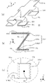
図1〜図4は、本発明の実施の形態1にかかるリード端子およびこれを用いた半導体装置について説明するためのものであって、図1は半導体装置から封止体を除いた状態を仮定したもので、図1(a)は部分平面図、図1(b)は図1(a)のB−B線による部分断面図である。図2は半導体装置に用いるリードフレームに形成されたリード端子のうちのひとつのリード端子(ソース端子)の構成を示すもので、図2(a)はリード端子の半導体素子との接合面を含む部分の斜視図、図2(b)は図2(a)の部分断面図、図2(c)は図2(a)の領域C部分の平面図である。図3は製造方法を説明するための工程に応じた半導体装置の状態を示す側面図であり、図4は製造方法を説明するためのフローチャートである。また、図5は変形例にかかるリード端子の構成を説明するためのもので、変形例ごとのリード端子の主導電部から接合面部にかけての連結部を含む部分の側面図、あるいは側面図と接合面部側から見た透過図の組み合わせである。
1 to 4 are diagrams for explaining a lead terminal according to a first embodiment of the present invention and a semiconductor device using the lead terminal, and FIG. 1 assumes a state in which a sealing body is removed from the semiconductor device. FIG. 1A is a partial plan view, and FIG. 1B is a partial cross-sectional view taken along line BB in FIG. 1A. FIG. 2 shows a configuration of one lead terminal (source terminal) of lead terminals formed on a lead frame used in a semiconductor device. FIG. 2A includes a bonding surface of the lead terminal with a semiconductor element. FIG. 2B is a partial sectional view of FIG. 2A, and FIG. 2C is a plan view of a region C portion of FIG. 2A. FIG. 3 is a side view showing the state of the semiconductor device in accordance with the steps for explaining the manufacturing method, and FIG. 4 is a flowchart for explaining the manufacturing method. FIG. 5 is a view for explaining the configuration of the lead terminal according to the modification, and is a side view of the portion including the connecting portion from the main conductive portion to the joint surface portion of the lead terminal for each modification, or joined to the side view. It is the combination of the permeation | transmission figure seen from the surface part side.
本発明の実施の形態1にかかるリード端子は、基板に配置された複数の半導体素子の表面電極に対する接合面のそれぞれが、加えられた圧力に応じて、主導電部に対して平行移動するものである。そして、半導体装置は上記構造のリード端子を用いることで、複数の半導体素子の表面電極に一括してリード端子を接合したものである。以下、図を用いて説明する。 In the lead terminal according to the first exemplary embodiment of the present invention, each of the bonding surfaces of the plurality of semiconductor elements arranged on the substrate with respect to the surface electrode is translated with respect to the main conductive portion in accordance with the applied pressure. It is. The semiconductor device uses the lead terminals having the above-described structure, and the lead terminals are collectively bonded to the surface electrodes of the plurality of semiconductor elements. This will be described below with reference to the drawings.
半導体装置1は、図1に示すように、基板4の主面上に複数の縦型半導体素子2、3が搭載されるとともに、各半導体素子が圧力に応じて接合面P51が平行移動するリード端子51により電気接続されたものである。本実施の形態1および以降の実施の形態においては、複数の縦型半導体素子2、3として、2個のスイッチング素子(MOSFET)2と2個の整流素子(SBD:Schottky diode)3を用いて2×2配列した例について説明する。2個のスイッチング素子2のそれぞれ裏面に設けたドレイン電極2dと、2個の整流素子3のそれぞれ裏面に設けたカソード電極3cとが、基板4に焼結性接合材料を用いた焼結接合部8を介して接合(電気接続)されている。そして、スイッチング素子2の表面に設けたソース電極2sおよび整流素子3の表面に設けたアノード電極3aは、それぞれ、リードフレーム5に形成されたリード端子のうち、平坦状の主導電部51mに可撓性の連結部51fを介して接合面部51jが連結されたソース端子51に接合されている。
As shown in FIG. 1, the
このとき、ソース電極2sおよびアノード電極3aと接合面P51とを焼結接合部8によって直接接合してもよいが、後述するように接合性の向上のために、本実施の形態においては、導電性金属板(導電板)7を間に入れて接合するようにしている。つまり、ソース電極2sと導電板7とを焼結接合部8を介して接合するとともに、導電板7と接合面P51とを焼結接合部8を介して接合することにより、ソース電極2sとソース端子51とを電気接続している。同様に、アノード電極3aと導電板7とを焼結接合部8を介して接合するとともに、導電板7と接合面P51とを焼結接合部8を介して接合することにより、アノード電極3aとソース端子51とを電気接続している。
At this time, the
なお、上記電気接続においては、基本的に同じ焼結性接合材料を用いて焼結接合部8を構成したが、後述する製造方法において区別するため、基板4と半導体素子2、3の裏面電極との接合部を8a、半導体素子2、3の表面電極と導電板7との接合部を8b、導電板7とソース端子51の接合面P51との接合部を8cと称して区別する。
In the electrical connection, the sintered joint 8 is basically formed using the same sinterable joining material. However, in order to distinguish in the manufacturing method described later, the back electrodes of the
スイッチング素子2のゲート電極2gは、リードフレーム5に形成された制御端子53とボンディングワイヤ6により接続されている。また、リードフレーム5に形成されたドレイン端子52は、基板4と超音波接合技術により接続されている。そして、基板4の半導体素子2、3が接合された面の反対側に形成された放熱面を除き、全体が封止樹脂9によって封止されている。
A
半導体素子2、3を構成する材料としては、シリコンウエハを基材とした一般的な素子材料でも良いが、本発明においては炭化ケイ素(SiC)や窒化ガリウム(GaN)、またはダイヤモンドといったシリコンと較べてバンドギャップが広い、いわゆるワイドバンドギャップ半導体材料を用いたときの効果が高く、特に顕著な効果が期待できる炭化ケイ素を用いた。
The material constituting the
焼結接合部8を形成する焼結性接合材料は、ナノメーターレベルの金属微粒子(金属ナノ粒子)の反応性により、その金属がバルクで示す融点よりも低い温度で焼結する現象を利用したものである。しかし、金属ナノ粒子は、その反応性の高さから、常温でも接触するだけで焼結が進行する。そのため、焼結性接合材料では、金属ナノ粒子が凝集して焼結反応が進行するのを抑制するため、金属ナノ粒子間を独立した状態で分散保持するための有機分散材によって保持されている。さらに、接合工程において焼結反応を生じさせるため、加熱により有機分散材と反応して金属ナノ粒子を裸にする分散材捕捉材と、分散材と分散材捕捉材との反応物質を捕捉して揮散する揮発性有機成分等が添加されている。つまり、焼結性接合材料は、骨材たる金属ナノ粒子が有機成分中に分散されてペースト状になったもの(ペースト8Pと称する)であり、ペースト8Pを所望の被接合部材間に供給し、加熱することで焼結接合を達成するものである。
The sinterable bonding material for forming the sintered joint 8 utilizes the phenomenon that the metal sinters at a temperature lower than the melting point shown in bulk due to the reactivity of the nanometer level metal fine particles (metal nanoparticles). Is. However, due to the high reactivity of metal nanoparticles, sintering proceeds just by contacting them at room temperature. Therefore, in the sinterable bonding material, in order to prevent the metal nanoparticles from aggregating and advancing the sintering reaction, the metal nanoparticles are held by the organic dispersion material for dispersing and holding the metal nanoparticles in an independent state. . Further, in order to cause a sintering reaction in the joining process, the dispersion trapping material that reacts with the organic dispersion material by heating to bare the metal nanoparticles, and the reactants of the dispersion material and the dispersion material trapping material are captured. Volatile organic components that volatilize are added. That is, the sinterable bonding material is a paste in which metal nanoparticles as an aggregate are dispersed in an organic component (referred to as
このとき、ペースト8P中の有機成分の分解とナノ粒子の焼結によって、接合後の焼結接合部8の体積は、初期のペースト時の体積に対して約半分程度に減少する。そのため、ボイドの少ない信頼性の高い焼結接合部8を得るためには、接合時に所定の圧を印加しながら加熱しなければならない。したがって、大電流に対応するため、ワイヤなどと比較して板厚の厚い(断面積の大きな)リードフレーム5のような配線材料を複数の半導体素子に同時に接合する場合に、素子による高さばらつきを補償して加圧できるようにする必要がある。そこで、本実施の形態に示すように、圧力に応じて接合面P51を主導電部51m側に平行移動できるように接合面部51jを主導電部51mに連結する可撓性の連結部51fで連結したリード端子構造が必要となる。
At this time, due to the decomposition of the organic component in the
ソース端子51の主導電部51mから接合面部51jにかけての構成、つまり連結部51fの構成について図2を用いて説明する。ソース端子51には、2×2配列した半導体素子2、3の電極2s、3a(厳密には導電板7を介して)とそれぞれ電気接続するための接合面P51を有する接合面部51jが設けられている。ソース端子51はリードフレーム5内に形成された端子であって、主導電部51mから接合面部51jにかけての部分も連続する板材を折り曲げることによって形成したものである。主導電部51mは、他端側が図示しない外部端子に向かって延在(x方向)し、複数の半導体素子2、3の直近上に延びる一端側が平坦状をなしており、半導体装置において基板4と平行に配置されるものである。そして、主導電部51mの一端部と中間部から幅方向に(y方向)に分岐して延びた板材のそれぞれをx軸に沿って互い違いに2回折り曲げることで、可撓性を有する連結部51fと、接合面部51jが順次形成されることになる。これにより、x方向から見たとき(図2(b))に主導電部51mから接合面部51jにかけてZ型形状をなし、主導電部51mに対して接合面P51が平行に配置される。
The configuration of the source terminal 51 from the main
ここで、接合信頼性を損なう原因である複数の半導体素子の高さのばらつきは、スイッチング素子2やダイオード3のように、もともと厚みの異なる素子を混載した場合の他、素子の製造公差によって生じる可能性があるとともに、基板4との接合部の厚みのばらつき等から生じる可能性もある。ここでは例として50μmの高さばらつき(標準高さ±25μm)が生じる場合について述べる。この場合、各接合面P51と被接合材との間(接合部材)には、連結部51fのバネ定数とバネたわみ量の違いの範囲で定まった加圧力が付与されることになる。焼結接合技術や、後の実施の形態で説明する金属間化合物接合技術で求められる加圧力としてここでは10MPaを所定の接合加圧力とし、許容されるバラつき範囲を10MPa±2.5MPaとした場合の連結部51fの形状を例示することとした。
Here, the variation in the heights of the plurality of semiconductor elements, which is a cause of impairing the junction reliability, occurs due to the manufacturing tolerance of the elements in addition to the case where elements having different thicknesses are mixedly mounted, such as the switching
連結部51fは、プレス加工にてリードフレーム5を製造する際に同時に成形されており、特にプレス曲げ工程にて主導電部51mから接合面部51jにかけてZ曲げすることで屈曲状の変形部51fb1、51fb2が成形されている。ここで、リードフレーム5の板厚を0.6mm、Z型に曲げられた連結部51fの各変形部51fb1、51fb2の曲げ角度を45度とすると、解析結果からばね定数は約3000N/mmとなり、接合面積(≒接合面部51jの面積)が30mm2だとすると、連結部51fの厚み(z方向)を0.1mm縮ませることで、接合部に所定の加圧力10MPaを付与できることになる。そこから素子の基板4からの高さが標準高さ±25μmの範囲でバラつく場合においても、接合部に生じる加圧力は7.5〜12.5MPaの範囲に収まる。つまり、上記構造の連結部51fによって主導電部51mと接合面部51jとを連結することで、素子の高さばらつきが最大50μmある場合でも、所定の加圧力バラつきの範囲内で加圧接合することが可能となることがわかる。
The connecting
さらに、図2(b)、(c)に示すように、接合面P51の中心部Pcを通る接合面P51(xy面)に垂直な軸Xc(z方向)の両側に変形部51fb1、51fb2が位置するように、連結部51fを形成した。そのため、連結部51fの高さが変化する、つまり、各変形部51fb1、51fb2の曲げ角度が変化しても、接合面P51と主導電部51m間の平行度が変化せず、面内での圧力分布も一様になる。つまり、半導体素子2、3の各電極に接合面P51を対向させ、主導電部51mに平らな面を押し当てて圧力をかけることで半導体素子2、3の電極2s、3a(導電板7)との接触面に所定範囲の圧力を印加することができる。
Further, as shown in FIGS. 2B and 2C, deformed portions 51fb1 and 51fb2 are provided on both sides of the axis Xc (z direction) perpendicular to the joint surface P51 (xy plane) passing through the center portion Pc of the joint surface P51. The connecting
また、ここでは素子高さの違いが最大50μmである場合について説明したが、これ以上の厚さ範囲でバラつく可能性がある場合でも、連結部51fの板厚を薄くしたり、曲げ角度を大きくしたりすることで解決可能である。その際にも、接合面P51の中心部Pcを通る軸Xcの両側に変形部51fb1、51fb2が位置するように、連結部51fを形成すれば、必要な変形量が変化しても、接合面P51内にかかる圧力分布を一様にすることができる。
In addition, although the case where the difference in element height is 50 μm at the maximum has been described here, even when there is a possibility of variations in the thickness range beyond this, the thickness of the connecting
なお、焼結性接合材料との接合性を考慮して、接合面P51には、金(Au)、銀(Ag)、銅(Cu)などの金属膜、あるいは、金、銀、銅、白金(Pt)、パラジウム(Pd)などが最表面にくるような薄膜層が形成されている。 In consideration of the bondability with the sinterable bonding material, the bonding surface P51 has a metal film such as gold (Au), silver (Ag), copper (Cu), or gold, silver, copper, platinum. A thin film layer is formed such that (Pt), palladium (Pd), and the like are on the outermost surface.
一方、焼結性接合材料で接続される半導体素子2、3の電極2s、2d、3aおよび3cも、焼結性接合材料との接合性を考慮して、厚さ数百nm〜数μmの金、銀、銅などの電極膜で形成、あるいは、金、銀、銅、白金、パラジウムなどが最表面にくるように例えばニッケル(Ni)/金といった薄膜層構造で形成している。なお、接合面部51jや半導体素子2、3に形成する電極の材料としては、上記材料に限定されることはなく、焼結性接合材料や被接合材、および基板4、導電板7との接合性や安定性等を考慮して適宜選定すればよい。
On the other hand, the
ただし、製造プロセスの初期工程から熱履歴を受ける半導体素子2、3の電極をニッケル/金といった薄膜多層構造で形成した場合、以下のような場合には、製造プロセスについて考慮する必要がある。電極最表面の薄膜厚が例えば金メタライズで数十〜200nm程度と薄く、かつその下地層として焼結性接合材料との接合性に劣る金属(例えばニッケル)が用いられると、複数回の加熱製造プロセス中に付与される熱履歴によってニッケル下地層が電極最表面にまで拡散してくることがあり、接合性の低下を招く。その場合、後述する導電板7を用いた製造方法が接合性の低下を抑制するうえで有効になる。
However, when the electrodes of the
導電板7は、焼結性接合材料を用いた接合技術によって接合可能な接合部表面状態を有する金属板であり、接合部表面は金、銀、銅、白金、パラジウムなどが望ましい。このとき、導電板7の材質を導電性のあるアルミニウム(Al)や銅、ニッケル、チタン(Ti)、鉄(Fe)等の金属材料やCu−Mo、Al−SiCなどの導電性セラミック複合材料、Cu−Invar−Cuなどのクラッド材料とし、接合部表面にのみ焼結接合技術で接合可能な上記金属をめっき等によって設けてもかまわない。ただし、上記表面に施した接合可能な金属層は、少なくとも500nm以上、理想的には1〜5μm程度の厚さを有し、複数回の加熱プロセスに伴う熱履歴後も接合部表面に接合性に劣る金属が拡散し湧出してこないよう配慮されたものでなければならない。なお、図1では、説明を簡略化するため、スイッチング素子2の表面には、ひとつの電極2sのみに導電板7を適用している例について記載しているが、表面に複数の電極(主電力用)が区分けして形成されている場合でも適用可能である。
The
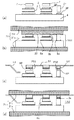
次に、上記半導体装置1を製造する方法について図3の側面図と図4のフローチャートのステップ番号を用いて説明する。なお、図3(以降の実施の形態における図7、図9も)は、側面を示すものであるが、その工程において注目すべき部材にハッチングを施して表現している。
まず、図3(a)に示すように、基板4の半導体素子2、3を接合する領域にペースト8Pを供給する(ステップS110)とともに、半導体素子2、3のソース電極2s、アノード電極3aにもペースト8Pを供給する(ステップS120)。そして、基板4のペースト8Pを供給した部分に、半導体素子2、3の裏面電極であるドレイン電極2d、カソード電極3cを合わせるように設置する。さらに、設置した半導体素子2、3のペースト8Pが供給された部分にそれぞれ導電板7を設置し(ステップS200)、1回目接合における被接合体とする。
Next, a method for manufacturing the
First, as shown in FIG. 3A, the
その後、図3(b)に示すように、被接合体を加熱プレス装置21に挿入し、加熱プレスステージ面21sと加熱プレスツール面21tとで加熱加圧して、1回目接合を行う(ステップS300)。このとき、半導体素子2、3の厚さ(基板4からの高さ)が異なる場合にも所定範囲の加圧力がかかるように、被接合体と加熱プレスツール面21tとの間には、所定のばね係数に相当するクッション性を有するシート材(緩衝部材)22を挿入する。これにより、焼結接合部8aおよび8bが形成され、基板4と半導体素子2、3の裏面電極2d、3cとの電気接続および半導体素子2、3のソース電極2s、アノード電極3aと導電板7との電気接続が達成され、1次組立体1A1が形成される。
Then, as shown in FIG.3 (b), a to-be-joined body is inserted in the
続いて、図3(c)に示すようにリードフレーム5の接合面P51にペースト8Pを供給する(ステップS130)。そして、1次組立体1A1と加熱プレスツール面21tとの間の緩衝部材22を取り外し、導電板7とペースト8Pが供給された接合面P51とを位置合わせしながらリードフレーム5を1次組立体1A1上に設置し(ステップS400)、2回目接合における被接合体とする。その後、図3(d)に示すように、再び加熱プレス装置21にて被接合体を直接加熱加圧して2回目接合を行う。これにより、焼結接合部8cが形成され、導電板7とソース端子51との電気接続が達成され2次組立体1A2が形成される。
Subsequently, as shown in FIG. 3C, the
このとき、従来のようにリード端子の主導電部(本体)と接合面との間に可撓性を有する部材が介在していない場合、たとえ1回目接合のようにクッション性のある緩衝部材22を用いたとしても、リードフレームが厚さ(高さ)の異なる半導体素子2、3に応じて変形することができないので、接合不良が発生する可能性が高い。しかしながら、本実施の形態に示すように、ソース端子51は主導電部51mと接合面部51jとを可撓性のある連結部51fで連結したので、高さが異なる素子に対しても、所定範囲の面圧をかけることができ、焼結接合技術による信頼性の高い焼結接合部8の形成が可能となり、結果、半導体装置1の耐熱性および信頼性を向上させることができる。
At this time, when a member having flexibility is not interposed between the main conductive portion (main body) of the lead terminal and the joining surface as in the conventional case, the cushioning
また、接合面P51の中心部Pcを通る軸Xcの両側に変形部51fb1、51fb2が位置するように、連結部51fを形成したので、接合面P51の面内での圧力分布も一様になるので、より信頼性の高い接合が可能となる。
Further, since the connecting
その後、ドレイン端子52を基板4に対して超音波接合したり、制御端子53とゲート電極2gとをボンディングワイヤ6でワイヤボンドしたりすることで、電気配線が完了する。さらに、基板4の半導体素子2、3が接合された面の反対側に形成された放熱面を除き、全体を封止樹脂9によって封止し、リードフレーム5の各端子を切り離し、折り曲げ形成する等をしてパッケージ化された半導体装置1が完成する。
Thereafter, the
なお、本実施の形態1においては、上述したように複数回の加熱プロセスに伴う熱履歴後に、半導体素子2、3の表面電極の表面に接合性に劣る金属が拡散し湧出してくる場合も想定して、導電板7を表面電極上に接合するようにしたものである。そのため、このような場合を想定する必要がない場合は、必ずしも導電板7を使用する必要はない。ただし、半導体素子上に導電板を予め基板と同時に接合しておくと、半導体素子表面電極とリードフレームとの位置関係を厳密に制御しなくとも、素子の電極外と接合材あるいはリードフレームとの接触を防止するという効果を得ることもできる。
In the first embodiment, as described above, after the thermal history associated with a plurality of heating processes, a metal having poor bonding properties may diffuse and spring out on the surfaces of the surface electrodes of the
実施の形態1の変形例.
一方、連結部51fを含む主導電部51mから接合面部51jにかけての形状は上記Z型構造に限るものではない。ただし、リードフレーム5を介して加圧した際に、変形部の変形に伴って、接合面P51が導電板7のような被接合面に対して跳ね上がり、平行を維持できるように連結部51fが変形するような構造でなくてはならない。そのため、接合面P51の中心Pcを通る接合面P51に垂直な軸Xcの両側に、少なくとも一対の変形部を有するような構造でなければならない。
Modification of the first embodiment.
On the other hand, the shape from the main
例えば図5(a)、図5(b)に示すようにM型、L型などが例として挙げられる。図5(a)においては、屈曲状の変形部51fb1〜51fb3のうち、51fb1と51fb3が軸Xcを挟んで変形部51fb2と対峙するように構成している。図5(b)においては、屈曲状の変形部51fb1が軸Xcを挟んで変形部51fb2と対峙するように構成している。これにより、連結部51fの高さ(主導電部51m〜接合面P51間の厚み)が変化しても、接合面P51は主導電部51mに対しての平行を維持する、つまり被接合面である半導体素子2、3の電極面との平行を維持することが可能となり、面内で面圧を一様に保つことができる。
For example, as shown in FIG. 5 (a) and FIG. 5 (b), examples include M type and L type. In FIG. 5A, among the bent deformation portions 51fb1 to 51fb3, 51fb1 and 51fb3 are configured to face the deformation portion 51fb2 across the axis Xc. In FIG. 5B, the bent deformable portion 51fb1 is configured to face the deformable portion 51fb2 across the axis Xc. As a result, even if the height of the connecting
また、上記変形例も含め、本実施の形態ではリードフレーム5を製造するプレス工程にて連結部51fを設ける(形成する)としたが、別途連結部や接合面部となる部材を作製し、リードフレームに別途作製した連結部や接合面部を溶接、ろう付け、超音波接合、圧接などの導電性を確保できる接合技術で接合してあっても良い。接合面部の材質は少なくとも最表面が焼結性金属材料等の接合部材との接合性及び導電性があるものであればよく、連結部の材質は導電性を示す金属材料であれば特に制限はなく、形状もより自由度が高くなる。例えば、図5(c1)、(c2)に示すようにコイルバネ状の連結部51fとすれば、中心Pcを通る軸Xcを囲むようにらせん状の変形部51fbvが形成されているので、軸Xcを挟んで少なくとも対となる変形部を有することになる。
In addition, in the present embodiment, including the above-described modification, the connecting
また例えば、図5(d1)、(d2)に示すようにポーラス金属状(多孔金属)の柱状物とすれば、多孔金属を形成する粒子同士の結合部分が変形部となり、柱状物の体積内に変形部が分布することになる。つまり、中心Pcを通る軸Xcを囲むように変形部51fbpが形成されていることになるので、軸Xcを挟んで少なくとも対となる変形部を有することになる。
Further, for example, as shown in FIGS. 5 (d1) and 5 (d2), if a porous metal-like (porous metal) columnar material is used, the bonded portion between the particles forming the porous metal becomes a deformed portion, and the volume of the columnar material is within the range. Therefore, the deformed parts are distributed. That is, since the deformed portion 51fbp is formed so as to surround the axis Xc passing through the center Pc, the
以上のように、本発明の実施の形態1にかかるリード端子であるソース端子51あるいはソース端子51を有するリードフレーム5によれば、基板4の主面に複数の半導体素子2、3が配置された半導体装置1に用いられ、複数の半導体素子2、3のそれぞれの表側の電極2s、3aと外部回路とを電気接続するためのリード端子51であって、基板4の主面に対して略平行に配置される平坦状の主導電部51mと、主導電部51mに対して面の垂直方向(z)に所定の間隔をあけるとともに、面の延在方向(xy)の所定位置にそれぞれ形成され、複数の半導体素子2、3のそれぞれの表側の電極2s、3aに対向するように配置される接合面P51を有する接合面部51jと、主導電部51mとそれぞれの接合面P51間に加えた圧力に応じて、それぞれの接合面P51と主導電部51mとの平行を維持しながら、当該接合面P51と主導電部51j間の間隔が変化するように接合面部51jのそれぞれと主導電部51mとを連結する連結部51fと、を備えるように構成した。そのため、ソース端子51の各接合面P51と複数の半導体素子2、3とを一括して接合する場合、各素子の高さにばらつきがあっても、加えた力に応じて、接合面P51と電極2s、3aとの平行を保ったまま、高さを変化させることができるので、平らな面で挟んで所定の圧を加えれば、各素子に対して適切な圧力範囲の圧力をかけて接合することができる。そのため、耐熱性の高い焼結性接合技術を用いても、効率よく製造できるとともに、信頼性が高い接合が可能となる。
As described above, according to the
とくに、連結部51fのそれぞれには、当該連結部51fが連結する接合面部51jの接合面P51の中心Pcを通る接合面P51に垂直な軸Xcを挟むように、圧力に応じて変形する変形部51fbが形成されているように構成した。そのため、主導電部51mと接合面P51間に力を加えた場合、接合面P51と主導電部51mに対する平行度を維持して変形することが可能となり、接合面P51と被接合体との圧力分布を確実に一様に保つことができる。
In particular, each of the connecting
また、連結部51fから接合面部51jにかけての部分は、それぞれ主導電部51mから延在する板材を折り曲げて形成するようにしたので、容易にリード端子を形成することができる。
Further, since the portion from the connecting
あるいは、変形例に示すように、連結部51fから接合面部51jにかけての部分は、それぞれ可撓性部材(例えばコイルや多孔金属材)と板材とを主導電部51mの面内の所定位置に接合して形成するようにすれば、圧力範囲の制御や面圧の一様性等をより容易にコントロールできる。
Alternatively, as shown in the modified example, the portion from the connecting
可撓性部材として、軸Xcを囲むように旋回するコイル材にすれば、圧力範囲の制御や面圧の一様性等を容易にコントロールできる。 If the coil member is turned so as to surround the axis Xc as the flexible member, the control of the pressure range, the uniformity of the surface pressure, and the like can be easily controlled.
また、可撓性部材として、多孔金属からなる柱状材を用いても圧力範囲の制御や面圧の一様性等を容易にコントロールできる。 Further, even when a columnar material made of porous metal is used as the flexible member, the control of the pressure range, the uniformity of the surface pressure, and the like can be easily controlled.
また、本発明の実施の形態1にかかる半導体装置1によれば、基板4と、基板4の主面に裏側の電極2d、3cが接合された複数の半導体素子2、3と、複数の半導体素子2、3のそれぞれの表側の電極2s、3aに接合面P51が接合された上述したリード端子であるソース端子51あるいはソース端子51が形成されたリードフレーム5と、を備えるように構成した。そのため、ソース端子51の各接合面P51と複数の半導体素子2、3とを一括して接合する場合、各素子の高さにばらつきがあっても、加えた力に応じて、接合面P51の高さが平行移動するので、平らな面で挟んで所定の圧を加えれば、各素子に対して適切な圧力範囲の圧力をかけて接合することができる。そのため、耐熱性の高い焼結性接合技術を用いても、効率よく製造できるとともに、接合信頼性が高く、劣化が少なく長寿命となる。
Further, according to the
とくに、表側の電極2s、3a(あるいはそれに接合した導電板7)と接合面P51との接合が焼結接合技術により行われたので、接合信頼性が高く、高温動作を繰り返しても劣化が少なく長寿命となる。
In particular, since the
実施の形態2.
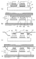
本実施の形態2にかかる半導体装置では、実施の形態1と異なり、ドレイン端子にも可撓性の連結部を設け、焼結性接合材を用い、導電ブロックを介して基板とドレイン端子とを接合するようにしたものである。その他の構成については実施の形態1と同様である。図6〜図8は、本発明の実施の形態2にかかる半導体装置について説明するためのものであって、図6は半導体装置から封止体を除いた状態を仮定したもので、図6(a)は部分平面図、図6(b)は図6(a)のB2−B2線による部分断面図である。図7は製造方法を説明するための工程に応じた半導体装置の状態を示す側面図であり、図8は製造方法を説明するためのフローチャートである。
In the semiconductor device according to the second embodiment, unlike the first embodiment, the drain terminal is provided with a flexible connecting portion, a sinterable bonding material is used, and the substrate and the drain terminal are connected via the conductive block. It is made to join. Other configurations are the same as those in the first embodiment. 6 to 8 are for explaining the semiconductor device according to the second embodiment of the present invention, and FIG. 6 assumes a state in which the sealing body is removed from the semiconductor device, and FIG. FIG. 6A is a partial plan view, and FIG. 6B is a partial cross-sectional view taken along line B2-B2 of FIG. FIG. 7 is a side view showing the state of the semiconductor device in accordance with the steps for explaining the manufacturing method, and FIG. 8 is a flowchart for explaining the manufacturing method.
図6に示すように、本実施の形態2にかかる半導体装置1においては、ドレイン端子52にも、主導電部52mと接合面部52jとを可撓性を有する連結部52fで連結するように形成されている。そして、接合面部52jの接合面P52と基板4とは、半導体素子2、3の厚み(本実施の形態では半導体素子の裏面電極から導電板7までの厚み)に相当する厚みを有する導電ブロック27を介して焼結接合部8を用いて電気接続されている。連結部52fの形状は、実施の形態1と同様の条件を満たすものとしてZ型とした。
As shown in FIG. 6, in the
なお、上記電気接続においても、実施の形態1と同様に基本的に同じ焼結性接合材料を用いて焼結接合部8を構成したが、後述する製造方法において区別するため、基板4と導電ブロック27との接合部を8d、導電ブロック27とドレイン端子52の接合面P52との接合部を8eと称して区別する。
In the electrical connection as well, the sintered joint 8 is basically formed using the same sinterable joining material as in the first embodiment. However, in order to distinguish in the manufacturing method described later, the
導電ブロック27は、焼結性接合材料を用いた接合技術によって接合可能な接合部表面状態を有する導電性ブロックであり、接合部表面は金、銀、銅であることが望ましい。このとき、導電ブロック27材質を導電性のあるアルミニウムや銅、ニッケル、チタン、鉄等の金属材料やCu−Mo、Al−SiCなどの導電性セラミック複合材料、Cu−Invar−Cuなどのクラッド材料とし、接合部表面にのみ焼結接合技術で接合可能な上記金属をめっき等によって設けてもかまわない。
The
次に、上記半導体装置1を製造する方法について図7の側面図と図8のフローチャートのステップ番号を用いて説明する。
まず、図7(a)に示すように、基板4の半導体素子2、3および導電ブロック27を接合する領域にペースト8Pを供給する(ステップS112)とともに、半導体素子2、3のソース電極2s、アノード電極3aにもペースト8Pを供給する(ステップS120)。そして、基板4のペースト8Pを供給した部分に、半導体素子2、3の裏面電極であるドレイン電極2d、カソード電極3c、および導電ブロック27を合わせるように設置する。さらに、設置した半導体素子2、3のペースト8Pが供給された部分にそれぞれ導電板7を設置し(ステップS202)、1回目接合における被接合体とする。
Next, a method for manufacturing the
First, as shown in FIG. 7A, a
その後、図7(b)に示すように、被接合体を加熱プレス装置21に挿入し、加熱プレスステージ面21sと加熱プレスツール面21tとで加熱加圧して、1回目接合を行う(ステップS300)。このとき、半導体素子2、3、および導電ブロック27の厚さ(基板4からの高さ)が異なる場合にも所定範囲の加圧力がかかるように、被接合体と加熱プレスツール面21tとの間には、クッション性のあるシート材(緩衝部材)22を挿入する。これにより、焼結接合部8a、8bおよび8dが形成され、基板4と半導体素子2、3の裏面電極2d、3cとの電気接続、半導体素子2、3のソース電極2s、アノード電極3aと導電板7との電気接続、および基板4と導電ブロック27との電気接続が達成され、1次組立体1A1が形成される。
Then, as shown in FIG.7 (b), a to-be-joined body is inserted in the
続いて、図7(c)に示すようにリードフレーム5の接合面P51、P52にペースト8Pを供給する(ステップS132)。そして、1次組立体1A1と加熱プレスツール面21tとの間の緩衝部材22を取り外し、導電板7とペースト8Pが供給された接合面P51と、および導電ブロック27とペースト8Pが供給された接合面P52とを位置合わせしながらリードフレーム5を1次組立体1A1上に設置し(ステップS402)、2回目接合における被接合体とする。その後、図7(d)に示すように、再び加熱プレス装置21にて被接合体を直接加熱加圧して2回目接合を行う。これにより、焼結接合部8c、8eが形成され、導電板7とソース端子51との電気接続、および導電ブロック27とドレイン端子52との電気接続が達成され2次組立体1A2が形成される。
Subsequently, as shown in FIG. 7C, the
以上のように、本実施の形態2にかかる半導体装置1によれば、リードフレーム5に形成されたリード端子のうち、基板4と電気接合するためのドレイン端子52にも、接合面部52jと主導電部52mとを可撓性のある連結部52fで連結するように構成し。接合面P52と基板4とを半導体素子2、3の厚みに相当する導電ブロック7を介して接合するようにしたので、ドレイン端子52も半導体素子2、3と同時に接合できるとともに、適切な面圧範囲に制御でき、信頼性の高い接合が可能となる。とくに、ドレイン端子52と基板4との超音波接合による接続工程を省略でき、生産性を向上させる効果がある。
As described above, according to the
実施の形態3.
本実施の形態3にかかる半導体装置は、実施の形態1および2で用いた焼結性接合技術の代わりに金属間化合物接合技術(例えば、特許文献4参照。)を用いたものである。金属間化合物接合技術とは、錫(Sn)と銀との金属間化合物(Ag3Sn)層、または錫と銅との金属間化合物(Cu3Sn)層を形成することで接合するものであり、被接合面の少なくとも一方が銀または銅である必要があり、ともに銀、またはともに銅であることが望ましい。そして、被接合面の少なくとも一方に銀または銅と反応させるための錫層を形成しておく必要がある。それ以外の構成については、基本的に、実施の形態2で説明したものと同様であり、同様部分については説明を省略する。
The semiconductor device according to the third embodiment uses an intermetallic compound bonding technique (see, for example, Patent Document 4) instead of the sinterable bonding technique used in the first and second embodiments. Intermetallic compound joining technology is a technique for joining by forming an intermetallic compound (Ag 3 Sn) layer of tin (Sn) and silver or an intermetallic compound (Cu 3 Sn) layer of tin and copper. Yes, at least one of the surfaces to be joined must be silver or copper, and it is desirable that both are silver or copper. And it is necessary to form the tin layer for making it react with silver or copper in at least one of a to-be-joined surface. Other configurations are basically the same as those described in the second embodiment, and the description of the same parts is omitted.
なお、接合層(接合部)の形成メカニズムについてはここでは省略するが、金属間化合物接合技術によって接合を行うためには、被接合面への適切な金属膜構造の形成および、適正な圧力をかけた状態で加熱処理する必要がある。そのため、金属間化合物接合技術を用いる場合でも上述したように、可撓性のある連結部で接合面部が連結されたリード端子を用いることが有効となる。あるいは、金属間化合物接合技術で形成する接合部自体の厚みは、基本的にペーストを塗布して形成した焼結接合部よりも薄くなるので、可撓性のある連結部で接合面部が連結されたリード端子を用いたときの接合信頼性の向上効果はさらに顕著になる。 Although the formation mechanism of the bonding layer (bonding portion) is omitted here, in order to perform bonding by the intermetallic compound bonding technique, an appropriate metal film structure is formed on the bonded surface and an appropriate pressure is applied. It is necessary to heat-treat in the applied state. Therefore, even when using an intermetallic compound bonding technique, as described above, it is effective to use a lead terminal in which the bonding surface portion is connected by a flexible connecting portion. Alternatively, since the thickness of the joint itself formed by the intermetallic compound joining technique is basically thinner than the sintered joint formed by applying the paste, the joint surface portion is connected by a flexible connecting portion. The effect of improving the bonding reliability when using the lead terminals becomes even more remarkable.
次に、上記半導体装置を製造する方法について、図に基づいて説明する。図9と図10は、本発明の実施の形態3にかかる半導体装置について説明するためのものであって、図9は製造方法を説明するための工程に応じた半導体装置の状態を示す側面図であり、図10は製造方法を説明するためのフローチャートである。なお、基板4、リードフレーム5、導電板7および導電ブロック27の材料として、銅を用いた場合について説明する。
Next, a method for manufacturing the semiconductor device will be described with reference to the drawings. FIG. 9 and FIG. 10 are for explaining the semiconductor device according to the third embodiment of the present invention, and FIG. 9 is a side view showing the state of the semiconductor device in accordance with the steps for explaining the manufacturing method. FIG. 10 is a flowchart for explaining the manufacturing method. The case where copper is used as the material of the
まず、図9(a)に示すように、半導体素子2、3の主電力を流す表裏の電極(ソース電極2s、ドレイン電極2d、アノード電極3a、カソード電極3c)上に、銅の金属層81を形成し、銅の金属層81上にさらに錫層82を形成する(ステップS123)。さらに、銅の導電ブロック27の基板4との接合面に錫層82を形成する(ステップS143)。そして、基板4の所定位置に、半導体素子2、3の裏面電極であるドレイン電極2d、カソード電極3c、および導電ブロック27を合わせて設置する。さらに、設置した半導体素子2、3のソース電極2sとアノード電極2a上にそれぞれ導電板7を設置し(ステップS203)、1回目接合における被接合体とする。
First, as shown in FIG. 9A, a
その後、図9(b)に示すように、被接合体を加熱プレス装置21に挿入し、加熱プレスステージ面21sと加熱プレスツール面21tとで加熱加圧して、1回目接合を行う(ステップS303)。このとき、半導体素子2、3、および導電ブロック27の厚さ(基板4からの高さ)が異なる場合にも所定範囲の加圧力がかかるように、被接合体と加熱プレスツール面21tとの間には、クッション性のあるシート材(緩衝部材)22を挿入する。これにより、金属間化合物接合層(部)83a、83bおよび83dが形成され、基板4と半導体素子2、3の裏面電極2d、3cとの電気接続、半導体素子2、3のソース電極2s、アノード電極3aと導電板7との電気接続、および基板4と導電ブロック27との電気接続が達成され、1次組立体1A1が形成される。
Thereafter, as shown in FIG. 9B, the object to be joined is inserted into the
続いて、図9(c)に示すようにリードフレーム5の接合面P51、P52に錫層82を形成する(ステップS133)。そして、1次組立体1A1と加熱プレスツール面21tとの間の緩衝部材22を取り外し、導電板7と錫層82が形成された接合面P51と、および導電ブロック27と錫層82が形成された接合面P52とを位置合わせしながらリードフレーム5を1次組立体1A1上に設置し(ステップS403)、2回目接合における被接合体とする。その後、図9(d)に示すように、再び加熱プレス装置21にて被接合体を直接加熱加圧して2回目接合を行う。これにより、金属間化合物接合層(部)83c、83eが形成され、導電板7とソース端子51との電気接続、および導電ブロック27とドレイン端子52との電気接続が達成され2次組立体1A2が形成される。
Subsequently, as shown in FIG. 9C, a
上記工程において、金属層81、基板4、導電板7、導電ブロック27、ソース端子51およびドレイン端子52の材料として銅をベースとした場合について説明したが、被接合面の最表面に銅がくるようにめっき等により薄膜を設けたものでもよい。その場合金属間化合物接合層はCu3Sn相から形成される。また、材料として銀をベースとした場合、あるいは被接合面の最表面に銀がくるようにめっき等により薄膜が設けたもので上記工程を行った場合、金属間化合物接合層はAg3Sn相から形成される。
In the above process, the case where copper is used as the material for the
以上のように、本実施の形態3にかかる半導体装置1によれば、主導電部52mと可撓性のある連結部51fで連結された接合面部51jの接合面P51と表側の電極2s、3aとの接合が金属間化合物接合技術により行われるようにした。そのため、ソース端子51の各接合面P51と複数の半導体素子2、3とを一括して接合する場合、各素子の高さにばらつきがあっても、加えた力に応じて、接合面P51の高さが平行移動するので、平らな面で挟んで所定の圧を加えれば、各素子に対して適切な圧力範囲の圧力をかけて接合することができる。そのため、耐熱性の高い金属間化合物接合技術を用いても、効率よく製造できるとともに、接合信頼性が高く、劣化が少なく長寿命となる。
As described above, according to the
なお、上記各実施の形態1〜3では、半導体素子2、3(あるいは導電板7)と接合面P51との接合を高耐熱技術である焼結性接合材料による焼結接合部8や金属間化合物接合材料による金属間化合物接合部83を例に説明したが、これに限定する必要はない。例えば、はんだやろう材といったその他の材料であっても、接合面に均一な面圧を印加できるリード端子51や52を用いることで、信頼性の高い接合が可能となる。ただし、上述した焼結接合技術や金属間化合物接合技術のように、接合時の面圧条件が厳しい接合技術ほど、より本発明による効果を発揮することができる。
In each of the first to third embodiments, the bonding between the
また、上記各実施の形態においては、半導体素子には、炭化ケイ素によって形成されたものを示したが、これに限られることはなく、一般的に用いられているケイ素(Si)で形成されたものであってもよい。しかし、ケイ素よりもバンドギャップが大きい、いわゆるワイドギャップ半導体を形成できる炭化ケイ素や、窒化ガリウム系材料又はダイヤモンドを用いた時の方が、動作温度が高く、より、耐熱性の高い接合技術が求められるため、本発明による効果をより一層発揮することができる。 In each of the above embodiments, the semiconductor element is formed of silicon carbide. However, the semiconductor element is not limited to this, and is formed of silicon (Si) that is generally used. It may be a thing. However, the use of silicon carbide that can form so-called wide gap semiconductors, gallium nitride-based materials, or diamond, which has a larger band gap than silicon, requires a higher operating temperature and higher heat resistance bonding technology. Therefore, the effect by this invention can be exhibited further.
1 半導体装置、
2 スイッチング素子(MOSFET)、 2d ドレイン電極(裏面電極)、 2g
ゲート電極(表面電極)、 2s ソース電極(表面電極)、
3 整流素子(SBD)、 3a アノード電極(表面電極)、 3c カソード電極(裏面電極)、
4 基板、
5 リードフレーム、 51 ソース端子(51f:連結部、51fb:変形部、51j:接合面部)、 51m 主導電部、 52 ドレイン端子(52f:連結部、52j:接合面部、52m:主導電部)、 53 制御端子、
6 ボンディングワイヤ、 7 導電性金属板(導電板)、
8 焼結接合部(接合部)、 83 金属間化合物接合部(接合部)、
9 封止樹脂(封止体)、 21 加熱プレス装置、 22 緩衝材、
P51,P52 接合面、 Pc 接合面の中心、 Xc 接合面の中心を通る接合面に垂直な軸。
1 Semiconductor device,
2 switching element (MOSFET), 2d drain electrode (back electrode), 2g
Gate electrode (surface electrode), 2s source electrode (surface electrode),
3 rectifying element (SBD), 3a anode electrode (front surface electrode), 3c cathode electrode (back surface electrode),
4 substrates,
5 lead frame, 51 source terminal (51f: connecting portion, 51fb: deformed portion, 51j: joint surface portion), 51m main conductive portion, 52 drain terminal (52f: connecting portion, 52j: joint surface portion, 52m: main conductive portion), 53 control terminal,
6 Bonding wire, 7 Conductive metal plate (conductive plate),
8 Sintered joint (joint), 83 Intermetallic compound joint (joint),
9 sealing resin (sealing body), 21 heating press device, 22 cushioning material,
P51, P52 joint surface, center of the Pc joint surface, and axis perpendicular to the joint surface passing through the center of the Xc joint surface.
Claims (11)
平坦状の主導電部と、
前記主導電部に対して面の垂直方向に所定の間隔をあけるとともに、面の延在方向の所定位置にそれぞれ形成され、前記複数の半導体素子のそれぞれの表側の電極に対向するように配置される接合面を有する接合面部と、
前記主導電部とそれぞれの接合面間に加えた圧力に応じて、当該接合面と前記主導電部との平行を維持しながら、当該接合面と前記主導電部間の間隔が変化するように前記接合面部のそれぞれと前記主導電部とを連結する連結部と、
を備えたことを特徴とするリード端子。 A lead terminal for use in a semiconductor device in which a plurality of semiconductor elements are arranged on a main surface of a substrate, and for electrically connecting each front-side electrode of the plurality of semiconductor elements and an external circuit,
A flat main conductive portion;
The main conductive portion is spaced apart in a direction perpendicular to the surface, is formed at a predetermined position in the surface extending direction, and is disposed so as to face each front side electrode of the plurality of semiconductor elements. A bonding surface portion having a bonding surface;
In accordance with the pressure applied between the main conductive portion and each joint surface, the interval between the joint surface and the main conductive portion is changed while maintaining the parallelness between the joint surface and the main conductive portion. A connecting portion that connects each of the joint surface portions and the main conductive portion;
A lead terminal comprising:
前記基板の主面に裏側の電極が接合された複数の半導体素子と、
前記複数の半導体素子のそれぞれの表側の電極に前記接合面が接合された請求項1ないし6のいずれか1項に記載のリード端子と、
を備えたことを特徴とする半導体装置。 A substrate,
A plurality of semiconductor elements in which electrodes on the back side are bonded to the main surface of the substrate;
The lead terminal according to any one of claims 1 to 6, wherein the bonding surface is bonded to an electrode on a front side of each of the plurality of semiconductor elements.
A semiconductor device comprising:
Priority Applications (1)
| Application Number | Priority Date | Filing Date | Title |
|---|---|---|---|
| JP2011279295A JP2013131592A (en) | 2011-12-21 | 2011-12-21 | Lead terminal and semiconductor device using the same |
Applications Claiming Priority (1)
| Application Number | Priority Date | Filing Date | Title |
|---|---|---|---|
| JP2011279295A JP2013131592A (en) | 2011-12-21 | 2011-12-21 | Lead terminal and semiconductor device using the same |
Publications (2)
| Publication Number | Publication Date |
|---|---|
| JP2013131592A true JP2013131592A (en) | 2013-07-04 |
| JP2013131592A5 JP2013131592A5 (en) | 2014-01-09 |
Family
ID=48908934
Family Applications (1)
| Application Number | Title | Priority Date | Filing Date |
|---|---|---|---|
| JP2011279295A Pending JP2013131592A (en) | 2011-12-21 | 2011-12-21 | Lead terminal and semiconductor device using the same |
Country Status (1)
| Country | Link |
|---|---|
| JP (1) | JP2013131592A (en) |
Cited By (6)
| Publication number | Priority date | Publication date | Assignee | Title |
|---|---|---|---|---|
| JP2015153966A (en) * | 2014-02-18 | 2015-08-24 | 三菱電機株式会社 | Semiconductor device and semiconductor device manufacturing method |
| JPWO2016159070A1 (en) * | 2015-04-03 | 2017-06-22 | 三菱電機株式会社 | Semiconductor element bonding method and sheet-shaped laminated cushioning material for semiconductor element bonding |
| JP2019071448A (en) * | 2014-10-21 | 2019-05-09 | オスラム オプト セミコンダクターズ ゲゼルシャフト ミット ベシュレンクテル ハフツングOsram Opto Semiconductors GmbH | Electronic device and manufacturing method thereof |
| CN112041972A (en) * | 2018-04-27 | 2020-12-04 | 日东电工株式会社 | Method for manufacturing semiconductor device |
| DE102022124463A1 (en) | 2021-11-16 | 2023-05-17 | Mitsubishi Electric Corporation | semiconductor device |
| WO2023190180A1 (en) * | 2022-03-30 | 2023-10-05 | ローム株式会社 | Semiconductor device |
Citations (3)
| Publication number | Priority date | Publication date | Assignee | Title |
|---|---|---|---|---|
| JPH0742967U (en) * | 1993-12-28 | 1995-08-11 | 新電元工業株式会社 | Resin-sealed semiconductor device |
| JP2008227131A (en) * | 2007-03-13 | 2008-09-25 | Renesas Technology Corp | Semiconductor device and its manufacturing method |
| JP2013135105A (en) * | 2011-12-27 | 2013-07-08 | Mitsubishi Electric Corp | Power semiconductor device |
-
2011
- 2011-12-21 JP JP2011279295A patent/JP2013131592A/en active Pending
Patent Citations (3)
| Publication number | Priority date | Publication date | Assignee | Title |
|---|---|---|---|---|
| JPH0742967U (en) * | 1993-12-28 | 1995-08-11 | 新電元工業株式会社 | Resin-sealed semiconductor device |
| JP2008227131A (en) * | 2007-03-13 | 2008-09-25 | Renesas Technology Corp | Semiconductor device and its manufacturing method |
| JP2013135105A (en) * | 2011-12-27 | 2013-07-08 | Mitsubishi Electric Corp | Power semiconductor device |
Cited By (8)
| Publication number | Priority date | Publication date | Assignee | Title |
|---|---|---|---|---|
| JP2015153966A (en) * | 2014-02-18 | 2015-08-24 | 三菱電機株式会社 | Semiconductor device and semiconductor device manufacturing method |
| JP2019071448A (en) * | 2014-10-21 | 2019-05-09 | オスラム オプト セミコンダクターズ ゲゼルシャフト ミット ベシュレンクテル ハフツングOsram Opto Semiconductors GmbH | Electronic device and manufacturing method thereof |
| JPWO2016159070A1 (en) * | 2015-04-03 | 2017-06-22 | 三菱電機株式会社 | Semiconductor element bonding method and sheet-shaped laminated cushioning material for semiconductor element bonding |
| CN112041972A (en) * | 2018-04-27 | 2020-12-04 | 日东电工株式会社 | Method for manufacturing semiconductor device |
| EP3787011A4 (en) * | 2018-04-27 | 2022-06-08 | Nitto Denko Corporation | Semiconductor device manufacturing method |
| US11594513B2 (en) | 2018-04-27 | 2023-02-28 | Nitto Denko Corporation | Manufacturing method for semiconductor device |
| DE102022124463A1 (en) | 2021-11-16 | 2023-05-17 | Mitsubishi Electric Corporation | semiconductor device |
| WO2023190180A1 (en) * | 2022-03-30 | 2023-10-05 | ローム株式会社 | Semiconductor device |
Similar Documents
| Publication | Publication Date | Title |
|---|---|---|
| JP5542567B2 (en) | Semiconductor device | |
| JP2013131592A (en) | Lead terminal and semiconductor device using the same | |
| JP2019024121A (en) | Semiconductor device and method of manufacturing semiconductor device | |
| JP2007184525A (en) | Electronic apparatus | |
| JP6084367B2 (en) | Semiconductor device | |
| JP2016092166A (en) | Semiconductor device and manufacturing method of the same | |
| JP6041262B2 (en) | Semiconductor module | |
| JP5819052B2 (en) | Semiconductor device and manufacturing method of semiconductor device | |
| US12040301B2 (en) | Semiconductor device | |
| US11881444B2 (en) | Semiconductor device | |
| JP6399906B2 (en) | Power module | |
| JP2012138470A (en) | Semiconductor element, semiconductor device and semiconductor device manufacturing method | |
| WO2017037837A1 (en) | Semiconductor device and power electronic device | |
| JP2017135183A (en) | Semiconductor device | |
| JP2017117869A (en) | Semiconductor device and manufacturing method thereof | |
| JP5368357B2 (en) | Electrode member and semiconductor device using the same | |
| JP2018006492A (en) | Semiconductor device and semiconductor device manufacturing method | |
| US20140091444A1 (en) | Semiconductor unit and method for manufacturing the same | |
| JP2019216183A (en) | Semiconductor device and method of manufacturing semiconductor device | |
| JP2011023748A (en) | Electronic apparatus | |
| JP2015026667A (en) | Semiconductor module | |
| JP2017092295A (en) | Method of manufacturing semiconductor device | |
| CN114556534A (en) | Semiconductor device and method for manufacturing semiconductor device | |
| WO2021229733A1 (en) | Semiconductor device, and manufacturing method for same | |
| WO2022259809A1 (en) | Semiconductor device |
Legal Events
| Date | Code | Title | Description |
|---|---|---|---|
| A521 | Request for written amendment filed |
Free format text: JAPANESE INTERMEDIATE CODE: A523 Effective date: 20131114 |
|
| A621 | Written request for application examination |
Free format text: JAPANESE INTERMEDIATE CODE: A621 Effective date: 20131114 |
|
| A977 | Report on retrieval |
Free format text: JAPANESE INTERMEDIATE CODE: A971007 Effective date: 20140828 |
|
| A131 | Notification of reasons for refusal |
Free format text: JAPANESE INTERMEDIATE CODE: A131 Effective date: 20140909 |
|
| A02 | Decision of refusal |
Free format text: JAPANESE INTERMEDIATE CODE: A02 Effective date: 20150217 |