JP2013090176A - Vibration device and electronic apparatus - Google Patents
Vibration device and electronic apparatus Download PDFInfo
- Publication number
- JP2013090176A JP2013090176A JP2011229468A JP2011229468A JP2013090176A JP 2013090176 A JP2013090176 A JP 2013090176A JP 2011229468 A JP2011229468 A JP 2011229468A JP 2011229468 A JP2011229468 A JP 2011229468A JP 2013090176 A JP2013090176 A JP 2013090176A
- Authority
- JP
- Japan
- Prior art keywords
- main surface
- thermistor
- resistor
- electrode
- electronic
- Prior art date
- Legal status (The legal status is an assumption and is not a legal conclusion. Google has not performed a legal analysis and makes no representation as to the accuracy of the status listed.)
- Withdrawn
Links
Images


Abstract
Description
本発明は、振動デバイス及びこの振動デバイスを備えた電子機器に関する。 The present invention relates to a vibration device and an electronic apparatus including the vibration device.
従来、振動デバイスとしては、圧電振動子(以下、圧電振動片という)を収納したパッケージの外底面に凹陥部を設け、凹陥部内に容量素子やリアクタンス素子などのチップ型電子部品を実装すると共に、チップ型電子部品と、圧電振動片と、パッケージの電極端子と、を導電パターンにて電気的に接続して構成された圧電デバイスが知られている(例えば、特許文献1、特許文献2参照)。
これにより、圧電デバイスは、個々の圧電振動片の特性調整を、最適なチップ型電子部品を選択してパッケージの凹陥部に実装することにより、パッケージの外部から行うことができるとされている。
Conventionally, as a vibration device, a concave portion is provided on the outer bottom surface of a package containing a piezoelectric vibrator (hereinafter referred to as a piezoelectric vibrating piece), and a chip-type electronic component such as a capacitive element or a reactance element is mounted in the concave portion. There is known a piezoelectric device configured by electrically connecting a chip-type electronic component, a piezoelectric vibrating piece, and an electrode terminal of a package with a conductive pattern (see, for example,
As a result, the piezoelectric device can adjust the characteristics of each piezoelectric vibrating piece from the outside of the package by selecting an optimal chip-type electronic component and mounting it on the recessed portion of the package.
近年、上記圧電デバイスに代表される振動デバイスを用いる携帯電話(移動体通信機器)などの電子機器においては、市場からの強い要求である小型化のために回路構成要素の集積化が進展している。
これにより、上記圧電デバイスに実装されている圧電振動片の特性調整用のチップ型電子部品の機能も、圧電振動片を駆動する発振回路や、温度変化に伴う圧電振動片の周波数変動を補正する温度補償回路などと共に、電子機器の集積回路素子(ICチップ)内に集積化されつつある。
In recent years, in electronic devices such as mobile phones (mobile communication devices) using vibration devices typified by the piezoelectric device, integration of circuit components has progressed due to the miniaturization that is a strong demand from the market. Yes.
As a result, the function of the chip-type electronic component for adjusting the characteristics of the piezoelectric vibrating piece mounted on the piezoelectric device also corrects the oscillation circuit that drives the piezoelectric vibrating piece and the frequency fluctuations of the piezoelectric vibrating piece due to temperature changes. Along with a temperature compensation circuit and the like, it is being integrated in an integrated circuit element (IC chip) of an electronic device.
このようなことから、電子機器においては、更なる小型化のために振動デバイスのパッケージの凹陥部の有効利用が課題となっている。
この際、振動デバイスにおいては、パッケージの反りによる、例えば、チップ型電子部品などの電子素子の固定強度(接合強度)の低下の抑制や、パッケージへの電子素子のスペース効率に優れた配置形態も課題となる。
また、振動デバイスにおいては、外部からのノイズや静電気などに対するシールド性能の向上も課題となる。
For this reason, in electronic equipment, effective utilization of the recessed portion of the package of the vibration device has become a problem for further miniaturization.
At this time, in the vibration device, for example, there is a configuration in which the reduction in the fixing strength (bonding strength) of an electronic element such as a chip-type electronic component due to the warpage of the package or the space efficiency of the electronic element in the package is excellent. It becomes a problem.
Further, in the vibration device, improvement of shielding performance against external noise and static electricity is also an issue.
本発明は、上記課題の少なくとも一部を解決するためになされたものであり、以下の形態または適用例として実現することが可能である。 SUMMARY An advantage of some aspects of the invention is to solve at least a part of the problems described above, and the invention can be implemented as the following forms or application examples.
[適用例1]本適用例にかかる振動デバイスは、振動片と、複数の電子素子と、第1主面側に前記振動片が搭載され、前記第1主面の反対側の第2主面に設けられた凹状の収納部に前記複数の電子素子が収納された容器体と、を備え、前記容器体の前記第2主面側には、前記振動片または複数の前記電子素子と接続された複数の電極端子が設けられ、前記複数の電子素子は、前記振動片と電気的に非接続であることを特徴とする。 Application Example 1 A vibration device according to this application example includes a resonator element, a plurality of electronic elements, and the resonator element mounted on the first main surface side, and a second main surface opposite to the first main surface. A container body in which the plurality of electronic elements are housed in a concave housing portion provided in the container body, and the second main surface side of the container body is connected to the vibrating piece or the plurality of electronic elements. A plurality of electrode terminals, and the plurality of electronic elements are electrically disconnected from the resonator element.
これによれば、振動デバイスは、第1主面側に振動片が搭載され、第2主面(外底面に相当)の収納部(凹陥部に相当)に電子素子が収納された容器体(パッケージの本体に相当)を備え、容器体の第2主面側には、振動片または電子素子と接続された複数の電極端子が設けられ、複数の電子素子は、振動片と電気的に非接続である。
これにより、振動デバイスは、収納部に振動片と電気的に非接続の複数の電子素子を収納可能なことから、例えば、費用対効果(コストパフォーマンス)面、調整作業の難しさなどの理由で、電子機器のICチップ内に集積化しにくい(集積化がためらわれる)、個別の特性に応じて選択的に使用するチップ状の抵抗のような複数の電子素子を収納部に収納することができる。
この結果、振動デバイスは、収納部を有効利用することができ、実装される電子機器の小型化に寄与することが可能となる。
According to this, the vibrating device has a vibrating body mounted on the first main surface side, and a container body in which an electronic element is stored in a storage portion (corresponding to a recessed portion) of the second main surface (corresponding to the outer bottom surface) A plurality of electrode terminals connected to the resonator element or the electronic element are provided on the second main surface side of the container body, and the plurality of electronic elements are electrically connected to the resonator element. It is a connection.
As a result, the vibration device can store a plurality of electronic elements that are not electrically connected to the resonator element in the storage unit. For example, it is cost-effective (cost performance) and difficult to adjust. It is difficult to integrate in an IC chip of an electronic device (integration is hesitant), and a plurality of electronic elements such as chip-like resistors that are selectively used according to individual characteristics can be stored in the storage unit. .
As a result, the vibration device can effectively use the storage portion, and can contribute to downsizing of the electronic device to be mounted.
[適用例2]上記適用例にかかる振動デバイスにおいて、前記容器体は、前記第2主面側に一対の脚部を備え、一方の前記脚部と他方の前記脚部との間に前記収納部が配置されていることが好ましい。 Application Example 2 In the vibration device according to the application example described above, the container body includes a pair of leg portions on the second main surface side, and the storage is performed between one leg portion and the other leg portion. It is preferable that the parts are arranged.
これによれば、振動デバイスは、容器体が第2主面側に一対の脚部を備え、一方の脚部と他方の脚部との間に収納部が設けられていることから、例えば、枠状に囲まれた収納部よりも収納スペースが広くなり、より多くの電子素子を収納することができる。
また、振動デバイスは、一方の脚部と他方の脚部との間に収納部が設けられており、換言すれば、枠状に囲まれた収納部の対向する2つの壁が開口されていることになる。これにより、振動デバイスは、収納部の通気性が向上し、電子素子の発熱による収納部の温度上昇を抑制することができる。
According to this, since the container body includes a pair of leg portions on the second main surface side, and the storage portion is provided between the one leg portion and the other leg portion, for example, The storage space is wider than the storage part surrounded by the frame shape, and more electronic elements can be stored.
Further, the vibrating device is provided with a storage portion between one leg portion and the other leg portion, in other words, two opposing walls of the storage portion surrounded by a frame shape are opened. It will be. As a result, the vibration device can improve the air permeability of the storage unit, and can suppress an increase in the temperature of the storage unit due to heat generation of the electronic element.
[適用例3]上記適用例にかかる振動デバイスにおいて、前記容器体は、平面形状が矩形に形成され、複数の前記電子素子は、長手方向が前記容器体の長手方向と交差するように配置されていることが好ましい。 Application Example 3 In the vibration device according to the application example described above, the container body has a rectangular planar shape, and the plurality of electronic elements are arranged so that the longitudinal direction intersects the longitudinal direction of the container body. It is preferable.
これによれば、振動デバイスは、容器体の平面形状が矩形に形成され、複数の電子素子の長手方向が容器体の長手方向と交差するように配置されていることから、容器体の反り(傾向的に長手方向の反りが大きい)に対する電子素子の固定強度(接合強度)の低下を抑制することができる。 According to this, since the planar shape of the container body is formed in a rectangular shape and the longitudinal direction of the plurality of electronic elements is arranged so as to intersect the longitudinal direction of the container body, the vibration device is warped of the container body ( It is possible to suppress a decrease in the fixing strength (bonding strength) of the electronic element with respect to the tendency that the warpage in the longitudinal direction is large.
[適用例4]上記適用例にかかる振動デバイスにおいて、前記第1主面側は、前記振動片を覆う金属製の蓋体、または少なくともいずれかの主面が導電膜で覆われている蓋体により気密に封止され、前記電極端子の少なくとも1つは、前記金属製の蓋体または前記導電膜と電気的に接続されていることが好ましい。 Application Example 4 In the vibrating device according to the application example described above, the first main surface side includes a metal cover body that covers the vibration piece, or a cover body in which at least one of the main surfaces is covered with a conductive film. It is preferable that at least one of the electrode terminals is electrically connected to the metal lid or the conductive film.
これによれば、振動デバイスは、第1主面側が振動片を覆う金属製の蓋体、または少なくともいずれかの主面が導電膜で覆われている蓋体により気密に封止され、電極端子の少なくとも1つは、金属製の蓋体または導電膜と電気的に接続されていることから、外部からのノイズや静電気などに対するシールド性能を向上させることができる。 According to this, the vibration device is hermetically sealed by the metal lid that covers the resonator element on the first main surface side, or the lid that at least one of the main surfaces is covered with the conductive film, and the electrode terminal Since at least one of these is electrically connected to a metal lid or conductive film, the shielding performance against external noise and static electricity can be improved.
[適用例5]上記適用例にかかる振動デバイスにおいて、前記金属製の蓋体または前記導電膜と電気的に接続されている前記電極端子は、アース端子であることが好ましい。 Application Example 5 In the vibrating device according to the application example described above, it is preferable that the electrode terminal electrically connected to the metal lid or the conductive film is a ground terminal.
これによれば、振動デバイスは、金属製の蓋体または導電膜と電気的に接続されている電極端子が、アース端子(GND端子と同義)であることから、接地されることによりシールド性能を更に向上させることができる。 According to this, since the electrode terminal electrically connected to the metal lid or the conductive film is a ground terminal (synonymous with the GND terminal), the vibration device has a shielding performance by being grounded. Further improvement can be achieved.
[適用例6]上記適用例にかかる振動デバイスにおいて、前記複数の電子素子の少なくとも1つは、サーミスターであることが好ましい。 Application Example 6 In the vibration device according to the application example described above, it is preferable that at least one of the plurality of electronic elements is a thermistor.
これによれば、振動デバイスは、複数の電子素子の少なくとも1つがサーミスターであることから、振動片が搭載された容器体内に収納されたサーミスターによって、振動片の温度を正確に検出することができる。 According to this, since at least one of the plurality of electronic elements is a thermistor, the vibrating device can accurately detect the temperature of the vibrating piece by the thermistor housed in the container in which the vibrating piece is mounted. Can do.
[適用例7]上記適用例にかかる振動デバイスにおいて、前記サーミスターを除いた残りの前記複数の電子素子は、前記サーミスターと電気的に接続されている抵抗であることが好ましい。 Application Example 7 In the vibrating device according to the application example described above, it is preferable that the remaining plurality of electronic elements excluding the thermistor are resistors electrically connected to the thermistor.
これによれば、振動デバイスは、複数の電子素子の残りがサーミスターと電気的に接続されている抵抗であることから、例えば、振動片が搭載された容器体の温度変化を電圧値の変化として検出する温度検出回路の主要な部分を、容器体内にまとめて収納することができる。この結果、振動デバイスは、実装される電子機器の回路構成のユニット化に寄与することができる。 According to this, since the vibration device is a resistor in which the remainder of the plurality of electronic elements is electrically connected to the thermistor, for example, the temperature change of the container body on which the vibration piece is mounted is changed to the voltage value change. The main parts of the temperature detection circuit to detect as can be stored together in the container. As a result, the vibration device can contribute to unitization of the circuit configuration of the electronic device to be mounted.
[適用例8]本適用例にかかる電子機器は、上記適用例のいずれかに記載の振動デバイスを備えたことを特徴とする。 Application Example 8 An electronic apparatus according to this application example includes the vibration device according to any one of the application examples.
これによれば、本構成の電子機器は、上記適用例のいずれかに記載の振動デバイスを備えたことから、上記適用例のいずれかに記載の効果を奏する電子機器を提供できる。 According to this, since the electronic apparatus of this configuration includes the vibration device according to any one of the application examples, it is possible to provide an electronic apparatus that exhibits the effect according to any of the application examples.
[適用例9]上記適用例にかかる電子機器において、電源と、前記振動片を駆動する発振回路と、前記振動片の温度変化に伴う周波数変動を補正する温度補償回路と、を備えたことが好ましい。 Application Example 9 The electronic device according to the application example described above includes a power source, an oscillation circuit that drives the resonator element, and a temperature compensation circuit that corrects a frequency variation caused by a temperature change of the resonator element. preferable.
これによれば、本構成の電子機器は、振動片を駆動する発振回路と共に、振動片の温度変化に伴う周波数変動を補正する温度補償回路を備えたことから、発振回路が発振する共振周波数を温度補償することができ、温度特性に優れた電子機器を提供できる。 According to this, since the electronic device of this configuration includes the oscillation circuit that drives the resonator element and the temperature compensation circuit that corrects the frequency variation caused by the temperature change of the resonator element, the resonance frequency at which the oscillation circuit oscillates is reduced. Temperature compensation can be performed, and an electronic device having excellent temperature characteristics can be provided.
[適用例10]上記適用例にかかる電子機器において、前記残りの前記電子素子のうち少なくとも第1の抵抗は、一対の電極を備え、前記第1の抵抗の一方の前記電極は前記電源に電気的に接続され、一対の電極を備える前記サーミスターの一方の前記電極は前記アース端子に電気的に接続され、前記第1の抵抗の他方の前記電極は前記サーミスターの他方の前記電極と電気的に接続され、前記第1の抵抗の他方の前記電極及び前記サーミスターの他方の前記電極は、A(アナログ)/D(デジタル)変換回路を介して前記温度補償回路に電気的に接続されていることが好ましい。 Application Example 10 In the electronic device according to the application example described above, at least the first resistor of the remaining electronic elements includes a pair of electrodes, and one electrode of the first resistor is electrically connected to the power source. One electrode of the thermistor having a pair of electrodes is electrically connected to the ground terminal, and the other electrode of the first resistor is electrically connected to the other electrode of the thermistor. The other electrode of the first resistor and the other electrode of the thermistor are electrically connected to the temperature compensation circuit via an A (analog) / D (digital) conversion circuit. It is preferable.
これによれば、本構成の電子機器は、実装基板の面積を小型化することができる。 According to this, the electronic device of this configuration can reduce the area of the mounting substrate.
[適用例11]上記適用例にかかる電子機器において、前記残りの前記電子素子のうち第2の抵抗は、前記サーミスターと電気的に並列に接続されていることが好ましい。 Application Example 11 In the electronic device according to the application example described above, it is preferable that the second resistor of the remaining electronic elements is electrically connected to the thermistor in parallel.
これによれば、本構成の電子機器は、実装基板の面積を小型化することができる。 According to this, the electronic device of this configuration can reduce the area of the mounting substrate.
以下、本発明を具体化した実施形態について図面を参照して説明する。 DESCRIPTION OF EXEMPLARY EMBODIMENTS Hereinafter, embodiments of the invention will be described with reference to the drawings.
(第1実施形態)
最初に、振動デバイスの一例としての水晶振動子について説明する。
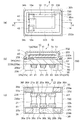
図1は、第1実施形態の水晶振動子の概略構成を示す模式図である。図1(a)は、リッド(蓋体)側から見た平面図であり、図1(b)は、図1(a)のA−A線での断面図であり、図1(c)は、底面側から見た平面図である。なお、図1(a)では、リッドを省略してある。また、分かり易くするために、各構成要素の寸法比率は実際と異なる。
図2は、第1実施形態の水晶振動子に搭載された電子素子を含む水晶振動子の駆動に関わる回路図である。
(First embodiment)
First, a crystal resonator as an example of a vibrating device will be described.
FIG. 1 is a schematic diagram illustrating a schematic configuration of the crystal resonator according to the first embodiment. 1A is a plan view seen from the lid (lid) side, and FIG. 1B is a cross-sectional view taken along line AA in FIG. 1A, and FIG. These are the top views seen from the bottom face side. In FIG. 1A, the lid is omitted. In addition, for easy understanding, the dimensional ratio of each component is different from the actual one.
FIG. 2 is a circuit diagram relating to driving of a crystal resonator including an electronic element mounted on the crystal resonator of the first embodiment.
図1に示すように、水晶振動子1は、振動片としての水晶振動片10と、複数の電子素子としての、温度センサーとして機能する感温素子であるサーミスター20及び抵抗(第1の抵抗)21と、水晶振動片10、サーミスター20及び抵抗21が搭載(収納)された容器としてのパッケージ30と、を備えている。換言すれば、水晶振動子1は、図2の回路図の破線で囲んだ範囲内の回路構成要素がパッケージ30に搭載されている。
As shown in FIG. 1, a
水晶振動片10は、例えば、水晶の原石などから所定の角度で切り出されたATカット型であって、平面形状が略矩形に形成され、厚みすべり振動が励振される振動部11と振動部11に接続された基部12とを一体で有している。
水晶振動片10は、振動部11の一方の主面13及び他方の主面14に形成された略矩形の励振電極15,16から引き出された引き出し電極15a,16aが、基部12に形成されている。
引き出し電極15aは、一方の主面13の励振電極15から、水晶振動片10の長手方向(紙面左右方向)に沿って基部12に引き出され、基部12の側面に沿って他方の主面14に回り込み、他方の主面14の励振電極16の近傍まで延在している。
引き出し電極16aは、他方の主面14の励振電極16から、水晶振動片10の長手方向に沿って基部12に引き出され、基部12の側面に沿って一方の主面13に回り込み、一方の主面13の励振電極15の近傍まで延在している。
励振電極15,16及び引き出し電極15a,16aは、例えば、Crを下地層とし、その上にAuが積層された構成の金属被膜となっている。
The quartz
The quartz
The lead electrode 15 a is drawn from the
The lead electrode 16 a is drawn from the
The
サーミスター20は、例えば、チップ型(直方体形状)の感温素子(感温抵抗素子)であって、一対の電極20a,20bを長手方向の両端に有し、温度変化に対して電気抵抗の変化の大きい抵抗体である。
サーミスター20には、例えば、温度の上昇に対して抵抗が減少するNTC(Negative Temperature Coefficient)サーミスターと呼ばれるサーミスターが用いられている。NTCサーミスターは、温度の変化に対する抵抗値の変化が比例的なため、温度センサーとして多用されている。
The
As the
サーミスター20は、パッケージ30に収納され、水晶振動片10近傍の温度を検出することにより、温度センサーとして水晶振動片10の温度変化に伴う周波数変動の補正に資する機能を果たしている。
サーミスター20は、上述したように水晶振動片10近傍の温度をより正確に検出するために、電子機器において水晶振動子1から離れて配置されたICチップ内に集積化されることなく、外付け部品として水晶振動子1に搭載されている。
ここで、図2に示すように、サーミスター20は、水晶振動片10に対して電気的に独立しており、水晶振動片10とは電気的に接続されておらず、非接続となっている。
The
As described above, the
Here, as shown in FIG. 2, the
抵抗21は、例えば、チップ型(直方体形状)の抵抗体であって、一対の電極21a,21bを長手方向の両端に有し、図2に示すように、分圧抵抗としてサーミスター20と電源との間に直列に接続されている。
具体的には、例えば、電源電圧が3.0V、サーミスター20の抵抗値が100kΩの場合に、抵抗値が100kΩの抵抗21を電源とサーミスター20との間に直列に接続することにより、サーミスター20と抵抗21との間の電圧を半分の1.5Vに分圧することができる。
この抵抗21は、電子機器のICチップ内に集積化されてしまうと、サーミスター20の抵抗値などの特性ばらつきや仕様変更に対する調整(抵抗値変更など)が困難となることから、仕様に応じて適宜、最適な抵抗値を選択可能とするために外付け部品として水晶振動子1に搭載されている。
ここで、図2に示すように、抵抗21は、水晶振動片10とは電気的に非接続となっている。
The
Specifically, for example, when the power supply voltage is 3.0 V and the
If the
Here, as shown in FIG. 2, the
図1に戻って、パッケージ30は、平面形状が略矩形で略平板状の容器体としてのパッケージベース31と、パッケージベース31の一方側を覆う平板状の蓋体としてのリッド32と、を有し、略直方体形状に形成されている。
パッケージベース31には、セラミックグリーンシートを成形して積層し焼成した酸化アルミニウム質焼結体、水晶、ガラス、シリコン(高抵抗シリコン)などが用いられている。
リッド32には、パッケージベース31と同材料、または、コバール、42アロイ、ステンレス鋼などの金属が用いられている。
なお、リッド32に樹脂を使用する場合には、シールド性を確保するために、リッド32の主面(表面)が金属のメッキや導電性を有する膜によって覆われたものを用いることが好ましい。
Returning to FIG. 1, the
The
The
In addition, when using resin for the
パッケージベース31の一方側の主面である第1主面33には、水晶振動片10が搭載される第1凹部34が設けられ、第1主面33の反対側の他方側の主面である第2主面35には、サーミスター20及び抵抗21が収納される凹状の収納部としての第2凹部36が設けられている。
第1凹部34及び第2凹部36は、平面形状が略矩形であって、それぞれ第1主面33及び第2主面35の略中央部に設けられている。なお、水晶振動子1は、パッケージベース31の第1凹部34と第2凹部36とが、平面視で重なるように設けられていることにより、パッケージ30の小型化が図られている。
The first
The
パッケージベース31の第1凹部34の底面34aには、水晶振動片10の引き出し電極15a,16aに対向する位置に、内部端子34b,34cが設けられている。
水晶振動片10は、引き出し電極15a,16aが、金属フィラーなどの導電性物質が混合された、エポキシ系、シリコーン系、ポリイミド系などの導電性接着剤40を介して内部端子34b,34cに接合されている。これにより、水晶振動片10は、第1主面33側の第1凹部34に搭載されたこととなる。
In the quartz
水晶振動子1は、水晶振動片10がパッケージベース31の内部端子34b,34cに接合された状態で、パッケージベース31の第1凹部34がリッド32により覆われ、パッケージベース31とリッド32とがシームリング、低融点ガラス、接着剤などの接合部材38で接合されることにより、パッケージベース31の第1凹部34が気密に封止されている。
なお、パッケージベース31の気密に封止された第1凹部34内は、減圧された真空状態(真空度の高い状態)または窒素、ヘリウム、アルゴンなどの不活性ガスが充填された状態となっている。
In the
Note that the hermetically sealed
パッケージベース31の第2凹部36の底面36aには、サーミスター20の電極20a,20bに対向する位置に電極パッド36b,36cが設けられ、抵抗21の電極21a,21bに対向する位置に電極パッド36d,36eが設けられている。
サーミスター20は、電極20a,20bがハンダ、導電性接着剤などの接合部材41を介して電極パッド36b,36cに接合されている。抵抗21は、電極21a,21bが接合部材41を介して電極パッド36d,36eに接合されている。
これにより、サーミスター20及び抵抗21は、第2凹部36に収納されたこととなる。なお、電極パッド36bと電極パッド36dとは互いに接続されている。
ここで、サーミスター20及び抵抗21は、長手方向(ここでは、電極20a(21a)と電極20b(21b)とを結ぶ方向)がパッケージベース31の長手方向(紙面左右方向)と交差するように(ここでは、直交するように)配置されている。
On the
In the
Thereby, the
Here, the
パッケージベース31の第2主面35の4隅には、それぞれ矩形状の電極端子37a,37b,37c,37dが設けられ、長手方向に沿って設けられた電極端子37bと電極端子37cとの中間には電極端子37eが設けられている。
5つの電極端子37a〜37eのうち、例えば、一方の対角に位置する2つの電極端子37b,37dは、図示しない内部配線により水晶振動片10の引き出し電極15a,16aに繋がる内部端子34b,34cと接続されている。
Among the five
他方の対角に位置する2つの電極端子37a,37cは、電極端子37aが、導通ビア(金属などの導通部材が充填されているスルーホール)36g、内部配線36f(電極パッド36d)を経由して、サーミスター20の電極20aに繋がる電極パッド36bと接続され、電極端子37cが、導通ビア36i、内部配線36hを経由して、サーミスター20の電極20bに繋がる電極パッド36cと接続されている。
残りの電極端子37eは、導通ビア36k、内部配線36jを経由して、抵抗21の電極21bに繋がる電極パッド36eと接続されている。なお、上述したように、サーミスター20の電極20a(電極パッド36b)と抵抗21の電極21a(電極パッド36d)とは互いに接続されている。
The two
The remaining
なお、パッケージ30のリッド32が金属製の場合には、接合部材38に導電性の材料を用い、電極端子37cが、導通ビア36i、内部配線36h、導通ビア36m、接合部材38を経由してリッド32と電気的に接続されていることが好ましい。
この電極端子37cは、サーミスター20のアース側(GND側)の電極20bに接続され、アース端子(GND端子)となっている。
なお、電極端子37cとリッド32との電気的な接続には、パッケージベース31の外側の角部に、パッケージベース31の厚み方向に沿って形成された図示しないキャスタレーション(凹部)に設けられた導電膜を用いてもよい。
When the
The
For the electrical connection between the
内部端子34b,34c、電極パッド36b〜36e、電極端子37a〜37eは、例えば、W、Moなどのメタライズ層にNi、Auなどの各被膜をメッキなどにより積層した金属被膜からなる。
The
図2に示すように、水晶振動子1は、例えば、電子機器のICチップ内に集積化された発振回路から、電極端子37b,37dを経由して印加される駆動信号によって、水晶振動片10が厚みすべり振動を励振されて所定の周波数で共振(発振)し、電極端子37b,37dから共振信号(発振信号)を出力する。
この際、水晶振動子1は、サーミスター20が温度センサーとして水晶振動片10近傍の温度を検出し、電極端子37eを経由して電源から供給された電源電圧を抵抗21により分圧した電圧値の変化として、電極端子37aから出力する。
As shown in FIG. 2, the
At this time, the
水晶振動子1の電極端子37aから出力された電圧信号は、例えば、電子機器のICチップ内に集積化されたA/D変換回路によりA/D変換されて温度補償回路に入力される。そして、温度補償回路は、入力された電圧信号に応じて温度補償データに基づいた補正信号を発振回路に出力する。
発振回路は、入力された補正信号に基づいて補正された駆動信号を水晶振動片10に印加し、温度変化に伴い変動する水晶振動片10の共振周波数を、所定の周波数になるように補正する。
The voltage signal output from the
The oscillation circuit applies a drive signal corrected based on the input correction signal to the quartz
上述したように、本実施形態の水晶振動子1は、第1主面33側に水晶振動片10が搭載され、第2主面35の第2凹部36にサーミスター20及び抵抗21が収納されたパッケージベース31を備えている。そして、水晶振動子1は、パッケージベース31の第2主面35に、水晶振動片10またはサーミスター20及び抵抗21と接続された複数(ここでは、5つ)の電極端子37a〜37eが設けられ、サーミスター20及び抵抗21が、水晶振動片10と電気的に非接続となっている。
As described above, in the
これにより、水晶振動子1は、水晶振動片10近傍のより正確な温度の検出や、調整作業の難しさなどの理由で、電子機器のICチップ内に集積化しにくく、且つ、水晶振動片10と電気的に非接続のサーミスター20及び抵抗21を、第2凹部36に収納することができる。
この結果、水晶振動子1は、第2凹部36を有効利用することができ、実装される電子機器(例えば、携帯電話など)の小型化に寄与することができる。
As a result, the
As a result, the
また、水晶振動子1は、パッケージベース31の平面形状が矩形に形成され、サーミスター20及び抵抗21の長手方向がパッケージベース31の長手方向と直交するように配置されていることから、パッケージベース31の反り(傾向的に長手方向の反りが大きい)に対するサーミスター20及び抵抗21の固定強度(接合強度)の低下を抑制することができる。
Further, since the
また、水晶振動子1は、第1主面33側が水晶振動片10を覆う金属製のリッド32により気密に封止され、電極端子37a〜37eのうち、電極端子37cがリッド32と電気的に接続されていることから、外部からのノイズや静電気などに対するシールド性能を向上させることができる。
加えて、水晶振動子1は、リッド32と電気的に接続されている電極端子37cが、アース端子(GND端子)であることから、電極端子37cが接地されることにより、シールド性能を更に向上させることができる。
The
In addition, since the
また、水晶振動子1は、第2凹部36に収納された2つの電子素子のうち、1つがサーミスター20であることから、水晶振動片10が搭載されたパッケージベース31内に収納されたサーミスター20によって、サーミスター20がパッケージベース31外に配置されている場合よりも、水晶振動片10の温度を正確に検出することができる。
Further, in the
また、水晶振動子1は、第2凹部36に収納された2つの電子素子のうち、残りの1つがサーミスター20と電気的に接続されている抵抗21であることから、水晶振動片10が搭載されたパッケージベース31の温度変化を電圧値の変化として検出する温度検出回路の主要な構成要素を、パッケージベース31の第2凹部36にまとめて収納することができる。この結果、水晶振動子1は、実装される電子機器(例えば、携帯電話など)の回路構成のユニット化に寄与することができる。
Further, in the
(変形例)
次に、第1実施形態の変形例について説明する。
図3は、第1実施形態の変形例の水晶振動子の概略構成を示す模式図である。図3(a)は、リッド側から見た平面図であり、図3(b)は、図3(a)のA−A線での断面図であり、図3(c)は、底面側から見た平面図である。
なお、第1実施形態との共通部分には、同一符号を付して詳細な説明を省略し、第1実施形態と異なる部分を中心に説明する。
(Modification)
Next, a modification of the first embodiment will be described.
FIG. 3 is a schematic diagram illustrating a schematic configuration of a crystal resonator according to a modification of the first embodiment. 3A is a plan view seen from the lid side, FIG. 3B is a cross-sectional view taken along line AA in FIG. 3A, and FIG. It is the top view seen from.
In addition, the same code | symbol is attached | subjected to a common part with 1st Embodiment, detailed description is abbreviate | omitted, and it demonstrates centering on a different part from 1st Embodiment.
図3に示すように、変形例の水晶振動子2は、第1実施形態と比較して、パッケージ130の第1主面133側の構成が異なる。
水晶振動子2は、パッケージベース131の第1主面133が凹部のない平坦な面で構成され、この第1主面133に水晶振動片10を搭載する内部端子34b,34cが設けられている。
As shown in FIG. 3, the
In the
水晶振動子2は、パッケージベース131の第1主面133側が水晶振動片10を覆う金属製の蓋体としてのリッド132により気密に封止されている。リッド132は、コバール、42アロイ、ステンレス鋼などの金属を用いて、全周につば部132aが設けられたキャップ状に形成されている。
水晶振動子2は、リッド132のキャップ部分の膨らみにより、水晶振動片10の振動が可能な内部空間が確保されている。
リッド132は、つば部132aがシームリング、ろう材、導電性接着剤などの導電性接合部材138を介してパッケージベース131の第1主面133に接合されている。
水晶振動子2は、上記内部空間が第1実施形態と同様に、減圧された真空状態(真空度の高い状態)または窒素、ヘリウム、アルゴンなどの不活性ガスが充填された状態となっている。
In the
In the
The
In the
上述したように、水晶振動子2は、パッケージベース131の第1主面133が凹部のない平坦な面で構成されていることから、例えば、セラミックグリーンシートを一層減らせるなど、パッケージベース131の構造を第1実施形態と比較して簡素化することができる。
この結果、水晶振動子2は、パッケージベース131の製造が容易となり、製造コストを削減することができる。
As described above, in the
As a result, the
(第2実施形態)
次に、第2実施形態の振動デバイスの一例としての水晶振動子について説明する。
図4は、第2実施形態の水晶振動子の概略構成を示す模式図である。図4(a)は、リッド側から見た平面図であり、図4(b)は、図4(a)のA−A線での断面図であり、図4(c)は、底面側から見た平面図である。図5は、第2実施形態の水晶振動子に搭載された電子素子を含む水晶振動子の駆動に関わる回路図である。
なお、第1実施形態との共通部分には、同一符号を付して詳細な説明を省略し、第1実施形態と異なる部分を中心に説明する。
(Second Embodiment)
Next, a crystal resonator as an example of the vibration device according to the second embodiment will be described.
FIG. 4 is a schematic diagram illustrating a schematic configuration of the crystal resonator according to the second embodiment. 4A is a plan view seen from the lid side, FIG. 4B is a cross-sectional view taken along line AA in FIG. 4A, and FIG. It is the top view seen from. FIG. 5 is a circuit diagram relating to driving of a crystal resonator including an electronic element mounted on the crystal resonator of the second embodiment.
In addition, the same code | symbol is attached | subjected to a common part with 1st Embodiment, detailed description is abbreviate | omitted, and it demonstrates centering on a different part from 1st Embodiment.
図4、図5に示すように、第2実施形態の水晶振動子3は、第1実施形態と比較して、パッケージ230におけるパッケージベース231の第2主面35側の構成及び回路構成(電子素子の数)が異なる。
水晶振動子3は、パッケージベース231の第2主面35側に、パッケージベース231の長手方向(紙面左右方向)に沿って延びる一対の脚部239a,239bを備え、一方の脚部239aと他方の脚部239bとの間に、凹状の収納部としての第2凹部236が設けられている。
As shown in FIGS. 4 and 5, the
The
水晶振動子3は、第2凹部236に、サーミスター20及び抵抗21に加えて、電子素子としての抵抗(第2の抵抗)22が収納されている。
抵抗22は、抵抗21と同様に、例えば、チップ型(直方体形状)の抵抗体であって、一対の電極22a,22bを長手方向の両端に有し、図5に示すように、平滑用抵抗としてサーミスター20と並列に接続される。
In the
The
抵抗22は、サーミスター20の温度変化に対する分圧された電圧値の変化の線形性(リニアリティー)を向上させるために用いられている。これにより、水晶振動子3は、水晶振動片10近傍の温度変化の情報がより正確に温度補償回路に伝達されることとなる。
この抵抗22は、電子機器のICチップ内に集積化されてしまうと、サーミスター20の抵抗値などの特性ばらつきや仕様変更に対する調整(抵抗値変更など)が困難となることから、外付け部品として水晶振動子3に搭載されている。
ここで、図5に示すように、抵抗22は、水晶振動片10とは電気的に非接続となっている。
The
If the
Here, as shown in FIG. 5, the
図4に戻って、パッケージベース231の第2凹部236の底面236aには、サーミスター20及び抵抗21用の電極パッド36b,36c,36d,36eに加えて、抵抗22の電極22a,22bに対向する位置に電極パッド36n,36pが設けられている。
抵抗22は、電極22a,22bが接合部材41を介して電極パッド36n,36pに接合されている。なお、電極パッド36nは、電極パッド36bと接続され、電極パッド36pは、電極パッド36cと接続されている。これにより、抵抗22は、サーミスター20と並列に接続されていることとなる。
Returning to FIG. 4, the
In the
これにより、水晶振動子3は、サーミスター20及び抵抗21,22が第2凹部236に収納されたこととなる。
ここで、サーミスター20及び抵抗21,22は、第1実施形態と同様に、長手方向(ここでは、電極20a(21a,22a)と電極20b(21b,22b)とを結ぶ方向)が、パッケージベース231の長手方向と交差するように(ここでは、直交するように)配置されている。
As a result, in the
Here, the
上述したように、水晶振動子3は、パッケージベース231が第2主面35側に一対の脚部239a,239bを備え、一方の脚部239aと他方の脚部239bとの間に第2凹部236が設けられていることから、例えば、枠状に囲まれた第1実施形態の第2凹部36よりも収納スペースが広くなり、より多くの電子素子(サーミスター20及び抵抗21に加えて抵抗22)を収納することができる。
As described above, in the
また、水晶振動子3は、一方の脚部239aと他方の脚部239bとの間に第2凹部236が設けられており、換言すれば、枠状に囲まれた収納部(例えば、第1実施形態の第2凹部36)の対向する2つの壁が開口されていることになる。これにより、水晶振動子3は、第2凹部236の通気性が向上し、サーミスター20及び抵抗21,22の発熱による第2凹部236の温度上昇を抑制することができる。
この結果、水晶振動子3は、水晶振動片10が搭載されている第1主面33側と、サーミスター20が収納されている第2凹部236側との温度差が少なくなることから、水晶振動片10の温度をより正確に検出することができる。
In addition, the
As a result, the
(変形例)
次に、第2実施形態の変形例について説明する。
図6は、第2実施形態の変形例の水晶振動子の概略構成を示す模式図である。図6(a)は、リッド側から見た平面図であり、図6(b)は、図6(a)のA−A線での断面図であり、図6(c)は、底面側から見た平面図である。
なお、第2実施形態との共通部分には、同一符号を付して詳細な説明を省略し、第2実施形態と異なる部分を中心に説明する。
(Modification)
Next, a modification of the second embodiment will be described.
FIG. 6 is a schematic diagram illustrating a schematic configuration of a crystal resonator according to a modification of the second embodiment. 6A is a plan view seen from the lid side, FIG. 6B is a cross-sectional view taken along line AA in FIG. 6A, and FIG. 6C is a bottom side. It is the top view seen from.
In addition, the same code | symbol is attached | subjected to a common part with 2nd Embodiment, detailed description is abbreviate | omitted, and it demonstrates centering on a different part from 2nd Embodiment.
図6に示すように、変形例の水晶振動子4は、第2実施形態と比較して、パッケージ330の第1主面333側の構成が異なる。
水晶振動子4は、パッケージベース331の第1主面333が凹部のない平坦な面で構成され、この第1主面333に水晶振動片10を搭載する内部端子34b,34cが設けられている。
As shown in FIG. 6, the crystal resonator 4 according to the modification is different in the configuration on the first
In the crystal resonator 4, the first
水晶振動子4は、パッケージベース331の第1主面333側が水晶振動片10を覆う金属製の蓋体としてのリッド232により気密に封止されている。リッド232は、コバール、42アロイ、ステンレス鋼などの金属を用いて、全周につば部232aが設けられたキャップ状に形成されている。
水晶振動子4は、リッド232のキャップ部分の膨らみにより、水晶振動片10の振動が可能な内部空間が確保されている。
リッド232は、つば部232aがシームリング、ろう材、導電性接着剤などの導電性接合部材238を介してパッケージベース331の第1主面333に接合されている。
水晶振動子4は、上記内部空間が第2実施形態と同様に、減圧された真空状態(真空度の高い状態)または窒素、ヘリウム、アルゴンなどの不活性ガスが充填された状態となっている。
In the crystal resonator 4, the first
In the crystal resonator 4, an internal space in which the
The
In the crystal unit 4, the internal space is in a reduced vacuum state (high vacuum state) or in a state filled with an inert gas such as nitrogen, helium, or argon, as in the second embodiment. .
上述したように、水晶振動子4は、パッケージベース331の第1主面333が凹部のない平坦な面で構成されていることから、例えば、セラミックグリーンシートを一層減らせるなど、パッケージベース331の構造を第2実施形態と比較して簡素化することができる。
この結果、水晶振動子4は、パッケージベース331の製造が容易となり、製造コストを削減することができる。
As described above, since the first
As a result, the crystal unit 4 can easily manufacture the
(第3実施形態)
次に、上述した水晶振動子を備えた電子機器として、携帯電話を一例に挙げて説明する。
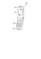
図7は、第3実施形態の携帯電話を示す模式斜視図である。
携帯電話700は、上記各実施形態及び各変形例の水晶振動子を備えた携帯電話である。
図7に示す携帯電話700は、上述した水晶振動子(1〜4のいずれか)を、例えば、基準クロック発振源などのタイミングデバイスとして用い、更に液晶表示装置701、複数の操作ボタン702、受話口703、及び送話口704を備えて構成されている。なお、携帯電話700の形態は、図示のタイプに限定されるものではなく、いわゆるスマートフォンタイプでもよい。
(Third embodiment)
Next, a mobile phone will be described as an example of an electronic device including the above-described crystal resonator.
FIG. 7 is a schematic perspective view showing the mobile phone of the third embodiment.
A
A
上述した水晶振動子などの振動デバイスは、上記携帯電話に限らず、電子ブック、パーソナルコンピューター、テレビ、デジタルスチールカメラ、ビデオカメラ、ビデオレコーダー、ナビゲーション装置、ページャー、電子手帳、電卓、ワードプロセッサー、ワークステーション、テレビ電話、POS端末、タッチパネルを備えた機器などのタイミングデバイスとして好適に用いることができ、いずれの場合にも上記各実施形態及び各変形例で説明した効果を奏する電子機器を提供することができる。 The above-described vibrating devices such as the crystal resonator are not limited to the above-described mobile phones, but include electronic books, personal computers, televisions, digital still cameras, video cameras, video recorders, navigation devices, pagers, electronic notebooks, calculators, word processors, and workstations. It is possible to provide an electronic device that can be suitably used as a timing device such as a device including a video phone, a POS terminal, and a touch panel, and that has the effects described in the above embodiments and modifications in any case. it can.
なお、携帯電話700に代表される電子機器は、前述したように上記水晶振動子(1〜4のいずれか)の水晶振動片10を駆動する発振回路と、水晶振動片10の温度変化に伴う周波数変動を補正する温度補償回路と、を備えていることが好ましい。
これによれば、携帯電話700に代表される電子機器は、水晶振動片10を駆動する発振回路と共に、水晶振動片10の温度変化に伴う周波数変動を補正する温度補償回路を備えていることから、発振回路が発振する共振周波数を温度補償することができ、温度特性に優れた電子機器を提供することができる。
Note that an electronic device typified by the
According to this, an electronic device typified by the
なお、振動片の形状は、図示した平板状のタイプに限定されるものではなく、中央部が厚く周辺部が薄いタイプ(コンベックスタイプ、ベベルタイプ、メサタイプ)、逆に中央部が薄く周辺部が厚いタイプ(逆メサタイプ)などでもよい。
なお、振動片の材料としては、水晶に限定されるものではなく、タンタル酸リチウム(LiTaO3)、四ホウ酸リチウム(Li2B4O7)、ニオブ酸リチウム(LiNbO3)、チタン酸ジルコン酸鉛(PZT)、酸化亜鉛(ZnO)、窒化アルミニウム(AlN)などの圧電体、またはシリコン(Si)などの半導体でもよい。
また、厚みすべり振動の駆動方法は、圧電体の圧電効果によるものの他に、クーロン力による静電駆動であってもよい。
The shape of the resonator element is not limited to the flat plate type shown in the figure, but the central part is thick and the peripheral part is thin (convex type, bevel type, mesa type). Conversely, the central part is thin and the peripheral part is thin. A thick type (reverse mesa type) may be used.
The material of the resonator element is not limited to quartz, but lithium tantalate (LiTaO 3 ), lithium tetraborate (Li 2 B 4 O 7 ), lithium niobate (LiNbO 3 ), zirconate titanate A piezoelectric material such as lead acid (PZT), zinc oxide (ZnO), and aluminum nitride (AlN), or a semiconductor such as silicon (Si) may be used.
Further, the driving method of the thickness shear vibration may be electrostatic driving by Coulomb force in addition to the piezoelectric effect of the piezoelectric body.
1,2,3,4…振動デバイスとしての水晶振動子、10…振動片としての水晶振動片、11…振動部、12…基部、13…一方の主面、14…他方の主面、15,16…励振電極、15a,16a…引き出し電極、20…電子素子としてのサーミスター、20a,20b…電極、21,22…電子素子としての抵抗、21a,21b,22a,22b…電極、30…パッケージ、31…容器体としてのパッケージベース、32…蓋体としてのリッド、33…第1主面、34…第1凹部、34a…底面、34b,34c…内部端子、35…第2主面、36…収納部としての第2凹部、36a…底面、36b,36c,36d,36e,36n,36p…電極パッド、36f,36h,36j…内部配線、36g,36i,36k,36m…導通ビア、37a,37b,37c,37d,37e…電極端子、38…接合部材、40…導電性接着剤、41…接合部材、130…パッケージ、131…パッケージベース、132…リッド、132a…つば部、133…第1主面、138…導電性接合部材、230…パッケージ、231…パッケージベース、232…リッド、232a…つば部、236…第2凹部、236a…底面、238…導電性接合部材、239a,239b…脚部、330…パッケージ、331…パッケージベース、700…携帯電話、701…液晶表示装置、702…操作ボタン、703…受話口、704…送話口。
DESCRIPTION OF
Claims (11)
複数の電子素子と、
第1主面側に前記振動片が搭載され、前記第1主面の反対側の第2主面に設けられた凹状の収納部に前記複数の電子素子が収納された容器体と、を備え、
前記容器体の前記第2主面側には、前記振動片または複数の前記電子素子と接続された複数の電極端子が設けられ、
前記複数の電子素子は、前記振動片と電気的に非接続であることを特徴とする振動デバイス。 A vibrating piece,
A plurality of electronic elements;
A container body in which the vibrating element is mounted on the first main surface side, and the plurality of electronic elements are stored in a concave storage portion provided on the second main surface opposite to the first main surface. ,
A plurality of electrode terminals connected to the vibrating piece or the plurality of electronic elements are provided on the second main surface side of the container body,
The vibration device, wherein the plurality of electronic elements are electrically disconnected from the vibration piece.
一方の前記脚部と他方の前記脚部との間に前記収納部が配置されていることを特徴とする振動デバイス。 The vibrating device according to claim 1, wherein the container body includes a pair of legs on the second main surface side,
The vibration device, wherein the storage portion is disposed between the one leg portion and the other leg portion.
複数の前記電子素子は、長手方向が前記容器体の長手方向と交差するように配置されていることを特徴とする振動デバイス。 The vibrating device according to claim 1 or 2, wherein the container body has a rectangular planar shape,
The plurality of electronic elements are arranged so that a longitudinal direction intersects a longitudinal direction of the container body.
前記第1主面側は、前記振動片を覆う金属製の蓋体、または少なくともいずれかの主面が導電膜で覆われている蓋体により気密に封止され、
前記電極端子の少なくとも1つは、前記金属製の蓋体または前記導電膜と電気的に接続されていることを特徴とする振動デバイス。 The vibrating device according to any one of claims 1 to 3,
The first main surface side is hermetically sealed by a metal lid that covers the resonator element, or at least one main surface is covered with a conductive film,
At least one of the electrode terminals is electrically connected to the metal lid or the conductive film.
前記金属製の蓋体または前記導電膜と電気的に接続されている前記電極端子は、アース端子であることを特徴とする振動デバイス。 The vibrating device according to claim 4,
The vibration device, wherein the electrode terminal electrically connected to the metal lid or the conductive film is a ground terminal.
前記複数の電子素子の少なくとも1つは、サーミスターであることを特徴とする振動デバイス。 The vibrating device according to any one of claims 1 to 5,
At least one of the plurality of electronic elements is a thermistor.
前記サーミスターを除いた残りの前記複数の電子素子は、前記サーミスターと電気的に接続されている抵抗であることを特徴とする振動デバイス。 The vibrating device according to claim 6,
The remaining plurality of electronic elements excluding the thermistor are resistors electrically connected to the thermistor.
電源と、
前記振動片を駆動する発振回路と、
前記振動片の温度変化に伴う周波数変動を補正する温度補償回路と、
を備えたことを特徴とする電子機器。 The electronic device according to claim 8,
Power supply,
An oscillation circuit for driving the resonator element;
A temperature compensation circuit that corrects a frequency variation associated with a temperature change of the resonator element;
An electronic device characterized by comprising:
前記残りの前記電子素子のうち少なくとも第1の抵抗は、一対の電極を備え、
前記第1の抵抗の一方の前記電極は前記電源に電気的に接続され、
一対の電極を備える前記サーミスターの一方の前記電極は前記アース端子に電気的に接続され、
前記第1の抵抗の他方の前記電極は前記サーミスターの他方の前記電極と電気的に接続され、
前記第1の抵抗の他方の前記電極及び前記サーミスターの他方の前記電極は、
A(アナログ)/D(デジタル)変換回路を介して前記温度補償回路に電気的に接続されていることを特徴とする電子機器。 The electronic device according to claim 9,
At least a first resistor of the remaining electronic elements includes a pair of electrodes,
One electrode of the first resistor is electrically connected to the power source;
One of the thermistors comprising a pair of electrodes is electrically connected to the ground terminal;
The other electrode of the first resistor is electrically connected to the other electrode of the thermistor;
The other electrode of the first resistor and the other electrode of the thermistor are:
An electronic apparatus characterized by being electrically connected to the temperature compensation circuit via an A (analog) / D (digital) conversion circuit.
前記残りの前記電子素子のうち第2の抵抗は、前記サーミスターと電気的に並列に接続されていることを特徴とする電子機器。 The electronic device according to claim 10,
Of the remaining electronic elements, a second resistor is electrically connected in parallel with the thermistor.
Priority Applications (1)
| Application Number | Priority Date | Filing Date | Title |
|---|---|---|---|
| JP2011229468A JP2013090176A (en) | 2011-10-19 | 2011-10-19 | Vibration device and electronic apparatus |
Applications Claiming Priority (1)
| Application Number | Priority Date | Filing Date | Title |
|---|---|---|---|
| JP2011229468A JP2013090176A (en) | 2011-10-19 | 2011-10-19 | Vibration device and electronic apparatus |
Publications (2)
| Publication Number | Publication Date |
|---|---|
| JP2013090176A true JP2013090176A (en) | 2013-05-13 |
| JP2013090176A5 JP2013090176A5 (en) | 2014-11-06 |
Family
ID=48533662
Family Applications (1)
| Application Number | Title | Priority Date | Filing Date |
|---|---|---|---|
| JP2011229468A Withdrawn JP2013090176A (en) | 2011-10-19 | 2011-10-19 | Vibration device and electronic apparatus |
Country Status (1)
| Country | Link |
|---|---|
| JP (1) | JP2013090176A (en) |
Cited By (7)
| Publication number | Priority date | Publication date | Assignee | Title |
|---|---|---|---|---|
| JP2018019214A (en) * | 2016-07-27 | 2018-02-01 | 京セラ株式会社 | Crystal oscillator |
| JP2018019211A (en) * | 2016-07-27 | 2018-02-01 | 京セラ株式会社 | Crystal oscillator |
| JP2018037700A (en) * | 2016-08-29 | 2018-03-08 | 京セラ株式会社 | Crystal oscillator |
| JP2018037699A (en) * | 2016-08-29 | 2018-03-08 | 京セラ株式会社 | Crystal oscillator |
| JP2019134226A (en) * | 2018-01-29 | 2019-08-08 | 京セラ株式会社 | Crystal oscillator |
| CN111106810A (en) * | 2018-10-26 | 2020-05-05 | 京瓷株式会社 | Piezoelectric device |
| JP2021010152A (en) * | 2019-07-03 | 2021-01-28 | 京セラ株式会社 | Crystal device |
-
2011
- 2011-10-19 JP JP2011229468A patent/JP2013090176A/en not_active Withdrawn
Cited By (8)
| Publication number | Priority date | Publication date | Assignee | Title |
|---|---|---|---|---|
| JP2018019214A (en) * | 2016-07-27 | 2018-02-01 | 京セラ株式会社 | Crystal oscillator |
| JP2018019211A (en) * | 2016-07-27 | 2018-02-01 | 京セラ株式会社 | Crystal oscillator |
| JP2018037700A (en) * | 2016-08-29 | 2018-03-08 | 京セラ株式会社 | Crystal oscillator |
| JP2018037699A (en) * | 2016-08-29 | 2018-03-08 | 京セラ株式会社 | Crystal oscillator |
| JP2019134226A (en) * | 2018-01-29 | 2019-08-08 | 京セラ株式会社 | Crystal oscillator |
| CN111106810A (en) * | 2018-10-26 | 2020-05-05 | 京瓷株式会社 | Piezoelectric device |
| CN111106810B (en) * | 2018-10-26 | 2023-08-22 | 京瓷株式会社 | piezoelectric device |
| JP2021010152A (en) * | 2019-07-03 | 2021-01-28 | 京セラ株式会社 | Crystal device |
Similar Documents
| Publication | Publication Date | Title |
|---|---|---|
| JP6183156B2 (en) | Package, vibrating device, oscillator, electronic equipment and mobile object | |
| JP6618675B2 (en) | Vibrating device, electronic device, and moving object | |
| JP2013146003A (en) | Vibration device and electronic apparatus | |
| JP2013090176A (en) | Vibration device and electronic apparatus | |
| JP5866973B2 (en) | Method for manufacturing vibration device | |
| JP2016127467A (en) | Vibration device, electronic apparatus and mobile object | |
| JP2016010099A (en) | Composite electronic component, oscillator, electronic apparatus and mobile | |
| JP5862155B2 (en) | Vibration device and electronic equipment | |
| JP2014107778A (en) | Vibration device, electronic apparatus and mobile body | |
| JP2014068098A (en) | Vibration piece, vibration device, electronic apparatus and moving body | |
| JP2016129288A (en) | Electronic device, electronic apparatus and mobile | |
| JP2013146004A (en) | Vibration device and electronic apparatus | |
| JP5668392B2 (en) | Piezoelectric vibration element, piezoelectric vibrator and piezoelectric oscillator | |
| US8525606B2 (en) | Vibrator element, vibrator, oscillator, and electronic device | |
| JP6137255B2 (en) | Vibration device and electronic equipment | |
| JP6635151B2 (en) | Vibration device and electronic equipment | |
| JP2014050067A (en) | Vibration device, electronic equipment, and mobile device | |
| JP2016127437A (en) | Electronic device, electronic apparatus and mobile | |
| JP6780688B2 (en) | Vibration devices, electronic devices and mobiles | |
| JP6816813B2 (en) | Vibration devices and electronic devices | |
| JP2012134824A (en) | Vibrating reed, vibrator, oscillator and electronic apparatus | |
| JP2013070313A (en) | Vibration device and electronic apparatus | |
| JP6369592B2 (en) | Vibration device and electronic equipment | |
| JP2012090083A (en) | Vibration device and electronic apparatus | |
| JP2017017569A (en) | Vibration piece, vibration device, electronic apparatus and movable body |
Legal Events
| Date | Code | Title | Description |
|---|---|---|---|
| A521 | Written amendment |
Free format text: JAPANESE INTERMEDIATE CODE: A523 Effective date: 20140924 |
|
| A621 | Written request for application examination |
Free format text: JAPANESE INTERMEDIATE CODE: A621 Effective date: 20140924 |
|
| RD04 | Notification of resignation of power of attorney |
Free format text: JAPANESE INTERMEDIATE CODE: A7424 Effective date: 20150107 |
|
| A977 | Report on retrieval |
Free format text: JAPANESE INTERMEDIATE CODE: A971007 Effective date: 20150914 |
|
| A131 | Notification of reasons for refusal |
Free format text: JAPANESE INTERMEDIATE CODE: A131 Effective date: 20150925 |
|
| A761 | Written withdrawal of application |
Free format text: JAPANESE INTERMEDIATE CODE: A761 Effective date: 20151111 |