JP2012168448A - 光ファイバ - Google Patents
光ファイバ Download PDFInfo
- Publication number
- JP2012168448A JP2012168448A JP2011030942A JP2011030942A JP2012168448A JP 2012168448 A JP2012168448 A JP 2012168448A JP 2011030942 A JP2011030942 A JP 2011030942A JP 2011030942 A JP2011030942 A JP 2011030942A JP 2012168448 A JP2012168448 A JP 2012168448A
- Authority
- JP
- Japan
- Prior art keywords
- optical fiber
- layer
- hole
- refractive index
- core
- Prior art date
- Legal status (The legal status is an assumption and is not a legal conclusion. Google has not performed a legal analysis and makes no representation as to the accuracy of the status listed.)
- Granted
Links
- 239000013307 optical fiber Substances 0.000 title claims abstract description 150
- 238000009826 distribution Methods 0.000 claims abstract description 47
- 238000005452 bending Methods 0.000 claims description 38
- 238000005253 cladding Methods 0.000 claims description 23
- 239000011148 porous material Substances 0.000 claims description 3
- 230000005540 biological transmission Effects 0.000 description 14
- 238000010586 diagram Methods 0.000 description 13
- 239000000463 material Substances 0.000 description 13
- 239000010453 quartz Substances 0.000 description 12
- VYPSYNLAJGMNEJ-UHFFFAOYSA-N silicon dioxide Inorganic materials O=[Si]=O VYPSYNLAJGMNEJ-UHFFFAOYSA-N 0.000 description 12
- 239000000470 constituent Substances 0.000 description 9
- 230000003287 optical effect Effects 0.000 description 9
- 239000012535 impurity Substances 0.000 description 6
- 230000009022 nonlinear effect Effects 0.000 description 6
- 239000000835 fiber Substances 0.000 description 5
- 239000004038 photonic crystal Substances 0.000 description 4
- 230000000694 effects Effects 0.000 description 3
- 238000004519 manufacturing process Methods 0.000 description 3
- 239000007787 solid Substances 0.000 description 3
- ZOXJGFHDIHLPTG-UHFFFAOYSA-N Boron Chemical compound [B] ZOXJGFHDIHLPTG-UHFFFAOYSA-N 0.000 description 2
- PXGOKWXKJXAPGV-UHFFFAOYSA-N Fluorine Chemical compound FF PXGOKWXKJXAPGV-UHFFFAOYSA-N 0.000 description 2
- XAGFODPZIPBFFR-UHFFFAOYSA-N aluminium Chemical compound [Al] XAGFODPZIPBFFR-UHFFFAOYSA-N 0.000 description 2
- 229910052782 aluminium Inorganic materials 0.000 description 2
- 229910052796 boron Inorganic materials 0.000 description 2
- 239000006185 dispersion Substances 0.000 description 2
- 229910052731 fluorine Inorganic materials 0.000 description 2
- 239000011737 fluorine Substances 0.000 description 2
- 229910052732 germanium Inorganic materials 0.000 description 2
- GNPVGFCGXDBREM-UHFFFAOYSA-N germanium atom Chemical compound [Ge] GNPVGFCGXDBREM-UHFFFAOYSA-N 0.000 description 2
- 238000000034 method Methods 0.000 description 2
- 238000010438 heat treatment Methods 0.000 description 1
- 230000002093 peripheral effect Effects 0.000 description 1
- 238000003672 processing method Methods 0.000 description 1
- 239000011800 void material Substances 0.000 description 1
Images


Landscapes
- Optical Fibers, Optical Fiber Cores, And Optical Fiber Bundles (AREA)
Abstract
【解決手段】コア部2と、前記コア部2を包囲し、前記コア部2の屈折率よりも低い屈折率のクラッド部3と、を備える光ファイバ1であって、前記クラッド部3は、内部に設けられる複数個の空孔部5が前記コア部2に対して周回状に形成された第1と第2の空孔部層51,52と、を備える。前記コア部2の実効屈折率分布が一番高く、前記第1の空孔部層51の実効屈折率分布が一番小さくなるように空孔部5を構成して、屈折率分布がW型分布となるように形成したので、従来の光ファイバよりも大きな実効断面積を実現できる。
【選択図】図1
Description
(1)光ファイバ1の構造
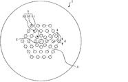
図1及び図2は本願発明の第1実施形態に係る光ファイバ1の断面構造を示す概略図である。ここで、図1及び図2において、1は光ファイバ、2はコア部、3はクラッド部、4は空孔部、5は空孔部層(第1の層51,第2の層52)である。
次に、図1及び図2に示した本願発明に係る光ファイバ1の諸特性の一例について説明する。
Δ(%)=(n1 2−n2 2)/(2×n1 2) ……(I)
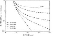
なお、式(I)における計算では、国際標準であるITU−T G.656で推奨される曲げ損失及び遮断波長の条件を満たすよう設計されている。つまり、かかるITU−T G.656に準拠して、遮断波長を1450nm以下とし、基本モードの曲げ損失を、曲げ半径30mmにおいて0.5dB/100turns(ターンズ:巻き数)以下としている。なお、遮断波長は、前記した非特許文献1に記載される条件である、光ファイバ1を敷設した時の実効的な曲げ半径と考えられる140mmの曲げ半径に対して第1高次モードの損失が1dB/mとなる波長としている。
以上説明したように、本実施形態に係る光ファイバ1は、空孔構造を有する光ファイバ1において、コア部2の屈折率がクラッド部3の屈折率より高く、クラッド部3に形成される空孔部層5が2層以上形成されている。よって、本実施形態の光ファイバは、従来の光ファイバよりも大きな実効断面積を実現することができる。
(1)光ファイバ1の構造
図12は、第2実施形態に係る光ファイバ1の断面構造を示した概略図である。
なお、以下の説明では、すでに第1実施形態で説明した部分と同一あるいは略同一である部分等は、共通する符号を付して説明を省略する。また、空孔部4の外径の大きさの範囲、空孔部層5の配置、光ファイバ1の構成材料や製造方法等についても、第1実施形態と共通するので、説明を省略する。
以上説明したように、本実施形態に係る光ファイバ1は、空孔構造を有する光ファイバ1において、コア部2の屈折率がクラッド部3の屈折率より高く、また、クラッド部3に形成される空孔部層5が2層以上形成されている。よって、本実施形態の光ファイバは、従来の光ファイバよりも大きな実効断面積を実現することができる。
2: コア部
3: クラッド部
4: 空孔部
5: 空孔部層
51:空孔部層(第1の層)
52:空孔部層(第2の層)
53:空孔部層(第3の層)
Claims (9)
- コア部と、
前記コア部を包囲し、前記コア部の屈折率よりも低い屈折率のクラッド部と、
前記クラッド部の内部で、光ファイバ軸方向に連続的且つ光ファイバ軸方向に直交する断面で離散的に設けられる複数個の空孔部が前記コア部に対して周回状に形成された2層以上の空孔部層と、
を備える光ファイバ。 - 前記コア部に最も近い空孔部層が、前記コア部に最も近い空孔部層の外側にある空孔部層より実効屈折率分布が小さいことを特徴とする請求項1に記載の光ファイバ。
- 前記コア部に最も近い空孔部層が、前記外側にある空孔部層より空孔部占有率が大きいことを特徴とする請求項1又は2に記載の光ファイバ。
- 前記空孔部が前記光ファイバ軸方向に直交する断面形状が円形であり、
前記コア部に最も近い空孔部層を構成する前記空孔部の直径が、前記外側にある空孔部層を構成する前記空孔部の直径より大きいことを特徴とする請求項1から3のいずれかに記載の光ファイバ。 - 前記コア部に最も近い空孔部層が、前記外側にある空孔部層より空孔部分布密度が大きいことを特徴とする請求項1から4のいずれかに記載の光ファイバ。
- 前記空孔部が、前記コア部を中心として円環状または正多角形状に配置されて形成されることを特徴とする請求項1から5のいずれかに記載の光ファイバ。
- 光が伝搬する面積である光ファイバの実効断面積160μm2以上、210μm2以下であることを特徴とする請求項1から6のいずれかに記載の光ファイバ。
- 遮断波長が、1450nm以下であることを特徴とする請求項1から7のいずれかに記載の光ファイバ。
- 1450nm以上1625nm以下の波長の光に対して、曲げ半径30mmにおける曲げ損失が0.5dB/100turns以下であることを特徴とする請求項1から8のいずれかに記載の光ファイバ。
Priority Applications (1)
| Application Number | Priority Date | Filing Date | Title |
|---|---|---|---|
| JP2011030942A JP5660673B2 (ja) | 2011-02-16 | 2011-02-16 | 光ファイバ |
Applications Claiming Priority (1)
| Application Number | Priority Date | Filing Date | Title |
|---|---|---|---|
| JP2011030942A JP5660673B2 (ja) | 2011-02-16 | 2011-02-16 | 光ファイバ |
Publications (2)
| Publication Number | Publication Date |
|---|---|
| JP2012168448A true JP2012168448A (ja) | 2012-09-06 |
| JP5660673B2 JP5660673B2 (ja) | 2015-01-28 |
Family
ID=46972640
Family Applications (1)
| Application Number | Title | Priority Date | Filing Date |
|---|---|---|---|
| JP2011030942A Active JP5660673B2 (ja) | 2011-02-16 | 2011-02-16 | 光ファイバ |
Country Status (1)
| Country | Link |
|---|---|
| JP (1) | JP5660673B2 (ja) |
Cited By (1)
| Publication number | Priority date | Publication date | Assignee | Title |
|---|---|---|---|---|
| WO2017098878A1 (ja) * | 2015-12-10 | 2017-06-15 | 日本電信電話株式会社 | フォトニック結晶ファイバ及びハイパワー光伝送システム |
Citations (8)
| Publication number | Priority date | Publication date | Assignee | Title |
|---|---|---|---|---|
| JPH1095628A (ja) * | 1996-05-31 | 1998-04-14 | Lucent Technol Inc | 微細構造光ファイバ含有製品と微細構造光ファイバ製造法 |
| WO2001063328A1 (fr) * | 2000-02-28 | 2001-08-30 | Sumitomo Electric Industries, Ltd. | Fibre optique |
| JP2003337239A (ja) * | 2002-05-17 | 2003-11-28 | Nippon Telegr & Teleph Corp <Ntt> | 分散シフト光ファイバ |
| JP2004220026A (ja) * | 2003-01-13 | 2004-08-05 | Sumitomo Electric Ind Ltd | 微細構造光ファイバとそれを用いた光ファイバテープ心線・光コネクタ・光ファイバアレイ・光接続部材 |
| WO2006098470A1 (ja) * | 2005-03-18 | 2006-09-21 | The Furukawa Electric Co., Ltd. | 光ファイバおよび導波路 |
| WO2010023881A1 (ja) * | 2008-08-26 | 2010-03-04 | 株式会社フジクラ | ファイバヒューズ遮断部材、ファイバレーザ、および光伝送路 |
| JP2010217472A (ja) * | 2009-03-17 | 2010-09-30 | Nippon Telegr & Teleph Corp <Ntt> | 空孔構造光ファイバ及びこれを用いた光伝送システム |
| JP2011027866A (ja) * | 2009-07-23 | 2011-02-10 | Nippon Telegr & Teleph Corp <Ntt> | 空孔構造光ファイバ |
-
2011
- 2011-02-16 JP JP2011030942A patent/JP5660673B2/ja active Active
Patent Citations (8)
| Publication number | Priority date | Publication date | Assignee | Title |
|---|---|---|---|---|
| JPH1095628A (ja) * | 1996-05-31 | 1998-04-14 | Lucent Technol Inc | 微細構造光ファイバ含有製品と微細構造光ファイバ製造法 |
| WO2001063328A1 (fr) * | 2000-02-28 | 2001-08-30 | Sumitomo Electric Industries, Ltd. | Fibre optique |
| JP2003337239A (ja) * | 2002-05-17 | 2003-11-28 | Nippon Telegr & Teleph Corp <Ntt> | 分散シフト光ファイバ |
| JP2004220026A (ja) * | 2003-01-13 | 2004-08-05 | Sumitomo Electric Ind Ltd | 微細構造光ファイバとそれを用いた光ファイバテープ心線・光コネクタ・光ファイバアレイ・光接続部材 |
| WO2006098470A1 (ja) * | 2005-03-18 | 2006-09-21 | The Furukawa Electric Co., Ltd. | 光ファイバおよび導波路 |
| WO2010023881A1 (ja) * | 2008-08-26 | 2010-03-04 | 株式会社フジクラ | ファイバヒューズ遮断部材、ファイバレーザ、および光伝送路 |
| JP2010217472A (ja) * | 2009-03-17 | 2010-09-30 | Nippon Telegr & Teleph Corp <Ntt> | 空孔構造光ファイバ及びこれを用いた光伝送システム |
| JP2011027866A (ja) * | 2009-07-23 | 2011-02-10 | Nippon Telegr & Teleph Corp <Ntt> | 空孔構造光ファイバ |
Cited By (7)
| Publication number | Priority date | Publication date | Assignee | Title |
|---|---|---|---|---|
| WO2017098878A1 (ja) * | 2015-12-10 | 2017-06-15 | 日本電信電話株式会社 | フォトニック結晶ファイバ及びハイパワー光伝送システム |
| JPWO2017098878A1 (ja) * | 2015-12-10 | 2018-06-07 | 日本電信電話株式会社 | フォトニック結晶ファイバ及びハイパワー光伝送システム |
| CN108292010A (zh) * | 2015-12-10 | 2018-07-17 | 日本电信电话株式会社 | 光子晶体光纤及高功率光传送系统 |
| US10539784B2 (en) | 2015-12-10 | 2020-01-21 | Nippon Telegraph And Telephone Corporation | Photonic crystal fiber and high-power light transmission system |
| US10545333B2 (en) | 2015-12-10 | 2020-01-28 | Nippon Telegraph And Telephone Corporation | Photonic crystal fiber and high-power light transmission system |
| EP3929638A1 (en) * | 2015-12-10 | 2021-12-29 | Nippon Telegraph And Telephone Corporation | Photonic crystal fiber and high-power light transmission system |
| EP3929639A1 (en) * | 2015-12-10 | 2021-12-29 | Nippon Telegraph And Telephone Corporation | Photonic crystal fiber and high-power light transmission system |
Also Published As
| Publication number | Publication date |
|---|---|
| JP5660673B2 (ja) | 2015-01-28 |
Similar Documents
| Publication | Publication Date | Title |
|---|---|---|
| JP5916525B2 (ja) | マルチコアファイバ | |
| JP6177994B2 (ja) | マルチコアファイバ | |
| JP3854627B2 (ja) | 空孔付き単一モード光ファイバ | |
| US8965165B2 (en) | Multicore fiber | |
| JP5311417B2 (ja) | 光ファイバ製造方法並びに光ファイバ母材及びその製造方法 | |
| WO2013035708A1 (ja) | 通信用マルチコアファイバ | |
| JP3786010B2 (ja) | 光ファイバ | |
| JP6057340B2 (ja) | マルチコア光ファイバ | |
| JP5468711B2 (ja) | マルチコアファイバ | |
| JP6340342B2 (ja) | マルチコアファイバ | |
| JP2011033899A (ja) | ホーリーファイバ | |
| JP5605630B2 (ja) | 光ファイバ | |
| JP6578017B2 (ja) | フォトニック結晶ファイバ及びハイパワー光伝送システム | |
| JP5118107B2 (ja) | 空孔構造光ファイバ | |
| JP2012014081A (ja) | ホーリーファイバ | |
| JP5660673B2 (ja) | 光ファイバ | |
| JP5557290B2 (ja) | 光ファイバ | |
| JP5430679B2 (ja) | 光ファイバ | |
| WO2022034662A1 (ja) | マルチコア光ファイバ及び設計方法 | |
| JP5356466B2 (ja) | ホーリーファイバ | |
| JP3917613B2 (ja) | フォトニック結晶光ファイバ | |
| JP6048890B2 (ja) | 光ファイバ | |
| JP2010217472A (ja) | 空孔構造光ファイバ及びこれを用いた光伝送システム | |
| JP2006243423A (ja) | フォトニック結晶ファイバ、光伝送路および光通信システム | |
| JP5481735B2 (ja) | 光ファイバ |
Legal Events
| Date | Code | Title | Description |
|---|---|---|---|
| A621 | Written request for application examination |
Free format text: JAPANESE INTERMEDIATE CODE: A621 Effective date: 20130603 |
|
| A521 | Request for written amendment filed |
Free format text: JAPANESE INTERMEDIATE CODE: A523 Effective date: 20130603 |
|
| A977 | Report on retrieval |
Free format text: JAPANESE INTERMEDIATE CODE: A971007 Effective date: 20131220 |
|
| A131 | Notification of reasons for refusal |
Free format text: JAPANESE INTERMEDIATE CODE: A131 Effective date: 20140107 |
|
| A521 | Request for written amendment filed |
Free format text: JAPANESE INTERMEDIATE CODE: A523 Effective date: 20140218 |
|
| A131 | Notification of reasons for refusal |
Free format text: JAPANESE INTERMEDIATE CODE: A131 Effective date: 20140826 |
|
| A521 | Request for written amendment filed |
Free format text: JAPANESE INTERMEDIATE CODE: A523 Effective date: 20141015 |
|
| TRDD | Decision of grant or rejection written | ||
| A01 | Written decision to grant a patent or to grant a registration (utility model) |
Free format text: JAPANESE INTERMEDIATE CODE: A01 Effective date: 20141125 |
|
| A61 | First payment of annual fees (during grant procedure) |
Free format text: JAPANESE INTERMEDIATE CODE: A61 Effective date: 20141128 |
|
| R150 | Certificate of patent or registration of utility model |
Ref document number: 5660673 Country of ref document: JP Free format text: JAPANESE INTERMEDIATE CODE: R150 |
|
| R250 | Receipt of annual fees |
Free format text: JAPANESE INTERMEDIATE CODE: R250 |
|
| R250 | Receipt of annual fees |
Free format text: JAPANESE INTERMEDIATE CODE: R250 |
|
| R250 | Receipt of annual fees |
Free format text: JAPANESE INTERMEDIATE CODE: R250 |
|
| R250 | Receipt of annual fees |
Free format text: JAPANESE INTERMEDIATE CODE: R250 |
|
| R250 | Receipt of annual fees |
Free format text: JAPANESE INTERMEDIATE CODE: R250 |
|
| R250 | Receipt of annual fees |
Free format text: JAPANESE INTERMEDIATE CODE: R250 |
|
| R250 | Receipt of annual fees |
Free format text: JAPANESE INTERMEDIATE CODE: R250 |