JP2012144261A - Transport tray - Google Patents
Transport tray Download PDFInfo
- Publication number
- JP2012144261A JP2012144261A JP2011002248A JP2011002248A JP2012144261A JP 2012144261 A JP2012144261 A JP 2012144261A JP 2011002248 A JP2011002248 A JP 2011002248A JP 2011002248 A JP2011002248 A JP 2011002248A JP 2012144261 A JP2012144261 A JP 2012144261A
- Authority
- JP
- Japan
- Prior art keywords
- suction
- devices
- tray
- cutting
- holding
- Prior art date
- Legal status (The legal status is an assumption and is not a legal conclusion. Google has not performed a legal analysis and makes no representation as to the accuracy of the status listed.)
- Pending
Links
Images


Landscapes
- Supply And Installment Of Electrical Components (AREA)
- Packaging Frangible Articles (AREA)
- Container, Conveyance, Adherence, Positioning, Of Wafer (AREA)
- Dicing (AREA)
- Packages (AREA)
Abstract
【課題】デバイスの大きさに関係なく、しかもデバイスを治具から搬送トレイへ効率よく移し替ることが可能な搬送トレイを提供する。
【解決手段】複数のデバイスを収容して搬送する搬送トレイであって、複数のデバイスを支持する表面を有するデバイス支持部と、デバイス支持部の外周を囲繞して形成された枠部とを備えたトレイ本体と、トレイ本体のデバイス支持部の表面に装着されタック力を有するタック層とを具備している。
【選択図】図8A transport tray capable of efficiently transferring a device from a jig to a transport tray regardless of the size of the device is provided.
A transport tray that accommodates and transports a plurality of devices, and includes a device support portion having a surface that supports the plurality of devices, and a frame portion that surrounds the outer periphery of the device support portion. A tray body, and a tack layer attached to the surface of the device support portion of the tray body and having tack force.
[Selection] Figure 8
Description
本発明は、切削装置等のダイシング装置によって分割された半導体デバイスを収容して搬送する搬送トレイに関する。 The present invention relates to a transport tray that houses and transports semiconductor devices divided by a dicing apparatus such as a cutting apparatus.
半導体デバイス製造工程においては、略円板形状である半導体ウエーハの表面に格子状に配列された多数の領域にIC、LSI等のデバイスを形成し、該デバイスが形成された各領域を区画する分割予定ラインに沿って切断することにより個々のデバイスを製造している。このようにして分割されたデバイスは、パッケージングされて携帯電話やパソコン等の電気機器に広く利用されている。 In the semiconductor device manufacturing process, devices such as ICs and LSIs are formed in a large number of regions arranged in a lattice pattern on the surface of a substantially wafer-shaped semiconductor wafer, and each region where the devices are formed is partitioned. Individual devices are manufactured by cutting along planned lines. Devices divided in this way are packaged and widely used in electric devices such as mobile phones and personal computers.
携帯電話やパソコン等の電気機器はより軽量化、小型化が求められており、半導体デバイスのパッケージもチップサイズパッケージ(CSP)と称する小型化できるパッケージ技術が開発されている。CSP技術の一つとして、Quad Flat Non−lead Package(QFN)と称するパッケージ技術が実用化されている。このQFNと称するパッケージ技術は、デバイスの接続端子に対応した接続端子が複数形成されているとともにデバイス毎に区画する分割予定ラインが格子状に形成された銅板等の金属板に複数個のデバイスをマトリックス状に配設し、デバイスの裏面側から樹脂をモールディングした樹脂部によって金属板とデバイスを一体化することによりCSP基板(パッケージ基板)を形成する。このパッケージ基板を分割予定ラインに沿って切断することにより、個々にパッケージされたデバイス(チップサイズパッケージ)に分割する。 Electrical devices such as mobile phones and personal computers are required to be lighter and smaller, and a package technology capable of reducing the size of a semiconductor device package called a chip size package (CSP) has been developed. As one of the CSP technologies, a package technology called Quad Flat Non-Lead Package (QFN) has been put into practical use. This package technology called QFN is a method in which a plurality of devices are provided on a metal plate such as a copper plate in which a plurality of connection terminals corresponding to the connection terminals of the device are formed and the division lines to be divided for each device are formed in a lattice shape. A CSP substrate (package substrate) is formed by integrating the metal plate and the device with a resin portion that is arranged in a matrix and molded with resin from the back side of the device. The package substrate is cut along a predetermined division line to divide the package substrate into individually packaged devices (chip size packages).
上記パッケージ基板の切断は、一般に切削ブレードを備えた切削装置によって施される。この切削装置は、分割予定ラインと対応する領域に切削ブレードの切れ刃を逃がす逃がし溝が格子状に形成されるとともに逃がし溝によって区画された複数の領域にそれぞれ吸引孔が設けられた治具を備え、保持テーブル上に位置付けられた該治具にパッケージ基板を吸引保持し、切削ブレードを回転させつつ保持テーブルをパッケージ基板の分割予定ラインに沿って相対移動することにより、パッケージ基板を分割予定ラインに沿って切断し、個々のデバイスに分割する。その後、個々に分割されたデバイスは、複数の収容室を備えた搬送トレイに収容されて組立工程に搬送される(例えば特許文献1参照)。 The package substrate is generally cut by a cutting apparatus having a cutting blade. This cutting apparatus is provided with jigs in which relief grooves for escaping the cutting blade of the cutting blade are formed in a lattice shape in an area corresponding to the division line, and suction holes are provided in a plurality of areas partitioned by the relief grooves. The package substrate is sucked and held by the jig positioned on the holding table, and the holding table is relatively moved along the planned dividing line of the package substrate while rotating the cutting blade, thereby dividing the package substrate into the planned dividing line. Cut along and split into individual devices. Thereafter, the individually divided devices are stored in a transfer tray having a plurality of storage chambers and transferred to an assembly process (see, for example, Patent Document 1).
而して、搬送トレイに設けられた複数の収容室はデバイス(チップサイズパッケージ)の大きさに対応してそれぞれ隔壁によって区画されており、従ってデバイスの大きさに対応した種類の搬送トレイを用意しなければならず、管理が煩雑になるという問題がある。
また、個々に分割されたデバイスを1個ずつ治具から搬送トレイに移し替えなければならず、この移し替え工程に時間を要し、生産性の面で必ずしも満足し得るものではない。
Thus, the plurality of storage chambers provided in the transport tray are partitioned by partition walls corresponding to the size of the device (chip size package), and accordingly, a transport tray of a type corresponding to the size of the device is prepared. There is a problem that management is complicated.
In addition, each of the divided devices must be transferred from the jig to the transport tray one by one, and this transfer process takes time and is not necessarily satisfactory in terms of productivity.
本発明は上記事実に鑑みてなされたものであり、その主たる技術的課題は、デバイスの大きさに関係なく、しかもデバイスを治具から搬送トレイへ効率よく移し替ることが可能な搬送トレイを提供することにある。 The present invention has been made in view of the above facts, and its main technical problem is to provide a transport tray that can efficiently transfer a device from a jig to a transport tray regardless of the size of the device. There is to do.
上記主たる技術課題を解決するため、本発明によれば、複数のデバイスを収容して搬送する搬送トレイであって、
複数のデバイスを支持する表面を有するデバイス支持部と、該デバイス支持部の外周を囲繞して形成された枠部とを備えたトレイ本体と、
該トレイ本体のデバイス支持部の表面に装着されタック力を有するタック層と、を具備している、
ことを特徴とする搬送トレイが提供される。
In order to solve the main technical problem, according to the present invention, a transport tray that accommodates and transports a plurality of devices,
A tray body including a device support portion having a surface for supporting a plurality of devices, and a frame portion formed to surround the outer periphery of the device support portion;
A tack layer attached to the surface of the device support portion of the tray body and having tack force,
The conveyance tray characterized by this is provided.
該トレイ本体のデバイス支持部およびタック層は、光透過性を有していることが望ましい。 It is desirable that the device support portion and the tack layer of the tray main body have optical transparency.
本発明による搬送トレイは、複数のデバイスを支持する表面を有するデバイス支持部と、該デバイス支持部の外周を囲繞して形成された枠部とを備えたトレイ本体と、該トレイ本体のデバイス支持部の表面に装着されタック力を有するタック層とを具備しているので、個々のデバイスに対応して区画された複数の収容室を設ける必要がなく、個々のデバイスの大きさに対応した種類のトレイを用意する必要がない。従って、1種類の搬送トレイで各種のデバイスに対応することができ、管理が簡素化する。また、本発明による搬送トレイはデバイス支持部の表面にタック力を有するタック層が装着されているので、切削装置等のダイシング装置によって個々の分割された複数のデバイスをデバイス搬送装置によって一括してタック層上に移し替えることが可能であり、生産性を向上することができる。 A transport tray according to the present invention includes a tray main body including a device support portion having a surface for supporting a plurality of devices, a frame portion formed so as to surround an outer periphery of the device support portion, and a device support for the tray main body. Since it has a tack layer that is attached to the surface of the unit and has tack force, it is not necessary to provide a plurality of storage chambers that are partitioned corresponding to individual devices, and the type corresponding to the size of each device There is no need to prepare a tray. Accordingly, various types of devices can be handled with one type of transport tray, and management is simplified. In addition, since the transport tray according to the present invention is provided with a tack layer having a tack force on the surface of the device support portion, a plurality of devices divided by a dicing apparatus such as a cutting apparatus are collectively collected by the device transport apparatus. It can be transferred onto the tack layer, and productivity can be improved.
以下、本発明に従って構成された搬送トレイの好適な実施形態について、添付図面を参照して、更に詳細に説明する。 DESCRIPTION OF EMBODIMENTS Hereinafter, a preferred embodiment of a transport tray configured according to the present invention will be described in more detail with reference to the accompanying drawings.
図1の(a)および(b)には、被加工物としてのパッケージ基板の斜視図および断面図が示されている。図1の(a)および(b)に示すパッケージ基板1は金属板11を具備し、金属板11の表面11aに所定の方向に延びる複数の第1の分割予定ライン111と、該第1の分割予定ライン111と直交する方向に延びる第2の分割予定ライン112が格子状に形成されている。第1の分割予定ライン111と第2の分割予定ライン112によって区画された複数の領域にそれぞれデバイス(チップサイズパッケージ)113が配置されており、このデバイス113は金属板11の裏面側から合成樹脂部12によってモールディングされている。このように形成されたパッケージ基板1は、第1の分割予定ライン111および第2の分割予定ライン112に沿って切断され個々にパッケージされたデバイス113に分割される。
1A and 1B show a perspective view and a cross-sectional view of a package substrate as a workpiece. A package substrate 1 shown in FIGS. 1A and 1B includes a
上記パッケージ基板1を複数の第1の分割予定ライン111および第2の分割予定ライン112に沿って切断するには、図2の(a)および(b)に示すように保持治具2によって保持される。
保持治具2は、図2の(a)に示すように矩形状に形成され表面中央部に上記パッケージ基板1を吸引保持する吸引保持部20が突出して設けられている。吸引保持部20の上面(保持面)にはパッケージ基板1に形成された第1の分割予定ライン111および第2の分割予定ライン112と対応する領域に後述する切削ブレードの切れ刃を逃がす逃がし溝21および22が格子状に形成されている。また、吸引保持部材20には、第1の分割予定ライン111および第2の分割予定ライン112によって区画された複数の領域にそれぞれ吸引孔23が形成されており、この吸引孔23が図示しない吸引手段に連通されるようになっている。なお、保持治具2の4隅には、位置決め用の穴24が設けられている。このように構成された保持治具2には、図2の(b)に示すように吸引保持部20の上面(保持面)に上記パッケージ基板1が載置される。
In order to cut the package substrate 1 along the plurality of
As shown in FIG. 2A, the
次に、上述した保持路具2に載置されたパッケージ基板1を第1の分割予定ライン111および第2の分割予定ライン112に沿って切断する切削装置について、図3を参照して説明する。
図3に示す切削装置3は、略直方体状の装置ハウジング31を具備している。この装置ハウジング31内には、被加工物を保持する吸引テーブル32が切削送り方向である矢印Xで示す方向に移動可能に配設されている。吸引テーブル32の上面には吸引凹部321が設けられており、この吸引凹部321に図示しない吸引手段と連通する吸引口322が開口している。また、吸引テーブル32の上面における4隅には、上記保持治具2の4隅に設けられた位置決め用の穴24が嵌合する位置きめピン323が立設されている。また、吸引テーブル32は、図示しない回転機構によって回転可能に構成されている。このように構成された吸引テーブル32は、図示しない切削送り手段によって、矢印Xで示す切削送り方向に移動せしめられるようになっている。
Next, a cutting apparatus that cuts the package substrate 1 placed on the above-described
The
切削装置3は、切削手段としてのスピンドルユニット33を具備している。スピンドルユニット33は、図示しない割り出し送り手段によって図3において矢印Yで示す割り出し送り方向に移動せしめられるとともに、図示しない切り込み送り手段によって図3において矢印Zで示す切り込み送り方向に移動せしめられるようになっている。このスピンドルユニット33は、図示しない移動基台に装着され割り出し方向である矢印Yで示す方向および切り込み方向である矢印Zで示す方向に移動調整されるスピンドルハウジング331と、該スピンドルハウジング331に回転自在に支持された回転スピンドル332と、該回転スピンドル332の前端部に装着された切削ブレード333とを具備している。
The
また、切削装置3は、上記吸引テーブル32上に保持された被加工物の表面を撮像し、上記切削ブレード333によって切削すべき領域を検出するための撮像手段34を具備している。この撮像手段34は、顕微鏡からなる光学系と撮像素子(CCD)を具備しており、撮像した画像信号を図示しない制御手段に送る。
Further, the
図3に示す切削装置3は以上のように構成されており、以下切削装置3を用いて上記パッケージ基板1を複数の第1の分割予定ライン111および第2の分割予定ライン112に沿って切断する切断作業について説明する。
先ず、切削装置3の吸引テーブル32上にパッケージ基板1が載置され保持路具2を載置する。このとき、保持路具2の4隅に設けられた複数の位置決め用の穴24を吸引テーブル32の4隅に配設された位置決めピン323に嵌合することにより、パッケージ基板1が載置され保持路具2は所定の位置に位置付けられる。そして、図示しない吸引手段を作動することにより、吸引テーブル32の吸引口322、吸引凹部321、保持治具2に設けられた複数の吸引孔23を介して保持治具2の吸引保持部20に載置されたパッケージ基板1の各デバイス113に負圧が作用し、パッケージ基板1の各デバイス113が保持治具2の吸引保持部20上に吸引保持される(パッケージ基板保持工程)。
The
First, the package substrate 1 is placed on the suction table 32 of the
上記パッケージ基板保持工程を実施したならば、図示しない切削送り手段を作動してパッケージ基板1を保持した保持治具2を撮像手段34の直下まで移動せしめる。保持治具2が撮像手段34の直下に位置付けられると、撮像手段34および図示しない制御手段によってパッケージ基板1の切削加工すべき加工領域を検出するアライメント作業を実行する。即ち、撮像手段34および図示しない制御手段は、パッケージ基板1の所定方向に形成されている第1の分割予定ライン111と、第1の分割予定ライン111に沿って切削する切削ブレード333との位置合わせを行うためのパターンマッチング等の画像処理を実行し、切削加工すべき加工領域のアライメントを遂行する。また、パッケージ基板1に形成されている上記所定方向に対して直交する方向に延びる第2の分割予定ライン112に対しても、同様に切削加工すべき加工領域のアライメントが遂行される。
When the package substrate holding step is performed, the cutting feed means (not shown) is operated to move the holding
上述したように、パッケージ基板1の切削加工すべき加工領域を検出するアライメント作業を実行したならば、保持治具2を切削領域に移動し、図4の(a)に示すように所定の第1の分割予定ライン111の一端を切削ブレード333の直下より図4の(a)において僅かに右側に位置付ける。そして、切削ブレード333を矢印333aで示す方向に回転しつつ図示しない切込み送り手段を作動して切削ブレード333を矢印Z1で示す方向に所定量切り込み送りし、所定の切り込み深さに位置付ける。この切り込み深さは、切削ブレード333の切れ刃の外周縁が保持治具2の吸引保持部20に形成された逃がし溝21(図2の(a)参照)に達する位置に設定されている。次に、図示しない切削送り手段を作動して吸引テーブル32を図4の(a)において矢印X1で示す方向に所定の切削送り速度で移動する。そして、吸引テーブル32に保持治具2を介して保持されたパッケージ基板1の所定の第1の分割予定ライン111の他端が図4の(b)に示すように切削ブレード333の直下より僅かに左側に達したら、吸引テーブル32の移動を停止するとともに、切削ブレード333を矢印Z2で示す方向に上昇せしめ、次に切削すべき第1の分割予定ライン111に割り出し送りして切削作業を繰り返す。この結果、パッケージ基板1は、第1の分割予定ライン111に沿って切断される(第1の切断工程)。
As described above, when the alignment operation for detecting the machining area to be cut of the package substrate 1 is executed, the holding
上述した第1の切断工程を実施したならば、吸引テーブル32を90度回動し、吸引テーブル32に保持治具2を介して保持されたパッケージ基板1に形成された第2の分割予定ライン112を切削送り方向である矢印Xで示す方向に位置付ける、そして、パッケージ基板1に対して上記第1の切断工程を同様に全ての第2の分割予定ライン112に沿って切断作業を実施する(第2の切断工程)。
If the 1st cutting process mentioned above was implemented, the suction table 32 will be rotated 90 degree | times, and the 2nd division | segmentation schedule line formed in the package board | substrate 1 hold | maintained through the holding
以上のようにして第1の切断工程および第2の切断工程が実施されたパッケージ基板1は、図5に示すように第1の分割予定ライン111および第2の分割予定ライン112に沿って切断され、個々のデバイス(チップサイズパッケージ)113に分割される。このようにして分割された個々のデバイス113は、保持治具2の吸引保持部20に吸引保持された状態で維持される。
The package substrate 1 that has been subjected to the first cutting step and the second cutting step as described above is cut along the first scheduled
上述したように分割されたデバイス113は、後述する搬送トレイに収容されて次工程である組立工程に移送される。ここで、本発明に従って構成された搬送トレイについて、図6および図7を参照して説明する。
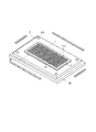
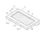
図6および図7に示す搬送トレイ5は、矩形状のトレイ本体51と、該トレイ本体51の表面に装着されたタック層52とからなっている。トレイ本体51は光透過性を有する合成樹脂(例えば、アクリル樹脂)によって形成されており、上記複数のデバイス(チップサイズパッケージ)113を支持する表面511aを有するデバイス支持部511と、該デバイス支持部511の外周を囲繞して形成された枠部512とを備えている。デバイス支持部511は、トレイ本体51の上面に形成された矩形状の凹部を有し、該矩形状の凹部の底面が複数のデバイス113を支持する表面511aとして機能する。このデバイス支持部511の底面には、短手方向両側に図示しない搬送装置の支持部材と係合する2個の係合凹部511b、511bがそれぞれ設けられている(図6には一方の側の係合凹部511b、511bのみが示されている)。このように形成されたデバイス支持部511の表面511aにタック層52が装着される。タック層52は、タック力を有するシートからなっている。タック力を有するシートとしては、新タック化成株式会社が製造販売する商品名「セパレス」または「ハンデコタック」を用いることができる。このように構成された搬送トレイ5は、トレイ本体51のデバイス支持部511およびタック層52が光透過性を有していることが望ましい。
The
The
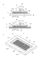
次に、図5に示すように個々に分割された複数のデバイス(チップサイズパッケージ)113を保持治具2の吸引保持部20上から搬送トレイ5に収容する方法について、図8を参照して説明する。
複数のデバイス113を保持治具2の吸引保持部20上から搬送トレイ5に収容するには、図示の実施形態においてはデバイス搬送装置6を用いて実施する。デバイス搬送装置6は、複数のデバイスを吸引保持する吸引保持パッド61と、該吸引保持パッド61を一端部に支持する搬送アーム62を具備しており、搬送アーム62が図示しない作動機構によって作動せしめられる。吸引保持パッド61は、下面に上記複数のデバイス113を形成するパッケージ基板1と同様に大きさの矩形状の凹部611aを備えたパッド本体611と、該パッド本体711の凹部611aに嵌合された吸着パッド612とからなっている。パッド本体611は、中央部には上記凹部611aに連通する吸引口611bが設けられている。この吸引口611bは、図示しない吸引手段に連通されている。上記吸着パッド612は矩形状に形成されており、上記保持治具2の吸引保持部20に設けられた吸引孔23と同様に複数のデバイス113と対応する位置に複数の吸引孔612aが設けられている。従って、図示しない吸引手段が作動すると、吸引口611bおよび凹部611aを介して複数の吸引孔612aに負圧が作用せしめられる。
Next, referring to FIG. 8, a method for accommodating a plurality of devices (chip size packages) 113 that are individually divided as shown in FIG. 5 from the
In order to accommodate a plurality of
上述したデバイス搬送装置6を用いて複数のデバイス113を保持治具2の吸引保持部20上から搬送トレイ5に収容するには、図8の(a)に示すように図示しない作動機構を作動して吸引保持パッド61の吸着パッド612の下面を保持治具2の吸引保持部20上に載置されている複数のデバイス113の上面に位置付ける。そして、吸引テーブル32側に連通された吸引手段による吸引を解除するとともに吸引保持パッド61の吸引口611bが連通された図示しない吸引手段を作動することにより、吸引口611bおよび凹部611aを介して吸着パッド612に設けられた複数の吸引孔612aに負圧を作用せしめる。この結果、吸着パッド612に設けられた複数の吸引孔612aに複数のデバイス113が吸引保持される。このように複数のデバイス113を吸着パッド612に設けられた複数の吸引孔612aに吸引保持したならば、図示しない作動機構を作動して図8の(b)に示すように吸引保持パッド61を搬送トレイ5上に搬送し、吸着パッド612の下面(吸着面)に吸引保持されている複数のデバイス113の下面をトレイ本体51のデバイス支持部511の表面511aに装着されたタック層52上に載置する。次に、図示しない吸引手段による吸引を解除するとともに図示しない作動機構を作動して吸引保持パッド61を搬送トレイ5上から退避することにより、図8の(c)に示すように複数のデバイス113は搬送トレイ5のデバイス支持部511の表面511aに装着されたタック層52上に移し替えられたことになる。なお、搬送トレイ5のタック層52上に移し替えられた複数のデバイス113は、タック層52のタック力によって脱落することなく保持されている。
In order to accommodate the plurality of
以上のように、本発明による搬送トレイ5はデバイス支持部511の表面511aにタック力を有するタック層52が装着されているので、個々のデバイス113に対応して区画された複数の収容室を設ける必要がなく、個々のデバイス113の大きさに対応した種類のトレイを用意する必要がない。従って、1種類の搬送トレイ5で各種のデバイス113に対応することができ、管理が簡素化する。また、本発明による搬送トレイ5はデバイス支持部511の表面511aにタック力を有するタック層52が装着されているので、保持治具2の吸引保持部20上から複数のデバイス113を上述したようにデバイス搬送装置6によって一括して移し替えることが可能であり、生産性を向上することができる。
As described above, the
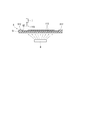
以上のようにして搬送トレイ5に収容された複数のデバイス113は、組立工程に搬送される。組立工程においては、図9に示すようにデバイス113毎にピップアップ装置のピックアップコレット7によってピックアップされるが、このとき搬送トレイ5を構成するトレイ本体51のデバイス支持部511およびタック層52が光透過性を有しているので、搬送トレイ5の下側から光源8によって光を照射することにより、個々のデバイス113を確実に認識することができる。即ち、個々のデバイス113は上述したように第1の分割予定ライン111および第2の分割予定ライン112に沿って切断された切断溝によって分割されているので、搬送トレイ5の下側から光を照射することにより、個々のデバイス113に分割した切断溝を通して光は通過するため、この通過した光に囲まれたデバイス113を確実に認識することができる。
The plurality of
1:パッケージ基板
113:デバイス
2:保持治具
20:吸引保持部
21、22:逃がし溝
23:吸引孔
3:切削装置
32:吸引テーブル
33:スピンドルユニット
333:切削ブレード
5:搬送トレイ
51:トレイ本体
511:デバイス支持部
512:枠部
52:タック層
6:デバイス搬送装置
61:吸引保持パッド
7:ピックアップコレット
1: Package substrate 113: Device 2: Holding jig 20:
Claims (2)
複数のデバイスを支持する表面を有するデバイス支持部と、該デバイス支持部の外周を囲繞して形成された枠部とを備えたトレイ本体と、
該トレイ本体のデバイス支持部の表面に装着されタック力を有するタック層と、を具備している、
ことを特徴とする搬送トレイ。 A transport tray that houses and transports a plurality of devices,
A tray body including a device support portion having a surface for supporting a plurality of devices, and a frame portion formed to surround the outer periphery of the device support portion;
A tack layer attached to the surface of the device support portion of the tray body and having tack force,
A transport tray characterized by that.
Priority Applications (3)
| Application Number | Priority Date | Filing Date | Title |
|---|---|---|---|
| JP2011002248A JP2012144261A (en) | 2011-01-07 | 2011-01-07 | Transport tray |
| TW100144830A TW201236954A (en) | 2011-01-07 | 2011-12-06 | Conveying tray |
| CN2012100021155A CN102582954A (en) | 2011-01-07 | 2012-01-05 | Transportation pallet |
Applications Claiming Priority (1)
| Application Number | Priority Date | Filing Date | Title |
|---|---|---|---|
| JP2011002248A JP2012144261A (en) | 2011-01-07 | 2011-01-07 | Transport tray |
Publications (1)
| Publication Number | Publication Date |
|---|---|
| JP2012144261A true JP2012144261A (en) | 2012-08-02 |
Family
ID=46472336
Family Applications (1)
| Application Number | Title | Priority Date | Filing Date |
|---|---|---|---|
| JP2011002248A Pending JP2012144261A (en) | 2011-01-07 | 2011-01-07 | Transport tray |
Country Status (3)
| Country | Link |
|---|---|
| JP (1) | JP2012144261A (en) |
| CN (1) | CN102582954A (en) |
| TW (1) | TW201236954A (en) |
Cited By (5)
| Publication number | Priority date | Publication date | Assignee | Title |
|---|---|---|---|---|
| JP2016201511A (en) * | 2015-04-14 | 2016-12-01 | 株式会社ディスコ | Carrying jig |
| JP2017117913A (en) * | 2015-12-24 | 2017-06-29 | 株式会社ディスコ | Chip housing tray |
| CN108792279A (en) * | 2018-06-26 | 2018-11-13 | 厦门市豪尔新材料股份有限公司 | A kind of protecting box and preparation method thereof, purposes |
| JP2020083392A (en) * | 2018-11-27 | 2020-06-04 | 日本電気硝子株式会社 | Tray, workpiece packaging body, and packaging method of workpiece |
| JP2022066967A (en) * | 2020-10-19 | 2022-05-02 | 株式会社ディスコ | Storage tray and manufacturing method of semiconductor chip package |
Families Citing this family (6)
| Publication number | Priority date | Publication date | Assignee | Title |
|---|---|---|---|---|
| CN104724336B (en) * | 2013-12-19 | 2017-01-04 | 福士瑞精密工业(晋城)有限公司 | Cutting agency |
| JP2017175055A (en) * | 2016-03-25 | 2017-09-28 | 株式会社ディスコ | Handling method for package wafer |
| TWI579220B (en) * | 2016-06-15 | 2017-04-21 | All Ring Tech Co Ltd | Method and device for component extraction of fitting process |
| TWI567008B (en) * | 2016-06-15 | 2017-01-21 | All Ring Tech Co Ltd | Assembly of the components of the transfer device |
| TWI574901B (en) * | 2016-06-15 | 2017-03-21 | All Ring Tech Co Ltd | Method and device for fitting method of fitting process |
| CN113212943B (en) * | 2021-07-07 | 2021-09-07 | 杭州硅土科技有限公司 | Self-cleaning vacuum release adsorption box for packaging precision devices and self-cleaning method |
Citations (5)
| Publication number | Priority date | Publication date | Assignee | Title |
|---|---|---|---|---|
| JP2001298080A (en) * | 2000-04-12 | 2001-10-26 | Oki Electric Ind Co Ltd | Chip tray |
| JP2008091696A (en) * | 2006-10-03 | 2008-04-17 | Seiko Instruments Inc | Semiconductor chip tray |
| JP2009023725A (en) * | 2007-07-24 | 2009-02-05 | Shin Etsu Polymer Co Ltd | Component holder |
| JP2010195413A (en) * | 2009-02-24 | 2010-09-09 | Shin Etsu Polymer Co Ltd | Holding tray, printing jig and printing method |
| JP2010222021A (en) * | 2009-03-23 | 2010-10-07 | Shin Etsu Polymer Co Ltd | Adhesive holding tray |
Family Cites Families (4)
| Publication number | Priority date | Publication date | Assignee | Title |
|---|---|---|---|---|
| JPH0824232B2 (en) * | 1989-05-29 | 1996-03-06 | ローム株式会社 | Chip parts front / back judgment device |
| JPH05193684A (en) * | 1992-01-08 | 1993-08-03 | Nec Kyushu Ltd | Semiconductor element transporting container |
| CN100470767C (en) * | 2004-03-26 | 2009-03-18 | 富士胶片株式会社 | Apparatus and method for bonding substrates |
| JP2008109015A (en) * | 2006-10-27 | 2008-05-08 | Disco Abrasive Syst Ltd | Wafer dividing method and dividing apparatus |
-
2011
- 2011-01-07 JP JP2011002248A patent/JP2012144261A/en active Pending
- 2011-12-06 TW TW100144830A patent/TW201236954A/en unknown
-
2012
- 2012-01-05 CN CN2012100021155A patent/CN102582954A/en active Pending
Patent Citations (5)
| Publication number | Priority date | Publication date | Assignee | Title |
|---|---|---|---|---|
| JP2001298080A (en) * | 2000-04-12 | 2001-10-26 | Oki Electric Ind Co Ltd | Chip tray |
| JP2008091696A (en) * | 2006-10-03 | 2008-04-17 | Seiko Instruments Inc | Semiconductor chip tray |
| JP2009023725A (en) * | 2007-07-24 | 2009-02-05 | Shin Etsu Polymer Co Ltd | Component holder |
| JP2010195413A (en) * | 2009-02-24 | 2010-09-09 | Shin Etsu Polymer Co Ltd | Holding tray, printing jig and printing method |
| JP2010222021A (en) * | 2009-03-23 | 2010-10-07 | Shin Etsu Polymer Co Ltd | Adhesive holding tray |
Cited By (9)
| Publication number | Priority date | Publication date | Assignee | Title |
|---|---|---|---|---|
| JP2016201511A (en) * | 2015-04-14 | 2016-12-01 | 株式会社ディスコ | Carrying jig |
| JP2017117913A (en) * | 2015-12-24 | 2017-06-29 | 株式会社ディスコ | Chip housing tray |
| KR20170076562A (en) * | 2015-12-24 | 2017-07-04 | 가부시기가이샤 디스코 | Chip storage tray |
| KR102465718B1 (en) * | 2015-12-24 | 2022-11-09 | 가부시기가이샤 디스코 | Method for picking up individually divided chips from chip storage tray |
| CN108792279A (en) * | 2018-06-26 | 2018-11-13 | 厦门市豪尔新材料股份有限公司 | A kind of protecting box and preparation method thereof, purposes |
| JP2020083392A (en) * | 2018-11-27 | 2020-06-04 | 日本電気硝子株式会社 | Tray, workpiece packaging body, and packaging method of workpiece |
| JP7183731B2 (en) | 2018-11-27 | 2022-12-06 | 日本電気硝子株式会社 | Tray, work package, and work packing method |
| JP2022066967A (en) * | 2020-10-19 | 2022-05-02 | 株式会社ディスコ | Storage tray and manufacturing method of semiconductor chip package |
| JP7601595B2 (en) | 2020-10-19 | 2024-12-17 | 株式会社ディスコ | Storage tray and method for manufacturing semiconductor chip package |
Also Published As
| Publication number | Publication date |
|---|---|
| CN102582954A (en) | 2012-07-18 |
| TW201236954A (en) | 2012-09-16 |
Similar Documents
| Publication | Publication Date | Title |
|---|---|---|
| JP2012144261A (en) | Transport tray | |
| JP5960532B2 (en) | Processing method of package substrate | |
| JP6605946B2 (en) | Method for picking up chips from the chip storage tray | |
| US10297488B2 (en) | Workpiece support jig | |
| JP2013065603A (en) | Dividing apparatus | |
| JP6301147B2 (en) | Holding jig | |
| JP2014175602A (en) | Holding jig | |
| TW201810398A (en) | Wafer processing system | |
| CN107017188A (en) | Split the dividing method of tool and chip | |
| JP4846411B2 (en) | Semiconductor package jig | |
| JP5373496B2 (en) | Cutting groove detecting device and cutting machine | |
| JP2012227485A (en) | Processing method of package substrate | |
| JP2014038947A (en) | Conveyance tray | |
| KR20170113189A (en) | Handling method of a package substrate | |
| JP2017199863A (en) | cassette | |
| JP4676288B2 (en) | Cutting equipment | |
| JP2010271616A (en) | Optical waveguide sheet cutting method and cutting apparatus | |
| JP2013222835A (en) | Method for dividing package substrate and dividing device | |
| KR102759843B1 (en) | Processing apparatus | |
| JP6475085B2 (en) | Chip unloading method | |
| JP2016201511A (en) | Carrying jig | |
| JP2019004069A (en) | Processing equipment | |
| JP2024125834A (en) | Processing Equipment | |
| JP2016137531A (en) | Chuck table | |
| JP2011077284A (en) | Cutting device |
Legal Events
| Date | Code | Title | Description |
|---|---|---|---|
| A621 | Written request for application examination |
Free format text: JAPANESE INTERMEDIATE CODE: A621 Effective date: 20131205 |
|
| A977 | Report on retrieval |
Free format text: JAPANESE INTERMEDIATE CODE: A971007 Effective date: 20140717 |
|
| A131 | Notification of reasons for refusal |
Free format text: JAPANESE INTERMEDIATE CODE: A131 Effective date: 20140819 |
|
| A521 | Written amendment |
Free format text: JAPANESE INTERMEDIATE CODE: A523 Effective date: 20141017 |
|
| A02 | Decision of refusal |
Free format text: JAPANESE INTERMEDIATE CODE: A02 Effective date: 20150421 |