JP2012137728A - Infrared transmission filter and imaging apparatus using the same - Google Patents
Infrared transmission filter and imaging apparatus using the same Download PDFInfo
- Publication number
- JP2012137728A JP2012137728A JP2011163519A JP2011163519A JP2012137728A JP 2012137728 A JP2012137728 A JP 2012137728A JP 2011163519 A JP2011163519 A JP 2011163519A JP 2011163519 A JP2011163519 A JP 2011163519A JP 2012137728 A JP2012137728 A JP 2012137728A
- Authority
- JP
- Japan
- Prior art keywords
- infrared light
- infrared
- light
- film
- wavelength
- Prior art date
- Legal status (The legal status is an assumption and is not a legal conclusion. Google has not performed a legal analysis and makes no representation as to the accuracy of the status listed.)
- Granted
Links
- 230000005540 biological transmission Effects 0.000 title claims abstract description 104
- 238000003384 imaging method Methods 0.000 title claims abstract description 10
- 230000031700 light absorption Effects 0.000 claims abstract description 64
- 239000000463 material Substances 0.000 claims abstract description 48
- 239000000758 substrate Substances 0.000 claims description 88
- 238000002834 transmittance Methods 0.000 claims description 66
- 239000006096 absorbing agent Substances 0.000 claims description 63
- 230000003595 spectral effect Effects 0.000 claims description 29
- 230000008859 change Effects 0.000 claims description 9
- 239000012528 membrane Substances 0.000 claims description 4
- 239000012780 transparent material Substances 0.000 claims description 2
- 230000002745 absorbent Effects 0.000 abstract description 2
- 239000002250 absorbent Substances 0.000 abstract description 2
- 239000010408 film Substances 0.000 description 206
- 239000010410 layer Substances 0.000 description 39
- 239000011521 glass Substances 0.000 description 37
- 229920005989 resin Polymers 0.000 description 28
- 239000011347 resin Substances 0.000 description 28
- VYPSYNLAJGMNEJ-UHFFFAOYSA-N Silicium dioxide Chemical compound O=[Si]=O VYPSYNLAJGMNEJ-UHFFFAOYSA-N 0.000 description 19
- GWEVSGVZZGPLCZ-UHFFFAOYSA-N Titan oxide Chemical compound O=[Ti]=O GWEVSGVZZGPLCZ-UHFFFAOYSA-N 0.000 description 18
- 238000000576 coating method Methods 0.000 description 14
- 238000000034 method Methods 0.000 description 14
- 239000000853 adhesive Substances 0.000 description 13
- 230000001070 adhesive effect Effects 0.000 description 13
- 230000000694 effects Effects 0.000 description 13
- 229920001225 polyester resin Polymers 0.000 description 10
- 239000004645 polyester resin Substances 0.000 description 10
- 239000011248 coating agent Substances 0.000 description 9
- 239000000377 silicon dioxide Substances 0.000 description 9
- 238000004544 sputter deposition Methods 0.000 description 8
- 238000001771 vacuum deposition Methods 0.000 description 8
- 238000010521 absorption reaction Methods 0.000 description 7
- 238000001035 drying Methods 0.000 description 7
- 230000035699 permeability Effects 0.000 description 7
- 239000000654 additive Substances 0.000 description 6
- JHIVVAPYMSGYDF-UHFFFAOYSA-N cyclohexanone Chemical compound O=C1CCCCC1 JHIVVAPYMSGYDF-UHFFFAOYSA-N 0.000 description 6
- 239000007788 liquid Substances 0.000 description 6
- -1 allyl ester Chemical class 0.000 description 5
- 239000002270 dispersing agent Substances 0.000 description 5
- 238000010438 heat treatment Methods 0.000 description 5
- RTZKZFJDLAIYFH-UHFFFAOYSA-N Diethyl ether Chemical compound CCOCC RTZKZFJDLAIYFH-UHFFFAOYSA-N 0.000 description 4
- 229910004298 SiO 2 Inorganic materials 0.000 description 4
- 229910010413 TiO 2 Inorganic materials 0.000 description 4
- MCMNRKCIXSYSNV-UHFFFAOYSA-N Zirconium dioxide Chemical compound O=[Zr]=O MCMNRKCIXSYSNV-UHFFFAOYSA-N 0.000 description 4
- 239000003963 antioxidant agent Substances 0.000 description 4
- 239000003795 chemical substances by application Substances 0.000 description 4
- 230000000052 comparative effect Effects 0.000 description 4
- 230000001771 impaired effect Effects 0.000 description 4
- 230000004048 modification Effects 0.000 description 4
- 238000012986 modification Methods 0.000 description 4
- 239000012788 optical film Substances 0.000 description 4
- 238000005268 plasma chemical vapour deposition Methods 0.000 description 4
- 229920000297 Rayon Polymers 0.000 description 3
- NIXOWILDQLNWCW-UHFFFAOYSA-N acrylic acid group Chemical group C(C=C)(=O)O NIXOWILDQLNWCW-UHFFFAOYSA-N 0.000 description 3
- 239000002518 antifoaming agent Substances 0.000 description 3
- 239000002216 antistatic agent Substances 0.000 description 3
- 230000015572 biosynthetic process Effects 0.000 description 3
- 239000007822 coupling agent Substances 0.000 description 3
- 239000002612 dispersion medium Substances 0.000 description 3
- 239000003063 flame retardant Substances 0.000 description 3
- 239000000314 lubricant Substances 0.000 description 3
- 238000004519 manufacturing process Methods 0.000 description 3
- 229910052751 metal Inorganic materials 0.000 description 3
- 239000002184 metal Substances 0.000 description 3
- 230000003287 optical effect Effects 0.000 description 3
- BPUBBGLMJRNUCC-UHFFFAOYSA-N oxygen(2-);tantalum(5+) Chemical compound [O-2].[O-2].[O-2].[O-2].[O-2].[Ta+5].[Ta+5] BPUBBGLMJRNUCC-UHFFFAOYSA-N 0.000 description 3
- 239000011342 resin composition Substances 0.000 description 3
- 239000002904 solvent Substances 0.000 description 3
- 238000003756 stirring Methods 0.000 description 3
- 239000003017 thermal stabilizer Substances 0.000 description 3
- 239000004925 Acrylic resin Substances 0.000 description 2
- 229920000178 Acrylic resin Polymers 0.000 description 2
- PPBRXRYQALVLMV-UHFFFAOYSA-N Styrene Chemical compound C=CC1=CC=CC=C1 PPBRXRYQALVLMV-UHFFFAOYSA-N 0.000 description 2
- XLOMVQKBTHCTTD-UHFFFAOYSA-N Zinc monoxide Chemical compound [Zn]=O XLOMVQKBTHCTTD-UHFFFAOYSA-N 0.000 description 2
- PNEYBMLMFCGWSK-UHFFFAOYSA-N aluminium oxide Inorganic materials [O-2].[O-2].[O-2].[Al+3].[Al+3] PNEYBMLMFCGWSK-UHFFFAOYSA-N 0.000 description 2
- 230000003078 antioxidant effect Effects 0.000 description 2
- 238000007611 bar coating method Methods 0.000 description 2
- 239000011324 bead Substances 0.000 description 2
- 230000008901 benefit Effects 0.000 description 2
- 238000004891 communication Methods 0.000 description 2
- 239000003989 dielectric material Substances 0.000 description 2
- 229910001385 heavy metal Inorganic materials 0.000 description 2
- 238000010030 laminating Methods 0.000 description 2
- MRELNEQAGSRDBK-UHFFFAOYSA-N lanthanum(3+);oxygen(2-) Chemical compound [O-2].[O-2].[O-2].[La+3].[La+3] MRELNEQAGSRDBK-UHFFFAOYSA-N 0.000 description 2
- ORUIBWPALBXDOA-UHFFFAOYSA-L magnesium fluoride Chemical compound [F-].[F-].[Mg+2] ORUIBWPALBXDOA-UHFFFAOYSA-L 0.000 description 2
- 229910001635 magnesium fluoride Inorganic materials 0.000 description 2
- 150000002739 metals Chemical class 0.000 description 2
- IEQIEDJGQAUEQZ-UHFFFAOYSA-N phthalocyanine Chemical class N1C(N=C2C3=CC=CC=C3C(N=C3C4=CC=CC=C4C(=N4)N3)=N2)=C(C=CC=C2)C2=C1N=C1C2=CC=CC=C2C4=N1 IEQIEDJGQAUEQZ-UHFFFAOYSA-N 0.000 description 2
- 239000000049 pigment Substances 0.000 description 2
- 239000004014 plasticizer Substances 0.000 description 2
- 229920005668 polycarbonate resin Polymers 0.000 description 2
- 239000004431 polycarbonate resin Substances 0.000 description 2
- 229920001721 polyimide Polymers 0.000 description 2
- 239000004065 semiconductor Substances 0.000 description 2
- 230000035945 sensitivity Effects 0.000 description 2
- 239000002356 single layer Substances 0.000 description 2
- PBCFLUZVCVVTBY-UHFFFAOYSA-N tantalum pentoxide Inorganic materials O=[Ta](=O)O[Ta](=O)=O PBCFLUZVCVVTBY-UHFFFAOYSA-N 0.000 description 2
- 150000003573 thiols Chemical class 0.000 description 2
- 239000006097 ultraviolet radiation absorber Substances 0.000 description 2
- QGKMIGUHVLGJBR-UHFFFAOYSA-M (4z)-1-(3-methylbutyl)-4-[[1-(3-methylbutyl)quinolin-1-ium-4-yl]methylidene]quinoline;iodide Chemical class [I-].C12=CC=CC=C2N(CCC(C)C)C=CC1=CC1=CC=[N+](CCC(C)C)C2=CC=CC=C12 QGKMIGUHVLGJBR-UHFFFAOYSA-M 0.000 description 1
- ZXDDPOHVAMWLBH-UHFFFAOYSA-N 2,4-Dihydroxybenzophenone Chemical compound OC1=CC(O)=CC=C1C(=O)C1=CC=CC=C1 ZXDDPOHVAMWLBH-UHFFFAOYSA-N 0.000 description 1
- ROHFBIREHKPELA-UHFFFAOYSA-N 2-[(3,5-ditert-butyl-4-hydroxyphenyl)methyl]prop-2-enoic acid;methane Chemical compound C.CC(C)(C)C1=CC(CC(=C)C(O)=O)=CC(C(C)(C)C)=C1O.CC(C)(C)C1=CC(CC(=C)C(O)=O)=CC(C(C)(C)C)=C1O.CC(C)(C)C1=CC(CC(=C)C(O)=O)=CC(C(C)(C)C)=C1O.CC(C)(C)C1=CC(CC(=C)C(O)=O)=CC(C(C)(C)C)=C1O ROHFBIREHKPELA-UHFFFAOYSA-N 0.000 description 1
- QTBSBXVTEAMEQO-UHFFFAOYSA-M Acetate Chemical compound CC([O-])=O QTBSBXVTEAMEQO-UHFFFAOYSA-M 0.000 description 1
- NLZUEZXRPGMBCV-UHFFFAOYSA-N Butylhydroxytoluene Chemical compound CC1=CC(C(C)(C)C)=C(O)C(C(C)(C)C)=C1 NLZUEZXRPGMBCV-UHFFFAOYSA-N 0.000 description 1
- 239000004215 Carbon black (E152) Substances 0.000 description 1
- 239000004593 Epoxy Substances 0.000 description 1
- LFQSCWFLJHTTHZ-UHFFFAOYSA-N Ethanol Chemical compound CCO LFQSCWFLJHTTHZ-UHFFFAOYSA-N 0.000 description 1
- 239000004962 Polyamide-imide Substances 0.000 description 1
- 239000004642 Polyimide Substances 0.000 description 1
- RTAQQCXQSZGOHL-UHFFFAOYSA-N Titanium Chemical compound [Ti] RTAQQCXQSZGOHL-UHFFFAOYSA-N 0.000 description 1
- 229920001807 Urea-formaldehyde Polymers 0.000 description 1
- 239000005083 Zinc sulfide Substances 0.000 description 1
- RUFZJUYWZZUTJE-UHFFFAOYSA-J [F-].[F-].[F-].[F-].F.F.[Na+].[Al+3] Chemical compound [F-].[F-].[F-].[F-].F.F.[Na+].[Al+3] RUFZJUYWZZUTJE-UHFFFAOYSA-J 0.000 description 1
- 229920000122 acrylonitrile butadiene styrene Polymers 0.000 description 1
- 150000001299 aldehydes Chemical class 0.000 description 1
- 150000001338 aliphatic hydrocarbons Chemical class 0.000 description 1
- 229910052782 aluminium Inorganic materials 0.000 description 1
- XAGFODPZIPBFFR-UHFFFAOYSA-N aluminium Chemical compound [Al] XAGFODPZIPBFFR-UHFFFAOYSA-N 0.000 description 1
- 150000001412 amines Chemical class 0.000 description 1
- PYKYMHQGRFAEBM-UHFFFAOYSA-N anthraquinone Natural products CCC(=O)c1c(O)c2C(=O)C3C(C=CC=C3O)C(=O)c2cc1CC(=O)OC PYKYMHQGRFAEBM-UHFFFAOYSA-N 0.000 description 1
- 150000004945 aromatic hydrocarbons Chemical class 0.000 description 1
- 125000000751 azo group Chemical group [*]N=N[*] 0.000 description 1
- 230000000903 blocking effect Effects 0.000 description 1
- 229910052793 cadmium Inorganic materials 0.000 description 1
- BDOSMKKIYDKNTQ-UHFFFAOYSA-N cadmium atom Chemical compound [Cd] BDOSMKKIYDKNTQ-UHFFFAOYSA-N 0.000 description 1
- 238000005266 casting Methods 0.000 description 1
- 239000012461 cellulose resin Substances 0.000 description 1
- 150000001875 compounds Chemical class 0.000 description 1
- 238000007766 curtain coating Methods 0.000 description 1
- 238000005520 cutting process Methods 0.000 description 1
- 230000007423 decrease Effects 0.000 description 1
- 230000006866 deterioration Effects 0.000 description 1
- 150000008049 diazo compounds Chemical class 0.000 description 1
- 238000007607 die coating method Methods 0.000 description 1
- 238000003618 dip coating Methods 0.000 description 1
- 239000003822 epoxy resin Substances 0.000 description 1
- 150000002148 esters Chemical class 0.000 description 1
- 238000007756 gravure coating Methods 0.000 description 1
- LNEPOXFFQSENCJ-UHFFFAOYSA-N haloperidol Chemical compound C1CC(O)(C=2C=CC(Cl)=CC=2)CCN1CCCC(=O)C1=CC=C(F)C=C1 LNEPOXFFQSENCJ-UHFFFAOYSA-N 0.000 description 1
- 229930195733 hydrocarbon Natural products 0.000 description 1
- 230000006872 improvement Effects 0.000 description 1
- 230000001678 irradiating effect Effects 0.000 description 1
- 150000002576 ketones Chemical class 0.000 description 1
- 238000003475 lamination Methods 0.000 description 1
- 150000002734 metacrylic acid derivatives Chemical class 0.000 description 1
- 238000002156 mixing Methods 0.000 description 1
- 239000000203 mixture Substances 0.000 description 1
- 238000000465 moulding Methods 0.000 description 1
- LKKPNUDVOYAOBB-UHFFFAOYSA-N naphthalocyanine Chemical class N1C(N=C2C3=CC4=CC=CC=C4C=C3C(N=C3C4=CC5=CC=CC=C5C=C4C(=N4)N3)=N2)=C(C=C2C(C=CC=C2)=C2)C2=C1N=C1C2=CC3=CC=CC=C3C=C2C4=N1 LKKPNUDVOYAOBB-UHFFFAOYSA-N 0.000 description 1
- ZKATWMILCYLAPD-UHFFFAOYSA-N niobium pentoxide Inorganic materials O=[Nb](=O)O[Nb](=O)=O ZKATWMILCYLAPD-UHFFFAOYSA-N 0.000 description 1
- URLJKFSTXLNXLG-UHFFFAOYSA-N niobium(5+);oxygen(2-) Chemical compound [O-2].[O-2].[O-2].[O-2].[O-2].[Nb+5].[Nb+5] URLJKFSTXLNXLG-UHFFFAOYSA-N 0.000 description 1
- DXGLGDHPHMLXJC-UHFFFAOYSA-N oxybenzone Chemical compound OC1=CC(OC)=CC=C1C(=O)C1=CC=CC=C1 DXGLGDHPHMLXJC-UHFFFAOYSA-N 0.000 description 1
- DOIRQSBPFJWKBE-UHFFFAOYSA-N phthalic acid di-n-butyl ester Natural products CCCCOC(=O)C1=CC=CC=C1C(=O)OCCCC DOIRQSBPFJWKBE-UHFFFAOYSA-N 0.000 description 1
- 239000004033 plastic Substances 0.000 description 1
- 229920003023 plastic Polymers 0.000 description 1
- 229920006122 polyamide resin Polymers 0.000 description 1
- 229920002312 polyamide-imide Polymers 0.000 description 1
- 229920000647 polyepoxide Polymers 0.000 description 1
- 239000009719 polyimide resin Substances 0.000 description 1
- 229920005672 polyolefin resin Polymers 0.000 description 1
- 229920001296 polysiloxane Polymers 0.000 description 1
- 229920000915 polyvinyl chloride Polymers 0.000 description 1
- 239000004800 polyvinyl chloride Substances 0.000 description 1
- 238000002360 preparation method Methods 0.000 description 1
- 230000002265 prevention Effects 0.000 description 1
- 230000009467 reduction Effects 0.000 description 1
- 238000007761 roller coating Methods 0.000 description 1
- 229910000077 silane Inorganic materials 0.000 description 1
- 229920002050 silicone resin Polymers 0.000 description 1
- 238000004528 spin coating Methods 0.000 description 1
- 238000005507 spraying Methods 0.000 description 1
- 239000004094 surface-active agent Substances 0.000 description 1
- 229920003002 synthetic resin Polymers 0.000 description 1
- 239000000057 synthetic resin Substances 0.000 description 1
- 229910001936 tantalum oxide Inorganic materials 0.000 description 1
- 229920002803 thermoplastic polyurethane Polymers 0.000 description 1
- BYMUNNMMXKDFEZ-UHFFFAOYSA-K trifluorolanthanum Chemical compound F[La](F)F BYMUNNMMXKDFEZ-UHFFFAOYSA-K 0.000 description 1
- XLYOFNOQVPJJNP-UHFFFAOYSA-N water Substances O XLYOFNOQVPJJNP-UHFFFAOYSA-N 0.000 description 1
- 239000013585 weight reducing agent Substances 0.000 description 1
- RUDFQVOCFDJEEF-UHFFFAOYSA-N yttrium(III) oxide Inorganic materials [O-2].[O-2].[O-2].[Y+3].[Y+3] RUDFQVOCFDJEEF-UHFFFAOYSA-N 0.000 description 1
- 239000011787 zinc oxide Substances 0.000 description 1
- 229910052984 zinc sulfide Inorganic materials 0.000 description 1
- DRDVZXDWVBGGMH-UHFFFAOYSA-N zinc;sulfide Chemical compound [S-2].[Zn+2] DRDVZXDWVBGGMH-UHFFFAOYSA-N 0.000 description 1
Images


Classifications
-
- H—ELECTRICITY
- H01—ELECTRIC ELEMENTS
- H01L—SEMICONDUCTOR DEVICES NOT COVERED BY CLASS H10
- H01L27/00—Devices consisting of a plurality of semiconductor or other solid-state components formed in or on a common substrate
- H01L27/14—Devices consisting of a plurality of semiconductor or other solid-state components formed in or on a common substrate including semiconductor components sensitive to infrared radiation, light, electromagnetic radiation of shorter wavelength or corpuscular radiation and specially adapted either for the conversion of the energy of such radiation into electrical energy or for the control of electrical energy by such radiation
- H01L27/144—Devices controlled by radiation
- H01L27/146—Imager structures
- H01L27/14601—Structural or functional details thereof
- H01L27/1462—Coatings
- H01L27/14621—Colour filter arrangements
-
- G—PHYSICS
- G02—OPTICS
- G02B—OPTICAL ELEMENTS, SYSTEMS OR APPARATUS
- G02B5/00—Optical elements other than lenses
- G02B5/20—Filters
- G02B5/208—Filters for use with infrared or ultraviolet radiation, e.g. for separating visible light from infrared and/or ultraviolet radiation
-
- G—PHYSICS
- G02—OPTICS
- G02B—OPTICAL ELEMENTS, SYSTEMS OR APPARATUS
- G02B5/00—Optical elements other than lenses
- G02B5/20—Filters
- G02B5/22—Absorbing filters
Abstract
Description
本発明は、赤外光透過フィルタ、及びこれを用いた赤外線カメラ等の撮像装置に関する。 The present invention relates to an infrared light transmission filter and an imaging device such as an infrared camera using the same.
近年、テレビ、オーディオ、エアコン等の家電製品の赤外線リモコンを始め、携帯電話やパーソナルコンピューター間の情報のやり取りを行う赤外線通信、夜間の撮影や防犯用途などに使用する赤外線カメラ、人感センサー等、特定の赤外波長領域(0.7μm〜2.5μm)の光(以下、赤外光ともいう)を利用する機器が増大し、それに伴い、これらの機器ではノイズとなる可視波長領域の光(以下、可視光ともいう)を遮光し、赤外光のみを選択的に透過させるフィルタの需要が高まっている。さらに赤外線カメラには入射角度が約0±40°といった広範囲な視野角が求められている。 In recent years, infrared remote control for home appliances such as TV, audio, air conditioner, infrared communication for exchanging information between mobile phones and personal computers, infrared cameras used for night shooting and crime prevention applications, human sensor, etc. With the increase in devices that use light in a specific infrared wavelength region (0.7 μm to 2.5 μm) (hereinafter also referred to as infrared light), in these devices, light in the visible wavelength region that causes noise ( Hereinafter, there is an increasing demand for a filter that shields visible light) and selectively transmits only infrared light. In addition, infrared cameras are required to have a wide viewing angle with an incident angle of about 0 ± 40 °.
従来、上記赤外光透過フィルタとしては、例えば、ガラス基材の表面に誘電体からなる多層膜を蒸着して可視光を反射するようにしたもの、ガラスにカドミウム(Cd)等の金属をドープして可視光を吸収するようにしたもの、さらには、アクリル樹脂、ポリカーボネート樹脂などの透明樹脂に可視光を吸収する色素を含有させたもの等が知られている(例えば、特許文献1、2参照)。
Conventionally, as the infrared light transmitting filter, for example, a multilayer film made of a dielectric is deposited on the surface of a glass substrate to reflect visible light, and glass is doped with a metal such as cadmium (Cd). In which visible light is absorbed, and further, a transparent resin such as an acrylic resin or a polycarbonate resin containing a pigment that absorbs visible light is known (for example,
しかしながら、ガラス基材に誘電体多層膜を蒸着した反射型のフィルタは、可視光の入射角度により遮光(カットオフ)特性が変化するという入射角依存性の問題があった。また、金属をドープした可視光吸収型のガラスフィルタは、ドープする金属としてCd等の重金属が使用されるため最近は敬遠される傾向にある。また、質量が大きく、かつ薄型化が困難であるために、カメラ等の小型軽量化が要求される用途に用いるのは適当ではなかった。さらに価格が高いという問題もあった。 However, the reflection type filter in which the dielectric multilayer film is vapor-deposited on the glass substrate has a problem of the incident angle dependency that the light shielding (cutoff) characteristic changes depending on the incident angle of visible light. In addition, visible light absorption type glass filters doped with metals tend to be avoided recently because heavy metals such as Cd are used as doping metals. Further, since the mass is large and it is difficult to reduce the thickness, it is not suitable for use in applications that require a reduction in size and weight, such as a camera. There was also the problem of high prices.
一方、透明樹脂に色素を含有させた有機フィルタは、軽量で薄型化が可能であり、反射型フィルタのような入射角依存性等の問題もない。しかしながら、従来のこの種のフィルタは、可視光寄りの赤外光の選択透過性が必ずしも十分ではなかった。具体的には、730〜830nmの波長領域の光に対する遮光特性に乏しかった。このため、例えば、波長830〜850nmの光を被写体に照射し、その反射光を赤外線カメラで撮像するような用途では、S/N比が小さくなってしまうことから、実用に供することはできなかった。 On the other hand, an organic filter in which a pigment is contained in a transparent resin is lightweight and can be thinned, and does not have problems such as incident angle dependency as in a reflective filter. However, this type of conventional filter does not always have sufficient selective transmission of infrared light close to visible light. Specifically, the light shielding properties with respect to light in the wavelength region of 730 to 830 nm were poor. For this reason, for example, in an application where a subject is irradiated with light having a wavelength of 830 to 850 nm and the reflected light is imaged with an infrared camera, the S / N ratio becomes small, so that it cannot be put to practical use. It was.
本発明は、安価で、十分な軽量化、薄型化を達成でき、また反射型フィルタのような入射角依存性の問題がなく、かつ赤外光の選択透過性に優れる(透過率が急峻に変化する)赤外光透過フィルタ、及びそのような赤外光透過フィルタを用いた光学特性に優れる撮像装置の提供を目的とする。 The present invention is inexpensive, can be sufficiently lightened and thinned, has no problem of incident angle dependency like a reflective filter, and has excellent selective transmission of infrared light (has a sharp transmittance). It is an object of the present invention to provide an infrared transmission filter that changes) and an imaging device that has excellent optical characteristics using such an infrared transmission filter.
本発明の一態様に係る赤外光透過フィルタは、赤外波長領域の光を選択的に透過する赤外光透過性基材と、その一方の面上に形成された、前記赤外光透過性基材の透過波長帯域の短波長側に光吸収端を有する近赤外線吸収剤を含む短波長側赤外光吸収膜(以下、(短)赤外光吸収膜ともいう)と、を具備することを特徴としている。 An infrared light transmission filter according to one embodiment of the present invention includes an infrared light transmission base material that selectively transmits light in an infrared wavelength region, and the infrared light transmission filter formed on one surface thereof. A short wavelength side infrared light absorption film (hereinafter also referred to as a (short) infrared light absorption film) including a near infrared absorber having a light absorption edge on the short wavelength side of the transmission wavelength band of the conductive substrate. It is characterized by that.
上記赤外光透過フィルタにおいて、前記近赤外線吸収剤の光吸収端の波長が730〜830nmであってよい。なお、(短)赤外光吸収膜を備えるにあたり400〜1100nmにおける波長領域において、(短)赤外光吸収膜の分光透過率の最も低くなる点が、0〜1%となるように(短)赤外光吸収膜の膜厚及び近赤外線吸収剤の濃度を調整することが好ましい。本明細書における「光吸収端の波長」とは、この分光透過率が1%以下となる波長のことをいう。 In the infrared light transmission filter, a wavelength of a light absorption edge of the near infrared absorber may be 730 to 830 nm. When the (short) infrared light absorbing film is provided, the spectral transmittance of the (short) infrared light absorbing film is lowest in the wavelength region of 400 to 1100 nm so that it is 0 to 1% (short). ) It is preferable to adjust the film thickness of the infrared light absorbing film and the concentration of the near infrared absorbing agent. The “wavelength at the light absorption edge” in this specification means a wavelength at which the spectral transmittance is 1% or less.
上記赤外光透過フィルタにおいて、前記赤外光透過性基材が、可視波長領域の光を吸収する可視光吸収剤を含む透明材料からなってもよい。 In the infrared light transmitting filter, the infrared light transmitting base material may be made of a transparent material including a visible light absorber that absorbs light in a visible wavelength region.
上記赤外光透過フィルタにおいて、前記赤外光透過性基材が、透明基材と、その一方の面上に形成された可視波長領域の光を吸収する可視光吸収剤を含む可視光吸収膜を備えていてもよい。 In the infrared light transmitting filter, the infrared light transmitting base material includes a transparent base material and a visible light absorbing film including a visible light absorber that absorbs light in a visible wavelength region formed on one surface of the transparent base material. May be provided.
上記赤外光透過フィルタにおいて、前記赤外光透過性基材が、透明基材と、その一方の面上に形成された可視波長領域の光を反射する誘電体多層膜からなる可視光反射膜を備えてなり、前記透明基材の他方の面側に前記(短)赤外光吸収膜が形成されていてもよい。 In the infrared light transmitting filter, the infrared light transmitting base material is a visible light reflecting film comprising a transparent base material and a dielectric multilayer film that reflects light in a visible wavelength region formed on one surface thereof. The (short) infrared light absorbing film may be formed on the other surface side of the transparent substrate.
上記赤外光透過フィルタにおいて、前記赤外光透過性基材の透過波長帯域の長波長側の光を反射する誘電体多層膜からなる長波長側赤外光反射膜(以下、(長)赤外光反射膜ともいう)をさらに備えていてもよい。 In the infrared light transmitting filter, a long wavelength side infrared light reflecting film (hereinafter referred to as (long) red) made of a dielectric multilayer film that reflects light on a long wavelength side of a transmission wavelength band of the infrared light transmitting base material. (Also referred to as an external light reflecting film).
垂直に入射する光に対する前記(長)赤外光反射膜の反射波長帯域が860〜1100nmであってもよい。 The reflection wavelength band of the (long) infrared light reflection film for vertically incident light may be 860 to 1100 nm.
上記赤外光透過フィルタにおいて、前記赤外光透過性基材の透過波長帯域の短波長側の光を反射する誘電体多層膜からなる短波長側赤外光反射膜(以下、(短)赤外光反射膜ともいう)をさらに備えていてもよい。 In the infrared light transmitting filter, a short wavelength infrared light reflecting film (hereinafter referred to as (short) red) composed of a dielectric multilayer film that reflects light on a short wavelength side of a transmission wavelength band of the infrared light transmitting substrate. (Also referred to as an external light reflecting film).
垂直に入射する光に対する前記(短)赤外光反射膜の反射波長帯域が700〜830nmであってもよい。 The reflection wavelength band of the (short) infrared light reflection film for vertically incident light may be 700 to 830 nm.
上記赤外光透過フィルタにおいて、下式で表わされる透過率の変化量D’が、1%/nm以上であってよい。
D’(%/nm)=[T810(%)−T760(%)]/[810(nm)−760(nm)]
(式中、T810は、分光透過率曲線における波長810nmの透過率であり、T760は、分光透過率曲線における波長760nmの透過率である)
In the infrared light transmission filter, the transmittance change amount D ′ represented by the following formula may be 1% / nm or more.
D ′ (% / nm) = [T 810 (%) − T 760 (%)] / [810 (nm) −760 (nm)]
(Where T 810 is the transmittance at a wavelength of 810 nm in the spectral transmittance curve, and T 760 is the transmittance at a wavelength of 760 nm in the spectral transmittance curve)
本発明の他の態様に係る撮像装置は、上記赤外光透過フィルタを備えたことを特徴としている。 An imaging apparatus according to another aspect of the present invention includes the infrared light transmission filter.
本発明によれば、安価で、十分な小型化、薄型化を達成でき、また反射型フィルタのような入射角依存性等の問題がなく、かつ十分に優れた赤外光選択透過性を有する赤外光透過フィルタが提供される。また、本発明によれば、そのような赤外光透過フィルタを備えた光学特性に優れる撮像装置が提供される。 According to the present invention, it is inexpensive, can be sufficiently reduced in size and thickness, has no problems such as incident angle dependency like a reflective filter, and has sufficiently excellent infrared light selective transmission. An infrared light transmission filter is provided. In addition, according to the present invention, there is provided an imaging device having such an infrared light transmission filter and excellent in optical characteristics.
以下、本発明の実施の形態について説明する。なお、以下では本発明の実施の形態を図面に基づいて説明するが、それらの図面は図解のために提供されるものであり、本発明はそれらの図面に何ら限定されない。 Embodiments of the present invention will be described below. In the following, embodiments of the present invention will be described with reference to the drawings. However, the drawings are provided for illustration, and the present invention is not limited to the drawings.
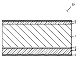
(第1の実施の形態)
図1は、本発明の第1の実施の形態による赤外光透過フィルタの一部を概略的に示す断面図である。図1に示すように、本実施形態の赤外光透過フィルタ10は、赤外光透過性基材1と、その一方の面に形成された、近赤外線吸収剤を含む(短)赤外光吸収膜2と、これらの両面に設けられた反射防止膜3とを備える。
(First embodiment)
FIG. 1 is a cross-sectional view schematically showing a part of an infrared light transmission filter according to a first embodiment of the present invention. As shown in FIG. 1, the infrared
赤外光透過性基材1は、可視波長領域の光を吸収する可視光吸収剤を含む透明樹脂から構成される。ここで、「透明樹脂」とは赤外波長領域の光を透過する合成樹脂をいう。透明樹脂としては、アクリル樹脂、スチレン樹脂、ABS樹脂、AS樹脂、ポリカーボネート樹脂、ポリオレフィン樹脂、ポリ塩化ビニル樹脂、アセテート系樹脂、セルロース系樹脂、ポリエステル樹脂、アリルエステル樹脂、ポリイミド樹脂、ポリアミド樹脂、ポリイミドエーテル樹脂、ポリアミドイミド樹脂、エポキシ樹脂、ウレタン樹脂、ウレア樹脂等が挙げられる。
The infrared light
また、可視波長領域の光を吸収する可視光吸収剤としては、フタロシアニン系化合物、アントラキノン系化合物、アゾ系化合物、ジアゾ系化合物等が挙げられる。可視光吸収剤は1種を単独で使用してもよく、2種以上を混合して用いてもよい。 Examples of the visible light absorber that absorbs light in the visible wavelength region include phthalocyanine compounds, anthraquinone compounds, azo compounds, and diazo compounds. A visible light absorber may be used individually by 1 type, and 2 or more types may be mixed and used for it.
赤外光透過性基材1における可視光吸収剤の含有量は、0.01〜10質量%が好ましい。可視光吸収剤の含有量が0.01質量%未満では、可視光を十分に吸収できないおそれがあり、また、10質量%を超えると、赤外光の透過性が低下するおそれがある。
The content of the visible light absorber in the infrared light
透明樹脂には、可視光吸収剤の他に、さらに、本発明の効果を阻害しない範囲で、紫外線吸収剤、酸化防止剤、レベリング剤、消泡剤、帯電防止剤、熱安定剤、分散剤、難燃剤、滑剤、可塑剤等の添加剤が含有されていてもよい。 In addition to the visible light absorber, the transparent resin further includes an ultraviolet absorber, an antioxidant, a leveling agent, an antifoaming agent, an antistatic agent, a thermal stabilizer, and a dispersing agent as long as the effects of the present invention are not impaired. Additives such as flame retardants, lubricants, and plasticizers may be contained.
紫外線吸収剤としては、例えば、2,4−ジヒドロキシベンゾフェノン、2−ヒドロキシ−4−メトキシベンゾフェノン等が挙げられる。酸化防止剤としては、例えば、2,6−ジ−t−ブチル−4−メチルフェノール、2,2’−ジオキシ−3,3’−ジ−−t−ブチル−5,5’−ジメチルジフェニルメタン、テトラキス[メチレン−3−(3,5−ジ−t−ブチル−4−ヒドロキシフェニル)プロピオネート]メタン等が挙げられる。 Examples of the ultraviolet absorber include 2,4-dihydroxybenzophenone and 2-hydroxy-4-methoxybenzophenone. Examples of the antioxidant include 2,6-di-t-butyl-4-methylphenol, 2,2′-dioxy-3,3′-di-t-butyl-5,5′-dimethyldiphenylmethane, And tetrakis [methylene-3- (3,5-di-t-butyl-4-hydroxyphenyl) propionate] methane.
赤外光透過性基材1は、例えば、透明樹脂、可視光吸収剤、及び必要に応じて配合される他の添加剤を、分散媒または溶媒に分散または溶解させて液状樹脂組成物を調製し、この液状樹脂組成物を剥離性の支持体上にキャスティングし、乾燥させた後、剥離性支持体から剥離することにより製造できる。赤外光透過性基材1は、また、透明樹脂、可視光吸収剤、及び必要に応じて配合される他の添加剤を混合して樹脂組成物を調製し、これを溶融成形することにより製造できる。
The infrared light
なお、可視光吸収剤を含む透明樹脂からなる赤外光透過性基材及びその材料となる可視光吸収剤を含む透明樹脂は市販されており、このような市販品から適宜選択して使用してもよい。例えば、板状の赤外光透過性基材として、三菱レイヨン(株)製のアクリフィルターIR75(商品名)等が挙げられる。また、ペレット状の透明樹脂として、(株)クラレ製のパラフィルター(商品名)等が挙げられる。 In addition, an infrared light transmissive substrate made of a transparent resin containing a visible light absorber and a transparent resin containing a visible light absorber as the material thereof are commercially available, and can be used by appropriately selecting from such commercially available products. May be. For example, an acrylic filter IR75 (trade name) manufactured by Mitsubishi Rayon Co., Ltd. may be used as the plate-like infrared light transmissive substrate. Moreover, as a pellet-shaped transparent resin, Kuraray Co., Ltd. para filter (brand name) etc. are mentioned.
赤外光透過性基材1の厚みは、特に限定されないが、軽量化、薄肉化を図る点からは、0.1〜3mmの範囲が好ましく、0.1〜1mmの範囲がより好ましい。
The thickness of the infrared light
近赤外線吸収剤を含む(短)赤外光吸収膜2は、近赤外線吸収剤を含む透明樹脂から構成される。透明樹脂としては、赤外光透過性基材1で用いたものと同様のものを使用できる。また、近赤外線吸収剤としては、赤外光透過性基材1の透過波長帯域の短波長側に光吸収端を有するもの、好ましくは光吸収端の波長が730〜830nmであるものが使用される。このような吸収特性を有する近赤外線吸収剤としては、例えば、フタロシアニン系化合物、ナフタロシアニン系化合物、シアニン系化合物、ジイモニウム系化合物、ジチオール金属錯体系化合物等が挙げられる。これらは1種を単独で使用してもよく、2種以上を混合して用いてもよい。近赤外線吸収剤の好ましい具体例としては、約760nmに光吸収端を有する山田化学工業(株)製のNIR−43V、QCR Solutions Corp.製のNIR757A(以上、商品名)等が挙げられる。
The (short) infrared
(短)赤外光吸収膜2における近赤外線吸収剤の含有量は、0.1〜10質量%が好ましく、0.5〜5質量%がより好ましい。近赤外線吸収剤の含有量が0.1質量%未満では、使用による効果が十分に得られないおそれがあり、また、10質量%を超えると、赤外波長領域の光の透過性が低下するおそれがある。
(Short) The content of the near infrared absorber in the infrared
(短)赤外光吸収膜2を構成する透明樹脂には、近赤外線吸収剤の他に、さらに、本発明の効果を阻害しない範囲で、赤外光透過性基材1で用いたものと同様の添加剤、例えば、紫外線吸収剤、酸化防止剤、レベリング剤、消泡剤、帯電防止剤、熱安定剤、分散剤、難燃剤、滑剤、可塑剤等が含有されていてもよい。
(Short) In addition to the near-infrared absorber, the transparent resin constituting the infrared-light-absorbing
近赤外線吸収剤を含む(短)赤外光吸収膜2は、近赤外線吸収剤、及び必要に応じて配合される他の添加剤を含む透明樹脂を、分散媒または溶媒に分散または溶解させて塗工液を調製し、この塗工液を上記赤外光透過性基材1の一方の面に塗工し、乾燥させることにより形成される。塗工、乾燥は、複数回に分けて行うことができる。
The (short) infrared
分散媒または溶媒としては、水、アルコール、ケトン、エーテル、エステル、アルデヒド、アミン、脂肪族炭化水素、脂環族炭化水素、芳香族炭化水素等が挙げられる。これらは、1種を単独で用いてもよく、2種以上を混合して用いてもよい。塗工液には、必要に応じて分散剤を配合できる。分散剤としては、例えば、界面活性剤、シラン化合物、シリコーンレジン、チタネート系カップリング剤、アルミニウム系カップリング剤、ジルコアルミネート系カップリング剤等が使用される。 Examples of the dispersion medium or solvent include water, alcohol, ketone, ether, ester, aldehyde, amine, aliphatic hydrocarbon, alicyclic hydrocarbon, and aromatic hydrocarbon. These may be used alone or in combination of two or more. A dispersing agent can be mix | blended with a coating liquid as needed. As the dispersant, for example, a surfactant, a silane compound, a silicone resin, a titanate coupling agent, an aluminum coupling agent, a zircoaluminate coupling agent, or the like is used.
塗工液の調製には、自転・公転式ミキサー、ビーズミル、遊星ミル、超音波ホモジナイザ等の撹拌装置を使用できる。高い透明性を確保するためには、撹拌を十分に行うことが好ましい。撹拌は、連続的に行ってもよく、断続的に行ってもよい。 For the preparation of the coating solution, a stirring device such as a rotation / revolution mixer, a bead mill, a planetary mill, or an ultrasonic homogenizer can be used. In order to ensure high transparency, it is preferable to sufficiently stir. Stirring may be performed continuously or intermittently.
また、塗工液の塗工には、スピンコート法、バーコート法、ディップコート法、キャスト法、スプレーコート法、ビードコート法、ワイヤーバーコート法、ブレードコート法、ローラーコート法、カーテンコート法、スリットダイコート法、グラビアコート法、スリットリバースコート法、マイクログラビア法、コンマコート法等を使用できる。塗工、乾燥は、複数回に分けて行ってもよい。 For coating of coating liquid, spin coating method, bar coating method, dip coating method, casting method, spray coating method, bead coating method, wire bar coating method, blade coating method, roller coating method, curtain coating method A slit die coating method, a gravure coating method, a slit reverse coating method, a micro gravure method, a comma coating method and the like can be used. Coating and drying may be performed in a plurality of times.
(短)赤外光吸収膜2の厚みは、0.01〜100μmの範囲が好ましく、0.05〜50μmの範囲がより好ましい。0.01μm未満では、所定の吸収能が得られないおそれがあり、また、100μmを超えると、乾燥時に乾燥ムラが生じるおそれがある。
(Short) The thickness of the infrared
反射防止膜3は、赤外光透過フィルタ10に入射した光の反射を防止することにより透過率を向上させ、効率良く入射光を利用する機能を有するもので、従来より知られる材料及び方法により形成できる。具体的には、反射防止膜3は、スパッタリング法、真空蒸着法、プラズマCVD法等により形成したシリカ、チタニア、五酸化タンタル、フッ化マグネシウム、ジルコニア、アルミナ等の1層以上の膜や、ゾルゲル法、塗布法等により形成したシリカケート系、シリコーン系、フッ化メタクリレート系等から構成される。反射防止膜3の厚みは、通常、100〜600nmの範囲である。
The
本実施形態の赤外光透過フィルタ10は、赤外光透過性基材1の一方の面に、赤外光透過性基材1の透過波長帯域の短波長側に光吸収端を有する近赤外線吸収剤を含む(短)赤外光吸収膜2を備えるので、透過率が急峻に変化する良好な赤外光選択透過性を具備できる。
The infrared
特に、近赤外線吸収剤として、光吸収端の波長が730〜830nmであるものを使用した場合には、半導体レーザ(LD)や発光ダイオード(LED)等から発する赤外光を被写体に当て、その反射光を赤外線カメラで撮像し、演算処理することにより、被写体のジェスチャーを認識するモーションキャプチャー等に好適な赤外光透過特性を具備できる。 In particular, when a near-infrared absorber having a light absorption edge wavelength of 730 to 830 nm is used, infrared light emitted from a semiconductor laser (LD), a light emitting diode (LED), or the like is applied to the subject. By imaging reflected light with an infrared camera and performing arithmetic processing, it is possible to provide infrared light transmission characteristics suitable for motion capture and the like for recognizing a gesture of a subject.
すなわち、上記モーションキャプチャーでは、近赤外波長領域の光が使用され、特に830〜850nmの波長帯域の光が多く使用されている。LDの中心波長が830nmの場合、製造バラツキ及び温度特性を考慮すると810〜860nmの範囲となる。同様にLDの中心波長が850nmの場合は830〜880nmの範囲となるため、波長領域としては810〜880nmを考慮する必要がある。一方、赤外線カメラに使用されているCCD等の固体撮像素子は、600〜700nmの波長帯域の感度ピークを有する。このため、S/N比を向上させるためには、短波長側の光に対する遮光特性が重要となる。可視光にある600〜700nmの光をカットするフィルタとして光吸収端の波長が730〜830nmである近赤外線吸収剤を使用することにより、そのような短波長側の光を十分に遮光でき、S/N比の向上を実現できる。 That is, in the motion capture, light in the near infrared wavelength region is used, and in particular, light in a wavelength band of 830 to 850 nm is often used. When the center wavelength of the LD is 830 nm, the range of 810 to 860 nm is considered in consideration of manufacturing variation and temperature characteristics. Similarly, when the center wavelength of the LD is 850 nm, the wavelength range is 830 to 880 nm. Therefore, it is necessary to consider 810 to 880 nm as the wavelength region. On the other hand, a solid-state imaging device such as a CCD used in an infrared camera has a sensitivity peak in a wavelength band of 600 to 700 nm. For this reason, in order to improve the S / N ratio, the light shielding characteristic with respect to the light on the short wavelength side is important. By using a near-infrared absorber having a light absorption edge wavelength of 730 to 830 nm as a filter for cutting visible light of 600 to 700 nm, it is possible to sufficiently shield such short wavelength light. / N ratio can be improved.
本実施形態の赤外光透過フィルタ10は、また、ガラスや重金属を使用しないため、コスト高となることはなく、軽量化も実現できる。さらに、誘電体多層膜を使用しないため、入射角依存性も問題とならない。
Since the infrared
なお、赤外光透過フィルタ10は、下式で表わされる透過率の変化量D’が、1%以上であるが好ましく、1.5%以上がより好ましい。
D’(%/nm)=[T810(%)−T760(%)]/[810(nm)−760(nm)]
(式中、T810は、分光透過率曲線における波長810nmの透過率であり、T760は、分光透過率曲線における波長760nmの透過率である)
The infrared
D ′ (% / nm) = [T 810 (%) − T 760 (%)] / [810 (nm) −760 (nm)]
(Where T 810 is the transmittance at a wavelength of 810 nm in the spectral transmittance curve, and T 760 is the transmittance at a wavelength of 760 nm in the spectral transmittance curve)
透過率の変化量D’が、1%以上であれば、波長730〜830nmの間における透過率の変化が十分に急峻となり、上記モーションキャプチャー等の用いる赤外光透過フィルタに好適となる。 When the transmittance change amount D ′ is 1% or more, the transmittance change between wavelengths 730 to 830 nm is sufficiently steep, which is suitable for an infrared light transmission filter used for the motion capture or the like.
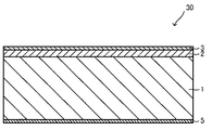
(第2の実施の形態)
図2は、第2の実施の形態による赤外光透過フィルタの一部を概略的に示す断面図である。なお、本実施形態以降、重複する説明を避けるため、第1の実施の形態と共通する点については説明を省略し、相違点を中心に説明する。
(Second Embodiment)
FIG. 2 is a cross-sectional view schematically showing a part of the infrared light transmission filter according to the second embodiment. From this embodiment onward, in order to avoid redundant description, description of points that are common to the first embodiment will be omitted, and differences will be mainly described.
図2に示すように、第2の実施の形態による赤外光透過フィルタ20においては、赤外光透過性基材1の他方の面((短)赤外光吸収膜2形成面の反対側の面)に、一方の面に誘電体多層膜からなる(長)赤外光反射膜5を形成したガラス基材4が、(長)赤外光反射膜5を外側に向けて接着剤6を介して接着されている。
As shown in FIG. 2, in the infrared
(長)赤外光反射膜5は、透過波長帯域の長波長側の光を反射して遮光する機能を有する膜、例えば、垂直に入射する光に対する反射波長帯域が860〜1100nmの膜である。この(長)赤外光反射膜5は、例えば、誘電体層Aと、誘電体層Aが有する屈折率よりも高い屈折率を有する誘電体層Bとを、スパッタリング法や真空蒸着法等により、交互に積層した誘電体多層膜から構成される。また、入射角依存性を低減するため、次のように構成してもよい。
The (long) infrared
すなわち、(長)赤外光反射膜5は、低屈折率の誘電体層Aの光学膜厚をnLdL、高屈折率の誘電体層Bの光学膜厚をnHdHとしたとき、nHdH/nLdL≧5を満足する誘電体層の層数が10以上で、かつ誘電体層の全層数が15以上である誘電体多層膜から構成してもよい。
That is, in the (long) infrared
誘電体層Aを構成する材料としては、屈折率が1.6以下、好ましくは1.2〜1.6の材料が使用される。具体的には、シリカ(SiO2)、アルミナ、フッ化ランタン、フッ化マグネシウム、六フッ化アルミニウムナトリウム等が使用される。また、誘電体層Bを構成する材料としては、屈折率が1.7以上、好ましくは1.7〜2.5の材料が使用される。具体的には、チタニア(TiO2)、ジルコニア、五酸化タンタル、五酸化ニオブ、酸化ランタン、イットリア、酸化亜鉛、硫化亜鉛等が使用される。(長)赤外光反射膜5を構成する誘電体多層膜の積層数は、通常、15〜80層、好ましくは20〜50層である。
As a material constituting the dielectric layer A, a material having a refractive index of 1.6 or less, preferably 1.2 to 1.6 is used. Specifically, silica (SiO 2 ), alumina, lanthanum fluoride, magnesium fluoride, aluminum hexafluoride sodium, or the like is used. Further, as the material constituting the dielectric layer B, a material having a refractive index of 1.7 or more, preferably 1.7 to 2.5 is used. Specifically, titania (TiO 2 ), zirconia, tantalum pentoxide, niobium pentoxide, lanthanum oxide, yttria, zinc oxide, zinc sulfide and the like are used. (Long) The number of laminated multilayer dielectric films constituting the infrared
接着剤6は、特に限定されないが、赤外光透過性基材1の特性の低下を防止し、またスループットを高める観点からは、アクリル系、エン・チオール系、エポキシ系等の光硬化型接着剤の使用が好ましく、さらに、ガラス基材4と赤外光透過性基材1との接着信頼性の観点から、光硬化型接着剤のなかでも、アクリル系、エン・チオール系が好ましい。また、その厚みも、ガラス基材4と赤外光透過性基材1との接着信頼性や、赤外光透過性基材1の歪みの発生を防止する観点から、0.1〜10μmの範囲が好ましい。
The adhesive 6 is not particularly limited, but from the viewpoint of preventing the deterioration of the characteristics of the infrared light
第2の実施の形態の赤外光透過フィルタ20においても、第1の実施の形態と同様の効果が得られる。加えて、透過波長帯域の長波長側の光を反射して遮光する(長)赤外光反射膜5を備えるので、赤外波長領域の中の特定の波長領域の光を選択的に透過させるバンドパスフィルタとして使用できる。
In the infrared
特に、垂直に入射する光に対する反射波長帯域が860〜1100nmの(長)赤外光反射膜5を設けた場合には、前述したモーションキャプチャーにさらに好適な赤外光透過特性を具備できる。
In particular, when the (long) infrared
すなわち、前述したように、上記モーションキャプチャーでは、近赤外波長領域の光が使用され、特に830〜850nmの波長帯域の光が多く使用されている。一方、誘電体多層膜の遮光特性は入射角依存性により短波長側にシフトする。したがって、このような入射角依存性を考慮して、垂直に入射する光に対する反射波長帯域が860〜1100nmの(長)赤外光反射膜5を設けることにより、830〜850nmの波長帯域の光を十分に、かつ選択的に透過でき、S/N比のさらなる向上を実現できる。
That is, as described above, in the motion capture, light in the near-infrared wavelength region is used, and in particular, light in the wavelength band of 830 to 850 nm is often used. On the other hand, the light shielding characteristics of the dielectric multilayer film shift to the short wavelength side due to the incident angle dependency. Accordingly, in consideration of such incident angle dependency, by providing the (long) infrared
なお、誘電体多層膜からなる(長)赤外光反射膜5は、図3に示す赤外光透過フィルタ30のように、接着剤6及びガラス基材4を介さず、赤外光透過性基材1の他方の面に直接設けてもよく、図2に示す赤外光透過フィルタ20と同様の効果が得られる。ただし、この場合、赤外光透過性基材1を構成する材料として、(長)赤外光反射膜5を形成する際の熱等の影響で変形したり特性が損なわれたりしないものを選択するか、あるいは、赤外光透過性基材1が変形したり特性が損なわれたりしない条件で赤外高反射膜5を形成することが好ましい。特に、赤外光透過性基材1が歪んでしまうと、それを透過してカメラに入ってくる像も歪んでしまうためジェスチャーを認識する際に誤った判定を行うおそれがある。そのため、赤外光透過性基材1に歪みが発生しない製膜方法が必要である。前記フィルタに波長830nmのレーザー光を平行光で照射した際に、レーザー光の照射中心から直径60mmの領域内に発生するニュートンリングの最大本数は8本以下が好ましい。また、具体的な製膜方法については、赤外光透過性基材1の耐熱温度以下、例えば100℃以下で、スパッタリング法、真空蒸着法、プラズマCVD法等の方法により行うことが好ましい。
Note that the (long) infrared
さらに、図示は省略したが、上記のような誘電体多層膜からなる(長)赤外光反射膜5は、(短)赤外光吸収膜2側に、すなわち、(短)赤外光吸収膜2の赤外光透過性基材1とは反対側の面に設けるようにしてもよく、図2に示す赤外光透過フィルタ20や図3に示す赤外光透過フィルタ30と同様の効果が得られる。なお、この場合も、赤外光透過性基材1を構成する材料として、(長)赤外光反射膜5を形成する際の熱等の影響で変形したり特性が損なわれたりしないものを選択するか、あるいは、赤外光透過性基材1が変形したり特性が損なわれたりしない条件で(長)赤外光反射膜5を形成することが好ましい。反射防止膜3は、赤外光透過性基材1の他方の面に形成される。
Further, although not shown, the (long) infrared
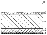
(第3の実施の形態)
図4は、第3の実施の形態による赤外光透過フィルタの一部を概略的に示す断面図である。
(Third embodiment)
FIG. 4 is a cross-sectional view schematically showing a part of the infrared light transmission filter according to the third embodiment.
図4に示すように、第3の実施の形態による赤外光透過フィルタ40においては、赤外光透過性基材1の他方の面((短)赤外光吸収膜2形成面の反対側の面)に、一方の面に誘電体多層膜からなる(短)赤外光反射膜7を形成したガラス基材4が、(短)赤外光反射膜7を外側に向けて接着剤6を介して接着されている。
As shown in FIG. 4, in the infrared
(短)赤外光反射膜7は、後述するような通常の可視光反射膜の可視光領域の光に対する遮光効果を犠牲することによって入射角依存性を低減したもので、その垂直に入射する光に対する反射波長帯域は、例えば730〜810nmである。この(短)赤外光反射膜7は、(長)赤外光反射膜5と同様、例えば、誘電体層Aと、誘電体層Aが有する屈折率よりも高い屈折率を有する誘電体層Bとを、スパッタリング法や真空蒸着法等により、交互に積層することにより形成されるが、入射角依存性を低減するため、特に次のように構成されている。
The (short) infrared
すなわち、(短)赤外光反射膜7は、低屈折率の誘電体層Aの光学膜厚をnLdL、高屈折率の誘電体層Bの光学膜厚をnHdHとしたとき、nHdH/nLdL≧5を満足する誘電体層の層数が10以上で、かつ誘電体層の全層数が15以上である誘電体多層膜から構成されている。なお、誘電体層A及び誘電体層Bを構成する材料には、(長)赤外光反射膜5を構成する誘電体多層膜の場合と同様の材料が使用される。
That is, in the (short) infrared
第3の実施の形態の赤外光透過フィルタ40においては、入射角依存性の低い(短)赤外光反射膜7を備えるので、可視光寄りの赤外光の選択透過性をより向上させることができる。
Since the infrared
なお、誘電体多層膜からなる(短)赤外光反射膜7は、図示は省略したが、接着剤6及びガラス基材4を介さず、赤外光透過性基材1の他方の面に直接設けてもよく、また、図5に示す赤外光透過フィルタ50のように、(短)赤外光吸収膜2側に、すなわち、(短)赤外光吸収膜2の赤外光透過性基材1とは反対側の面に設けるようにしてもよい(この場合、反射防止膜3は、赤外光透過性基材1の他方の面に形成される)。いずれも、図4に示す赤外光透過フィルタ40と同様の効果が得られる。ただし、これらの場合には、図3に示した赤外光透過フィルタ30等の場合と同様、赤外光透過性基材1を構成する材料として、誘電体多層膜からなる(短)赤外光反射膜7を形成する際の熱等の影響で変形したり特性が損なわれたりしないものを選択するか、あるいは、赤外光透過性基材1が変形したり特性が損なわれたりしない条件で(短)赤外光反射膜7を形成することが好ましい。具体的には、赤外光透過性基材1の耐熱温度以下、例えば100℃以下で、スパッタリング法、真空蒸着法、プラズマCVD法等の方法により行うことが好ましい。
Although the illustration of the (short) infrared
(第4の実施の形態)
図6は、第4の実施の形態による赤外光透過フィルタの一部を概略的に示す断面図である。
(Fourth embodiment)
FIG. 6 is a cross-sectional view schematically showing a part of the infrared light transmission filter according to the fourth embodiment.
図6に示すように、第4の実施の形態による赤外光透過フィルタ60においては、赤外光透過性基材1の他方の面((短)赤外光吸収膜2形成面の反対側の面)に、一方の面に誘電体多層膜からなる(短)赤外光反射膜7を形成したガラス基材4が、(短)赤外光反射膜7を外側に向けて接着剤6を介して接着される一方、(短)赤外光吸収膜2側に、すなわち、(短)赤外光吸収膜2の赤外光透過性基材1とは反対側の面に、(長)赤外光反射膜5が形成されている。
As shown in FIG. 6, in the infrared
第4の実施の形態の赤外光透過フィルタ60においては、入射角依存性の低い(短)赤外光反射膜7を備えるので、第3の実施の形態と同様、可視光寄りの赤外光の選択透過性をより向上させることができる。また、透過波長帯域の長波長側の光を反射して遮光する(長)赤外光反射膜5を備えるので、赤外波長領域の中の特定の波長領域の光を選択的に透過させるバンドパスフィルタとして使用できる。
Since the infrared
なお、本実施形態においては、図示は省略したが、誘電体多層膜からなる(短)赤外光反射膜7を、接着剤6及びガラス基材4を介さず、赤外光透過性基材1の他方の面に直接設けてもよく、また、図7に示す赤外光透過フィルタ70のように、(短)赤外光吸収膜2側に、すなわち、(短)赤外光吸収膜2の赤外光透過性基材1とは反対側の面に設けるようにしてもよい(この場合、赤外光透過性基材1の他方の面に(長)赤外光反射膜5が形成される)。いずれも、図6に示す赤外光透過フィルタ60と同様の効果が得られる。これらの場合にも、図3に示した赤外光透過フィルタ30等の場合と同様、赤外光透過性基材1を構成する材料として、誘電体多層膜からなる(短)赤外光反射膜7を形成する際の熱等の影響で変形したり特性が損なわれたりしないものを選択するか、あるいは、赤外光透過性基材1が変形したり特性が損なわれたりしない条件で(短)赤外光反射膜7を形成することが好ましい。具体的には、赤外光透過性基材1の耐熱温度以下、例えば100℃以下で、スパッタリング法、真空蒸着法、プラズマCVD法等の方法により行うことが好ましい。
In the present embodiment, although not shown, the (short) infrared
(第5の実施の形態)
図8は、第5の実施の形態による赤外光透過フィルタの一部を概略的に示す断面図である。
(Fifth embodiment)
FIG. 8 is a cross-sectional view schematically showing a part of the infrared light transmission filter according to the fifth embodiment.
図8に示すように、第5の実施の形態による赤外光透過フィルタ80においては、第2の実施形態と同様のガラス基材4の一方の面に、可視波長領域、例えば400〜700nmの波長領域の光を反射する誘電体多層膜からなる可視光反射膜8を設け、他方の面に第1の実施の形態の赤外光透過フィルタ10と同様の(短)赤外光吸収膜2を形成した構造を有する。(短)赤外光吸収膜2上には、さらに、反射防止膜3を設けている。この実施形態においては、ガラス基材4及び可視光反射膜8が、第1の実施の形態における赤外光透過性基材1としての機能を有している。
As shown in FIG. 8, in the infrared
第5の実施の形態の赤外光透過フィルタ80においては、第1の実施の形態と同様の効果が得られる上に、ガラス基材4及び可視光反射膜8を赤外光透過性基材1として機能させているので、第1〜第4の実施の形態に比べて、全体の厚みをより薄肉にできる利点を有する。さらに、(短)赤外光吸収膜2によって、誘電体多層膜からなる可視光反射膜8の分光特性の入射角依存性が実質的に低減される。
In the infrared
(第6の実施の形態)
図9は、第6の実施の形態による赤外光透過フィルタの一部を概略的に示す断面図である。
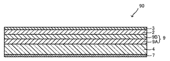
(Sixth embodiment)
FIG. 9 is a cross-sectional view schematically showing a part of the infrared light transmission filter according to the sixth embodiment.
図9に示すように、本実施形態による赤外光透過フィルタ90は、第5の実施の形態による赤外光透過フィルタ80において、ガラス基材4と(短)赤外光吸収膜2の間に、可視光乃至近赤外線吸収剤を含む1層乃至複数層からなる光吸収膜9を介在させるとともに、可視光反射膜8に代えて、入射角依存性の低い誘電体多層膜からなる(短)赤外光反射膜7を備えた構造を有する。図9の例では、光吸収膜9は、ガラス基材4側の可視光吸収剤を含む可視光吸収膜9Aと、(短)赤外光吸収膜2側の、(短)赤外光吸収膜2に含まれるものと異なる近赤外線吸収剤を含む(短)赤外光吸収膜9Bから構成されている(以下、本実施形態の説明において、理解を容易にするため、(短)赤外光吸収膜2を第1の(短)赤外光吸収膜、(短)赤外光吸収膜9Bを第2の(短)赤外光吸収膜、第1の(短)赤外光吸収膜2に含まれる近赤外線吸収剤を第1の近赤外線吸収剤、第2の(短)赤外光吸収膜9Bに含まれる近赤外線吸収剤を第2の近赤外線吸収剤と称する。)。この実施形態においては、ガラス基材4及び光吸収膜9が、第1の実施の形態における赤外光透過性基材1としての機能を有している。
As shown in FIG. 9, the infrared
可視光吸収膜9Aは、可視光吸収剤を含む透明樹脂から構成される。また、第2の(短)赤外光吸収膜9Bは、第2の近赤外線吸収剤を含む透明樹脂から構成される。透明樹脂及び可視光吸収剤としては、赤外光透過性基材1で用いたものと同様のものを使用できる。また、第2の近赤外線吸収剤としては、近赤外領域の光を吸収するものであれば特に制限なく使用されるが、可視光吸収剤と第1の近赤外線吸収剤を光吸収特性を補完して、赤外光透過フィルタ70に良好な赤外選択透過性を付与し得るものが好ましい。
The visible light absorbing film 9A is made of a transparent resin containing a visible light absorber. The second (short) infrared
可視光吸収膜9Aにおける可視光吸収剤の含有量は10〜60質量%が好ましく、20〜50質量%がより好ましい。可視光吸収剤の含有量が10質量%未満では可視光吸収能が十分得られないおそれがあり、60質量%を超えると可視光吸収剤の透明樹脂への溶解性や樹脂の膜質が低下するおそれがある。また、第2の(短)赤外光吸収膜9Bにおける第2の近赤外線吸収剤の含有量は、0.1〜10質量%が好ましく、0.5〜5質量%がより好ましい。近赤外線吸収剤の含有量が0.1質量%未満では使用による効果が十分に得られないおそれがあり、10質量%を超えると赤外波長領域の光の透過性が低下するおそれがある。
The visible light absorber content in the visible light absorbing film 9A is preferably 10 to 60% by mass, and more preferably 20 to 50% by mass. If the content of the visible light absorber is less than 10% by mass, sufficient visible light absorption ability may not be obtained. If the content exceeds 60% by mass, the solubility of the visible light absorber in the transparent resin and the resin film quality are deteriorated. There is a fear. Moreover, 0.1-10 mass% is preferable and, as for content of the 2nd near-infrared absorber in the 2nd (short) infrared
可視光吸収膜9A及び第2の(短)赤外光吸収膜9Bには、それぞれ可視光吸収剤及び第2の近赤外線吸収剤の他に、本発明の効果を阻害しない範囲で、赤外光透過性基材1で用いたものと同様の添加剤、例えば、紫外線吸収剤、酸化防止剤、レベリング剤、消泡剤、帯電防止剤、熱安定剤、分散剤、難燃剤、滑剤、可塑剤等が含有されていてもよい。
The visible light absorbing film 9A and the second (short) infrared
可視光吸収膜9A及び第2の(短)赤外光吸収膜9Bは、第1の(短)赤外光吸収膜2の場合と同様の方法で形成できる。また、それらの各厚みは、いずれも0.01〜500μmの範囲が好ましく、0.05〜50μmの範囲がより好ましい。0.01μm未満では、所定の吸収能が得られないおそれがあり、また、500μmを超えると、乾燥時に乾燥ムラが生じるおそれがある。
The visible
第6の実施の形態の赤外光透過フィルタ90においては、第1の実施の形態と同様の効果が得られる上に、ガラス基材4及び光吸収膜9を赤外光透過性基材1として機能させているので、第1〜第4の実施の形態に比べて、全体の厚みをより薄肉にできる利点を有する。さらに、本実施形態では、可視光吸収膜9A及び第2の(短)赤外光吸収膜9B、さらに入射角依存性の低い(短)赤外光反射膜7を備えるので、第5の実施の形態に比べて、より良好な赤外光選択透過性を具備できる。
In the infrared
なお、本実施形態においては、図10に示す赤外光透過フィルタ100のように、(短)赤外光吸収膜2上に、反射防止膜3に代えて透過波長帯域の長波長側の光を反射して遮光する(長)赤外光反射膜5を設けるようにしてもよい。このような赤外光透過フィルタ100においては、第2及び第4の実施の形態の赤外光透過フィルタと同様、赤外波長領域の中の特定の波長領域の光を選択的に透過させるバンドパスフィルタとして使用できる。
In the present embodiment, as in the infrared
また、図示を省略したが、場合により、第1の(短)赤外光吸収膜2、可視光吸収膜9A及び第2の(短)赤外光吸収膜9Bを、単層構造としたり、あるいは第1の(短)赤外光吸収膜2と第2の(短)赤外光吸収膜9Bを単層とし、これに可視光吸収膜9Aを積層するようにしてもよい。さらに、各吸収膜の積層順等も特に限定されるものではない。
Although not shown, the first (short) infrared
以上、本発明のいくつかの実施形態を説明したが、本発明は、以上説明した実施の形態の記載内容に限定されるものではなく、本発明の要旨を逸脱しない範囲で適宜変更可能であることはいうまでもない。 As mentioned above, although several embodiment of this invention was described, this invention is not limited to the content of description of embodiment described above, In the range which does not deviate from the summary of this invention, it can change suitably. Needless to say.
次に、本発明を実施例によりさらに詳細に説明するが、本発明はこれらの実施例に何ら限定されない。なお、実施例及び比較例における赤外光透過フィルタや赤外光透過性基材等の分光透過率曲線は、分光光度計(大塚電子(株)MCPD−3000)を用いて測定した。 EXAMPLES Next, although an Example demonstrates this invention still in detail, this invention is not limited to these Examples at all. In addition, the spectral transmittance curves, such as an infrared-light transmissive filter in an Example and a comparative example, and an infrared-light transmissive base material, were measured using the spectrophotometer (Otsuka Electronics Co., Ltd. MCPD-3000).
(実施例1)
約760nmに光吸収端を有する近赤外線吸収剤(山田化学工業(株)製 商品名「NIR−43V」)とポリエステル樹脂(東洋紡績(株)製、商品名「バイロン103」;屈折率1.60〜1.61)とをシクロヘキサノンに溶解し、近赤外線吸収剤1質量%及びポリエステル樹脂99質量%を含有する溶液を調製した。この溶液を、厚さ1mmの赤外光透過性基材(三菱レイヨン(株)製 商品名「アクリフィルターIR75」)の一方の面にスピンコータ(ミカサ(株)製 スピンコータMS−A200)を用いて塗布し、100℃で1分間加熱乾燥させて、厚さ15μmの(短)赤外光吸収膜を形成した。
Example 1
A near-infrared absorber having a light absorption edge at about 760 nm (trade name “NIR-43V” manufactured by Yamada Chemical Co., Ltd.) and a polyester resin (trade name “Byron 103” manufactured by Toyobo Co., Ltd.); 60 to 1.61) were dissolved in cyclohexanone to prepare a solution containing 1% by mass of a near infrared absorber and 99% by mass of a polyester resin. Using this solution, a spin coater (Spin Coater MS-A200 manufactured by Mikasa Co., Ltd.) was applied to one surface of a 1 mm thick infrared light transmissive substrate (trade name “Acryfilter IR75” manufactured by Mitsubishi Rayon Co., Ltd.). It was applied and dried by heating at 100 ° C. for 1 minute to form a (short) infrared light absorbing film having a thickness of 15 μm.
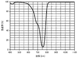
次いで、この(短)赤外光吸収膜を形成した赤外光透過性基材の両面に、シリカ、チタニアからなる厚さ約580nmの5層反射防止膜を形成し、赤外光透過フィルタを得た。 Next, a five-layer antireflection film made of silica and titania and having a thickness of about 580 nm is formed on both sides of the infrared light transmitting base material on which the (short) infrared light absorbing film is formed. Obtained.
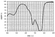
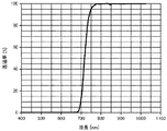
得られた赤外光透過フィルタの分光透過率曲線を測定した。結果を図11に示す。また、上記赤外光透過性基材について測定した分光透過率曲線を図12に、(短)赤外光吸収膜について測定した内部透過率曲線を図13に示す。 The spectral transmittance curve of the obtained infrared light transmission filter was measured. The results are shown in FIG. Further, FIG. 12 shows a spectral transmittance curve measured for the infrared light transmissive substrate, and FIG. 13 shows an internal transmittance curve measured for the (short) infrared light absorbing film.
これらの図から明らかなように、(短)赤外光吸収膜が形成される前の赤外光透過性基材では、約720nmまでの波長領域における透過率は約0%、約820nm以上の波長領域における透過率は90%以上で、これらの領域間(約720〜約820nm)で透過率が緩やかに変化していたのに対し、実施例1で得られた赤外光透過フィルタでは、400〜770nmの波長領域における透過率が約0%、830〜900nmの波長領域における透過率は95%以上で、透過率はこれらの領域間(約770〜約830nm)で十分に急峻に変化しており、約760nmに光吸収端を有する近赤外線吸収剤を含む(短)赤外光吸収膜を形成したことにより、赤外光透過性基材の短波長側の光に対する遮光特性の向上が確認された。 As is clear from these figures, in the infrared light transmitting base material before the (short) infrared light absorbing film is formed, the transmittance in the wavelength region up to about 720 nm is about 0%, about 820 nm or more. The transmittance in the wavelength region is 90% or more, and the transmittance gradually changed between these regions (about 720 to about 820 nm), whereas in the infrared light transmission filter obtained in Example 1, The transmittance in the wavelength region of 400 to 770 nm is about 0%, the transmittance in the wavelength region of 830 to 900 nm is 95% or more, and the transmittance changes sufficiently sharply between these regions (about 770 to about 830 nm). In addition, by forming a (short) infrared light absorption film containing a near infrared absorber having a light absorption edge at about 760 nm, an improvement in the light shielding property against light on the short wavelength side of the infrared light transmissive substrate is achieved. confirmed.
(比較例)
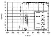
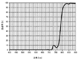
厚さ0.3mmのガラス基板(B270(ショット製))の一方の面に、真空蒸着法により、シリカ(SiO2;屈折率1.45(波長830nm))層とチタニア(TiO2;屈折率2.25(波長830nm))層とを交互に積層して、表1に示すような構成からなる誘電体多層膜(31層)を形成し、赤外光透過フィルタを得た。
(Comparative example)
A silica (SiO 2 ; refractive index 1.45 (wavelength 830 nm)) layer and titania (TiO 2 ; refractive index) were formed on one surface of a 0.3 mm thick glass substrate (B270 (manufactured by Shot)) by vacuum deposition. 2.25 (wavelength: 830 nm)) layers were alternately laminated to form a dielectric multilayer film (31 layers) having a configuration as shown in Table 1 to obtain an infrared light transmission filter.

得られた赤外光透過フィルタの分光透過率曲線(入射角度0度、入射角度20度及び40度のP偏光及びS偏光)を測定した。結果を図14に示す。 Spectral transmittance curves (P-polarized light and S-polarized light having an incident angle of 0 degree, an incident angle of 20 degrees, and 40 degrees) of the obtained infrared light transmission filter were measured. The results are shown in FIG.
図14から明らかなように、比較例で得られた赤外光透過フィルタは、入射角度0度の入射光に対しては、実施例1と同等の遮光特性を示すが、入射角度が変わると透過率曲線も変動しており、入射角度±40度の範囲では、実施例1で用いた赤外光透過性基材(「アクリフィルターIR75」)と同等の遮光特性を示した。 As is clear from FIG. 14, the infrared light transmission filter obtained in the comparative example shows the same light shielding characteristic as that of Example 1 with respect to incident light with an incident angle of 0 degrees, but the incident angle changes. The transmittance curve also fluctuated, and in the range of the incident angle ± 40 degrees, the light shielding characteristics equivalent to those of the infrared light transmissive substrate (“Acryfilter IR75”) used in Example 1 were exhibited.
この図から明らかなように、誘電多層膜での遮光フィルタの課題である入射角度0度と±40度では遮光波長が70nm以上も可視光側に移動しており、十分に可視光の遮光をしているとは言い難い。 As is clear from this figure, at the incident angles of 0 ° and ± 40 °, which is a problem of the light shielding filter in the dielectric multilayer film, the light shielding wavelength is moved to the visible light side by 70 nm or more, and the visible light is sufficiently shielded. It ’s hard to say.
(実施例2)
約760nmに光吸収端を有する近赤外線吸収剤(山田化学工業(株)製 商品名「NIR−43V」)と、ポリエステル樹脂(東洋紡績(株)製、商品名 バイロン103;屈折率1.60〜1.61)とをシクロヘキサノンに溶解し、近赤外線吸収剤1質量%及びポリエステル樹脂99質量%を含有する溶液を調製した。この溶液を、厚さ1mmの赤外光透過性基材(三菱レイヨン(株)製 商品名「アクリフィルターIR75」)の一方の面にスピンコータ(ミカサ(株)製 スピンコータMS−A200)を用いて塗布し、100℃で1分間加熱乾燥させて、厚さ15μmの(短)赤外光吸収膜を形成した。
(Example 2)
Near-infrared absorber having a light absorption edge at about 760 nm (trade name “NIR-43V” manufactured by Yamada Chemical Co., Ltd.) and polyester resin (trade name Byron 103 manufactured by Toyobo Co., Ltd .; refractive index 1.60) -1.61) were dissolved in cyclohexanone to prepare a solution containing 1% by mass of a near infrared absorber and 99% by mass of a polyester resin. Using this solution, a spin coater (Spin Coater MS-A200 manufactured by Mikasa Co., Ltd.) was applied to one surface of a 1 mm thick infrared light transmissive substrate (trade name “Acryfilter IR75” manufactured by Mitsubishi Rayon Co., Ltd.). It was applied and dried by heating at 100 ° C. for 1 minute to form a (short) infrared light absorbing film having a thickness of 15 μm.
また、厚さ0.3mmのガラス基板(B270(ショット製))の一方の面に、真空蒸着法により、シリカ(SiO2;屈折率1.45)層とチタニア(TiO2;屈折率2.25)層とを交互に積層して、表2に示すような構成からなる誘電体多層膜(23層)を形成した。 Further, a silica (SiO 2 ; refractive index 1.45) layer and titania (TiO 2 ; refractive index 2) are formed on one surface of a glass substrate (B270 (manufactured by Shot)) having a thickness of 0.3 mm by vacuum deposition. 25) Layers were alternately laminated to form a dielectric multilayer film (23 layers) having the structure shown in Table 2.
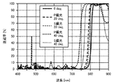
この誘電体多層膜を形成したガラス基板の他方の面(誘電体多層膜非形成面)に、紫外線硬化型接着剤を約10μmの厚さに塗布し、その上に上記の(短)赤外光吸収膜を形成した赤外光透過性基材を、(短)赤外光吸収膜非形成面側をガラス基板に向けて積層し、ガラス基板側から紫外線を照射して紫外線硬化型接着剤を硬化させ、一体に接着した。その後、(短)赤外光吸収膜の表面にシリカ、チタニアからなる厚さ約580nmの5層反射防止膜を形成し、赤外光透過フィルタを得た。 An ultraviolet curable adhesive is applied to the other surface of the glass substrate on which the dielectric multilayer film is formed (the surface on which the dielectric multilayer film is not formed) to a thickness of about 10 μm, and the above (short) infrared is applied thereon. An ultraviolet light curable adhesive is formed by laminating an infrared light transmissive base material on which a light absorption film is formed with the (short) infrared light absorption film non-forming surface side facing the glass substrate and irradiating ultraviolet light from the glass substrate side. Was cured and bonded together. Thereafter, a five-layer antireflection film made of silica and titania having a thickness of about 580 nm was formed on the surface of the (short) infrared light absorption film to obtain an infrared light transmission filter.
得られた赤外光透過フィルタの分光透過率曲線を測定した。結果を図15に示す。また、誘電体多層膜を形成したガラス基板について測定した分光透過率曲線(入射角度0度、入射角度20度及び40度のP偏光及びS偏光)を図16に示す。 The spectral transmittance curve of the obtained infrared light transmission filter was measured. The results are shown in FIG. In addition, FIG. 16 shows spectral transmittance curves (P-polarized light and S-polarized light having an incident angle of 0 degree, an incident angle of 20 degrees, and 40 degrees) measured for the glass substrate on which the dielectric multilayer film is formed.
図15から明らかなように、実施例2で得られた赤外光透過フィルタは、400〜770nm及び970〜1100nmの両波長領域における透過率が約0%、810〜920nmの波長領域における透過率が87%以上で、約770〜約810nm及び約920〜約970nmの非常に狭い波長領域で透過率が変化しており、(短)赤外光吸収膜と、図16に示すような分光特性を有する誘電体多層膜形成ガラス基板を設けたことにより、810〜920nmの波長領域における光を選択的に透過させるバンドパスフィルタとして高い特性を有することが確認された。この赤外光透過フィルタは、半導体レーザ(LD)等から830〜850nmの波長の光を被写体に当て、その反射光を赤外線カメラで撮像し、演算処理することにより、被写体のジェスチャーを認識するモーションキャプチャー等の用途に非常に有用である。 As is clear from FIG. 15, the infrared light transmission filter obtained in Example 2 has a transmittance of about 0% in both wavelength regions of 400 to 770 nm and 970 to 1100 nm, and a transmittance in the wavelength region of 810 to 920 nm. Is 87% or more, and the transmittance changes in a very narrow wavelength region of about 770 to about 810 nm and about 920 to about 970 nm. The (short) infrared light absorption film and the spectral characteristics as shown in FIG. By providing the dielectric multilayer film-formed glass substrate having the above, it was confirmed that the film has high characteristics as a band-pass filter that selectively transmits light in the wavelength region of 810 to 920 nm. This infrared light transmission filter applies light with a wavelength of 830 to 850 nm to a subject from a semiconductor laser (LD) or the like, captures the reflected light with an infrared camera, and performs arithmetic processing to recognize a gesture of the subject. It is very useful for applications such as capture.
また、この例では長波長側で入射角度依存性がみられるが、撮像素子の感度の弱い波長領域であるため可視光側と比べ入射角度依存性による遮光波長の変化は赤外線カメラのS/N比に大きくは影響しない。 In this example, the incident angle dependence is observed on the long wavelength side. However, since it is a wavelength region where the sensitivity of the image pickup device is weak, the change in the light shielding wavelength due to the incident angle dependence compared to the visible light side is the S / N of the infrared camera. The ratio is not greatly affected.
(実施例3)
厚さ0.3mmのガラス基板(B270(ショット製))の一方の面に、スパッタリング法により、シリカ(SiO2;屈折率1.45)層とチタニア(TiO2;屈折率2.25)層とを交互に積層して、表3に示すような構成からなる誘電体多層膜(39層)を形成した。
Example 3
A silica (SiO 2 ; refractive index 1.45) layer and titania (TiO 2 ; refractive index 2.25) layer are formed on one surface of a glass substrate (B270 (made by Shot)) having a thickness of 0.3 mm by sputtering. Were alternately laminated to form a dielectric multilayer film (39 layers) having the structure shown in Table 3.
この誘電体多層膜を形成したガラス基板の他方の面(誘電体多層膜非形成面)に、実施例1と同様に調製した、約760nmに光吸収端を有する近赤外線吸収剤(「NIR−43V」)1質量%、及びポリエステル樹脂(「バイロン103」)99質量%を含有する溶液を、スピンコータ(「スピンコータMS−A200」)を用いて塗布し、100℃で1分間加熱乾燥させて、厚さ15μmの(短)赤外光吸収膜を形成した。その後、(短)赤外光吸収膜の表面にシリカ、チタニアからなる厚さ約580nmの反射防止膜を形成し、赤外光透過フィルタを得た。 A near-infrared absorber having a light absorption edge at about 760 nm (“NIR−”) was prepared in the same manner as in Example 1 on the other surface (the surface where the dielectric multilayer film was not formed) of the glass substrate on which the dielectric multilayer film was formed. 43V ") 1% by mass and a solution containing 99% by mass of a polyester resin (" Byron 103 ") were applied using a spin coater (" Spin Coater MS-A200 ") and dried by heating at 100 ° C for 1 minute. A (short) infrared light absorbing film having a thickness of 15 μm was formed. Thereafter, an antireflection film made of silica and titania and having a thickness of about 580 nm was formed on the surface of the (short) infrared light absorption film to obtain an infrared light transmission filter.
得られた赤外光透過フィルタの分光透過率曲線(入射角度0度、入射角度20度及び40度のP偏光及びS偏光)を測定した。結果を図17に示す。また、誘電体多層膜を形成したガラス基板について測定した分光透過率曲線(入射角度0度、入射角度20度及び40度のP偏光及びS偏光)を図18に示す。 Spectral transmittance curves (P-polarized light and S-polarized light having an incident angle of 0 degree, an incident angle of 20 degrees, and 40 degrees) of the obtained infrared light transmission filter were measured. The results are shown in FIG. Further, FIG. 18 shows spectral transmittance curves (P-polarized light and S-polarized light having an incident angle of 0 degree, an incident angle of 20 degrees, and 40 degrees) measured on the glass substrate on which the dielectric multilayer film is formed.
図17から明らかなように、実施例3で得られた赤外光透過フィルタは、約760〜約810nmの非常に狭い波長領域で透過率が変化しており、しかも、入射角依存性も低減されている。 As is clear from FIG. 17, the infrared light transmission filter obtained in Example 3 has a change in transmittance in a very narrow wavelength region of about 760 to about 810 nm, and the dependency on the incident angle is also reduced. Has been.
(実施例4)
厚さ0.3mmのガラス基板(B270(ショット製))の一方の面に、スパッタリング法により、シリカ(SiO2;屈折率1.46)層と酸化タンタル(Ta2O5;屈折率2.14)層とを交互に積層して、表4に示すような構成からなる誘電体多層膜(38層)を形成した。
Example 4
A silica (SiO 2 ; refractive index 1.46) layer and tantalum oxide (Ta 2 O 5 ; refractive index 2) are formed on one surface of a 0.3 mm thick glass substrate (B270 (made by Schott)) by sputtering. 14) Layers were alternately laminated to form a dielectric multilayer film (38 layers) having the structure shown in Table 4.
また、可視光吸収剤(稲畑産業(株)製 商品名「AI7100」)とポリエステル樹脂(東洋紡績(株)製、商品名「バイロン103」;屈折率1.60〜1.61)とをシクロヘキサノンに溶解し、可視光吸収剤40質量%及びポリエステル樹脂60質量%を含有する溶液(I)を調製した。同様にして、約720nmに光吸収端を有する近赤外線吸収剤1質量%及びポリエステル樹脂99質量%を含有する溶液(II)、及び、約760nmに光吸収端を有する近赤外線吸収剤(QCR Solutions Corp製 商品名「NIR757A」)1質量%及びポリエステル樹脂99質量%を含有する溶液(III)を調製した。 Further, a visible light absorber (trade name “AI7100” manufactured by Inabata Sangyo Co., Ltd.) and a polyester resin (trade name “Byron 103” manufactured by Toyobo Co., Ltd .; refractive index 1.60 to 1.61) are combined with cyclohexanone. And a solution (I) containing 40% by mass of a visible light absorber and 60% by mass of a polyester resin was prepared. Similarly, a solution (II) containing 1% by weight of a near-infrared absorber having a light absorption edge at about 720 nm and 99% by weight of a polyester resin, and a near-infrared absorber having a light absorption edge at about 760 nm (QCR Solutions) A solution (III) containing 1% by mass of a trade name “NIR757A” manufactured by Corp and 99% by mass of a polyester resin was prepared.
次いで、これらの溶液(I)〜(III)を、溶液(I)、溶液(II)、溶液(III)の順に、上記の誘電体多層膜を形成したガラス基板の他方の面(誘電体多層膜非形成面)にスピンコータ(ミカサ(株)製 スピンコータMS−A200)を用いて塗布し、それぞれ100℃で1分間加熱乾燥させて、厚さ300μmの光吸収膜(I)、厚さ50μmの光吸収膜(II)、及び厚さ25μmの光吸収膜(III)を形成した。 Subsequently, these solutions (I) to (III) are applied in the order of solution (I), solution (II), and solution (III) to the other surface (dielectric multilayer) of the glass substrate on which the dielectric multilayer film is formed. The film is formed on a non-film-forming surface using a spin coater (Spin Coater MS-A200 manufactured by Mikasa Co., Ltd.) and heated and dried at 100 ° C. for 1 minute, respectively, to form a light absorbing film (I) having a thickness of 300 μm, A light absorbing film (II) and a light absorbing film (III) having a thickness of 25 μm were formed.
その後、上記光吸収膜(III)の表面に、シリカ、チタニアからなる厚さ約580nmの5層反射防止膜を形成し、赤外光透過フィルタを得た。 Thereafter, a 5-layer antireflection film made of silica and titania and having a thickness of about 580 nm was formed on the surface of the light absorption film (III) to obtain an infrared light transmission filter.
得られた赤外光透過フィルタの分光透過率曲線(入射角度0度、入射角度20度、30度及び40度のP偏光及びS偏光)を測定した。結果を図19に示す。また、誘電体多層膜を形成したガラス基板について測定した分光透過率曲線(入射角度0度、入射角度10度、20度、30度及び40度のP偏光、S偏光及び平均(Ave))を図20に示す。さらに、光吸収膜(I)の内部透過率曲線を図21に、光吸収膜(II)の内部透過率曲線を図22に、光吸収膜(III)の内部透過率曲線を図23に、光吸収膜(I)〜(III)全体の内部透過率曲線を図24に示す。
Spectral transmittance curves (P-polarized light and S-polarized light having an incident angle of 0 degree, incident angles of 20 degrees, 30 degrees, and 40 degrees) of the obtained infrared light transmission filter were measured. The results are shown in FIG. Further, spectral transmittance curves (P-polarized light, S-polarized light and average (Ave) of
図19から明らかなように、実施例4で得られた赤外光透過フィルタは、約760〜約810nmの非常に狭い波長領域で透過率が変化しており、かつ入射角依存性は実施例3に比べ、より低減されている。 As is clear from FIG. 19, the infrared light transmission filter obtained in Example 4 has a transmittance changing in a very narrow wavelength region of about 760 to about 810 nm, and the incident angle dependency is in the example. Compared to 3, it is further reduced.
本発明の赤外光透過フィルタは、製造コストが安く、十分な小型化、薄型化を図ることができ、また、従来の反射型フィルタのような入射角依存性等の問題がなく、さらに、赤外光透過特性にも十分に優れることから、赤外線リモコン、赤外線通信、赤外線カメラ、赤外線カメラを内蔵した光学システム等の赤外光透過フィルタとして好適に利用できる。 The infrared light transmission filter of the present invention is low in manufacturing cost, can be sufficiently downsized and thinned, and has no problems such as incident angle dependency as in the conventional reflection type filter. Since it is sufficiently excellent in infrared light transmission characteristics, it can be suitably used as an infrared light transmission filter for an infrared remote control, infrared communication, an infrared camera, an optical system incorporating an infrared camera, or the like.
1…赤外光透過性基材、2…(第1の)(短)赤外光吸収膜、3…反射防止膜、4…ガラス基板、5…(長)赤外光反射膜、6…接着剤、7…(短)赤外光反射膜、8…可視光反射膜、9A…可視光吸収膜、9B…(第2の)(短)赤外光吸収膜、10,20,30,40,50,60,70,80,90,100…赤外光透過フィルタ。
DESCRIPTION OF
Claims (11)
D’(%/nm)=[T810(%)−T760(%)]/[810(nm)−760(nm)]
(式中、T810は、分光透過率曲線における波長810nmの透過率であり、T760は、分光透過率曲線における波長760nmの透過率である) The infrared light transmission filter according to any one of claims 1 to 9, wherein a transmittance change amount D 'represented by the following formula is 1% / nm or more.
D ′ (% / nm) = [T 810 (%) − T 760 (%)] / [810 (nm) −760 (nm)]
(Where T 810 is the transmittance at a wavelength of 810 nm in the spectral transmittance curve, and T 760 is the transmittance at a wavelength of 760 nm in the spectral transmittance curve)
Priority Applications (2)
| Application Number | Priority Date | Filing Date | Title |
|---|---|---|---|
| JP2011163519A JP5741283B2 (en) | 2010-12-10 | 2011-07-26 | Infrared light transmission filter and imaging apparatus using the same |
| US13/302,475 US9570490B2 (en) | 2010-12-10 | 2011-11-22 | Infrared transmission filter and imaging device |
Applications Claiming Priority (3)
| Application Number | Priority Date | Filing Date | Title |
|---|---|---|---|
| JP2010276082 | 2010-12-10 | ||
| JP2010276082 | 2010-12-10 | ||
| JP2011163519A JP5741283B2 (en) | 2010-12-10 | 2011-07-26 | Infrared light transmission filter and imaging apparatus using the same |
Publications (2)
| Publication Number | Publication Date |
|---|---|
| JP2012137728A true JP2012137728A (en) | 2012-07-19 |
| JP5741283B2 JP5741283B2 (en) | 2015-07-01 |
Family
ID=46198375
Family Applications (1)
| Application Number | Title | Priority Date | Filing Date |
|---|---|---|---|
| JP2011163519A Active JP5741283B2 (en) | 2010-12-10 | 2011-07-26 | Infrared light transmission filter and imaging apparatus using the same |
Country Status (2)
| Country | Link |
|---|---|
| US (1) | US9570490B2 (en) |
| JP (1) | JP5741283B2 (en) |
Cited By (28)
| Publication number | Priority date | Publication date | Assignee | Title |
|---|---|---|---|---|
| WO2014034386A1 (en) * | 2012-08-29 | 2014-03-06 | 旭硝子株式会社 | Near-infrared cutoff filter |
| JP2014052604A (en) * | 2012-09-10 | 2014-03-20 | Nippon Shokubai Co Ltd | Light selective transmission filter, base material therefor, and application thereof |
| WO2014168189A1 (en) * | 2013-04-10 | 2014-10-16 | 旭硝子株式会社 | Infrared-blocking filter |
| WO2015005447A1 (en) * | 2013-07-12 | 2015-01-15 | 富士フイルム株式会社 | Near infrared absorption composition, near infrared-cut filter and manufacturing method therefor, and solid state image pickup element |
| WO2015166873A1 (en) * | 2014-05-01 | 2015-11-05 | 富士フイルム株式会社 | Infrared sensor, near-infrared absorbent composition, photosensitive resin composition, compound, near-infrared absorbent filter, and imaging device |
| JP2016075886A (en) * | 2014-10-06 | 2016-05-12 | 采▲ぎょく▼科技股▲ふん▼有限公司VisEra Technologies Company Limited | Stack filter and image sensor including the same |
| KR20160094299A (en) * | 2015-01-30 | 2016-08-09 | 제이에스알 가부시끼가이샤 | Solid state imaging device and optical filter |
| WO2016143824A1 (en) * | 2015-03-10 | 2016-09-15 | 富士フイルム株式会社 | Composition kit, layered body and method for manufacturing same, and bandpass filter |
| JP2016200771A (en) * | 2015-04-14 | 2016-12-01 | Jsr株式会社 | Optical filter and device using optical filter |
| JP2017096998A (en) * | 2015-11-18 | 2017-06-01 | 株式会社ジャパンディスプレイ | Display device |
| US9679933B2 (en) | 2014-10-06 | 2017-06-13 | Visera Technologies Company Limited | Image sensors and methods of forming the same |
| JPWO2016098810A1 (en) * | 2014-12-19 | 2017-09-28 | 旭硝子株式会社 | Optical filter and apparatus using the same |
| WO2017213047A1 (en) * | 2016-06-08 | 2017-12-14 | Jsr株式会社 | Optical filter and optical sensor device |
| JPWO2016178346A1 (en) * | 2015-05-01 | 2018-03-29 | 富士フイルム株式会社 | Film, film manufacturing method, solid-state imaging device, and infrared sensor |
| JP2018120192A (en) * | 2017-01-27 | 2018-08-02 | 京セラ株式会社 | Infrared band-pass filter and optical semiconductor device |
| JP2018170801A (en) * | 2017-02-21 | 2018-11-01 | 株式会社ナノルクス | Solid state imaging device and imaging apparatus |
| JP2019032503A (en) * | 2017-08-07 | 2019-02-28 | 杭州美迪凱光電科技有限公司 | Coating type narrow-band filter having absorbent material |
| WO2019039386A1 (en) * | 2017-08-25 | 2019-02-28 | 富士フイルム株式会社 | Optical filter and optical sensor |
| JP2019039957A (en) * | 2017-08-22 | 2019-03-14 | 株式会社トプコン | Optical filter and calibration method for measuring device using the same |
| JP2019514233A (en) * | 2016-01-25 | 2019-05-30 | ショット グラス テクノロジーズ (スゾウ) カンパニー リミテッドSchott Glass Technologies (Suzhou) Co., Ltd. | Optical parameter detection system |
| JP2019124946A (en) * | 2019-02-18 | 2019-07-25 | Jsr株式会社 | Optical filter and device using optical filter |
| WO2020017495A1 (en) * | 2018-07-17 | 2020-01-23 | Agc株式会社 | Optical member |
| KR20200037219A (en) | 2017-07-31 | 2020-04-08 | 제이에스알 가부시끼가이샤 | Photoelectric conversion device |
| JP2020056873A (en) * | 2018-10-01 | 2020-04-09 | キヤノン電子株式会社 | Optical filter and imaging apparatus |
| JP2020056875A (en) * | 2018-10-01 | 2020-04-09 | キヤノン電子株式会社 | Optical filter, imaging apparatus, and optical sensor |
| JPWO2019116843A1 (en) * | 2017-12-12 | 2020-12-17 | Jsr株式会社 | Cover member and electronic device with authentication function |
| WO2022230917A1 (en) * | 2021-04-30 | 2022-11-03 | 豊田合成株式会社 | Infrared light–transmitting product |
| JP7331635B2 (en) | 2018-11-06 | 2023-08-23 | Jsr株式会社 | Optical filter and its use |
Families Citing this family (29)
| Publication number | Priority date | Publication date | Assignee | Title |
|---|---|---|---|---|
| CN202177716U (en) * | 2011-07-22 | 2012-03-28 | 浙江水晶光电科技股份有限公司 | Optical filter used for high pixel image system |
| TW202300961A (en) | 2012-07-16 | 2023-01-01 | 美商唯亞威方案公司 | Optical filter and sensor system |
| KR102056613B1 (en) * | 2012-08-23 | 2019-12-17 | 에이지씨 가부시키가이샤 | Near-infrared cut filter and solid-state imaging device |
| CN105102560A (en) * | 2012-12-28 | 2015-11-25 | 富士胶片株式会社 | Curable resin composition for forming infrared-reflecting film, infrared-reflecting film and manufacturing method therefor, infrared cut-off filter, and solid-state imaging element using same |
| KR101527822B1 (en) * | 2013-09-06 | 2015-06-10 | 주식회사 엘엠에스 | Optical filter and image pickup device comprising the same |
| US20150116576A1 (en) * | 2013-10-30 | 2015-04-30 | Blackberry Limited | Image capture assembly, digital camera and a mobile device having an improved construction |
| US9349770B2 (en) * | 2014-02-11 | 2016-05-24 | Semiconductor Components Industries, Llc | Imaging systems with infrared pixels having increased quantum efficiency |
| TW201600574A (en) * | 2014-06-30 | 2016-01-01 | Fujifilm Corp | Near infrared ray absorptive composition, near infrared ray cut filter and manufacturing method thereof, solid image pickup element and camera module |
| KR102305998B1 (en) * | 2014-12-08 | 2021-09-28 | 엘지이노텍 주식회사 | Image processing apparatus |
| WO2016114362A1 (en) * | 2015-01-14 | 2016-07-21 | 旭硝子株式会社 | Near-infrared cut filter and solid-state imaging device |
| WO2016114363A1 (en) * | 2015-01-14 | 2016-07-21 | 旭硝子株式会社 | Near-infrared cut filter and imaging device |
| US10466395B1 (en) * | 2016-09-21 | 2019-11-05 | Apple Inc. | Systems with matte infrared-transparent layers |
| CN206339678U (en) * | 2016-12-26 | 2017-07-18 | 信阳舜宇光学有限公司 | Cutoff filter |
| CN107065053B (en) * | 2017-05-24 | 2019-10-15 | 信阳舜宇光学有限公司 | The method for preparing optical filter |
| DE102017113535A1 (en) | 2017-06-20 | 2018-12-20 | Osram Opto Semiconductors Gmbh | Semiconductor sensor |
| CN107172338B (en) * | 2017-06-30 | 2021-01-15 | 联想(北京)有限公司 | Camera and electronic equipment |
| US10247865B2 (en) | 2017-07-24 | 2019-04-02 | Viavi Solutions Inc. | Optical filter |
| CN107479190B (en) * | 2017-08-15 | 2019-08-16 | 天津津航技术物理研究所 | A kind of visible light and LONG WAVE INFRARED all dielectric film recombination dichroic elements and design method |
| CN107515438B (en) * | 2017-09-06 | 2020-09-08 | 天津津航技术物理研究所 | Infrared wide-spectrum cut-off narrow-band laser light splitting element |
| JP6259155B1 (en) * | 2017-10-03 | 2018-01-10 | 日本板硝子株式会社 | Optical filter and imaging device |
| US11314005B2 (en) * | 2018-05-17 | 2022-04-26 | Apple Inc. | Electronic device with infrared transparent one-way mirror |
| US10845508B2 (en) * | 2018-05-31 | 2020-11-24 | Microsoft Technology Licensing, Llc | Optical stack including embedded diffuse surface |
| CN110824599B (en) | 2018-08-14 | 2021-09-03 | 白金科技股份有限公司 | Infrared band-pass filter |
| CN112543881B (en) * | 2018-09-03 | 2022-12-27 | Jsr株式会社 | Optical filter |
| CN110989183B (en) * | 2019-12-30 | 2021-08-03 | 长春理工大学 | Spectroscope for marine multi-dimensional imaging system, preparation method and design method thereof |
| US11086170B1 (en) * | 2020-05-20 | 2021-08-10 | Himax Display, Inc. | Display device |
| TWI752677B (en) | 2020-11-12 | 2022-01-11 | 晶瑞光電股份有限公司 | IR Cut Filter Structure |
| CN112596140B (en) * | 2020-11-26 | 2022-11-01 | 中国航空工业集团公司洛阳电光设备研究所 | Infrared long-wave cut-off filter and preparation method thereof |
| CN113050212A (en) * | 2021-01-12 | 2021-06-29 | 苏州群烨新材料科技有限公司 | Infrared band-pass filter, preparation method thereof and imaging device with infrared band-pass filter |
Citations (11)
| Publication number | Priority date | Publication date | Assignee | Title |
|---|---|---|---|---|
| JPS60139757A (en) * | 1983-12-28 | 1985-07-24 | Mitsubishi Rayon Co Ltd | Resin composition for filter transmitting near-infrared rays |
| JPS63270765A (en) * | 1986-12-26 | 1988-11-08 | Mitsui Toatsu Chem Inc | Phthalocyanine compound and resin composition containing same |
| JP2000314807A (en) * | 1999-04-30 | 2000-11-14 | Nippon Shinku Kogaku Kk | Visible light shielding and infrared ray transmitting filter |
| JP2001183523A (en) * | 1999-12-27 | 2001-07-06 | Toyobo Co Ltd | Near infrared ray absorbing filter |
| JP2005338395A (en) * | 2004-05-26 | 2005-12-08 | Jsr Corp | Near ir ray cut-off filter and its manufacturing method |
| JP2006165493A (en) * | 2004-11-12 | 2006-06-22 | Tokai Kogaku Kk | Infrared beam receiving and emitting unit, manufacturing method thereof and electronic apparatus provided therewith |
| JP2006343631A (en) * | 2005-06-10 | 2006-12-21 | Toyo Ink Mfg Co Ltd | Near infrared absorbing composition for solid state imaging device and solid state imaging device using the same |
| JP2007079349A (en) * | 2005-09-16 | 2007-03-29 | Toray Ind Inc | Optical filter |
| JP2007264116A (en) * | 2006-03-27 | 2007-10-11 | Mitsumi Electric Co Ltd | Camera module for infrared sensor |
| JP2008224926A (en) * | 2007-03-12 | 2008-09-25 | Nippon Shokubai Co Ltd | Near-infrared ray absorption coating agent |
| JP2008230969A (en) * | 2007-03-16 | 2008-10-02 | Nippon Shokubai Co Ltd | Borate and visible light-absorbing material, luminous material |
Family Cites Families (19)
| Publication number | Priority date | Publication date | Assignee | Title |
|---|---|---|---|---|
| US3579130A (en) * | 1969-07-18 | 1971-05-18 | Vern N Smiley | Thin film active interference filter |
| US3926835A (en) * | 1971-03-02 | 1975-12-16 | American Cyanamid Co | Infrared transmitting filter containing 1,4,5,8-tetracyclohexylaminoanthraquinone |
| JPS597043A (en) * | 1982-07-06 | 1984-01-14 | 株式会社豊田中央研究所 | Heat-wave shielding laminate |
| JPS62903A (en) * | 1985-06-05 | 1987-01-06 | Sumitomo Chem Co Ltd | Near infrared ray absorbing filter |
| US4778731A (en) * | 1987-02-13 | 1988-10-18 | Northrop Corporation | Optically transparent electrically conductive semiconductor windows and methods of manufacture |
| US5233464A (en) * | 1991-03-20 | 1993-08-03 | Costich Verne R | Multilayer infrared filter |
| FR2810118B1 (en) * | 2000-06-07 | 2005-01-21 | Saint Gobain Vitrage | TRANSPARENT SUBSTRATE HAVING ANTIREFLECTION COATING |
| JP2002175020A (en) * | 2000-09-29 | 2002-06-21 | Fuji Photo Film Co Ltd | Optical filter and image display device |
| DE50207927D1 (en) * | 2001-01-26 | 2006-10-05 | Zeiss Carl Smt Ag | NARROW-BAND SPECTRAL FILTER AND ITS USE |
| DE10141102A1 (en) * | 2001-08-22 | 2003-04-03 | Schott Glas | Cadmium-free optical steep edge filters |
| GB2396436B (en) * | 2002-12-19 | 2006-06-28 | Thales Plc | An optical filter |
| US7081991B2 (en) * | 2003-03-14 | 2006-07-25 | Rockwell Collins, Inc. | Dye-based filter |
| JP2006153976A (en) | 2004-11-25 | 2006-06-15 | Nippon Shinku Kogaku Kk | Infra-red light transmission filter |
| WO2007049478A1 (en) * | 2005-10-26 | 2007-05-03 | Central Glass Company, Limited | Near infrared ray reflective substrate and near infrared ray reflective laminated glass employing that substrate, near infrared ray reflective double layer glass |
| KR101047946B1 (en) * | 2006-10-25 | 2011-07-12 | 주식회사 엘지화학 | Electromagnetic shielding film having a transparent function and a near infrared ray absorption function, an optical filter comprising the same, and a plasma display panel comprising the same |
| KR100953556B1 (en) * | 2007-02-08 | 2010-04-21 | 주식회사 엘지화학 | Pdp filter for absorbing near infrared ray |
| WO2009025297A1 (en) * | 2007-08-22 | 2009-02-26 | Mitsubishi Chemical Corporation | Resin black matrix, light blocking photosensitive resin composition, tft element substrate and liquid crystal display device |
| TWI418839B (en) * | 2009-09-24 | 2013-12-11 | Largan Precision Co Ltd | Near infra-red imaging lens assembly |
| JP6076261B2 (en) * | 2011-01-28 | 2017-02-08 | メルク パテント ゲゼルシャフト ミット ベシュレンクテル ハフツングMerck Patent Gesellschaft mit beschraenkter Haftung | Layer arrangement to control light transmission |
-
2011
- 2011-07-26 JP JP2011163519A patent/JP5741283B2/en active Active
- 2011-11-22 US US13/302,475 patent/US9570490B2/en active Active
Patent Citations (11)
| Publication number | Priority date | Publication date | Assignee | Title |
|---|---|---|---|---|
| JPS60139757A (en) * | 1983-12-28 | 1985-07-24 | Mitsubishi Rayon Co Ltd | Resin composition for filter transmitting near-infrared rays |
| JPS63270765A (en) * | 1986-12-26 | 1988-11-08 | Mitsui Toatsu Chem Inc | Phthalocyanine compound and resin composition containing same |
| JP2000314807A (en) * | 1999-04-30 | 2000-11-14 | Nippon Shinku Kogaku Kk | Visible light shielding and infrared ray transmitting filter |
| JP2001183523A (en) * | 1999-12-27 | 2001-07-06 | Toyobo Co Ltd | Near infrared ray absorbing filter |
| JP2005338395A (en) * | 2004-05-26 | 2005-12-08 | Jsr Corp | Near ir ray cut-off filter and its manufacturing method |
| JP2006165493A (en) * | 2004-11-12 | 2006-06-22 | Tokai Kogaku Kk | Infrared beam receiving and emitting unit, manufacturing method thereof and electronic apparatus provided therewith |
| JP2006343631A (en) * | 2005-06-10 | 2006-12-21 | Toyo Ink Mfg Co Ltd | Near infrared absorbing composition for solid state imaging device and solid state imaging device using the same |
| JP2007079349A (en) * | 2005-09-16 | 2007-03-29 | Toray Ind Inc | Optical filter |
| JP2007264116A (en) * | 2006-03-27 | 2007-10-11 | Mitsumi Electric Co Ltd | Camera module for infrared sensor |
| JP2008224926A (en) * | 2007-03-12 | 2008-09-25 | Nippon Shokubai Co Ltd | Near-infrared ray absorption coating agent |
| JP2008230969A (en) * | 2007-03-16 | 2008-10-02 | Nippon Shokubai Co Ltd | Borate and visible light-absorbing material, luminous material |
Cited By (51)
| Publication number | Priority date | Publication date | Assignee | Title |
|---|---|---|---|---|
| JPWO2014034386A1 (en) * | 2012-08-29 | 2016-08-08 | 旭硝子株式会社 | Near-infrared cut filter |
| CN104583820A (en) * | 2012-08-29 | 2015-04-29 | 旭硝子株式会社 | Near-infrared cutoff filter |
| WO2014034386A1 (en) * | 2012-08-29 | 2014-03-06 | 旭硝子株式会社 | Near-infrared cutoff filter |
| US10073202B2 (en) | 2012-08-29 | 2018-09-11 | Asahi Glass Company, Limited | Near-infrared cut filter |
| JP2014052604A (en) * | 2012-09-10 | 2014-03-20 | Nippon Shokubai Co Ltd | Light selective transmission filter, base material therefor, and application thereof |
| WO2014168189A1 (en) * | 2013-04-10 | 2014-10-16 | 旭硝子株式会社 | Infrared-blocking filter |
| JPWO2014168189A1 (en) * | 2013-04-10 | 2017-02-16 | 旭硝子株式会社 | Infrared shielding filter |
| WO2015005447A1 (en) * | 2013-07-12 | 2015-01-15 | 富士フイルム株式会社 | Near infrared absorption composition, near infrared-cut filter and manufacturing method therefor, and solid state image pickup element |
| JP2016014845A (en) * | 2013-07-12 | 2016-01-28 | 富士フイルム株式会社 | Near infrared absorbing composition, near infrared cut filter, method for manufacturing the same, and solid-state image sensing device |
| WO2015166873A1 (en) * | 2014-05-01 | 2015-11-05 | 富士フイルム株式会社 | Infrared sensor, near-infrared absorbent composition, photosensitive resin composition, compound, near-infrared absorbent filter, and imaging device |
| JPWO2015166873A1 (en) * | 2014-05-01 | 2017-04-20 | 富士フイルム株式会社 | Infrared sensor, near infrared absorbing composition, photosensitive resin composition, compound, near infrared absorbing filter, and imaging device |
| JP2016075886A (en) * | 2014-10-06 | 2016-05-12 | 采▲ぎょく▼科技股▲ふん▼有限公司VisEra Technologies Company Limited | Stack filter and image sensor including the same |
| US9679933B2 (en) | 2014-10-06 | 2017-06-13 | Visera Technologies Company Limited | Image sensors and methods of forming the same |
| US9666620B2 (en) | 2014-10-06 | 2017-05-30 | Visera Technologies Company Limited | Stacked filter and image sensor containing the same |
| JPWO2016098810A1 (en) * | 2014-12-19 | 2017-09-28 | 旭硝子株式会社 | Optical filter and apparatus using the same |
| JP2016146619A (en) * | 2015-01-30 | 2016-08-12 | Jsr株式会社 | Solid-state image pickup device and optical filter |
| KR102464660B1 (en) * | 2015-01-30 | 2022-11-08 | 제이에스알 가부시끼가이샤 | Solid state imaging device and optical filter |
| KR20160094299A (en) * | 2015-01-30 | 2016-08-09 | 제이에스알 가부시끼가이샤 | Solid state imaging device and optical filter |
| WO2016143824A1 (en) * | 2015-03-10 | 2016-09-15 | 富士フイルム株式会社 | Composition kit, layered body and method for manufacturing same, and bandpass filter |
| JPWO2016143824A1 (en) * | 2015-03-10 | 2017-12-28 | 富士フイルム株式会社 | COMPOSITION KIT, LAMINATE, MANUFACTURING METHOD THEREOF, BANDPASS FILTER |
| TWI697545B (en) * | 2015-03-10 | 2020-07-01 | 日商富士軟片股份有限公司 | Composition kit, laminate and method for producing the same, band-pass filter |
| JP2016200771A (en) * | 2015-04-14 | 2016-12-01 | Jsr株式会社 | Optical filter and device using optical filter |
| JPWO2016178346A1 (en) * | 2015-05-01 | 2018-03-29 | 富士フイルム株式会社 | Film, film manufacturing method, solid-state imaging device, and infrared sensor |
| JP2017096998A (en) * | 2015-11-18 | 2017-06-01 | 株式会社ジャパンディスプレイ | Display device |
| JP2019514233A (en) * | 2016-01-25 | 2019-05-30 | ショット グラス テクノロジーズ (スゾウ) カンパニー リミテッドSchott Glass Technologies (Suzhou) Co., Ltd. | Optical parameter detection system |
| KR20190015282A (en) * | 2016-06-08 | 2019-02-13 | 제이에스알 가부시끼가이샤 | Optical filters and optical sensor devices |
| TWI792256B (en) * | 2016-06-08 | 2023-02-11 | 日商Jsr股份有限公司 | Optical filter and optical sensing device |
| US11163098B2 (en) | 2016-06-08 | 2021-11-02 | Jsr Corporation | Optical filter and optical sensor device |
| WO2017213047A1 (en) * | 2016-06-08 | 2017-12-14 | Jsr株式会社 | Optical filter and optical sensor device |
| JPWO2017213047A1 (en) * | 2016-06-08 | 2019-04-04 | Jsr株式会社 | Optical filter and optical sensor device |
| KR102425315B1 (en) * | 2016-06-08 | 2022-07-27 | 제이에스알 가부시끼가이샤 | Optical Filters and Optical Sensor Devices |
| JP2020177253A (en) * | 2016-06-08 | 2020-10-29 | Jsr株式会社 | Optical filter and optical sensor device |
| JP2018120192A (en) * | 2017-01-27 | 2018-08-02 | 京セラ株式会社 | Infrared band-pass filter and optical semiconductor device |
| JP2018170801A (en) * | 2017-02-21 | 2018-11-01 | 株式会社ナノルクス | Solid state imaging device and imaging apparatus |
| US10819922B2 (en) | 2017-02-21 | 2020-10-27 | Nanolux Co. Ltd. | Solid-state imaging element and imaging device |
| KR20200037219A (en) | 2017-07-31 | 2020-04-08 | 제이에스알 가부시끼가이샤 | Photoelectric conversion device |
| JP2019032503A (en) * | 2017-08-07 | 2019-02-28 | 杭州美迪凱光電科技有限公司 | Coating type narrow-band filter having absorbent material |
| JP2019039957A (en) * | 2017-08-22 | 2019-03-14 | 株式会社トプコン | Optical filter and calibration method for measuring device using the same |
| US11543569B2 (en) | 2017-08-25 | 2023-01-03 | Fujifilm Corporation | Optical filter and optical sensor |
| JPWO2019039386A1 (en) * | 2017-08-25 | 2020-10-01 | 富士フイルム株式会社 | Optical filter and optical sensor |
| TWI796355B (en) * | 2017-08-25 | 2023-03-21 | 日商富士軟片股份有限公司 | Optical Filters and Light Sensors |
| WO2019039386A1 (en) * | 2017-08-25 | 2019-02-28 | 富士フイルム株式会社 | Optical filter and optical sensor |
| JPWO2019116843A1 (en) * | 2017-12-12 | 2020-12-17 | Jsr株式会社 | Cover member and electronic device with authentication function |
| WO2020017495A1 (en) * | 2018-07-17 | 2020-01-23 | Agc株式会社 | Optical member |
| JPWO2020017495A1 (en) * | 2018-07-17 | 2021-08-19 | Agc株式会社 | Optical member |
| JP7298073B2 (en) | 2018-07-17 | 2023-06-27 | Agc株式会社 | Optical member |
| JP2020056875A (en) * | 2018-10-01 | 2020-04-09 | キヤノン電子株式会社 | Optical filter, imaging apparatus, and optical sensor |
| JP2020056873A (en) * | 2018-10-01 | 2020-04-09 | キヤノン電子株式会社 | Optical filter and imaging apparatus |
| JP7331635B2 (en) | 2018-11-06 | 2023-08-23 | Jsr株式会社 | Optical filter and its use |
| JP2019124946A (en) * | 2019-02-18 | 2019-07-25 | Jsr株式会社 | Optical filter and device using optical filter |
| WO2022230917A1 (en) * | 2021-04-30 | 2022-11-03 | 豊田合成株式会社 | Infrared light–transmitting product |
Also Published As
| Publication number | Publication date |
|---|---|
| US20120145901A1 (en) | 2012-06-14 |
| JP5741283B2 (en) | 2015-07-01 |
| US9570490B2 (en) | 2017-02-14 |
Similar Documents
| Publication | Publication Date | Title |
|---|---|---|
| JP5741283B2 (en) | Infrared light transmission filter and imaging apparatus using the same | |
| US10495796B2 (en) | Near-infrared cut filter | |
| JP6332403B2 (en) | Optical filter and solid-state imaging device | |
| JP5013022B2 (en) | Infrared cut filter | |
| JP5741347B2 (en) | Optical filter and imaging apparatus using the same | |
| JP6589061B2 (en) | Camera structure, imaging device | |
| JP5849719B2 (en) | Light absorber and imaging device using the same | |
| WO2016171219A1 (en) | Optical filter and imaging device | |
| WO2014103921A1 (en) | Ir cut filter and image capture device including same | |
| CN105074513A (en) | Near-infrared cut filter and solid-state image pickup device including same | |
| CN110095831A (en) | Cutoff filter and photographic device | |
| CN108700688B (en) | Laminated structure of glass cover plate, camera structure and imaging device | |
| CN104871047A (en) | Near-infrared cut-off filter | |
| WO2014061188A1 (en) | Image-capturing element and image-capturing device | |
| WO2019189039A1 (en) | Optical filter | |
| WO2020004641A1 (en) | Optical filter and information acquisition device | |
| US20220291423A1 (en) | Optical device having optical and mechanical properties | |
| CN112444898B (en) | Optical filter for wide-angle application | |
| JP2006106570A (en) | Light absorbing filter | |
| CN109416420A (en) | Optical goods and its optical filter | |
| JP6136661B2 (en) | Near-infrared cut filter | |
| JP6156468B2 (en) | Light absorber and imaging device using the same | |
| WO2023157403A1 (en) | Optical filter and imaging device | |
| JP2017227774A (en) | Optical filter and light-amount adjustment device, as well as optical device |
Legal Events
| Date | Code | Title | Description |
|---|---|---|---|
| A621 | Written request for application examination |
Free format text: JAPANESE INTERMEDIATE CODE: A621 Effective date: 20140305 |
|
| A977 | Report on retrieval |
Free format text: JAPANESE INTERMEDIATE CODE: A971007 Effective date: 20141121 |
|
| A131 | Notification of reasons for refusal |
Free format text: JAPANESE INTERMEDIATE CODE: A131 Effective date: 20141202 |
|
| A521 | Request for written amendment filed |
Free format text: JAPANESE INTERMEDIATE CODE: A523 Effective date: 20150128 |
|
| TRDD | Decision of grant or rejection written | ||
| A01 | Written decision to grant a patent or to grant a registration (utility model) |
Free format text: JAPANESE INTERMEDIATE CODE: A01 Effective date: 20150331 |
|
| A61 | First payment of annual fees (during grant procedure) |
Free format text: JAPANESE INTERMEDIATE CODE: A61 Effective date: 20150413 |
|
| R150 | Certificate of patent or registration of utility model |
Ref document number: 5741283 Country of ref document: JP Free format text: JAPANESE INTERMEDIATE CODE: R150 |
|
| S533 | Written request for registration of change of name |
Free format text: JAPANESE INTERMEDIATE CODE: R313533 |
|
| R350 | Written notification of registration of transfer |
Free format text: JAPANESE INTERMEDIATE CODE: R350 |
|
| R250 | Receipt of annual fees |
Free format text: JAPANESE INTERMEDIATE CODE: R250 |
|
| R250 | Receipt of annual fees |
Free format text: JAPANESE INTERMEDIATE CODE: R250 |
|
| R250 | Receipt of annual fees |
Free format text: JAPANESE INTERMEDIATE CODE: R250 |
|
| R250 | Receipt of annual fees |
Free format text: JAPANESE INTERMEDIATE CODE: R250 |
|
| R250 | Receipt of annual fees |
Free format text: JAPANESE INTERMEDIATE CODE: R250 |