JP2012134498A - Circuit board mount structure and method for multilayer ceramic capacitor, land pattern of circuit board, and package and alignment method for multilayer ceramic capacitor - Google Patents
Circuit board mount structure and method for multilayer ceramic capacitor, land pattern of circuit board, and package and alignment method for multilayer ceramic capacitor Download PDFInfo
- Publication number
- JP2012134498A JP2012134498A JP2011276870A JP2011276870A JP2012134498A JP 2012134498 A JP2012134498 A JP 2012134498A JP 2011276870 A JP2011276870 A JP 2011276870A JP 2011276870 A JP2011276870 A JP 2011276870A JP 2012134498 A JP2012134498 A JP 2012134498A
- Authority
- JP
- Japan
- Prior art keywords
- multilayer ceramic
- ceramic capacitor
- mlcc
- land
- circuit board
- Prior art date
- Legal status (The legal status is an assumption and is not a legal conclusion. Google has not performed a legal analysis and makes no representation as to the accuracy of the status listed.)
- Pending
Links
- 239000003985 ceramic capacitor Substances 0.000 title claims abstract description 257
- 238000000034 method Methods 0.000 title claims abstract description 60
- 239000004020 conductor Substances 0.000 claims abstract description 49
- 239000000758 substrate Substances 0.000 claims abstract description 22
- 238000004806 packaging method and process Methods 0.000 claims description 17
- 238000012546 transfer Methods 0.000 claims description 15
- 238000005476 soldering Methods 0.000 claims description 8
- 230000007423 decrease Effects 0.000 claims description 7
- 230000008569 process Effects 0.000 claims description 6
- 229920006280 packaging film Polymers 0.000 claims description 3
- 239000012785 packaging film Substances 0.000 claims description 3
- 238000010276 construction Methods 0.000 claims 1
- 229910000679 solder Inorganic materials 0.000 description 12
- 238000010586 diagram Methods 0.000 description 9
- 230000000694 effects Effects 0.000 description 8
- 239000000463 material Substances 0.000 description 7
- 238000012360 testing method Methods 0.000 description 7
- 230000009467 reduction Effects 0.000 description 6
- 230000009471 action Effects 0.000 description 4
- 230000005540 biological transmission Effects 0.000 description 4
- 239000000919 ceramic Substances 0.000 description 4
- 230000008859 change Effects 0.000 description 4
- 229910002113 barium titanate Inorganic materials 0.000 description 3
- JRPBQTZRNDNNOP-UHFFFAOYSA-N barium titanate Chemical compound [Ba+2].[Ba+2].[O-][Ti]([O-])([O-])[O-] JRPBQTZRNDNNOP-UHFFFAOYSA-N 0.000 description 3
- 238000010030 laminating Methods 0.000 description 3
- 230000005389 magnetism Effects 0.000 description 3
- 229910052751 metal Inorganic materials 0.000 description 3
- 239000002184 metal Substances 0.000 description 3
- 230000003247 decreasing effect Effects 0.000 description 2
- 230000005684 electric field Effects 0.000 description 2
- 230000005611 electricity Effects 0.000 description 2
- 238000011156 evaluation Methods 0.000 description 2
- 239000007769 metal material Substances 0.000 description 2
- 229910052759 nickel Inorganic materials 0.000 description 2
- 229910052763 palladium Inorganic materials 0.000 description 2
- 239000003990 capacitor Substances 0.000 description 1
- 229910010293 ceramic material Inorganic materials 0.000 description 1
- 239000011248 coating agent Substances 0.000 description 1
- 238000000576 coating method Methods 0.000 description 1
- 229910052802 copper Inorganic materials 0.000 description 1
- 230000002596 correlated effect Effects 0.000 description 1
- 230000000875 corresponding effect Effects 0.000 description 1
- 238000006073 displacement reaction Methods 0.000 description 1
- 230000005489 elastic deformation Effects 0.000 description 1
- 238000005516 engineering process Methods 0.000 description 1
- 238000003475 lamination Methods 0.000 description 1
- 238000005259 measurement Methods 0.000 description 1
- 238000010295 mobile communication Methods 0.000 description 1
- 238000012986 modification Methods 0.000 description 1
- 230000004048 modification Effects 0.000 description 1
- 238000007747 plating Methods 0.000 description 1
- 230000003405 preventing effect Effects 0.000 description 1
- 238000012545 processing Methods 0.000 description 1
- 230000005855 radiation Effects 0.000 description 1
- 238000005245 sintering Methods 0.000 description 1
- 239000010409 thin film Substances 0.000 description 1
- 238000004804 winding Methods 0.000 description 1
Images


Classifications
-
- H—ELECTRICITY
- H01—ELECTRIC ELEMENTS
- H01G—CAPACITORS; CAPACITORS, RECTIFIERS, DETECTORS, SWITCHING DEVICES, LIGHT-SENSITIVE OR TEMPERATURE-SENSITIVE DEVICES OF THE ELECTROLYTIC TYPE
- H01G2/00—Details of capacitors not covered by a single one of groups H01G4/00-H01G11/00
- H01G2/02—Mountings
- H01G2/06—Mountings specially adapted for mounting on a printed-circuit support
- H01G2/065—Mountings specially adapted for mounting on a printed-circuit support for surface mounting, e.g. chip capacitors
-
- H—ELECTRICITY
- H01—ELECTRIC ELEMENTS
- H01G—CAPACITORS; CAPACITORS, RECTIFIERS, DETECTORS, SWITCHING DEVICES, LIGHT-SENSITIVE OR TEMPERATURE-SENSITIVE DEVICES OF THE ELECTROLYTIC TYPE
- H01G4/00—Fixed capacitors; Processes of their manufacture
- H01G4/002—Details
- H01G4/228—Terminals
- H01G4/232—Terminals electrically connecting two or more layers of a stacked or rolled capacitor
-
- H—ELECTRICITY
- H01—ELECTRIC ELEMENTS
- H01G—CAPACITORS; CAPACITORS, RECTIFIERS, DETECTORS, SWITCHING DEVICES, LIGHT-SENSITIVE OR TEMPERATURE-SENSITIVE DEVICES OF THE ELECTROLYTIC TYPE
- H01G4/00—Fixed capacitors; Processes of their manufacture
- H01G4/30—Stacked capacitors
-
- H—ELECTRICITY
- H05—ELECTRIC TECHNIQUES NOT OTHERWISE PROVIDED FOR
- H05K—PRINTED CIRCUITS; CASINGS OR CONSTRUCTIONAL DETAILS OF ELECTRIC APPARATUS; MANUFACTURE OF ASSEMBLAGES OF ELECTRICAL COMPONENTS
- H05K13/00—Apparatus or processes specially adapted for manufacturing or adjusting assemblages of electric components
- H05K13/02—Feeding of components
- H05K13/022—Feeding of components with orientation of the elements
-
- H—ELECTRICITY
- H05—ELECTRIC TECHNIQUES NOT OTHERWISE PROVIDED FOR
- H05K—PRINTED CIRCUITS; CASINGS OR CONSTRUCTIONAL DETAILS OF ELECTRIC APPARATUS; MANUFACTURE OF ASSEMBLAGES OF ELECTRICAL COMPONENTS
- H05K3/00—Apparatus or processes for manufacturing printed circuits
- H05K3/30—Assembling printed circuits with electric components, e.g. with resistor
- H05K3/32—Assembling printed circuits with electric components, e.g. with resistor electrically connecting electric components or wires to printed circuits
- H05K3/34—Assembling printed circuits with electric components, e.g. with resistor electrically connecting electric components or wires to printed circuits by soldering
- H05K3/341—Surface mounted components
- H05K3/3431—Leadless components
- H05K3/3442—Leadless components having edge contacts, e.g. leadless chip capacitors, chip carriers
-
- H—ELECTRICITY
- H05—ELECTRIC TECHNIQUES NOT OTHERWISE PROVIDED FOR
- H05K—PRINTED CIRCUITS; CASINGS OR CONSTRUCTIONAL DETAILS OF ELECTRIC APPARATUS; MANUFACTURE OF ASSEMBLAGES OF ELECTRICAL COMPONENTS
- H05K2201/00—Indexing scheme relating to printed circuits covered by H05K1/00
- H05K2201/10—Details of components or other objects attached to or integrated in a printed circuit board
- H05K2201/10007—Types of components
- H05K2201/10015—Non-printed capacitor
-
- H—ELECTRICITY
- H05—ELECTRIC TECHNIQUES NOT OTHERWISE PROVIDED FOR
- H05K—PRINTED CIRCUITS; CASINGS OR CONSTRUCTIONAL DETAILS OF ELECTRIC APPARATUS; MANUFACTURE OF ASSEMBLAGES OF ELECTRICAL COMPONENTS
- H05K2203/00—Indexing scheme relating to apparatus or processes for manufacturing printed circuits covered by H05K3/00
- H05K2203/16—Inspection; Monitoring; Aligning
- H05K2203/166—Alignment or registration; Control of registration
-
- Y—GENERAL TAGGING OF NEW TECHNOLOGICAL DEVELOPMENTS; GENERAL TAGGING OF CROSS-SECTIONAL TECHNOLOGIES SPANNING OVER SEVERAL SECTIONS OF THE IPC; TECHNICAL SUBJECTS COVERED BY FORMER USPC CROSS-REFERENCE ART COLLECTIONS [XRACs] AND DIGESTS
- Y02—TECHNOLOGIES OR APPLICATIONS FOR MITIGATION OR ADAPTATION AGAINST CLIMATE CHANGE
- Y02P—CLIMATE CHANGE MITIGATION TECHNOLOGIES IN THE PRODUCTION OR PROCESSING OF GOODS
- Y02P70/00—Climate change mitigation technologies in the production process for final industrial or consumer products
- Y02P70/50—Manufacturing or production processes characterised by the final manufactured product
-
- Y—GENERAL TAGGING OF NEW TECHNOLOGICAL DEVELOPMENTS; GENERAL TAGGING OF CROSS-SECTIONAL TECHNOLOGIES SPANNING OVER SEVERAL SECTIONS OF THE IPC; TECHNICAL SUBJECTS COVERED BY FORMER USPC CROSS-REFERENCE ART COLLECTIONS [XRACs] AND DIGESTS
- Y10—TECHNICAL SUBJECTS COVERED BY FORMER USPC
- Y10T—TECHNICAL SUBJECTS COVERED BY FORMER US CLASSIFICATION
- Y10T29/00—Metal working
- Y10T29/49—Method of mechanical manufacture
- Y10T29/49002—Electrical device making
- Y10T29/49117—Conductor or circuit manufacturing
- Y10T29/49124—On flat or curved insulated base, e.g., printed circuit, etc.
Landscapes
- Engineering & Computer Science (AREA)
- Power Engineering (AREA)
- Microelectronics & Electronic Packaging (AREA)
- Manufacturing & Machinery (AREA)
- Fixed Capacitors And Capacitor Manufacturing Machines (AREA)
- Ceramic Capacitors (AREA)
- Supply And Installment Of Electrical Components (AREA)
- Electric Connection Of Electric Components To Printed Circuits (AREA)
- Structures For Mounting Electric Components On Printed Circuit Boards (AREA)
Abstract
Description
本発明は、積層セラミックキャパシタの回路基板実装構造、実装方法及びこのため回路基板のランドパターン、水平方向にテーピングした積層セラミックキャパシタの包装体並びに水平方向整列方法に関する。特に、内部電極が設けられた誘電体シートが積層され、該内部電極と並列接続する外部端子電極が両端部に設けられた積層セラミックキャパシタの回路基板への実装方法であって、該回路基板の表面に積層セラミックキャパシタが実装されるランドを設け、積層セラミックキャパシタの内部電極層と回路基板が水平方向になるように配置して、外部端子電極とランドとを導電接続し、外部端子電極とランドとを導電接続する導電材の高さ(Ts)は、積層セラミックキャパシタの厚さ(TMLCC)の1/3未満にすることによって、振動騒音を大きく減少させることができる積層セラミックキャパシタの回路基板実装構造、実装方法及びこのため回路基板のランドパターン、水平方向にテーピングした積層セラミックキャパシタの包装体並びに水平方向整列方法に関する。 The present invention relates to a circuit board mounting structure of a multilayer ceramic capacitor, a mounting method thereof, a land pattern of the circuit board, a packaging body of the multilayer ceramic capacitor taped in the horizontal direction, and a horizontal alignment method. In particular, a method for mounting a multilayer ceramic capacitor on a circuit board in which dielectric sheets provided with internal electrodes are laminated and external terminal electrodes connected in parallel with the internal electrodes are provided at both ends, A land on which the multilayer ceramic capacitor is mounted is provided on the surface, the internal electrode layer of the multilayer ceramic capacitor and the circuit board are arranged in a horizontal direction, and the external terminal electrode and the land are conductively connected. The height (T s ) of the conductive material for conductively connecting the two is less than 1/3 of the thickness (T MLCC ) of the multilayer ceramic capacitor, so that the vibration noise can be greatly reduced. Circuit board mounting structure, mounting method, and circuit board land pattern, packaged multilayer ceramic capacitor taped horizontally And a horizontal alignment method.
一般に、積層型セラミックキャパシタ(MuLti−Layered Ceramic Capacitor:MLCC)は、移動通信端末、ノート型パソコン、パソコン、携帯端末(PDA)など多くの電子製品の印刷回路基板に取り付けられ、電気を充電または放電させる重要な役目をするチップ形態のコンデンサーであって、その使用用途及び容量によって多様な大きさ及び積層形態を取っている。 In general, a multilayer ceramic capacitor (MLC) is attached to a printed circuit board of many electronic products such as mobile communication terminals, notebook computers, personal computers, and portable terminals (PDAs) to charge or discharge electricity. It is a chip-type capacitor that plays an important role, and has various sizes and laminated forms depending on the intended use and capacity.
一般に、積層型セラミックキャパシタは、複数の誘電体層間に異なる極性の内部電極が交互に積層された構造を有する。 In general, a multilayer ceramic capacitor has a structure in which internal electrodes having different polarities are alternately stacked between a plurality of dielectric layers.
このような積層型セラミックキャパシタは、小型化が可能で、且つ高容量が保障され、実装が容易という長所があるので、多様な電子装置の部品として広く使われている。 Such a multilayer ceramic capacitor is widely used as a component of various electronic devices because it can be reduced in size, has a high capacity, and is easy to mount.
積層型セラミックキャパシタの積層体を設けるセラミック材料として、誘電率の比較的高いチタン酸バリウムなどの強誘電体材料が一般的に利用されている。このような強誘電体材料は、圧電性及び電歪性を有するため、強誘電体材料に電界が加えられると、応力及び機械的変形が振動として現われ、積層セラミックキャパシタの端子電極から基板側へと該振動が伝達されることになる。 A ferroelectric material such as barium titanate having a relatively high dielectric constant is generally used as a ceramic material for providing a multilayer ceramic capacitor laminate. Since such a ferroelectric material has piezoelectricity and electrostriction, when an electric field is applied to the ferroelectric material, stress and mechanical deformation appear as vibration, and the terminal electrode of the multilayer ceramic capacitor is moved to the substrate side. And the vibration is transmitted.
すなわち、積層セラミックキャパシタに交流電圧が加えられた場合には、該積層セラミックキャパシタの素子本体にX、Y、Zの各方向に沿って応力(Fx、Ft、Fz)が発生し、それに伴って振動が発生するようになる。この振動が、端子電極から基板へと伝達されて、該基板の全体が音響放射面になって、雑音となる振動音を発生させるようになる。 That is, when an AC voltage is applied to the multilayer ceramic capacitor, stress (Fx, Ft, Fz) is generated along the X, Y, and Z directions in the element body of the multilayer ceramic capacitor, and accordingly Vibration is generated. This vibration is transmitted from the terminal electrode to the substrate, and the entire substrate becomes an acoustic radiation surface, and generates a vibration sound that becomes noise.
このような振動音は、大概、可聴振動数(20〜20,000Hz)の振動音にあたることで、該振動音は人に不快な音域にある場合もあり、これに対する解決策が必要になった。 Such vibration sound generally hits the vibration sound of an audible frequency (20 to 20,000 Hz), so that the vibration sound may be in an uncomfortable sound range for humans, and a solution to this is required. .
最近、このような振動音による問題点を解決するために、積層セラミックキャパシタの外部端子の弾性的変形によって振動を防止する技術、圧電及び電歪によって発生する振動の電波を抑制して雑音の発生を低減するようにする別途の部品を取り入れる技術、及び基板の振動を抑制するために実装された積層型セラミックキャパシタの周辺に基板ホールを設ける技術など、多様な技術が示されている。しかしながら、これらの技術では別途の処理工程が必要で、この工程の複雑さに比べて、十分な振動防止の効果が得られていないのが実情であった。 Recently, in order to solve such problems caused by vibration noise, technology to prevent vibration by elastic deformation of the external terminals of multilayer ceramic capacitors, generation of noise by suppressing radio waves of vibration generated by piezoelectric and electrostriction Various techniques have been shown, such as a technique for incorporating a separate part to reduce the noise and a technique for providing a substrate hole around a multilayer ceramic capacitor mounted to suppress vibration of the substrate. However, these techniques require a separate processing step, and the actual situation is that a sufficient vibration preventing effect is not obtained compared to the complexity of this step.
一方、積層セラミックキャパシタには、幅と厚さとが実質的に等しいものがある。幅及び厚さが実質的に等しい積層セラミックキャパシタの場合、印刷回路基板にこれを実装する際、該積層セラミックキャパシタの見掛けからその各内部導体の方向性を認識することができないため、印刷回路基板に積層セラミックキャパシタが、各内部導体の方向性と無関係に実装されてしまう。 On the other hand, some multilayer ceramic capacitors have substantially the same width and thickness. In the case of a multilayer ceramic capacitor having substantially the same width and thickness, the direction of each internal conductor cannot be recognized from the appearance of the multilayer ceramic capacitor when mounted on the printed circuit board. In addition, the multilayer ceramic capacitor is mounted regardless of the directionality of each internal conductor.
ところが、印刷回路基板に実装される積層セラミックキャパシタの各内部導体の方向によって積層セラミックキャパシタの特性の差が発生し、特に積層セラミックキャパシタの圧電性による振動騒音特性に大きな差が生じる。 However, a difference in characteristics of the multilayer ceramic capacitor occurs depending on the direction of each internal conductor of the multilayer ceramic capacitor mounted on the printed circuit board, and in particular, a large difference occurs in vibration noise characteristics due to the piezoelectricity of the multilayer ceramic capacitor.
最近の実験結果によれば、積層セラミックキャパシタの実装方向、及び、積層セラミックキャパシタの外部電極端子とランドとを連結する導電材の量は、これらが互いに相関関係にあること、また、振動騒音の特性に大きい影響を及ぼすこと、が明らかになった。 According to recent experimental results, the mounting direction of the multilayer ceramic capacitor and the amount of conductive material connecting the external electrode terminal and the land of the multilayer ceramic capacitor are correlated with each other, and vibration noise It became clear that it had a great influence on the characteristics.
特に、積層セラミックキャパシタの内部電極面が印刷回路基板面と水平になるように実装し、該積層セラミックキャパシタの外部電極端子とランドとを連結する導電材の高さを減少させた場合、振動騒音を大きく減少させることができる。しかし、これを実現するためには、所定の実装構造、実装方法、基板のランドパターン、水平方向にテーピングした積層セラミックキャパシタの包装体並びに水平方向整列方法が必要であるのが実情である。 In particular, when mounting is performed so that the inner electrode surface of the multilayer ceramic capacitor is parallel to the surface of the printed circuit board and the height of the conductive material connecting the outer electrode terminal and the land of the multilayer ceramic capacitor is reduced, vibration noise Can be greatly reduced. However, in order to realize this, it is actually necessary to have a predetermined mounting structure, a mounting method, a land pattern of the substrate, a package of multilayer ceramic capacitors taped in the horizontal direction, and a horizontal alignment method.
本発明は上記の問題点に鑑みて成されたものであって、圧電現象による振動によって発生する騒音を減少させることができる積層セラミックキャパシタの回路基板実装構造、実装方法及びこのため回路基板のランドパターン、水平方向にテーピングした積層セラミックキャパシタの包装体並びに水平方向整列方法を提供することに、その目的がある。 SUMMARY OF THE INVENTION The present invention has been made in view of the above problems, and is a multilayer ceramic capacitor circuit board mounting structure, mounting method, and circuit board land capable of reducing noise generated by vibration due to a piezoelectric phenomenon. It is an object of the present invention to provide a pattern, a package of multilayer ceramic capacitors taped in the horizontal direction, and a horizontal alignment method.
上記目的を解決するために、本発明の好適な実施形態による積層セラミックキャパシタの回路基板への実装構造は、内部電極が設けられた誘電体シートが積層され、該内部電極と並列接続する外部端子電極が両端部に設けられた積層セラミックキャパシタの回路基板への実装構造であって、該積層セラミックキャパシタの内部電極層と前記回路基板とは、水平方向になるように配置され、前記外部端子電極と回路基板のランドとを導電接続し、前記外部端子電極と前記ランドとを導電接続する導電材の高さ(Ts)は、前記積層セラミックキャパシタの厚さ(TMLCC)の1/3未満になる。 In order to solve the above-described object, a mounting structure of a multilayer ceramic capacitor on a circuit board according to a preferred embodiment of the present invention includes an external terminal in which a dielectric sheet provided with an internal electrode is stacked and connected in parallel to the internal electrode. The multilayer ceramic capacitor is mounted on a circuit board with electrodes provided at both ends thereof, and the internal electrode layer of the multilayer ceramic capacitor and the circuit board are arranged in a horizontal direction, and the external terminal electrode And the land of the circuit board are conductively connected, and the height (T s ) of the conductive material that conductively connects the external terminal electrode and the land is less than 1/3 of the thickness (T MLCC ) of the multilayer ceramic capacitor. become.
前記積層セラミックキャパシタは、リール(Reel)のような包装体で包装される際、該積層セラミックキャパシタの内部電極が、回路基板に対し水平方向に実装可能なように、一方向に整列させるテーピング(taping)を施したもので、幅(WMLCC)及び厚さ(TMLCC)が同一または類似なものであってもよい。ここで、積層セラミックキャパシタの幅及び厚さの同一とは、物理的な完全同一ではなく、社会通念上同一であることを意味し、類似とは、0.75≦TMLCC/WMLCC≦1.5の範囲内であることに注意されたい。 When the multilayer ceramic capacitor is packaged in a packaging body such as a reel, taping that aligns in one direction so that the internal electrodes of the multilayer ceramic capacitor can be mounted in a horizontal direction with respect to the circuit board. taping), and the width (W MLCC ) and thickness (T MLCC ) may be the same or similar. Here, the same width and thickness of the multilayer ceramic capacitor means that they are not physically identical but are socially the same, and similar means 0.75 ≦ T MLCC / W MLCC ≦ 1 Note that it is within the range of .5.
一方、積層セラミックキャパシタの内部電極間の誘電体の層数が多いか、または、該誘電体に印加される電界が大きいほど、積層セラミックキャパシタの圧電性による応力及び機械的変形が大きくなる。そのため、誘電体の層数が200層以上、または誘電体の厚さが3μm以下の場合、相当な振動騒音が発生するようになる。 On the other hand, the greater the number of dielectric layers between the internal electrodes of the multilayer ceramic capacitor, or the greater the electric field applied to the dielectric, the greater the stress and mechanical deformation due to piezoelectricity of the multilayer ceramic capacitor. Therefore, when the number of dielectric layers is 200 or more, or the thickness of the dielectric is 3 μm or less, considerable vibration noise is generated.
そのため、積層セラミックキャパシタの誘電体層の層数は、200層以上であってもよく、誘電体層の誘電体の厚さは、3μm以下であってもよい。ここで、該積層セラミックキャパシタの誘電体層は、層数が200層以上であると共に誘電体の厚さは3μm以下であってもよい。 Therefore, the number of dielectric layers of the multilayer ceramic capacitor may be 200 or more, and the thickness of the dielectric of the dielectric layer may be 3 μm or less. Here, the dielectric layer of the multilayer ceramic capacitor may have 200 or more layers and a dielectric thickness of 3 μm or less.
一方、本発明の他の好適な実施形態に係る積層セラミックキャパシタの回路基板実装方法は、内部電極が設けられた誘電体シートが積層され、該内部電極と並列接続される外部端子電極が両端部に設けられた積層セラミックキャパシタの回路基板への実装方法であって、該積層セラミックキャパシタの内部電極層と前記回路基板とが水平方向になるように配置され、前記外部端子電極と前記回路基板のランドとを導電接続し、前記外部端子電極と前記ランドとを導電接続する導電材の高さ(Ts)は、前記積層セラミックキャパシタの厚さ(TMLCC)の1/3未満になるように設定する。 On the other hand, according to another preferred embodiment of the present invention, there is provided a multilayer ceramic capacitor circuit board mounting method in which a dielectric sheet provided with an internal electrode is laminated, and external terminal electrodes connected in parallel with the internal electrode have both end portions. The multilayer ceramic capacitor provided on the circuit board is mounted on a circuit board, wherein the internal electrode layer of the multilayer ceramic capacitor and the circuit board are arranged in a horizontal direction, and the external terminal electrode and the circuit board The height (T s ) of the conductive material that conductively connects the lands and conductively connects the external terminal electrodes and the lands is less than 1/3 of the thickness (T MLCC ) of the multilayer ceramic capacitor. Set.
同様に、積層セラミックキャパシタは、水平方向に実装されるように整列させるテーピングを施して、幅(WMLCC)及び厚さ(TMLCC)が同一または類似である。 Similarly, the multilayer ceramic capacitor is subjected to taping that is aligned so as to be mounted in the horizontal direction, and the width (W MLCC ) and the thickness (T MLCC ) are the same or similar.
また、前述のように、積層セラミックキャパシタの誘電体層の層数は、200層以上であってもよく、誘電体層の誘電体の厚さは、3μm以下であってもよい。ここで、該積層セラミックキャパシタの誘電体層は、層数が200層以上であると共に、誘電体の厚さは3μm以下であってもよい。 As described above, the number of dielectric layers of the multilayer ceramic capacitor may be 200 or more, and the thickness of the dielectric of the dielectric layer may be 3 μm or less. Here, the number of the dielectric layers of the multilayer ceramic capacitor may be 200 or more, and the thickness of the dielectric may be 3 μm or less.
また、本発明のさらに他の好適な実施形態による積層セラミックキャパシタの回路基板実装方法は、内部電極が設けられた誘電体シートが積層され、該内部電極と並列接続する外部端子電極が両端部に設けられた積層セラミックキャパシタの回路基板への実装方法であって、該回路基板の表面に積層セラミックキャパシタが実装されるランドを設け、該積層セラミックキャパシタの内部電極層と前記回路基板とが水平方向になるように配置して、前記外部端子電極と前記回路基板のランドとを導電接続し、該ランドは、前記積層セラミックキャパシタの外部端子電極の設けられた個所に対応するように離間されて回路基板の表面に複数個設けられている。前記積層セラミックキャパシタの幅をWMLCC、長さをLMLCCとして定義し、前記離間された各ランドのうちのいずれか一方の外側縁と他方のランドの外側縁とを基準として、基板で占める幅をWLAND(a)、長さをLLAND(a)として定義すると、WMLCC、LMLCC、WLAND(a)及びLLAND(a)の関係は、0<LLAND(a)/LMLCC≦1.2、0<WLAND(a)/LMLCC≦1.2であるのが望ましい。ここで、ランドは、ソルダレジストが覆われることなく露出した部分を意味する。 The multilayer ceramic capacitor circuit board mounting method according to still another preferred embodiment of the present invention is such that a dielectric sheet provided with internal electrodes is laminated, and external terminal electrodes connected in parallel with the internal electrodes are provided at both ends. A method of mounting a provided multilayer ceramic capacitor on a circuit board, wherein a land on which the multilayer ceramic capacitor is mounted is provided on a surface of the circuit board, and the internal electrode layer of the multilayer ceramic capacitor and the circuit board are horizontally oriented. The external terminal electrodes and the lands of the circuit board are conductively connected, and the lands are spaced apart so as to correspond to the locations where the external terminal electrodes of the multilayer ceramic capacitor are provided. A plurality of substrates are provided on the surface of the substrate. The width of the multilayer ceramic capacitor is defined as W MLCC , the length is defined as L MLCC , and the width occupied by the substrate based on the outer edge of one of the separated lands and the outer edge of the other land the W LAND (a), by defining the length as L LAND (a), W MLCC , L MLCC, relationship W LAND (a) and L LAND (a) is, 0 <L LAND (a) / L MLCC It is desirable that ≦ 1.2 and 0 <W LAND (a) / L MLCC ≦ 1.2. Here, the land means a portion exposed without being covered with the solder resist.
また、本発明のさらに他の好適な実施形態による積層セラミックキャパシタの回路基板実装方法は、内部電極が設けられた誘電体シートが積層され、該内部電極と並列接続する外部端子電極が両端部に設けられた積層セラミックキャパシタの回路基板への実装方法であって、該回路基板の表面に前記積層セラミックキャパシタが実装されるランドを設け、該積層セラミックキャパシタの内部電極層と前記回路基板とが水平方向になるように配置して、前記外部端子電極と回路基板のランドとを導電接続し、該ランドは、ハンダ付け量の減少のために、前記積層セラミックキャパシタの外部端子電極が設けられた縁部に対応するように離間されて、回路基板の表面に複数個設けられる。 The multilayer ceramic capacitor circuit board mounting method according to still another preferred embodiment of the present invention is such that a dielectric sheet provided with internal electrodes is laminated, and external terminal electrodes connected in parallel with the internal electrodes are provided at both ends. A method for mounting a provided multilayer ceramic capacitor on a circuit board, wherein a land on which the multilayer ceramic capacitor is mounted is provided on a surface of the circuit board, and the internal electrode layer of the multilayer ceramic capacitor and the circuit board are horizontally disposed The external terminal electrode and the land of the circuit board are electrically connected to each other, and the land is an edge provided with the external terminal electrode of the multilayer ceramic capacitor in order to reduce a soldering amount. A plurality of parts are provided on the surface of the circuit board so as to correspond to the parts.
ここで、積層セラミックキャパシタの幅をWMLCC、長さをLMLCCとして定義し、離間された各ランドのうちのいずれか一方の外側縁と他方のランドの外側縁とを基準として、基板で占める幅をWLAND(b)、長さをLLAND(b)として定義すると、WMLCC、LMLCC、WLAND(b)及びLLAND(b)の関係は、0<LLAND(b)/LMLCC≦1.2、0<WLAND(b)/WMLCC≦1.2であるのが望ましい。 Here, the width of the multilayer ceramic capacitor is defined as W MLCC , the length is defined as L MLCC , and the board occupies the outer edge of one of the separated lands and the outer edge of the other land as a reference. width W LAND (b), by defining the length as L LAND (b), W MLCC , L MLCC, W relationship LAND (b) and L LAND (b) is, 0 <L LAND (b) / L It is desirable that MLCC ≦ 1.2 and 0 <W LAND (b) / W MLCC ≦ 1.2.
前述のように、ランドが限定された本発明の積層セラミックキャパシタの回路基板実装方法において、外部端子電極とランドとを導電接続する導電材の高さ(Ts)は、積層セラミックキャパシタの厚さ(TMLCC)の1/3未満になることが望ましい。 As described above, in the circuit board mounting method of the multilayer ceramic capacitor of the present invention in which the land is limited, the height (T s ) of the conductive material that conductively connects the external terminal electrode and the land is the thickness of the multilayer ceramic capacitor. It is desirable to be less than 1/3 of (T MLCC ).
また、前述のように、ランドが限定された本発明の積層セラミックキャパシタの回路基板実装方法において、該積層セラミックキャパシタは、リールのような包装体で包装される際、積層セラミックキャパシタの内部電極が回路基板に対し、水平方向に実装可能なように一方向に整列するテーピングを施し、幅(WMLCC)及び厚さ(TMLCC)が同一または類似であってもよい。ここで、積層セラミックキャパシタの幅及び厚さが同一または類似であるということは、0.75≦TMLCC/WMLCC≦1.25範囲であることを意味する。 Further, as described above, in the multilayer ceramic capacitor circuit board mounting method of the present invention in which the land is limited, when the multilayer ceramic capacitor is packaged in a packaging body such as a reel, the internal electrode of the multilayer ceramic capacitor is The circuit board may be subjected to taping that is aligned in one direction so that it can be mounted in the horizontal direction, and the width (W MLCC ) and the thickness (T MLCC ) may be the same or similar. Here, the fact that the width and thickness of the multilayer ceramic capacitor are the same or similar means that 0.75 ≦ T MLCC / W MLCC ≦ 1.25.
また、本発明は、積層セラミックキャパシタが実装される回路基板上のランドパターンを提供する。本発明によるランドパターンは、誘電体セラミックからなる誘電体層と内部電極層とを交互に積層してなされるセラミック素体と、該素体の両端部で前記内部電極層に設けられた内部電極を交互に並列で接続する一対の外部端子電極とからなる積層セラミックキャパシタが実装される回路基板上のランドパターンである。該ランドパターンは、前記積層セラミックキャパシタの外部端子電極が設けられた個所に対応するように離間され、回路基板の表面に複数個設けられ、該積層セラミックキャパシタの幅をWMLCC、長さをLMLCCとして定義し、離間された各ランドのうちのいずれか一方の外側縁と他方のランドの外側縁とを基準として、基板で占める幅をWLAND(a)、長さをLLAND(a)として定義すると、WMLCC、LMLCC、WLAND(a)及びLLAND(a)の関係は、0<LLAND(a)/LMLCC≦1.2、0<WLAND(a)/WMLCC≦1.2であるのが望ましい。 The present invention also provides a land pattern on a circuit board on which a multilayer ceramic capacitor is mounted. The land pattern according to the present invention includes a ceramic body formed by alternately laminating dielectric layers made of a dielectric ceramic and internal electrode layers, and internal electrodes provided on the internal electrode layer at both ends of the body. Is a land pattern on a circuit board on which a multilayer ceramic capacitor composed of a pair of external terminal electrodes that are alternately connected in parallel is mounted. The land patterns are separated so as to correspond to the locations where the external terminal electrodes of the multilayer ceramic capacitor are provided, and a plurality of land patterns are provided on the surface of the circuit board. The width of the multilayer ceramic capacitor is W MLCC , and the length is L Defined as MLCC , with reference to the outer edge of one of the separated lands and the outer edge of the other land, the width occupied by the substrate is W LAND (a) and the length is L LAND (a) Defined as: W MLCC , L MLCC , W LAND (a) and L LAND (a) have the relationship 0 <L LAND (a) / L MLCC ≦ 1.2, 0 <W LAND (a) / W MLCC It is desirable that ≦ 1.2.
また、本発明のさらに他の好適な実施形態による、積層セラミックキャパシタが実装される回路基板上のランドパターンは、誘電体セラミックからなる誘電体層と内部電極層とを交互に積層してなされるセラミック素体と、該素体の両端部で、前記内部電極層に設けられた内部電極を交互に並列で接続する一対の外部端子電極とからなる積層セラミックキャパシタが実装される回路基板上のランドパターンである。該ランドパターンは、ハンダ付け量の減少のために、積層セラミックキャパシタの外部端子電極が設けられた縁部に対応するように離間され、回路基板の表面に複数個設けられ、積層セラミックキャパシタの幅をWMLCC、長さをLMLCCとして定義し、離間された各ランドのうちのいずれか一方の外側縁と他方のランドの外側縁とを基準として、基板で占める幅をWLAND(b)、長さをLLAND(b)として定義すると、WMLCC、LMLCC、WLAND(b)及びLLAND(b)の関係は、0<LLAND(b)/LMLCC≦1.2、0<WLAND(b)/WMLCC≦1.2であるのが望ましい。 According to still another preferred embodiment of the present invention, the land pattern on the circuit board on which the multilayer ceramic capacitor is mounted is formed by alternately laminating dielectric layers made of dielectric ceramic and internal electrode layers. A land on a circuit board on which a multilayer ceramic capacitor comprising a ceramic body and a pair of external terminal electrodes that alternately connect the internal electrodes provided on the internal electrode layer in parallel at both ends of the body is mounted. It is a pattern. In order to reduce the amount of soldering, the land patterns are spaced apart so as to correspond to the edges provided with the external terminal electrodes of the multilayer ceramic capacitor, and a plurality of land patterns are provided on the surface of the circuit board. Is defined as W MLCC , the length is defined as L MLCC , and the width occupied by the substrate is defined as W LAND (b) , with reference to the outer edge of one of the spaced lands and the outer edge of the other land. When defining the length as L LAND (b), W MLCC , L MLCC, relationship W LAND (b) and L LAND (b) it is, 0 <L LAND (b) / L MLCC ≦ 1.2,0 < It is desirable that W LAND (b) / W MLCC ≦ 1.2.
また、本発明のさらに他の好適な実施形態として、振動騒音を低減するために、積層セラミックキャパシタが水平方向に実装された包装体を提供する。該包装体は、内部電極が設けられた誘電体シートが積層され、該内部電極と並列接続する外部端子電極が両端部に設けられた積層セラミックキャパシタと、該積層セラミックキャパシタが収納される収納部とが設けられる包装シートを含み、前記内部電極は、前記収納部の底面を基準に水平に配置されるように整列される。 As still another preferred embodiment of the present invention, a packaging body in which multilayer ceramic capacitors are mounted in a horizontal direction is provided to reduce vibration noise. The package includes a multilayer ceramic capacitor in which dielectric sheets provided with internal electrodes are laminated, and external terminal electrodes connected in parallel to the internal electrodes are provided at both ends, and a storage portion in which the multilayer ceramic capacitor is stored The internal electrodes are aligned so as to be arranged horizontally with reference to the bottom surface of the storage unit.
積層セラミックキャパシタの包装体は、該包装シートに結合され、該積層セラミックキャパシタを覆う包装膜をさらに含む。積層セラミックキャパシタの包装体は、リール形態に巻取られた形態であってもよい。 The multilayer ceramic capacitor packaging body further includes a packaging film that is bonded to the packaging sheet and covers the multilayer ceramic capacitor. The package of the multilayer ceramic capacitor may be wound in a reel form.
また、本発明のさらに他の好適な実施形態として、振動騒音を低減するために、幅(WMLCC)及び厚さ(TMLCC)が同一または類似の積層セラミックキャパシタの水平方向整列方法を提供する。該方法は、積層セラミックキャパシタを連続して移送されるようにする移送部に実装するステップと、該移送部によって移送される積層セラミックキャパシタに磁場を印加し、内部電極層が該磁場と磁気抵抗が減る方向に整列されるようにする磁場印加ステップとを含む。 As another preferred embodiment of the present invention, a method for horizontally aligning multilayer ceramic capacitors having the same or similar width (W MLCC ) and thickness (T MLCC ) is provided to reduce vibration noise. . The method includes a step of mounting a multilayer ceramic capacitor on a transfer unit that allows the multilayer ceramic capacitor to be transported continuously, a magnetic field is applied to the multilayer ceramic capacitor transported by the transport unit, and an internal electrode layer has the magnetic field and magnetoresistance A magnetic field applying step for aligning in a decreasing direction.
該磁場印加ステップを経た積層セラミックキャパシタの内部電極層は、前記移送部の進行方向を基準に水平に配置される。 The internal electrode layer of the multilayer ceramic capacitor that has undergone the magnetic field application step is disposed horizontally with reference to the traveling direction of the transfer unit.
前記移送部は、積層セラミックキャパシタが一定に整列されるようにする一対のガイド部をさらに含む。 The transfer part may further include a pair of guide parts that allow the multilayer ceramic capacitors to be aligned in a constant manner.
該一対のガイド部間の間隔gは、積層セラミックキャパシタの幅をWMLCC、厚さをTMLCC、長さをLMLCCとして定義すると、下式、
√(W2 MLCC+T2 MLCC)<g<min〔√(L2 MLCC+T2 MLCC),√(L2 MLCC+W2 MLCC*)〕
を満足する。
The gap g between the pair of guide portions is defined by the following equation, where the width of the multilayer ceramic capacitor is defined as W MLCC , the thickness as T MLCC , and the length as L MLCC .
√ (W 2 MLCC + T 2 MLCC ) <g <min [√ (L 2 MLCC + T 2 MLCC ), √ (L 2 MLCC + W 2 MLCC * )]
Satisfied.
本発明によれば、簡単な方法で、積層セラミックキャパシタで発生した振動が基板へ伝達されるのを抑制することで、騒音の発生をより一層低減させることができる効果が奏される。 According to the present invention, it is possible to further reduce the generation of noise by suppressing the vibration generated in the multilayer ceramic capacitor from being transmitted to the substrate by a simple method.
本発明の好適な実施の形態について、図面を参考にして詳細に説明する。以下に示される各実施の形態は、当業者にとって本発明の思想が十分に伝達されることができるようにするために例として挙げられるものである。従って、本発明は以下に示している各実施の形態に限定されることなく、他の形態で具体化されることができる。そして、図面において、装置の大きさ及び厚さなどは、便宜上誇張して表現されることがある。明細書全体にわたる同一の参照符号は、同一の構成要素を示している。 DESCRIPTION OF EMBODIMENTS Preferred embodiments of the present invention will be described in detail with reference to the drawings. Each embodiment shown below is given as an example so that those skilled in the art can sufficiently transmit the idea of the present invention. Accordingly, the present invention is not limited to the embodiments described below, but can be embodied in other forms. In the drawings, the size and thickness of the device may be exaggerated for convenience. The same reference numbers throughout the specification indicate the same components.
本明細書で使われた用語は、実施形態を説明するためのものであって、本発明を制限しようとするものではない。本明細書において、単数形は特別に言及しない限り複数形も含む。明細書で使われる「含む」とは、言及された構成要素、ステップ、動作及び/又は素子は、一つ以上の他の構成要素、ステップ、動作及び/又は素子の存在または追加を排除しないことに理解されたい。 The terminology used herein is for the purpose of describing embodiments and is not intended to limit the invention. In this specification, the singular includes the plural unless specifically stated otherwise. As used herein, “includes” a stated component, step, action, and / or element does not exclude the presence or addition of one or more other components, steps, actions, and / or elements. Want to be understood.
まず、添付図面を参照して、本発明について詳記する。
積層セラミックキャパシタの回路基板実装構造及び実装方法
First, the present invention will be described in detail with reference to the accompanying drawings.
Circuit board mounting structure and mounting method of multilayer ceramic capacitor
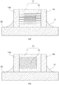
図1は、本発明の方法によって積層セラミックキャパシタ10が回路基板に実装された姿を示す断面図である。
FIG. 1 is a cross-sectional view showing a multilayer
本発明の積層セラミックキャパシタの回路基板実装構造及び方法は、内部電極12が設けられた誘電体シート11が積層され、該内部電極12と並列接続する外部端子電極14a、14bが両端部に設けられた積層セラミックキャパシタの回路基板への実装構造及び方法である。この方法において、前記回路基板20の表面に、積層セラミックキャパシタ10が実装されるランド(図示せず)を設け、該積層セラミックキャパシタ10の内部電極層12と前記回路基板20とが水平方向になるように配置して外部端子電極14a、14bとランドとを導電接続し、該外部端子電極14a、14bとランドとを導電接続する導電材15の高さ(Ts)は、積層セラミックキャパシタの厚さ(TMLCC)の1/3未満に設定される。
In the multilayer ceramic capacitor circuit board mounting structure and method of the present invention, a
図1に示すように、積層セラミックキャパシタ10は、誘電体層11と内部電極12とを交互に積層してなる素体13と、該素体13の両端部で内部電極を交互に並列接続している一対の外部電極14a、14bとから構成されている。
As shown in FIG. 1, a multilayer
該誘電体層11は、チタン酸バリウムなどを主成分とする強誘電体材料からなり、チタン酸バリウム以外の他の強誘電体材料を含んでもよい。
The
前記内部電極12は、金属ペーストを焼結させた金属薄膜からなり、該金属ペーストとしては、例えばNi、Pd、Ag−Pd、またはCuのような金属材料を主成分とするものが使われてもよい。
The
同様に、前記外部電極14a、14bは、Cu、Niなどのような金属材料から成り、その表面には、ハンダ付け漏れ性を良くするためにハンダメッキが実施されている。
Similarly, the
回路基板20の表面には、積層セラミックキャパシタを実装するためのランドが設けられる。該ランドは、回路基板20の内部のソルダレジストが露出し、該露出したソルダレジストの上面に導電材15がコーティングされ、積層セラミックキャパシタ10を実装するための部位である。回路基板20としては、多層回路基板、断層両面プリント基板などが挙げられ、これに限定されるものではない。
A land for mounting the multilayer ceramic capacitor is provided on the surface of the
積層セラミックキャパシタ10は、図2のように、幅(W)及び厚さ(T)が同一または類似の場合(図2a)と、幅が厚さより大きい場合(図2b)とがある。後者の場合は、意図せずとも、厚さが薄くて常に水平実装になるが、前者の場合には、水平実装と垂直実装とが無作為に行われるようになる。特に、積層セラミックキャパシタがリールのような包装体で包装される場合、積層セラミックキャパシタの内部電極が回路基板に水平方向に実装可能なように、一方向に整列するテーピングを施すことによって、幅(WMLCC)及び厚さ(TMLCC)が同一または類似の積層セラミックキャパシタの場合、水平実装の際、振動による騒音低減の効果をさらに高めることができる。ここで、積層セラミックキャパシタの幅及び厚さが同一または類似であるとは、0.75≦TMLCC/WMLCC≦1.25範囲内の場合をいう。
As shown in FIG. 2, the multilayer
ハンダなどの導電材15は、積層セラミックキャパシタ10と回路基板20との間の振動媒介体の役目をして、導電材15の高さを低くしながら基板への振動の伝達を低下させる。水平実装では、積層セラミックキャパシタ10の圧電性による縁部の振動のうち、上面の振動の伝達が導電材15の高さの低下とともに急に低下することになる。そのため、水平方向に実装する場合には、導電材15の高さの変化による振動騒音の減少幅が非常に大きくなる。
The
これに対して、垂直方向に実装する場合には、そのような効果が発生しないため、導電材15の高さの変化による振動騒音の減少幅は大きくない。
On the other hand, when mounting in the vertical direction, since such an effect does not occur, the reduction width of the vibration noise due to the change in the height of the
したがって、積層セラミックキャパシタによる騒音を低減させるためには、積層セラミックキャパシタ10は、内部電極12を基準として、回路基板20と水平方向になるように実装して導電材15の高さを減少させることが望ましい。
Therefore, in order to reduce the noise caused by the multilayer ceramic capacitor, the multilayer
図2に示す積層セラミックキャパシタの幅(W)及び長さ(L)によって、積層セラミックキャパシタは、0603(L×W=0.6mm×0.3mm)、1005、1608、2012、3216、3225などの大きさを有する。3216以上の大きい積層セラミックキャパシタの場合、その厚さに対して導電材の相対高さが低くても、該導電材の絶対量が多いので、振動騒音の低下効果を大きくするためには、該導電材の相対高さを1/4未満にすることが望ましい。 Depending on the width (W) and length (L) of the multilayer ceramic capacitor shown in FIG. 2, the multilayer ceramic capacitor is 0603 (L × W = 0.6 mm × 0.3 mm), 1005, 1608, 2012, 3216, 3225, etc. Have a size of In the case of a large multilayer ceramic capacitor of 3216 or more, even if the relative height of the conductive material is low with respect to its thickness, the absolute amount of the conductive material is large, so in order to increase the vibration noise reduction effect, It is desirable that the relative height of the conductive material be less than 1/4.
導電材15は、回路基板20と積層セラミックキャパシタとの間の電気的接続のために電気が導通する材料から成り、これは限定されるものではない。例えば、ハンダ付け(solder)を用いてもよい。
ランドパターン
The
Land pattern
図3は、本発明の一実施形態によるランドパターンを有する回路基板の平面図である。 FIG. 3 is a plan view of a circuit board having a land pattern according to an embodiment of the present invention.
図3に示すように、回路基板20に積層セラミックキャパシタが実装されるランド21、22が示されている。これらのランド21、22は、図1の積層セラミックキャパシタ10の外部端子電極14a、14bが設けられた個所に対応するように離間されて、回路基板の表面に複数個設けられる。これらのランドは、ソルダレシズトが覆われることなく露出した部分を意味する。
As shown in FIG. 3, lands 21 and 22 on which a multilayer ceramic capacitor is mounted on a
図3では、一実施形態として、四角形状のランドを2個設けた状態を示すが、これに限定されるものではない。ただ、前述のように、ランド21、22の表面にコーティングされる導電材15が振動騒音に影響を及ぼすが、ランド21、22が占める面積について、図4に示すように、一定の制限を設けることによって導電材の高さを減らすことができる。
Although FIG. 3 shows a state in which two rectangular lands are provided as an embodiment, the present invention is not limited to this. However, as described above, the
図4は、本発明の一実施形態によるランド21、22と積層セラミックキャパシタ10との間の幅及び長さの相関関係を示す模式図である。該積層セラミックキャパシタ10の幅をWMLCC、長さをLMLCCとして定義する。また、これらの離間された各ランド21、22のうちのいずれか一つのランド21の外側縁と他方のランド22の外側縁とを基準として、基板で占める幅をWLAND(a)、長さをLLAND(a)として定義する。このとき、WMLCC、LMLCC、WLAND(a)及びLLAND(a)の関係は、0<LLAND(a)/LMLCC≦1.2、0<WLAND(a)/WMLCC≦1.2であるのが望ましい。該範囲を外れる場合には、ランド21、22の表面にコーティングされる導電材の体積が大きくなるので、積層セラミックキャパシタ10で発生する振動を、回路基板10に伝達する作用が大きくなり、望ましくない。
FIG. 4 is a schematic diagram showing the correlation between the width and the length between the
図5は、本発明のさらに他の一実施形態によるランドパターンを有する回路基板の平面図である。 FIG. 5 is a plan view of a circuit board having a land pattern according to still another embodiment of the present invention.
図5には、回路基板20に、積層セラミックキャパシタが実装されるランド21a、21b、22a、22bが示されている。これらのランド21a、21b、22a、22bは、ハンダ付け量の減少のために、図1に示す積層セラミックキャパシタ10の外部端子電極14a、14bの各縁部に対応するように、それぞれ離間されて回路基板の表面に複数個設けられる。
FIG. 5 shows lands 21 a, 21 b, 22 a, and 22 b on which the multilayer ceramic capacitor is mounted on the
図5では、一実施形態として四角形状のランドを4個設けた状態を示すが、これに限定されるものではない。ただ、前述のように、ランド21a、21b、22a、22bの表面にコーティングされる導電材15が振動騒音に影響を及ぼすが、ランド21a、21b、22a、22bが占める面積には、図4に示すように、一定の制限がある。この場合、積層セラミックキャパシタ10の中央部の変位差が大きいことが予想されるため、複数個のランド21a、21b、21c、21dを分散させて、基板への振動の伝達を低減することができるようになる。
FIG. 5 shows a state in which four quadrangular lands are provided as an embodiment, but the present invention is not limited to this. However, as described above, the
図6は、本発明のさらに他の一実施形態によるランド21a、21b、22a、22bと積層セラミックキャパシタ10との間の幅、及び長さの相関関係を示す模式図である。該積層セラミックキャパシタ10の幅をWMLCC、長さをLMLCCとして定義し、互いに離間された各ランド21a、21b、22a、22bのうちのいずれか一側のランド21a、22aの外側縁と他側のランド21b、22bの外側縁とを基準として、基板で占める幅をWLAND(b)、一側のランド21a、21bと他側のランド22a、22bとが、基板で占める長さをLLAND(b)として定義する。このとき、WMLCC、LMLCC、WLAND(b)及びLLAND(b)の関係は、0<LLAND(b)/LMLCC≦1.2、0<WLAND(b)/WMLCC≦1.2であるのが望ましい。該範囲を外れる場合には、ランド21a、21b、22a、22bの表面にコーティングされる導電材の体積が大きくなるので、積層セラミックキャパシタ10で発生する振動を回路基板10に伝達する作用が大きくなり、望ましくない。
FIG. 6 is a schematic diagram showing the correlation between the width and the length between the
一方、この場合、外部端子電極14a、14bとランド21、22とを導電接続する導電材15の高さ(Ts)は、積層セラミックキャパシタの厚さ(TMLCC)の1/3未満とするのが望ましく、1/4未満とするのがさらに望ましい。ここで、積層セラミックキャパシタの外部電極端子の下辺部分のみに導電材が存在して、該導電材の高さがほとんど0の場合もある。積層セラミックキャパシタを水平方向に実装した状態で、導電材15の高さ(Ts)が減少するほど、該導電材15が回路基板20に振動を伝達する程度が、積層セラミックキャパシタを垂直方向に実装した状態よりも遥かに低くなるからである。
On the other hand, in this case, the height (T s ) of the
一方、本発明において、積層セラミックキャパシタは、水平方向にテーピングすると共に、幅(WMLCC)及び厚さ(TMLCC)が等しいものであってもよい。幅及び厚さが等しい場合、テーピング時に、一般的に同じ方向性を有することは難しいが、本発明においては、水平方向に一定にテーピングしたものを使うことによって、振動減少の効果を得ることができる。
積層セラミックキャパシタの包装体
On the other hand, in the present invention, the multilayer ceramic capacitor may be taped in the horizontal direction, and may have the same width (W MLCC ) and thickness (T MLCC ). When the width and thickness are equal, it is generally difficult to have the same directionality when taping. However, in the present invention, the effect of reducing vibrations can be obtained by using a tape that is uniformly taped in the horizontal direction. it can.
Multilayer ceramic capacitor packaging
前述のように、水平方向に一定にテーピングした積層セラミックキャパシタを提供するために、本発明は、水平方向に一定に整列した積層セラミックキャパシタの包装体を提供する。 As described above, in order to provide a monolithic ceramic capacitor taped uniformly in the horizontal direction, the present invention provides a package of monolithic ceramic capacitor that is uniformly aligned in the horizontal direction.
図7は、本発明の一実施形態による積層セラミックキャパシタが水平に配置されるように整列された積層セラミックキャパシタの包装体を示す。図8は、本発明のさらに他の一実施形態を示し、巻取られたリール形態の積層セラミックキャパシタの包装体を示す図である。 FIG. 7 illustrates a multilayer ceramic capacitor package that is arranged such that the multilayer ceramic capacitors are horizontally arranged according to an embodiment of the present invention. FIG. 8 shows still another embodiment of the present invention, and is a view showing a wound package of a multilayer ceramic capacitor in the form of a reel.
図7を参照すると、本実施形態の積層セラミックキャパシタの包装体40は、積層セラミックキャパシタ10が収納される収納部45が設けられた包装シート42を含む。
Referring to FIG. 7, the multilayer ceramic
該包装シート42の収納部45は、積層セラミックキャパシタ10と対応する形状を有し、該収納部45の底面を基準として内部電極12が水平に配置されるように移送部を通じて移動される。
The
積層セラミックキャパシタの包装体40は、前記収納部45の底面を基準として、前記内部電極12が水平となるように配置された積層セラミックキャパシタ10が収納された該包装シート42を覆う包装膜44をさらに含む。
The multilayer
図8は、リール形態に巻取られた形状の積層セラミックキャパシタの包装体を示す。この包装体は、図7に示す実施形態の積層セラミックキャパシタの包装体40が回収ロール(図示せず)によって、連続して巻取られて形成される。
積層セラミックキャパシタの水平方向整列方法
FIG. 8 shows a package of a multilayer ceramic capacitor having a shape wound in a reel form. This package is formed by continuously winding the
Method for horizontal alignment of multilayer ceramic capacitors
方向に、一定に整列した積層セラミックキャパシタの包装体40を提供するため、本発明は、幅及び厚さが同一または類似の積層セラミックキャパシタ10の水平方向整列方法を提供する。
In order to provide a monolithic
ここで、積層セラミックキャパシタの幅及び厚さが同一または類似であるとは、0.75≦TMLCC/WMLCC≦1.25範囲内の場合である。 Here, the width and thickness of the multilayer ceramic capacitor are the same or similar when the range is 0.75 ≦ T MLCC / W MLCC ≦ 1.25.
前述のように、幅及び厚さが同一または類似の積層セラミックキャパシタの圧電現象による振動騒音を大きく低減させるためには、積層セラミックキャパシタを回路基板に実装の際、積層セラミックキャパシタの内部電極面が回路基板面と水平に実装可能なように、包装体への収納過程において、積層セラミックキャパシタを水平方向に整列させることが必要である。 As described above, in order to greatly reduce vibration noise due to the piezoelectric phenomenon of multilayer ceramic capacitors having the same or similar width and thickness, when the multilayer ceramic capacitor is mounted on a circuit board, the internal electrode surface of the multilayer ceramic capacitor is It is necessary to align the multilayer ceramic capacitors in the horizontal direction in the process of being housed in the package so that they can be mounted horizontally with the circuit board surface.
このため、本発明では、磁気力を用いる整列方法を提供する。図9に示すように、積層セラミックキャパシタ10に磁石を近づけると、磁気抵抗が減るように、内部電極導体が、図9(a)及び(b)に示すような積層セラミックキャパシタ10、10’の方向では、磁石に吸着される。しかし、図9(c)に示すような内部電極導体の積層方向から磁石を近づける積層セラミックキャパシタ10’’の方向では、磁石に吸着しないという性質を利用する。
For this reason, the present invention provides an alignment method using magnetic force. As shown in FIG. 9, the internal electrode conductors of the multilayer
そのような性質を用いて、幅及び厚さが同一または類似の積層セラミックキヤパシタ10を包装体で水平方向に収納するため、移送過程中に、図10のように、磁石を側方に配置して積層セラミックキャパシタ10を水平に整列させる。
Using such a property, in order to accommodate the laminated
この場合、図9(c)に示す積層セラミックキャパシタ10"は、磁気力によって、内部電極面が移送部100の移送方向に回転して整列するようになる。
In this case, in the multilayer
しかし、図11に示すように、移送過程中、図9(b)に示す積層セラミックキャパシタ10’のような状態(積層方向が磁石に向いている)に配列される場合が発生する。これは、図12に示すように、移送部100に所定の間隔を有する一対のガイド110を設けることによって解決することができる。
However, as shown in FIG. 11, during the transfer process, there is a case where the multilayer
この場合、該一対のガイド部110間の間隔gは、積層セラミックキャパシタの幅をWMLCC、厚さをTMLCC、長さをLMLCCとして定義すると、下式、
√(W2 MLCC+T2 MLCC)<g<min〔√(L2 MLCC+T2 MLCC),√(L2 MLCC+W2 MLCC)〕
を満足する。
In this case, an interval g between the pair of
√ (W 2 MLCC + T 2 MLCC ) <g <min [√ (L 2 MLCC + T 2 MLCC ), √ (L 2 MLCC + W 2 MLCC )]
Satisfied.
以下では、本発明の好適な実施形態を導出するための試験例について説明することにする。 Hereinafter, a test example for deriving a preferred embodiment of the present invention will be described.
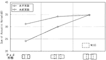
試験例1:積層セラミックキャパシタを回路基板上に水平実装する場合と垂直実装する場合について、導電材の高さが振動騒音に及ぶ影響の評価 Test example 1: Evaluation of the effect of the height of the conductive material on vibration noise when the multilayer ceramic capacitor is mounted horizontally and vertically on the circuit board
まず、積層セラミックキャパシタが水平実装された場合と垂直実装された場合について、ハンダの高さが振動騒音に及ぶ影響を確認するために、マイクロドリルを用いて、ハンダの高さを次第に低くしながら、振動による騒音を測定した。 First, in order to confirm the effect of the height of the solder on the vibration noise when the multilayer ceramic capacitor is mounted horizontally and vertically, using a micro drill, while gradually reducing the height of the solder The noise due to vibration was measured.
図13は、積層セラミックキャパシタを回路基板上に水平実装する場合(a)と垂直実装する場合(b)とを示し、図14はその測定結果をグラフとして示す。 FIG. 13 shows a case where the multilayer ceramic capacitor is horizontally mounted on the circuit board (a) and a case where it is vertically mounted (b), and FIG. 14 shows the measurement result as a graph.
図14に示すように、ハンダの高さが低いほど振動騒音が減少することが認められる。特に、垂直実装する場合よりも水平実装する場合のほうが、振動騒音の変化幅が大きいという事実が分かつた。 As shown in FIG. 14, it is recognized that the vibration noise decreases as the solder height is lower. In particular, it was found that the variation width of vibration noise is larger in the case of horizontal mounting than in the case of vertical mounting.
このような事実は、ハンダなどの導電材は、積層セラミックキャパシタと回路基板との間の振動媒介体としての役目を有し、該導電材の高さが低くなるにつれて基板への振動の伝達が低下するが、水平実装では、積層セラミックキャパシタの圧電性による縁部の振動の中で上面の振動の伝達が、該導電材の高さの低下とともに急に低下することで生じる。そのため、水平方向に実装する場合には、導電材の高さの変化による振動騒音の減少幅が非常に大きくなる一方、垂直方向に実装する場合には、該効果が発生しないので導電材の高さの変化による振動騒音の減少幅が大きくない。そのため、積層セラミックキャパシタは、内部電極を基準として回路基板と水平方向になるように実装し、ハンダ付け量(高さ)を少なくするのが騒音を減らすのに望ましい、という事実が認められる。 Such a fact indicates that a conductive material such as solder serves as a vibration medium between the multilayer ceramic capacitor and the circuit board, and as the height of the conductive material decreases, transmission of vibration to the board is reduced. However, in horizontal mounting, the vibration of the upper surface in the vibration of the edge due to the piezoelectricity of the multilayer ceramic capacitor is caused by abruptly decreasing as the height of the conductive material decreases. Therefore, when mounting in the horizontal direction, the reduction in vibration noise due to changes in the height of the conductive material becomes very large, whereas when mounting in the vertical direction, this effect does not occur, so the height of the conductive material is high. The reduction of vibration noise due to the change in height is not large. Therefore, it is recognized that the multilayer ceramic capacitor is preferably mounted in the horizontal direction with respect to the circuit board with the internal electrode as a reference, and it is desirable to reduce the soldering amount (height) in order to reduce noise.
試験例2:積層セラミックキャパシタを回路基板上に水平実装する場合と垂直実装する場合について、ランドの大きさが振動騒音に及ぶ影響の評価 Test example 2: Evaluation of the effect of land size on vibration noise when multilayer ceramic capacitors are mounted horizontally and vertically on a circuit board
試験例1において、ハンダの高さによる振動騒音の変化結果に基づいて、追加的にランドの大きさによる振動騒音を測定し、これを図15のグラフとして示した。 In Test Example 1, vibration noise due to the size of the land was additionally measured based on the change result of the vibration noise due to the height of the solder, and this was shown as a graph in FIG.
図15から理解されるように、ランドの大きさを小さくするほど導電材の高さが低くなり、基板への振動が伝達されにくくなり、振動騒音が減少することが認められた。また、同様に、水平実装する場合、振動騒音が大幅に低減することが認められた。 As understood from FIG. 15, it was recognized that the smaller the size of the land, the lower the height of the conductive material, making it difficult to transmit the vibration to the substrate and reducing the vibration noise. Similarly, it was found that vibration noise was greatly reduced when mounted horizontally.
一方、図2の積層セラミックキャパシタの幅(W)及び長さ(L)によって、積層セラミックキャパシタは、0603(L×W=0.6mm×0.3mm)、1005、1608、2012、3216、3225などの大きさを有する場合がある。このような大きさの積層セラミックキャパシタに対して水平実装すると共に、ランドの大きさを小さくした場合、振動騒音が大幅に低下する効果が認められた。しかしながら、3216以上の大きさの積層セラミックキャパシタの場合は、積層セラミックキャパシタの厚さに対して導電材の相対高さが低くても、該導電材の絶対量が多いので、振動騒音の低下効果を大きくするためには、該導電材の相対高さをさらに低くしなければならないことも認められた。 On the other hand, depending on the width (W) and length (L) of the multilayer ceramic capacitor of FIG. 2, the multilayer ceramic capacitor is 0603 (L × W = 0.6 mm × 0.3 mm), 1005, 1608, 2012, 3216, 3225. And so on. It was confirmed that when the size of the land was reduced while mounting horizontally on the multilayer ceramic capacitor of such a size, the vibration noise was greatly reduced. However, in the case of a multilayer ceramic capacitor having a size of 3216 or more, even if the relative height of the conductive material is low with respect to the thickness of the multilayer ceramic capacitor, the absolute amount of the conductive material is large. It was also recognized that the relative height of the conductive material had to be further reduced in order to increase the thickness.
今回開示された実施の形態はすべての点で例示であって、制限的なものではないと考えられるべきである。本発明の範囲は、前記した実施の形態の説明ではなくて特許請求の範囲によって示され、特許請求の範囲と均等の意味及び範囲内でのすべての変更が含まれることが意図される。 The embodiment disclosed this time is to be considered as illustrative in all points and not restrictive. The scope of the present invention is shown not by the above description of the embodiments but by the scope of claims, and is intended to include all modifications within the meaning and scope equivalent to the scope of claims.
10 積層セラミックキャパシタ
11 誘電体シート
12 内部電極
14a、14b 外部端子電極
15 導電材
20 回路基板
DESCRIPTION OF
Claims (27)
前記積層セラミックキャパシタの内部電極層と前記回路基板とは、互いに水平方向になるように配置されて、前記外部端子電極と前記回路基板のランドとを導電接続し、
前記外部端子電極と前記ランドとを導電接続する導電材の高さ(Ts)は、前記積層セラミックキャパシタの厚さ(TMLCC)の1/3未満である積層セラミックキャパシタの回路基板実装構造。 A dielectric sheet provided with an internal electrode is laminated, and an external terminal electrode connected in parallel with the internal electrode is a mounting structure on a circuit board of a multilayer ceramic capacitor provided at both ends,
The internal electrode layer of the multilayer ceramic capacitor and the circuit board are disposed so as to be in a horizontal direction, and conductively connect the external terminal electrode and the land of the circuit board,
A circuit board mounting structure of a multilayer ceramic capacitor, wherein a height (T s ) of a conductive material that conductively connects the external terminal electrode and the land is less than 1/3 of a thickness (T MLCC ) of the multilayer ceramic capacitor.
前記積層セラミックキャパシタの内部電極層と前記回路基板が互いに水平方向になるように配置されて、前記外部端子電極と前記回路基板のランドとを導電接続し、
前記外部端子電極と前記ランドとを導電接続する導電材の高さ(Ts)は、前記積層セラミックキャパシタの厚さ(TMLCC)の1/3未満である積層セラミックキャパシタの回路基板実装方法。 A method of mounting a multilayer ceramic capacitor on a circuit board in which dielectric sheets provided with internal electrodes are laminated and external terminal electrodes connected in parallel with the internal electrodes are provided at both ends,
The internal electrode layer of the multilayer ceramic capacitor and the circuit board are arranged so as to be horizontal with each other, and the external terminal electrode and the land of the circuit board are conductively connected,
A method for mounting a multilayer ceramic capacitor on a circuit board, wherein a height (T s ) of a conductive material for conductively connecting the external terminal electrode and the land is less than 1/3 of a thickness (T MLCC ) of the multilayer ceramic capacitor.
前記回路基板の表面に前記積層セラミックキャパシタが実装されるランドを設け、
前記積層セラミックキャパシタの内部電極層と前記回路基板が互いに水平方向になるように配置して前記外部端子電極と前記回路基板のランドとを導電接続し、
前記ランドは、前記積層セラミックキャパシタの外部端子電極の設けられた個所に対応するように離間されて前記回路基板の表面に複数個設けられ、
前記積層セラミックキャパシタの幅をWMLCC、長さをLMLCCとして定義し、前記離間された各ランドのうちのいずれか一方のランドの外側縁と他方のランドの外側縁とを基準として、基板で占める幅をWLAND(a)、長さをLLAND(a)として定義すると、
WMLCC、LMLCC、WLAND(a)及びLLAND(a)の関係は、下式、
0<LLAND(a)/LMLCC≦1.2
0<WLAND(a)/MLCCC≦1.2
を満たす積層セラミックキャパシタの回路基板実装方法。 A method of mounting a multilayer ceramic capacitor on a circuit board in which dielectric sheets provided with internal electrodes are laminated and external terminal electrodes connected in parallel with the internal electrodes are provided at both ends,
Provide a land on which the multilayer ceramic capacitor is mounted on the surface of the circuit board,
The internal electrode layer of the multilayer ceramic capacitor and the circuit board are arranged in a horizontal direction to electrically connect the external terminal electrode and the land of the circuit board,
A plurality of the lands are provided on the surface of the circuit board so as to correspond to the locations where the external terminal electrodes of the multilayer ceramic capacitor are provided,
The width of the multilayer ceramic capacitor W MLCC, define the length as L MLCC, as any reference to the outer edge of the outer edge and the other of the land of one of the lands of the land where the spaced, the substrate If we define the occupying width as W LAND (a) and the length as L LAND (a) ,
The relationship between W MLCC , L MLCC , W LAND (a) and L LAND (a) is
0 <L LAND (a) / L MLCC ≦ 1.2
0 <W LAND (a) / M LCCC ≦ 1.2
Circuit board mounting method of multilayer ceramic capacitor satisfying
前記回路基板の表面に前記積層セラミックキャパシタが実装されるランドを設け、
前記積層セラミックキャパシタの内部電極層と前記回路基板とが互いに水平方向になるように配置して前記外部端子電極と前記回路基板のランドとを導電接続し、
前記ランドは、ハンダ付け量の減少のために、前記積層セラミックキャパシタの外部端子電極の設けられた縁部に対応するように離間されて前記回路基板の表面に複数個設けられる、積層セラミックキャパシタの回路基板実装方法。 A method of mounting a multilayer ceramic capacitor on a circuit board in which dielectric sheets provided with internal electrodes are laminated and external terminal electrodes connected in parallel with the internal electrodes are provided at both ends,
Provide a land on which the multilayer ceramic capacitor is mounted on the surface of the circuit board,
The internal electrode layer of the multilayer ceramic capacitor and the circuit board are arranged so as to be in a horizontal direction to electrically connect the external terminal electrode and the land of the circuit board,
In the multilayer ceramic capacitor, a plurality of the lands are provided on the surface of the circuit board so as to be spaced apart from each other so as to correspond to an edge provided with the external terminal electrode of the multilayer ceramic capacitor in order to reduce a soldering amount. Circuit board mounting method.
WMLCC、LMLCC、WLAND(b)及びLLAND(b)の関係は、下式、
0<LLAND(b)/LMLCC≦1.2
0<WLAND(b)/WMLCC≦1.2
を満たす請求項12に記載の積層セラミックキャパシタの回路基板実装方法。 The width of the multilayer ceramic capacitor is defined as W MLCC , the length is defined as L MLCC , and the width occupied by the substrate based on the outer edge of one of the separated lands and the outer edge of the other land Is defined as W LAND (b) and the length as L LAND (b) .
The relationship between W MLCC , L MLCC , W LAND (b) and L LAND (b) is
0 <L LAND (b) / L MLCC ≦ 1.2
0 <W LAND (b) / W MLCC ≦ 1.2
The circuit board mounting method of the multilayer ceramic capacitor according to claim 12, wherein
前記ランドパターンは、前記積層セラミックキャパシタの外部端子電極の設けられた個所に対応するように離間されて前記回路基板の表面に複数個設けられ、
前記積層セラミックキャパシタの幅をWMLCC、長さをLMLCCとして定義し、前記離間された各ランドのうちのいずれか一方のランドの外側縁と他方のランドの外側縁とを基準として、基板で占める幅をWLAND(a)、長さをLLAND(a)として定義すると、
WMLCC、LMLCC、WLAND(a)及びLLAND(a)の関係は、下式、
0<LLAND(a)/LMLCC≦1.2
0<WLAND(a)/WMLCC≦1.2
を満たす回路基板上のランドパターン。 A land pattern on a circuit board on which a multilayer ceramic capacitor in which dielectric sheets provided with internal electrodes are stacked and external terminal electrodes connected in parallel with the internal electrodes are provided at both ends is mounted,
A plurality of the land patterns are provided on the surface of the circuit board so as to correspond to locations where the external terminal electrodes of the multilayer ceramic capacitor are provided,
The width of the multilayer ceramic capacitor W MLCC, define the length as L MLCC, as any reference to the outer edge of the outer edge and the other of the land of one of the lands of the land where the spaced, the substrate If we define the occupying width as W LAND (a) and the length as L LAND (a) ,
The relationship between W MLCC , L MLCC , W LAND (a) and L LAND (a) is
0 <L LAND (a) / L MLCC ≦ 1.2
0 <W LAND (a) / W MLCC ≦ 1.2
Land pattern on the circuit board that meets the requirements.
前記ランドパターンは、ハンダ付け量の減少のために、前記積層セラミックキャパシタの外部端子電極の設けられた縁部に対応するように離間されて前記回路基板の表面に複数個設けられ、
前記積層セラミックキャパシタの幅をWMLCC、長さをLMLCCとして定義し、前記離間された各ランドのうちのいずれか一方の外側縁と他方のランドの外側縁とを基準として、基板で占める幅をWLAND(b)、長さをLLAND(b)として定義すると、
WMLCC、LMLCC、WLAND(b)及びLLAND(b)の関係は、下式、
0<LLAND(b)/LMLCC≦1.2
0<WLAND(b)/WMLCC≦1.2
を満たす回路基板上のランドパターン。 A land pattern on a circuit board on which a multilayer ceramic capacitor in which dielectric sheets provided with internal electrodes are stacked and external terminal electrodes connected in parallel with the internal electrodes are provided at both ends is mounted,
A plurality of the land patterns are provided on the surface of the circuit board so as to correspond to the edges provided with the external terminal electrodes of the multilayer ceramic capacitor in order to reduce the amount of soldering,
The width of the multilayer ceramic capacitor is defined as W MLCC , the length is defined as L MLCC , and the width occupied by the substrate based on the outer edge of one of the separated lands and the outer edge of the other land Is defined as W LAND (b) and the length as L LAND (b) .
The relationship between W MLCC, L MLCC , W LAND (b) and L LAND (b) is
0 <L LAND (b) / L MLCC ≦ 1.2
0 <W LAND (b) / W MLCC ≦ 1.2
Land pattern on the circuit board that meets the requirements.
前記積層セラミックキャパシタが収納される収納部が設けられる包装シートと、を含み、
前記内部電極は、前記収納部の底面を基準に水平に配置されるように整列され、前記積層セラミックキャパシタが整列された包装シートがリール形態に巻き取られた積層セラミックキャパシタの包装体。 A multilayer ceramic capacitor in which dielectric sheets provided with internal electrodes are laminated, and external terminal electrodes connected in parallel with the internal electrodes are provided at both ends,
And a packaging sheet provided with a storage unit in which the multilayer ceramic capacitor is stored,
The package of multilayer ceramic capacitors in which the internal electrodes are aligned so as to be horizontally disposed with reference to the bottom surface of the storage unit, and a package sheet in which the multilayer ceramic capacitors are aligned is wound in a reel form.
前記積層セラミックキャパシタを移送部に実装して、該積層セラミックキャパシタが連続して移送されるようにするステップと、
前記移送部によって移送される前記積層セラミックキャパシタに磁場を印加し、内部電極層が該磁場及び磁気抵抗が減る方向に整列されるようにするステップと、を含む積層セラミックキャパシタの水平方向整列方法。 A method for horizontally aligning multilayer ceramic capacitors having the same or similar width (W MLCC ) and thickness (T MLCC ),
Mounting the multilayer ceramic capacitor on a transfer unit so that the multilayer ceramic capacitor is continuously transferred; and
Applying a magnetic field to the multilayer ceramic capacitor transferred by the transfer unit so that the internal electrode layers are aligned in a direction in which the magnetic field and magnetoresistance decrease.
√(W2 MLCC+T2 MLCC)<g<min〔√(L2 MLCC+T2 MLCC),√(L2 MLCC+W2 MLCC)〕
を満足する請求項26に記載の積層セラミックキャパシタの水平方向整列方法。 The gap g between the pair of guide portions is defined by the following equation, when the width of the multilayer ceramic capacitor is defined as W MLCC , the thickness is TMLCC, and the length is L MLCC :
√ (W 2 MLCC + T 2 MLCC ) <g <min [√ (L 2 MLCC + T 2 MLCC ), √ (L 2 MLCC + W 2 MLCC )]
27. The method for horizontally aligning multilayer ceramic capacitors according to claim 26, wherein:
Applications Claiming Priority (2)
| Application Number | Priority Date | Filing Date | Title |
|---|---|---|---|
| KR10-2010-0131716 | 2010-12-21 | ||
| KR1020100131716A KR101058697B1 (en) | 2010-12-21 | 2010-12-21 | Mounting structure of ciruit board having thereon multi-layered ceramic capacitor, method thereof, land pattern of circuit board for the same, packing unit for multi-layered ceramic capacitor taped horizontally and aligning method thereof |
Related Child Applications (2)
| Application Number | Title | Priority Date | Filing Date |
|---|---|---|---|
| JP2012142456A Division JP2012216864A (en) | 2010-12-21 | 2012-06-25 | Mounting structure and method of circuit board for multi-layered ceramic capacitor, land pattern of circuit board, packing unit for multi-layered ceramic capacitor, and aligning method |
| JP2013102898A Division JP2013153231A (en) | 2010-12-21 | 2013-05-15 | Circuit board mounting structure of multi-layered ceramic capacitor, method thereof, land pattern of circuit board, packing unit for multi-layered ceramic capacitor and aligning method |
Publications (2)
| Publication Number | Publication Date |
|---|---|
| JP2012134498A true JP2012134498A (en) | 2012-07-12 |
| JP2012134498A5 JP2012134498A5 (en) | 2012-08-23 |
Family
ID=44933636
Family Applications (3)
| Application Number | Title | Priority Date | Filing Date |
|---|---|---|---|
| JP2011276870A Pending JP2012134498A (en) | 2010-12-21 | 2011-12-19 | Circuit board mount structure and method for multilayer ceramic capacitor, land pattern of circuit board, and package and alignment method for multilayer ceramic capacitor |
| JP2012142456A Pending JP2012216864A (en) | 2010-12-21 | 2012-06-25 | Mounting structure and method of circuit board for multi-layered ceramic capacitor, land pattern of circuit board, packing unit for multi-layered ceramic capacitor, and aligning method |
| JP2013102898A Pending JP2013153231A (en) | 2010-12-21 | 2013-05-15 | Circuit board mounting structure of multi-layered ceramic capacitor, method thereof, land pattern of circuit board, packing unit for multi-layered ceramic capacitor and aligning method |
Family Applications After (2)
| Application Number | Title | Priority Date | Filing Date |
|---|---|---|---|
| JP2012142456A Pending JP2012216864A (en) | 2010-12-21 | 2012-06-25 | Mounting structure and method of circuit board for multi-layered ceramic capacitor, land pattern of circuit board, packing unit for multi-layered ceramic capacitor, and aligning method |
| JP2013102898A Pending JP2013153231A (en) | 2010-12-21 | 2013-05-15 | Circuit board mounting structure of multi-layered ceramic capacitor, method thereof, land pattern of circuit board, packing unit for multi-layered ceramic capacitor and aligning method |
Country Status (5)
| Country | Link |
|---|---|
| US (2) | US20120152604A1 (en) |
| JP (3) | JP2012134498A (en) |
| KR (1) | KR101058697B1 (en) |
| CN (3) | CN102548213B (en) |
| TW (2) | TWI534844B (en) |
Cited By (19)
| Publication number | Priority date | Publication date | Assignee | Title |
|---|---|---|---|---|
| JP2013235928A (en) * | 2012-05-08 | 2013-11-21 | Murata Mfg Co Ltd | Ceramic electronic component and electronic device |
| JP2014033097A (en) * | 2012-08-03 | 2014-02-20 | Tdk Corp | Multilayer ceramic capacitor |
| JP2014096555A (en) * | 2012-11-09 | 2014-05-22 | Samsung Electro-Mechanics Co Ltd | Multilayer ceramic capacitor, circuit board mounting structure of multilayer ceramic capacitor and package of multilayer ceramic capacitor |
| JP2014096554A (en) * | 2012-11-09 | 2014-05-22 | Samsung Electro-Mechanics Co Ltd | Multilayer ceramic capacitor, circuit board mounting structure of multilayer ceramic capacitor and package of multilayer ceramic capacitor |
| JP2014099589A (en) * | 2012-10-19 | 2014-05-29 | Murata Mfg Co Ltd | Method of manufacturing mounting substrate on which multilayer ceramic capacitors are mounted and mounting structure body |
| JP2014103371A (en) * | 2012-11-20 | 2014-06-05 | Samsung Electro-Mechanics Co Ltd | Multilayer ceramic capacitor, circuit board packaging structure of multilayer ceramic capacitor, and packaging body of multilayer ceramic capacitor |
| JP2014132631A (en) * | 2013-01-02 | 2014-07-17 | Samsung Electro-Mechanics Co Ltd | Laminated ceramic capacitor and mounting board of the same |
| KR20140092107A (en) * | 2013-01-15 | 2014-07-23 | 삼성전기주식회사 | Multi-layered capacitor and circuit board mounted multi-layered capacitor |
| JP2015037182A (en) * | 2013-08-14 | 2015-02-23 | サムソン エレクトロ−メカニックス カンパニーリミテッド. | Mounting board for multilayer ceramic capacitor |
| JP2015092625A (en) * | 2015-01-16 | 2015-05-14 | 株式会社村田製作所 | Method for discriminating direction of multilayer ceramic capacitor, direction discriminating device for multilayer ceramic capacitor, and method of manufacturing multilayer ceramic capacitor |
| KR20150084078A (en) * | 2014-01-10 | 2015-07-22 | 삼성전기주식회사 | Multi-layered ceramic capacitor and board having the same mounted thereon |
| JP2015147618A (en) * | 2014-01-10 | 2015-08-20 | 株式会社村田製作所 | Manufacturing device of taping electronic component series, manufacturing method of taping electronic component series, conveyance device of electronic component, conveyance method of electronic component, and taping electronic component series |
| JP2016018985A (en) * | 2014-07-07 | 2016-02-01 | サムソン エレクトロ−メカニックス カンパニーリミテッド. | Laminated ceramic capacitor, manufacturing method of laminated ceramic capacitor, and mounting substrate for laminated ceramic capacitor |
| JP2016213341A (en) * | 2015-05-11 | 2016-12-15 | 株式会社村田製作所 | Posture discrimination method of multilayer ceramic capacitor, posture discrimination device of multilayer ceramic capacitor, manufacturing method for multilayer ceramic capacitor, and multilayer ceramic capacitor series |
| JP2017017212A (en) * | 2015-07-02 | 2017-01-19 | 株式会社村田製作所 | Electronic component conveyance device |
| JP2018088534A (en) * | 2012-07-20 | 2018-06-07 | サムソン エレクトロ−メカニックス カンパニーリミテッド. | Laminated chip electronic component, board for mounting the same, and packing unit thereof |
| US10141111B2 (en) | 2012-12-28 | 2018-11-27 | Murata Manufacturing Co., Ltd. | Method of manufacturing stacked ceramic capacitor including identifying direction of stacking in stacked ceramic capacitor |
| WO2022186190A1 (en) * | 2021-03-02 | 2022-09-09 | 京セラ株式会社 | Method for aligning laminated component, and method for producing laminated ceramic electronic component |
| WO2024009788A1 (en) * | 2022-07-05 | 2024-01-11 | 太陽誘電株式会社 | Laminated ceramic capacitor, package, and circuit board |
Families Citing this family (43)
| Publication number | Priority date | Publication date | Assignee | Title |
|---|---|---|---|---|
| KR101548773B1 (en) * | 2011-08-22 | 2015-08-31 | 삼성전기주식회사 | Mounting structure of ciruit board having thereon multi-layered ceramic capacitor |
| KR101309326B1 (en) * | 2012-05-30 | 2013-09-16 | 삼성전기주식회사 | Laminated chip electronic component, board for mounting the same, packing unit thereof |
| KR101309479B1 (en) | 2012-05-30 | 2013-09-23 | 삼성전기주식회사 | Laminated chip electronic component, board for mounting the same, packing unit thereof |
| CN103489639B (en) | 2012-06-12 | 2016-07-06 | 株式会社村田制作所 | Cascade capacitor |
| US8934215B2 (en) * | 2012-07-20 | 2015-01-13 | Samsung Electro-Mechanics Co., Ltd | Laminated chip electronic component, board for mounting the same, and packing unit thereof |
| US9805867B2 (en) | 2012-09-19 | 2017-10-31 | Apple Inc. | Acoustically quiet capacitors |
| KR101474065B1 (en) * | 2012-09-27 | 2014-12-17 | 삼성전기주식회사 | Laminated chip electronic component, board for mounting the same, packing unit thereof |
| KR101376843B1 (en) * | 2012-11-29 | 2014-03-20 | 삼성전기주식회사 | Multi-layered ceramic capacitor, mounting structure of circuit having thereon multi-layered ceramic capacitor and packing unit for multi-layered ceramic capacitor |
| KR101452054B1 (en) * | 2012-12-03 | 2014-10-22 | 삼성전기주식회사 | Multi-layered ceramic capacitor and board for mounting the same |
| KR101452067B1 (en) * | 2012-12-14 | 2014-10-16 | 삼성전기주식회사 | Multi-layered ceramic capacitor and board for mounting the same |
| KR20140080019A (en) * | 2012-12-20 | 2014-06-30 | 삼성전기주식회사 | Multi-layered ceramic capacitor and mounting circuit having thereon multi-layered ceramic capacitor |
| KR101452079B1 (en) * | 2012-12-28 | 2014-10-16 | 삼성전기주식회사 | Embedded multilayer capacitor and print circuit board having embedded multilayer capacitor |
| KR101548793B1 (en) * | 2013-01-14 | 2015-08-31 | 삼성전기주식회사 | Multi-layered ceramic capacitor, mounting circuit thereof and manufacturing method of the same |
| US9287049B2 (en) | 2013-02-01 | 2016-03-15 | Apple Inc. | Low acoustic noise capacitors |
| KR101412940B1 (en) * | 2013-03-29 | 2014-06-26 | 삼성전기주식회사 | Multi-layered ceramic capacitor and mounting circuit of multi-layered ceramic capacitor |
| KR101496816B1 (en) | 2013-04-26 | 2015-02-27 | 삼성전기주식회사 | Multi-layered ceramic electronic part and board for mounting the same |
| KR101565643B1 (en) | 2013-04-30 | 2015-11-03 | 삼성전기주식회사 | Multi-layered ceramic electronic part and board for mounting the same |
| JP6798766B2 (en) * | 2013-06-19 | 2020-12-09 | 太陽誘電株式会社 | Multilayer ceramic capacitors |
| KR101496813B1 (en) * | 2013-07-05 | 2015-02-27 | 삼성전기주식회사 | Multi-layered ceramic capacitor, mounting circuit board thereof and manufacturing method the same |
| KR101434107B1 (en) | 2013-07-17 | 2014-08-25 | 삼성전기주식회사 | Embedded multi-layered ceramic capacitor, method of manufacturing the same and manufacturing method of embedded circuit |
| KR101434108B1 (en) | 2013-07-22 | 2014-08-25 | 삼성전기주식회사 | Multi-layered ceramic capacitor, mounting circuit board thereof and manufacturing method the same |
| KR101496814B1 (en) * | 2013-07-29 | 2015-02-27 | 삼성전기주식회사 | Multilayered ceramic capacitor, the method of the same and board for mounting the same |
| KR101532141B1 (en) | 2013-09-17 | 2015-06-26 | 삼성전기주식회사 | Multi-layered ceramic electronic part and board for mounting the same |
| JP5790817B2 (en) | 2013-11-05 | 2015-10-07 | 株式会社村田製作所 | Capacitor, capacitor mounting structure and taping electronic component series |
| DE112014005686T5 (en) * | 2013-12-13 | 2016-09-15 | Mitsubishi Heavy Industries Automotive Thermal Systems Co., Ltd. | Mounting structure for electronic component |
| JP5958479B2 (en) * | 2014-01-31 | 2016-08-02 | 株式会社村田製作所 | Electronic component mounting structure |
| KR101630037B1 (en) | 2014-05-08 | 2016-06-13 | 삼성전기주식회사 | Multi-layered ceramic capacitor, array-type multi-layered ceramic capacitor, manufacturing method for the same and board having the same mounted thereon |
| JP2015228482A (en) * | 2014-05-09 | 2015-12-17 | 株式会社村田製作所 | Mounting structure of multilayer ceramic electronic component |
| KR20150135909A (en) * | 2014-05-26 | 2015-12-04 | 삼성전기주식회사 | Composite electronic component, manufacturing method thereof, board for mounting the same and packing unit thereof |
| US10204737B2 (en) | 2014-06-11 | 2019-02-12 | Avx Corporation | Low noise capacitors |
| US20150364253A1 (en) * | 2014-06-12 | 2015-12-17 | Apple Inc. | Heel fillet capacitor with noise reduction |
| JP2016040819A (en) | 2014-08-13 | 2016-03-24 | 株式会社村田製作所 | Multilayer ceramic capacitor, multilayer ceramic capacitor couple including the same, and multilayer ceramic capacitor assembly |
| JP2016040816A (en) * | 2014-08-13 | 2016-03-24 | 株式会社村田製作所 | Multilayer ceramic capacitor, multilayer ceramic capacitor couple including the same, and multilayer ceramic capacitor assembly |
| JP2016040817A (en) | 2014-08-13 | 2016-03-24 | 株式会社村田製作所 | Multilayer ceramic capacitor, multilayer ceramic capacitor couple including the same, and multilayer ceramic capacitor assembly |
| JP6554932B2 (en) | 2015-06-16 | 2019-08-07 | 株式会社村田製作所 | Electronic component conveying apparatus and taping electronic component series manufacturing method |
| JP6520441B2 (en) * | 2015-06-16 | 2019-05-29 | 株式会社村田製作所 | Electronic component conveying apparatus and method of manufacturing taping electronic component train |
| JP6512139B2 (en) * | 2016-03-04 | 2019-05-15 | 株式会社村田製作所 | Electronic component mounting structure and method of manufacturing the electronic component |
| US10504655B2 (en) * | 2016-12-22 | 2019-12-10 | Samsung Electro-Mechanics Co., Ltd. | Composite electronic component and board having the same |
| JP6798528B2 (en) * | 2018-05-28 | 2020-12-09 | 株式会社村田製作所 | How to align chip parts |
| CN112750620A (en) * | 2019-05-22 | 2021-05-04 | 何俊建 | Anti-vibration capacitor and use method thereof |
| KR20220090988A (en) * | 2020-12-23 | 2022-06-30 | 삼성전기주식회사 | Multi-layer ceramic electronic component and board for mounting the same |
| CN114666998A (en) * | 2020-12-23 | 2022-06-24 | 杭州海康威视数字技术股份有限公司 | Method for manufacturing on-board capacitor and printed circuit board |
| WO2023032591A1 (en) * | 2021-08-30 | 2023-03-09 | 京セラ株式会社 | Alignment method for laminated component, and method for manufacturing laminated ceramic electronic component using said alignment method |
Citations (7)
| Publication number | Priority date | Publication date | Assignee | Title |
|---|---|---|---|---|
| JPS6352770U (en) * | 1986-09-25 | 1988-04-09 | ||
| JP2003282332A (en) * | 2002-03-25 | 2003-10-03 | Murata Mfg Co Ltd | Ceramic electronic component and method of manufacturing the ceramic electronic component |
| JP2004193352A (en) * | 2002-12-11 | 2004-07-08 | Taiyo Yuden Co Ltd | Layered capacitor and its mounted product |
| JP2004259991A (en) * | 2003-02-26 | 2004-09-16 | Kyocera Corp | Laminated ceramic component |
| JP2005217136A (en) * | 2004-01-29 | 2005-08-11 | Tdk Corp | Aligning method and device of lamination electronic component |
| WO2007007677A1 (en) * | 2005-07-07 | 2007-01-18 | Murata Manufacturing Co., Ltd. | Electronic component, electronic component mounted structure, and process for producing electronic component |
| JP2009164446A (en) * | 2008-01-09 | 2009-07-23 | Panasonic Corp | Multilayer ceramic capacitor and method of manufacturing the same |
Family Cites Families (28)
| Publication number | Priority date | Publication date | Assignee | Title |
|---|---|---|---|---|
| US3785895A (en) * | 1969-09-25 | 1974-01-15 | Vitta Corp | Tape transfer of sinterable conductive,semiconductive or insulating patterns to electronic component substrates |
| JPS5599795A (en) * | 1979-01-25 | 1980-07-30 | Matsushita Electric Ind Co Ltd | Device for mounting electronic part |
| US4458294A (en) * | 1982-07-28 | 1984-07-03 | Corning Glass Works | Compliant termination for ceramic chip capacitors |
| JPH05283280A (en) * | 1992-02-25 | 1993-10-29 | Nec Kansai Ltd | Chip-shaped laminated ceramic capacitor |
| JPH07211575A (en) * | 1994-01-25 | 1995-08-11 | Tokin Corp | Ceramic capacitor |
| JP3485412B2 (en) * | 1996-03-15 | 2004-01-13 | ニッタ株式会社 | Temporary adhesive tape for laminated ceramic capacitor laminating process and method for producing laminated ceramic capacitor |
| JP3430854B2 (en) * | 1997-04-09 | 2003-07-28 | 株式会社村田製作所 | Electronic component alignment device and alignment method |
| US5889445A (en) * | 1997-07-22 | 1999-03-30 | Avx Corporation | Multilayer ceramic RC device |
| JP2000124059A (en) * | 1998-10-20 | 2000-04-28 | Denso Corp | Mounting structure for electronic component |
| JP2000223357A (en) * | 1998-11-25 | 2000-08-11 | Taiyo Yuden Co Ltd | Laminated ceramic capacitor |
| JP3805146B2 (en) * | 1998-12-09 | 2006-08-02 | 太陽誘電株式会社 | Circuit board mounting method and circuit board for multilayer ceramic capacitor |
| AU2407100A (en) * | 1999-01-07 | 2000-07-24 | Penn State Research Foundation, The | Fabrication of particulate tapes by electrophoretic deposition |
| JP4153206B2 (en) * | 1999-11-02 | 2008-09-24 | Tdk株式会社 | Multilayer capacitor |
| JP3653630B2 (en) * | 2001-06-25 | 2005-06-02 | Tdk株式会社 | Chip component orientation alignment method |
| US7057878B2 (en) * | 2002-04-12 | 2006-06-06 | Avx Corporation | Discrete component array |
| JP3950374B2 (en) * | 2002-06-25 | 2007-08-01 | 三菱重工業株式会社 | Mobile loading test vehicle |
| JP4827157B2 (en) * | 2002-10-08 | 2011-11-30 | Tdk株式会社 | Electronic components |
| US6958899B2 (en) * | 2003-03-20 | 2005-10-25 | Tdk Corporation | Electronic device |
| KR100861100B1 (en) * | 2003-11-21 | 2008-09-30 | 티디케이가부시기가이샤 | Layered ceramic capacitor |
| JPWO2006038496A1 (en) * | 2004-10-01 | 2008-05-15 | 東レ株式会社 | Long film circuit board, manufacturing method thereof and manufacturing apparatus thereof |
| TWM275523U (en) * | 2005-03-11 | 2005-09-11 | Prosperity Dielectrics Co Ltd | Package structure of laminated ceramic capacitor |
| US7292429B2 (en) * | 2006-01-18 | 2007-11-06 | Kemet Electronics Corporation | Low inductance capacitor |
| JP4917092B2 (en) * | 2006-05-31 | 2012-04-18 | 双信電機株式会社 | Film capacitor |
| CN101601108B (en) * | 2006-12-21 | 2011-12-07 | Abb研究有限公司 | rolled film capacitor |
| KR100809239B1 (en) * | 2006-12-29 | 2008-03-07 | 삼성전기주식회사 | Multilayer capacitor array |
| JP4450084B2 (en) | 2008-03-14 | 2010-04-14 | Tdk株式会社 | Multilayer capacitor and multilayer capacitor mounting structure |
| JP2010021524A (en) * | 2008-06-11 | 2010-01-28 | Murata Mfg Co Ltd | Multilayer ceramic electronic component and method of manufacturing same |
| US8576537B2 (en) * | 2008-10-17 | 2013-11-05 | Kemet Electronics Corporation | Capacitor comprising flex crack mitigation voids |
-
2010
- 2010-12-21 KR KR1020100131716A patent/KR101058697B1/en active IP Right Grant
-
2011
- 2011-12-14 TW TW101121951A patent/TWI534844B/en active
- 2011-12-14 TW TW100146345A patent/TWI395242B/en active
- 2011-12-19 JP JP2011276870A patent/JP2012134498A/en active Pending
- 2011-12-20 US US13/331,619 patent/US20120152604A1/en not_active Abandoned
- 2011-12-21 CN CN201110433591.8A patent/CN102548213B/en active Active
- 2011-12-21 CN CN201210226593.4A patent/CN102730311B/en active Active
- 2011-12-21 CN CN201410797452.7A patent/CN104538178A/en active Pending
-
2012
- 2012-06-25 JP JP2012142456A patent/JP2012216864A/en active Pending
- 2012-07-02 US US13/540,055 patent/US20120268875A1/en not_active Abandoned
-
2013
- 2013-05-15 JP JP2013102898A patent/JP2013153231A/en active Pending
Patent Citations (7)
| Publication number | Priority date | Publication date | Assignee | Title |
|---|---|---|---|---|
| JPS6352770U (en) * | 1986-09-25 | 1988-04-09 | ||
| JP2003282332A (en) * | 2002-03-25 | 2003-10-03 | Murata Mfg Co Ltd | Ceramic electronic component and method of manufacturing the ceramic electronic component |
| JP2004193352A (en) * | 2002-12-11 | 2004-07-08 | Taiyo Yuden Co Ltd | Layered capacitor and its mounted product |
| JP2004259991A (en) * | 2003-02-26 | 2004-09-16 | Kyocera Corp | Laminated ceramic component |
| JP2005217136A (en) * | 2004-01-29 | 2005-08-11 | Tdk Corp | Aligning method and device of lamination electronic component |
| WO2007007677A1 (en) * | 2005-07-07 | 2007-01-18 | Murata Manufacturing Co., Ltd. | Electronic component, electronic component mounted structure, and process for producing electronic component |
| JP2009164446A (en) * | 2008-01-09 | 2009-07-23 | Panasonic Corp | Multilayer ceramic capacitor and method of manufacturing the same |
Cited By (32)
| Publication number | Priority date | Publication date | Assignee | Title |
|---|---|---|---|---|
| JP2013235928A (en) * | 2012-05-08 | 2013-11-21 | Murata Mfg Co Ltd | Ceramic electronic component and electronic device |
| JP2018088534A (en) * | 2012-07-20 | 2018-06-07 | サムソン エレクトロ−メカニックス カンパニーリミテッド. | Laminated chip electronic component, board for mounting the same, and packing unit thereof |
| JP2014033097A (en) * | 2012-08-03 | 2014-02-20 | Tdk Corp | Multilayer ceramic capacitor |
| JP2014099589A (en) * | 2012-10-19 | 2014-05-29 | Murata Mfg Co Ltd | Method of manufacturing mounting substrate on which multilayer ceramic capacitors are mounted and mounting structure body |
| JP2014096555A (en) * | 2012-11-09 | 2014-05-22 | Samsung Electro-Mechanics Co Ltd | Multilayer ceramic capacitor, circuit board mounting structure of multilayer ceramic capacitor and package of multilayer ceramic capacitor |
| JP2014096554A (en) * | 2012-11-09 | 2014-05-22 | Samsung Electro-Mechanics Co Ltd | Multilayer ceramic capacitor, circuit board mounting structure of multilayer ceramic capacitor and package of multilayer ceramic capacitor |
| US9048026B2 (en) | 2012-11-09 | 2015-06-02 | Samsung Electro-Mechanics Co., Ltd. | Multilayered ceramic capacitor, mounting structure of circuit board having multilayered ceramic capacitor mounted thereon, and packing unit for multilayered ceramic capacitor |
| US9099249B2 (en) | 2012-11-20 | 2015-08-04 | Samsung Electro-Mechanics Co., Ltd. | Multilayered ceramic capacitor, mounting structure of circuit board having multilayered ceramic capacitor thereon, and packing unit for multilayered ceramic capacitor |
| JP2014103371A (en) * | 2012-11-20 | 2014-06-05 | Samsung Electro-Mechanics Co Ltd | Multilayer ceramic capacitor, circuit board packaging structure of multilayer ceramic capacitor, and packaging body of multilayer ceramic capacitor |
| JP2018085517A (en) * | 2012-11-20 | 2018-05-31 | サムソン エレクトロ−メカニックス カンパニーリミテッド. | Multilayered ceramic capacitor, mounting structure of circuit board having multilayered ceramic capacitor thereon, and packing unit for multilayered ceramic capacitor |
| US10141111B2 (en) | 2012-12-28 | 2018-11-27 | Murata Manufacturing Co., Ltd. | Method of manufacturing stacked ceramic capacitor including identifying direction of stacking in stacked ceramic capacitor |
| JP2014132631A (en) * | 2013-01-02 | 2014-07-17 | Samsung Electro-Mechanics Co Ltd | Laminated ceramic capacitor and mounting board of the same |
| JP2014138187A (en) * | 2013-01-15 | 2014-07-28 | Samsung Electro-Mechanics Co Ltd | Multi-layered capacitor, and circuit board with multi-layered capacitor mounted thereon |
| KR20140092107A (en) * | 2013-01-15 | 2014-07-23 | 삼성전기주식회사 | Multi-layered capacitor and circuit board mounted multi-layered capacitor |
| KR102064008B1 (en) * | 2013-01-15 | 2020-02-17 | 삼성전기주식회사 | Multi-layered capacitor and circuit board mounted multi-layered capacitor |
| JP2018011090A (en) * | 2013-01-15 | 2018-01-18 | サムソン エレクトロ−メカニックス カンパニーリミテッド. | Multi-layered capacitor, and circuit board with multi-layered capacitor mounted thereon |
| JP2015037182A (en) * | 2013-08-14 | 2015-02-23 | サムソン エレクトロ−メカニックス カンパニーリミテッド. | Mounting board for multilayer ceramic capacitor |
| US9288906B2 (en) | 2013-08-14 | 2016-03-15 | Samsung Electro-Mechanics Co., Ltd. | Mounting circuit board of multilayer ceramic capacitor |
| JP2020174204A (en) * | 2014-01-10 | 2020-10-22 | サムソン エレクトロ−メカニックス カンパニーリミテッド. | Multilayer ceramic capacitor |
| JP2015133470A (en) * | 2014-01-10 | 2015-07-23 | サムソン エレクトロ−メカニックス カンパニーリミテッド. | Multilayer ceramic capacitor and mounting substrate for the same |
| JP2021121035A (en) * | 2014-01-10 | 2021-08-19 | サムソン エレクトロ−メカニックス カンパニーリミテッド. | Multilayer ceramic capacitor |
| JP2015147618A (en) * | 2014-01-10 | 2015-08-20 | 株式会社村田製作所 | Manufacturing device of taping electronic component series, manufacturing method of taping electronic component series, conveyance device of electronic component, conveyance method of electronic component, and taping electronic component series |
| JP2018050079A (en) * | 2014-01-10 | 2018-03-29 | サムソン エレクトロ−メカニックス カンパニーリミテッド. | Multilayer ceramic capacitor and mounting substrate for the same |
| KR20150084078A (en) * | 2014-01-10 | 2015-07-22 | 삼성전기주식회사 | Multi-layered ceramic capacitor and board having the same mounted thereon |
| KR102078012B1 (en) * | 2014-01-10 | 2020-02-17 | 삼성전기주식회사 | Multi-layered ceramic capacitor and board having the same mounted thereon |
| JP2016018985A (en) * | 2014-07-07 | 2016-02-01 | サムソン エレクトロ−メカニックス カンパニーリミテッド. | Laminated ceramic capacitor, manufacturing method of laminated ceramic capacitor, and mounting substrate for laminated ceramic capacitor |
| US9704648B2 (en) | 2014-07-07 | 2017-07-11 | Samsung Electro-Mechanics Co., Ltd. | Multilayer ceramic capacitor, manufacturing method thereof, and board having the same |
| JP2015092625A (en) * | 2015-01-16 | 2015-05-14 | 株式会社村田製作所 | Method for discriminating direction of multilayer ceramic capacitor, direction discriminating device for multilayer ceramic capacitor, and method of manufacturing multilayer ceramic capacitor |
| JP2016213341A (en) * | 2015-05-11 | 2016-12-15 | 株式会社村田製作所 | Posture discrimination method of multilayer ceramic capacitor, posture discrimination device of multilayer ceramic capacitor, manufacturing method for multilayer ceramic capacitor, and multilayer ceramic capacitor series |
| JP2017017212A (en) * | 2015-07-02 | 2017-01-19 | 株式会社村田製作所 | Electronic component conveyance device |
| WO2022186190A1 (en) * | 2021-03-02 | 2022-09-09 | 京セラ株式会社 | Method for aligning laminated component, and method for producing laminated ceramic electronic component |
| WO2024009788A1 (en) * | 2022-07-05 | 2024-01-11 | 太陽誘電株式会社 | Laminated ceramic capacitor, package, and circuit board |
Also Published As
| Publication number | Publication date |
|---|---|
| JP2012216864A (en) | 2012-11-08 |
| US20120268875A1 (en) | 2012-10-25 |
| CN104538178A (en) | 2015-04-22 |
| TWI534844B (en) | 2016-05-21 |
| TW201234397A (en) | 2012-08-16 |
| JP2013153231A (en) | 2013-08-08 |
| TW201250740A (en) | 2012-12-16 |
| CN102548213A (en) | 2012-07-04 |
| KR101058697B1 (en) | 2011-08-22 |
| TWI395242B (en) | 2013-05-01 |
| US20120152604A1 (en) | 2012-06-21 |
| CN102730311B (en) | 2015-04-01 |
| CN102730311A (en) | 2012-10-17 |
| CN102548213B (en) | 2015-05-13 |
Similar Documents
| Publication | Publication Date | Title |
|---|---|---|
| JP2013153231A (en) | Circuit board mounting structure of multi-layered ceramic capacitor, method thereof, land pattern of circuit board, packing unit for multi-layered ceramic capacitor and aligning method | |
| JP6395002B2 (en) | Circuit board mounting structure of multilayer ceramic capacitor | |
| US9277647B2 (en) | Capacitor element mounting structure and capacitor element mounting method | |
| KR101525689B1 (en) | Multi-layered ceramic electroic components and mounting circuit thereof | |
| KR101514565B1 (en) | Multi-layered ceramic electroic components and board having the same mounted thereon | |
| US9148955B2 (en) | Mounting structure of circuit board having multi-layered ceramic capacitor thereon | |
| KR101499717B1 (en) | Multi-layered ceramic capacitor and board for mounting the same | |
| US9865399B2 (en) | Electronic component having multilayer structure and method of manufacturing the same | |
| KR101444540B1 (en) | Multi-layered ceramic capacitor, mounting structure of circuit having thereon multi-layered ceramic capacitor and packing unit for multi-layered ceramic capacitor | |
| KR101525696B1 (en) | Multi-layered ceramic electroic components and board having the same mounted thereon | |
| KR101548793B1 (en) | Multi-layered ceramic capacitor, mounting circuit thereof and manufacturing method of the same | |
| JP2018011090A (en) | Multi-layered capacitor, and circuit board with multi-layered capacitor mounted thereon | |
| KR20150010181A (en) | Composite electronic component and board for mounting the same | |
| KR20150089277A (en) | Multi-layered ceramic electroic components and mounting circuit thereof | |
| KR101499719B1 (en) | Composite electronic component and board for mounting the same | |
| JP2012033652A (en) | Ceramic capacitor | |
| KR102109639B1 (en) | Multi-layered ceramic electroic components and mounting circuit thereof |
Legal Events
| Date | Code | Title | Description |
|---|---|---|---|
| A521 | Request for written amendment filed |
Free format text: JAPANESE INTERMEDIATE CODE: A523 Effective date: 20120625 |
|
| A871 | Explanation of circumstances concerning accelerated examination |
Free format text: JAPANESE INTERMEDIATE CODE: A871 Effective date: 20120625 |
|
| A975 | Report on accelerated examination |
Free format text: JAPANESE INTERMEDIATE CODE: A971005 Effective date: 20120711 |
|
| A131 | Notification of reasons for refusal |
Free format text: JAPANESE INTERMEDIATE CODE: A131 Effective date: 20120918 |
|
| A521 | Request for written amendment filed |
Free format text: JAPANESE INTERMEDIATE CODE: A523 Effective date: 20121218 |
|
| A02 | Decision of refusal |
Free format text: JAPANESE INTERMEDIATE CODE: A02 Effective date: 20130115 |
|
| A521 | Request for written amendment filed |
Free format text: JAPANESE INTERMEDIATE CODE: A523 Effective date: 20130515 |
|
| A911 | Transfer to examiner for re-examination before appeal (zenchi) |
Free format text: JAPANESE INTERMEDIATE CODE: A911 Effective date: 20130523 |
|
| A912 | Re-examination (zenchi) completed and case transferred to appeal board |
Free format text: JAPANESE INTERMEDIATE CODE: A912 Effective date: 20130607 |
|
| RD04 | Notification of resignation of power of attorney |
Free format text: JAPANESE INTERMEDIATE CODE: A7424 Effective date: 20131209 |