JP2012129489A - Multi-chip module (mcm) power quad flat no-lead (pqfn) semiconductor package utilizing leadframe for electrical interconnections - Google Patents
Multi-chip module (mcm) power quad flat no-lead (pqfn) semiconductor package utilizing leadframe for electrical interconnections Download PDFInfo
- Publication number
- JP2012129489A JP2012129489A JP2011095296A JP2011095296A JP2012129489A JP 2012129489 A JP2012129489 A JP 2012129489A JP 2011095296 A JP2011095296 A JP 2011095296A JP 2011095296 A JP2011095296 A JP 2011095296A JP 2012129489 A JP2012129489 A JP 2012129489A
- Authority
- JP
- Japan
- Prior art keywords
- semiconductor package
- power devices
- pqfn
- lead frame
- longitudinal
- Prior art date
- Legal status (The legal status is an assumption and is not a legal conclusion. Google has not performed a legal analysis and makes no representation as to the accuracy of the status listed.)
- Pending
Links
- 239000004065 semiconductor Substances 0.000 title claims abstract description 38
- 239000010949 copper Substances 0.000 claims description 10
- 229910052802 copper Inorganic materials 0.000 claims description 7
- 229910052709 silver Inorganic materials 0.000 claims description 6
- 239000004332 silver Substances 0.000 claims description 6
- 238000007747 plating Methods 0.000 description 19
- 150000001875 compounds Chemical class 0.000 description 6
- RYGMFSIKBFXOCR-UHFFFAOYSA-N Copper Chemical compound [Cu] RYGMFSIKBFXOCR-UHFFFAOYSA-N 0.000 description 5
- 239000000853 adhesive Substances 0.000 description 4
- 230000001070 adhesive effect Effects 0.000 description 4
- 239000000463 material Substances 0.000 description 4
- BQCADISMDOOEFD-UHFFFAOYSA-N Silver Chemical compound [Ag] BQCADISMDOOEFD-UHFFFAOYSA-N 0.000 description 3
- 230000017525 heat dissipation Effects 0.000 description 3
- 230000008901 benefit Effects 0.000 description 2
- 238000005336 cracking Methods 0.000 description 2
- 230000005669 field effect Effects 0.000 description 2
- 239000010931 gold Substances 0.000 description 2
- 238000004519 manufacturing process Methods 0.000 description 2
- 238000000034 method Methods 0.000 description 2
- 239000002356 single layer Substances 0.000 description 2
- 239000000758 substrate Substances 0.000 description 2
- 229910000881 Cu alloy Inorganic materials 0.000 description 1
- ATJFFYVFTNAWJD-UHFFFAOYSA-N Tin Chemical compound [Sn] ATJFFYVFTNAWJD-UHFFFAOYSA-N 0.000 description 1
- 230000002411 adverse Effects 0.000 description 1
- 229910045601 alloy Inorganic materials 0.000 description 1
- 239000000956 alloy Substances 0.000 description 1
- 238000009429 electrical wiring Methods 0.000 description 1
- 230000002708 enhancing effect Effects 0.000 description 1
- PCHJSUWPFVWCPO-UHFFFAOYSA-N gold Chemical compound [Au] PCHJSUWPFVWCPO-UHFFFAOYSA-N 0.000 description 1
- 229910052737 gold Inorganic materials 0.000 description 1
- 230000010354 integration Effects 0.000 description 1
- 239000010410 layer Substances 0.000 description 1
- 238000012986 modification Methods 0.000 description 1
- 230000004048 modification Effects 0.000 description 1
- 238000004806 packaging method and process Methods 0.000 description 1
- 238000012536 packaging technology Methods 0.000 description 1
- 150000003378 silver Chemical class 0.000 description 1
- 229910000679 solder Inorganic materials 0.000 description 1
- 239000000126 substance Substances 0.000 description 1
- 238000006467 substitution reaction Methods 0.000 description 1
Images

Classifications
-
- H—ELECTRICITY
- H01—ELECTRIC ELEMENTS
- H01L—SEMICONDUCTOR DEVICES NOT COVERED BY CLASS H10
- H01L23/00—Details of semiconductor or other solid state devices
- H01L23/48—Arrangements for conducting electric current to or from the solid state body in operation, e.g. leads, terminal arrangements ; Selection of materials therefor
- H01L23/488—Arrangements for conducting electric current to or from the solid state body in operation, e.g. leads, terminal arrangements ; Selection of materials therefor consisting of soldered or bonded constructions
- H01L23/495—Lead-frames or other flat leads
- H01L23/49575—Assemblies of semiconductor devices on lead frames
-
- H—ELECTRICITY
- H04—ELECTRIC COMMUNICATION TECHNIQUE
- H04L—TRANSMISSION OF DIGITAL INFORMATION, e.g. TELEGRAPHIC COMMUNICATION
- H04L41/00—Arrangements for maintenance, administration or management of data switching networks, e.g. of packet switching networks
- H04L41/08—Configuration management of networks or network elements
- H04L41/0896—Bandwidth or capacity management, i.e. automatically increasing or decreasing capacities
-
- H—ELECTRICITY
- H01—ELECTRIC ELEMENTS
- H01L—SEMICONDUCTOR DEVICES NOT COVERED BY CLASS H10
- H01L23/00—Details of semiconductor or other solid state devices
- H01L23/48—Arrangements for conducting electric current to or from the solid state body in operation, e.g. leads, terminal arrangements ; Selection of materials therefor
- H01L23/488—Arrangements for conducting electric current to or from the solid state body in operation, e.g. leads, terminal arrangements ; Selection of materials therefor consisting of soldered or bonded constructions
- H01L23/495—Lead-frames or other flat leads
- H01L23/49503—Lead-frames or other flat leads characterised by the die pad
- H01L23/49513—Lead-frames or other flat leads characterised by the die pad having bonding material between chip and die pad
-
- H—ELECTRICITY
- H01—ELECTRIC ELEMENTS
- H01L—SEMICONDUCTOR DEVICES NOT COVERED BY CLASS H10
- H01L23/00—Details of semiconductor or other solid state devices
- H01L23/48—Arrangements for conducting electric current to or from the solid state body in operation, e.g. leads, terminal arrangements ; Selection of materials therefor
- H01L23/488—Arrangements for conducting electric current to or from the solid state body in operation, e.g. leads, terminal arrangements ; Selection of materials therefor consisting of soldered or bonded constructions
- H01L23/495—Lead-frames or other flat leads
- H01L23/49517—Additional leads
- H01L23/4952—Additional leads the additional leads being a bump or a wire
-
- H—ELECTRICITY
- H01—ELECTRIC ELEMENTS
- H01L—SEMICONDUCTOR DEVICES NOT COVERED BY CLASS H10
- H01L23/00—Details of semiconductor or other solid state devices
- H01L23/48—Arrangements for conducting electric current to or from the solid state body in operation, e.g. leads, terminal arrangements ; Selection of materials therefor
- H01L23/488—Arrangements for conducting electric current to or from the solid state body in operation, e.g. leads, terminal arrangements ; Selection of materials therefor consisting of soldered or bonded constructions
- H01L23/495—Lead-frames or other flat leads
- H01L23/49541—Geometry of the lead-frame
- H01L23/49548—Cross section geometry
-
- H—ELECTRICITY
- H01—ELECTRIC ELEMENTS
- H01L—SEMICONDUCTOR DEVICES NOT COVERED BY CLASS H10
- H01L23/00—Details of semiconductor or other solid state devices
- H01L23/48—Arrangements for conducting electric current to or from the solid state body in operation, e.g. leads, terminal arrangements ; Selection of materials therefor
- H01L23/488—Arrangements for conducting electric current to or from the solid state body in operation, e.g. leads, terminal arrangements ; Selection of materials therefor consisting of soldered or bonded constructions
- H01L23/495—Lead-frames or other flat leads
- H01L23/49541—Geometry of the lead-frame
- H01L23/49562—Geometry of the lead-frame for devices being provided for in H01L29/00
-
- H—ELECTRICITY
- H01—ELECTRIC ELEMENTS
- H01L—SEMICONDUCTOR DEVICES NOT COVERED BY CLASS H10
- H01L24/00—Arrangements for connecting or disconnecting semiconductor or solid-state bodies; Methods or apparatus related thereto
- H01L24/01—Means for bonding being attached to, or being formed on, the surface to be connected, e.g. chip-to-package, die-attach, "first-level" interconnects; Manufacturing methods related thereto
- H01L24/26—Layer connectors, e.g. plate connectors, solder or adhesive layers; Manufacturing methods related thereto
- H01L24/31—Structure, shape, material or disposition of the layer connectors after the connecting process
- H01L24/32—Structure, shape, material or disposition of the layer connectors after the connecting process of an individual layer connector
-
- H—ELECTRICITY
- H04—ELECTRIC COMMUNICATION TECHNIQUE
- H04L—TRANSMISSION OF DIGITAL INFORMATION, e.g. TELEGRAPHIC COMMUNICATION
- H04L41/00—Arrangements for maintenance, administration or management of data switching networks, e.g. of packet switching networks
- H04L41/14—Network analysis or design
-
- H—ELECTRICITY
- H01—ELECTRIC ELEMENTS
- H01L—SEMICONDUCTOR DEVICES NOT COVERED BY CLASS H10
- H01L2224/00—Indexing scheme for arrangements for connecting or disconnecting semiconductor or solid-state bodies and methods related thereto as covered by H01L24/00
- H01L2224/01—Means for bonding being attached to, or being formed on, the surface to be connected, e.g. chip-to-package, die-attach, "first-level" interconnects; Manufacturing methods related thereto
- H01L2224/02—Bonding areas; Manufacturing methods related thereto
- H01L2224/04—Structure, shape, material or disposition of the bonding areas prior to the connecting process
- H01L2224/05—Structure, shape, material or disposition of the bonding areas prior to the connecting process of an individual bonding area
- H01L2224/0554—External layer
- H01L2224/0555—Shape
- H01L2224/05552—Shape in top view
- H01L2224/05554—Shape in top view being square
-
- H—ELECTRICITY
- H01—ELECTRIC ELEMENTS
- H01L—SEMICONDUCTOR DEVICES NOT COVERED BY CLASS H10
- H01L2224/00—Indexing scheme for arrangements for connecting or disconnecting semiconductor or solid-state bodies and methods related thereto as covered by H01L24/00
- H01L2224/01—Means for bonding being attached to, or being formed on, the surface to be connected, e.g. chip-to-package, die-attach, "first-level" interconnects; Manufacturing methods related thereto
- H01L2224/02—Bonding areas; Manufacturing methods related thereto
- H01L2224/04—Structure, shape, material or disposition of the bonding areas prior to the connecting process
- H01L2224/06—Structure, shape, material or disposition of the bonding areas prior to the connecting process of a plurality of bonding areas
- H01L2224/0601—Structure
- H01L2224/0603—Bonding areas having different sizes, e.g. different heights or widths
-
- H—ELECTRICITY
- H01—ELECTRIC ELEMENTS
- H01L—SEMICONDUCTOR DEVICES NOT COVERED BY CLASS H10
- H01L2224/00—Indexing scheme for arrangements for connecting or disconnecting semiconductor or solid-state bodies and methods related thereto as covered by H01L24/00
- H01L2224/01—Means for bonding being attached to, or being formed on, the surface to be connected, e.g. chip-to-package, die-attach, "first-level" interconnects; Manufacturing methods related thereto
- H01L2224/26—Layer connectors, e.g. plate connectors, solder or adhesive layers; Manufacturing methods related thereto
- H01L2224/31—Structure, shape, material or disposition of the layer connectors after the connecting process
- H01L2224/32—Structure, shape, material or disposition of the layer connectors after the connecting process of an individual layer connector
- H01L2224/321—Disposition
- H01L2224/32151—Disposition the layer connector connecting between a semiconductor or solid-state body and an item not being a semiconductor or solid-state body, e.g. chip-to-substrate, chip-to-passive
- H01L2224/32221—Disposition the layer connector connecting between a semiconductor or solid-state body and an item not being a semiconductor or solid-state body, e.g. chip-to-substrate, chip-to-passive the body and the item being stacked
- H01L2224/32245—Disposition the layer connector connecting between a semiconductor or solid-state body and an item not being a semiconductor or solid-state body, e.g. chip-to-substrate, chip-to-passive the body and the item being stacked the item being metallic
-
- H—ELECTRICITY
- H01—ELECTRIC ELEMENTS
- H01L—SEMICONDUCTOR DEVICES NOT COVERED BY CLASS H10
- H01L2224/00—Indexing scheme for arrangements for connecting or disconnecting semiconductor or solid-state bodies and methods related thereto as covered by H01L24/00
- H01L2224/01—Means for bonding being attached to, or being formed on, the surface to be connected, e.g. chip-to-package, die-attach, "first-level" interconnects; Manufacturing methods related thereto
- H01L2224/42—Wire connectors; Manufacturing methods related thereto
- H01L2224/44—Structure, shape, material or disposition of the wire connectors prior to the connecting process
- H01L2224/45—Structure, shape, material or disposition of the wire connectors prior to the connecting process of an individual wire connector
- H01L2224/45001—Core members of the connector
- H01L2224/4501—Shape
- H01L2224/45012—Cross-sectional shape
- H01L2224/45015—Cross-sectional shape being circular
-
- H—ELECTRICITY
- H01—ELECTRIC ELEMENTS
- H01L—SEMICONDUCTOR DEVICES NOT COVERED BY CLASS H10
- H01L2224/00—Indexing scheme for arrangements for connecting or disconnecting semiconductor or solid-state bodies and methods related thereto as covered by H01L24/00
- H01L2224/01—Means for bonding being attached to, or being formed on, the surface to be connected, e.g. chip-to-package, die-attach, "first-level" interconnects; Manufacturing methods related thereto
- H01L2224/42—Wire connectors; Manufacturing methods related thereto
- H01L2224/44—Structure, shape, material or disposition of the wire connectors prior to the connecting process
- H01L2224/45—Structure, shape, material or disposition of the wire connectors prior to the connecting process of an individual wire connector
- H01L2224/45001—Core members of the connector
- H01L2224/45099—Material
- H01L2224/451—Material with a principal constituent of the material being a metal or a metalloid, e.g. boron (B), silicon (Si), germanium (Ge), arsenic (As), antimony (Sb), tellurium (Te) and polonium (Po), and alloys thereof
- H01L2224/45138—Material with a principal constituent of the material being a metal or a metalloid, e.g. boron (B), silicon (Si), germanium (Ge), arsenic (As), antimony (Sb), tellurium (Te) and polonium (Po), and alloys thereof the principal constituent melting at a temperature of greater than or equal to 950°C and less than 1550°C
- H01L2224/45144—Gold (Au) as principal constituent
-
- H—ELECTRICITY
- H01—ELECTRIC ELEMENTS
- H01L—SEMICONDUCTOR DEVICES NOT COVERED BY CLASS H10
- H01L2224/00—Indexing scheme for arrangements for connecting or disconnecting semiconductor or solid-state bodies and methods related thereto as covered by H01L24/00
- H01L2224/01—Means for bonding being attached to, or being formed on, the surface to be connected, e.g. chip-to-package, die-attach, "first-level" interconnects; Manufacturing methods related thereto
- H01L2224/42—Wire connectors; Manufacturing methods related thereto
- H01L2224/44—Structure, shape, material or disposition of the wire connectors prior to the connecting process
- H01L2224/45—Structure, shape, material or disposition of the wire connectors prior to the connecting process of an individual wire connector
- H01L2224/45001—Core members of the connector
- H01L2224/45099—Material
- H01L2224/451—Material with a principal constituent of the material being a metal or a metalloid, e.g. boron (B), silicon (Si), germanium (Ge), arsenic (As), antimony (Sb), tellurium (Te) and polonium (Po), and alloys thereof
- H01L2224/45138—Material with a principal constituent of the material being a metal or a metalloid, e.g. boron (B), silicon (Si), germanium (Ge), arsenic (As), antimony (Sb), tellurium (Te) and polonium (Po), and alloys thereof the principal constituent melting at a temperature of greater than or equal to 950°C and less than 1550°C
- H01L2224/45147—Copper (Cu) as principal constituent
-
- H—ELECTRICITY
- H01—ELECTRIC ELEMENTS
- H01L—SEMICONDUCTOR DEVICES NOT COVERED BY CLASS H10
- H01L2224/00—Indexing scheme for arrangements for connecting or disconnecting semiconductor or solid-state bodies and methods related thereto as covered by H01L24/00
- H01L2224/01—Means for bonding being attached to, or being formed on, the surface to be connected, e.g. chip-to-package, die-attach, "first-level" interconnects; Manufacturing methods related thereto
- H01L2224/42—Wire connectors; Manufacturing methods related thereto
- H01L2224/47—Structure, shape, material or disposition of the wire connectors after the connecting process
- H01L2224/48—Structure, shape, material or disposition of the wire connectors after the connecting process of an individual wire connector
- H01L2224/4805—Shape
- H01L2224/4809—Loop shape
- H01L2224/48091—Arched
-
- H—ELECTRICITY
- H01—ELECTRIC ELEMENTS
- H01L—SEMICONDUCTOR DEVICES NOT COVERED BY CLASS H10
- H01L2224/00—Indexing scheme for arrangements for connecting or disconnecting semiconductor or solid-state bodies and methods related thereto as covered by H01L24/00
- H01L2224/01—Means for bonding being attached to, or being formed on, the surface to be connected, e.g. chip-to-package, die-attach, "first-level" interconnects; Manufacturing methods related thereto
- H01L2224/42—Wire connectors; Manufacturing methods related thereto
- H01L2224/47—Structure, shape, material or disposition of the wire connectors after the connecting process
- H01L2224/48—Structure, shape, material or disposition of the wire connectors after the connecting process of an individual wire connector
- H01L2224/481—Disposition
- H01L2224/48135—Connecting between different semiconductor or solid-state bodies, i.e. chip-to-chip
- H01L2224/48137—Connecting between different semiconductor or solid-state bodies, i.e. chip-to-chip the bodies being arranged next to each other, e.g. on a common substrate
-
- H—ELECTRICITY
- H01—ELECTRIC ELEMENTS
- H01L—SEMICONDUCTOR DEVICES NOT COVERED BY CLASS H10
- H01L2224/00—Indexing scheme for arrangements for connecting or disconnecting semiconductor or solid-state bodies and methods related thereto as covered by H01L24/00
- H01L2224/01—Means for bonding being attached to, or being formed on, the surface to be connected, e.g. chip-to-package, die-attach, "first-level" interconnects; Manufacturing methods related thereto
- H01L2224/42—Wire connectors; Manufacturing methods related thereto
- H01L2224/47—Structure, shape, material or disposition of the wire connectors after the connecting process
- H01L2224/48—Structure, shape, material or disposition of the wire connectors after the connecting process of an individual wire connector
- H01L2224/481—Disposition
- H01L2224/48151—Connecting between a semiconductor or solid-state body and an item not being a semiconductor or solid-state body, e.g. chip-to-substrate, chip-to-passive
- H01L2224/48221—Connecting between a semiconductor or solid-state body and an item not being a semiconductor or solid-state body, e.g. chip-to-substrate, chip-to-passive the body and the item being stacked
- H01L2224/48245—Connecting between a semiconductor or solid-state body and an item not being a semiconductor or solid-state body, e.g. chip-to-substrate, chip-to-passive the body and the item being stacked the item being metallic
- H01L2224/48247—Connecting between a semiconductor or solid-state body and an item not being a semiconductor or solid-state body, e.g. chip-to-substrate, chip-to-passive the body and the item being stacked the item being metallic connecting the wire to a bond pad of the item
-
- H—ELECTRICITY
- H01—ELECTRIC ELEMENTS
- H01L—SEMICONDUCTOR DEVICES NOT COVERED BY CLASS H10
- H01L2224/00—Indexing scheme for arrangements for connecting or disconnecting semiconductor or solid-state bodies and methods related thereto as covered by H01L24/00
- H01L2224/01—Means for bonding being attached to, or being formed on, the surface to be connected, e.g. chip-to-package, die-attach, "first-level" interconnects; Manufacturing methods related thereto
- H01L2224/42—Wire connectors; Manufacturing methods related thereto
- H01L2224/47—Structure, shape, material or disposition of the wire connectors after the connecting process
- H01L2224/49—Structure, shape, material or disposition of the wire connectors after the connecting process of a plurality of wire connectors
- H01L2224/4901—Structure
- H01L2224/4903—Connectors having different sizes, e.g. different diameters
-
- H—ELECTRICITY
- H01—ELECTRIC ELEMENTS
- H01L—SEMICONDUCTOR DEVICES NOT COVERED BY CLASS H10
- H01L2224/00—Indexing scheme for arrangements for connecting or disconnecting semiconductor or solid-state bodies and methods related thereto as covered by H01L24/00
- H01L2224/01—Means for bonding being attached to, or being formed on, the surface to be connected, e.g. chip-to-package, die-attach, "first-level" interconnects; Manufacturing methods related thereto
- H01L2224/42—Wire connectors; Manufacturing methods related thereto
- H01L2224/47—Structure, shape, material or disposition of the wire connectors after the connecting process
- H01L2224/49—Structure, shape, material or disposition of the wire connectors after the connecting process of a plurality of wire connectors
- H01L2224/491—Disposition
- H01L2224/4912—Layout
- H01L2224/49171—Fan-out arrangements
-
- H—ELECTRICITY
- H01—ELECTRIC ELEMENTS
- H01L—SEMICONDUCTOR DEVICES NOT COVERED BY CLASS H10
- H01L2224/00—Indexing scheme for arrangements for connecting or disconnecting semiconductor or solid-state bodies and methods related thereto as covered by H01L24/00
- H01L2224/73—Means for bonding being of different types provided for in two or more of groups H01L2224/10, H01L2224/18, H01L2224/26, H01L2224/34, H01L2224/42, H01L2224/50, H01L2224/63, H01L2224/71
- H01L2224/732—Location after the connecting process
- H01L2224/73251—Location after the connecting process on different surfaces
- H01L2224/73265—Layer and wire connectors
-
- H—ELECTRICITY
- H01—ELECTRIC ELEMENTS
- H01L—SEMICONDUCTOR DEVICES NOT COVERED BY CLASS H10
- H01L23/00—Details of semiconductor or other solid state devices
- H01L23/28—Encapsulations, e.g. encapsulating layers, coatings, e.g. for protection
- H01L23/31—Encapsulations, e.g. encapsulating layers, coatings, e.g. for protection characterised by the arrangement or shape
- H01L23/3107—Encapsulations, e.g. encapsulating layers, coatings, e.g. for protection characterised by the arrangement or shape the device being completely enclosed
-
- H—ELECTRICITY
- H01—ELECTRIC ELEMENTS
- H01L—SEMICONDUCTOR DEVICES NOT COVERED BY CLASS H10
- H01L24/00—Arrangements for connecting or disconnecting semiconductor or solid-state bodies; Methods or apparatus related thereto
- H01L24/01—Means for bonding being attached to, or being formed on, the surface to be connected, e.g. chip-to-package, die-attach, "first-level" interconnects; Manufacturing methods related thereto
- H01L24/42—Wire connectors; Manufacturing methods related thereto
- H01L24/44—Structure, shape, material or disposition of the wire connectors prior to the connecting process
- H01L24/45—Structure, shape, material or disposition of the wire connectors prior to the connecting process of an individual wire connector
-
- H—ELECTRICITY
- H01—ELECTRIC ELEMENTS
- H01L—SEMICONDUCTOR DEVICES NOT COVERED BY CLASS H10
- H01L24/00—Arrangements for connecting or disconnecting semiconductor or solid-state bodies; Methods or apparatus related thereto
- H01L24/01—Means for bonding being attached to, or being formed on, the surface to be connected, e.g. chip-to-package, die-attach, "first-level" interconnects; Manufacturing methods related thereto
- H01L24/42—Wire connectors; Manufacturing methods related thereto
- H01L24/47—Structure, shape, material or disposition of the wire connectors after the connecting process
- H01L24/48—Structure, shape, material or disposition of the wire connectors after the connecting process of an individual wire connector
-
- H—ELECTRICITY
- H01—ELECTRIC ELEMENTS
- H01L—SEMICONDUCTOR DEVICES NOT COVERED BY CLASS H10
- H01L24/00—Arrangements for connecting or disconnecting semiconductor or solid-state bodies; Methods or apparatus related thereto
- H01L24/01—Means for bonding being attached to, or being formed on, the surface to be connected, e.g. chip-to-package, die-attach, "first-level" interconnects; Manufacturing methods related thereto
- H01L24/42—Wire connectors; Manufacturing methods related thereto
- H01L24/47—Structure, shape, material or disposition of the wire connectors after the connecting process
- H01L24/49—Structure, shape, material or disposition of the wire connectors after the connecting process of a plurality of wire connectors
-
- H—ELECTRICITY
- H01—ELECTRIC ELEMENTS
- H01L—SEMICONDUCTOR DEVICES NOT COVERED BY CLASS H10
- H01L2924/00—Indexing scheme for arrangements or methods for connecting or disconnecting semiconductor or solid-state bodies as covered by H01L24/00
- H01L2924/01—Chemical elements
- H01L2924/01005—Boron [B]
-
- H—ELECTRICITY
- H01—ELECTRIC ELEMENTS
- H01L—SEMICONDUCTOR DEVICES NOT COVERED BY CLASS H10
- H01L2924/00—Indexing scheme for arrangements or methods for connecting or disconnecting semiconductor or solid-state bodies as covered by H01L24/00
- H01L2924/01—Chemical elements
- H01L2924/01006—Carbon [C]
-
- H—ELECTRICITY
- H01—ELECTRIC ELEMENTS
- H01L—SEMICONDUCTOR DEVICES NOT COVERED BY CLASS H10
- H01L2924/00—Indexing scheme for arrangements or methods for connecting or disconnecting semiconductor or solid-state bodies as covered by H01L24/00
- H01L2924/01—Chemical elements
- H01L2924/01029—Copper [Cu]
-
- H—ELECTRICITY
- H01—ELECTRIC ELEMENTS
- H01L—SEMICONDUCTOR DEVICES NOT COVERED BY CLASS H10
- H01L2924/00—Indexing scheme for arrangements or methods for connecting or disconnecting semiconductor or solid-state bodies as covered by H01L24/00
- H01L2924/01—Chemical elements
- H01L2924/01033—Arsenic [As]
-
- H—ELECTRICITY
- H01—ELECTRIC ELEMENTS
- H01L—SEMICONDUCTOR DEVICES NOT COVERED BY CLASS H10
- H01L2924/00—Indexing scheme for arrangements or methods for connecting or disconnecting semiconductor or solid-state bodies as covered by H01L24/00
- H01L2924/01—Chemical elements
- H01L2924/01047—Silver [Ag]
-
- H—ELECTRICITY
- H01—ELECTRIC ELEMENTS
- H01L—SEMICONDUCTOR DEVICES NOT COVERED BY CLASS H10
- H01L2924/00—Indexing scheme for arrangements or methods for connecting or disconnecting semiconductor or solid-state bodies as covered by H01L24/00
- H01L2924/01—Chemical elements
- H01L2924/0105—Tin [Sn]
-
- H—ELECTRICITY
- H01—ELECTRIC ELEMENTS
- H01L—SEMICONDUCTOR DEVICES NOT COVERED BY CLASS H10
- H01L2924/00—Indexing scheme for arrangements or methods for connecting or disconnecting semiconductor or solid-state bodies as covered by H01L24/00
- H01L2924/01—Chemical elements
- H01L2924/01079—Gold [Au]
-
- H—ELECTRICITY
- H01—ELECTRIC ELEMENTS
- H01L—SEMICONDUCTOR DEVICES NOT COVERED BY CLASS H10
- H01L2924/00—Indexing scheme for arrangements or methods for connecting or disconnecting semiconductor or solid-state bodies as covered by H01L24/00
- H01L2924/01—Chemical elements
- H01L2924/01082—Lead [Pb]
-
- H—ELECTRICITY
- H01—ELECTRIC ELEMENTS
- H01L—SEMICONDUCTOR DEVICES NOT COVERED BY CLASS H10
- H01L2924/00—Indexing scheme for arrangements or methods for connecting or disconnecting semiconductor or solid-state bodies as covered by H01L24/00
- H01L2924/013—Alloys
- H01L2924/014—Solder alloys
-
- H—ELECTRICITY
- H01—ELECTRIC ELEMENTS
- H01L—SEMICONDUCTOR DEVICES NOT COVERED BY CLASS H10
- H01L2924/00—Indexing scheme for arrangements or methods for connecting or disconnecting semiconductor or solid-state bodies as covered by H01L24/00
- H01L2924/10—Details of semiconductor or other solid state devices to be connected
- H01L2924/11—Device type
- H01L2924/13—Discrete devices, e.g. 3 terminal devices
- H01L2924/1304—Transistor
- H01L2924/1305—Bipolar Junction Transistor [BJT]
- H01L2924/13055—Insulated gate bipolar transistor [IGBT]
-
- H—ELECTRICITY
- H01—ELECTRIC ELEMENTS
- H01L—SEMICONDUCTOR DEVICES NOT COVERED BY CLASS H10
- H01L2924/00—Indexing scheme for arrangements or methods for connecting or disconnecting semiconductor or solid-state bodies as covered by H01L24/00
- H01L2924/10—Details of semiconductor or other solid state devices to be connected
- H01L2924/11—Device type
- H01L2924/13—Discrete devices, e.g. 3 terminal devices
- H01L2924/1304—Transistor
- H01L2924/1306—Field-effect transistor [FET]
- H01L2924/13091—Metal-Oxide-Semiconductor Field-Effect Transistor [MOSFET]
-
- H—ELECTRICITY
- H01—ELECTRIC ELEMENTS
- H01L—SEMICONDUCTOR DEVICES NOT COVERED BY CLASS H10
- H01L2924/00—Indexing scheme for arrangements or methods for connecting or disconnecting semiconductor or solid-state bodies as covered by H01L24/00
- H01L2924/10—Details of semiconductor or other solid state devices to be connected
- H01L2924/11—Device type
- H01L2924/14—Integrated circuits
-
- H—ELECTRICITY
- H01—ELECTRIC ELEMENTS
- H01L—SEMICONDUCTOR DEVICES NOT COVERED BY CLASS H10
- H01L2924/00—Indexing scheme for arrangements or methods for connecting or disconnecting semiconductor or solid-state bodies as covered by H01L24/00
- H01L2924/15—Details of package parts other than the semiconductor or other solid state devices to be connected
- H01L2924/181—Encapsulation
- H01L2924/183—Connection portion, e.g. seal
- H01L2924/18301—Connection portion, e.g. seal being an anchoring portion, i.e. mechanical interlocking between the encapsulation resin and another package part
Abstract
Description
本願は、2010年12月13日に出願された、“Low Cost Leadframe Based High power Density Full Bridge Power device”なる名称の米国継続特許仮出願第61/459,527号の優先権の利益を主張するものである。上記の継続特許仮出願の全内容を引用することにより本明細書に組み込まれるものとする。 This application claims the benefit of priority from US Provisional Patent Application No. 61 / 459,527, filed Dec. 13, 2010, entitled “Low Cost Leadframe Based High Power Density Full Bridge Power device”. Is. The entire content of the above continuation patent provisional application is incorporated herein by reference.
本発明は一般に半導体デバイスに関する。より詳しくは、本発明は半導体デバイスのマルチチップパッケージングに関する。 The present invention generally relates to semiconductor devices. More particularly, the present invention relates to multi-chip packaging of semiconductor devices.
数個の半導体コンポーネントを単一パッケージ内に収容するパッケージは、関連及び独立の回路コンポーネントを近接近して維持することによって、回路設計の簡略化、コストの低減を促進するとともに、より高い効率及び向上した性能をもたらすことができる。これらの集積マルチチップデバイスパッケージは、個別のコンポーネントの使用と比較して、アプリケーションの統合及びより高い電気的及び熱的性能を容易にする。このトレンドはより大きな集積回路に向けられ、パワー・カッド・フラット・ノーリード(power quad flat no-lead=PQFN)パッケージの開発及び使用をもたらしている。このパッケージは12mm×12mmのような大きなフォームファクタでマルチチップモジュール(MCM)を備えることができる。PQFNパッケージの底面上に大きな面積のダイパッドを露出させることによって、効率的な熱消散を要求する高電力密度の回路アプリケーションに最適な性能にすることができる。 A package that houses several semiconductor components in a single package promotes simplification of circuit design, lower costs, and higher efficiency and by keeping related and independent circuit components in close proximity. Improved performance can be provided. These integrated multichip device packages facilitate application integration and higher electrical and thermal performance compared to the use of discrete components. This trend is directed to larger integrated circuits, resulting in the development and use of power quad flat no-lead (PQFN) packages. This package can be equipped with a multi-chip module (MCM) in a large form factor such as 12 mm × 12 mm. By exposing a large area die pad on the bottom surface of the PQFN package, performance can be optimized for high power density circuit applications requiring efficient heat dissipation.
PQFNパッケージの利点の一つは、ベース材料に高価な多層基板ではなく簡単で低コストのリードフレームを使用するので、製造コストが低いことにある。しかし、この単層構造の結果として、電気的配線及びルーティングが、特に12mm×12mmのフォームファクタで支持されるより大きくより複雑なマルチチップモジュールに対して難しくなる。多層基板を用いてパワーMOSFET及びIGBTなどのパワーデバイスを直接相互制御するパッケージ設計は簡単な単層リードフレームを使用することはできない。上面電気的相互接続の多くはワイヤボンドによらなければならないため、配線レイアウトは配線短絡をさせないように注意深く設計しなければならない。パッケージの厚さを大きくすることにより配線短絡の危険を減少できるが、これは多くの場合パッケージクラッキングの危険が増大するので、パケットの信頼性を維持するために望ましくない。 One advantage of the PQFN package is that the manufacturing cost is low because a simple and low cost lead frame is used as the base material instead of an expensive multilayer substrate. However, as a result of this single layer structure, electrical wiring and routing becomes difficult, especially for larger and more complex multichip modules supported in a 12 mm × 12 mm form factor. Package designs that directly control power devices such as power MOSFETs and IGBTs using a multi-layer substrate cannot use simple single layer lead frames. Since many of the top electrical interconnects must be by wire bonds, the wiring layout must be carefully designed to avoid wiring shorts. Increasing the thickness of the package can reduce the risk of wiring shorts, but this is often undesirable because it increases the risk of package cracking and maintains packet reliability.
したがって、MCM・PQFNパッケージの効率的な設計及び動作をサポートするためにユニークで費用効率が高く信頼できる解決法が必要とされている。 Therefore, a unique, cost effective and reliable solution is needed to support the efficient design and operation of the MCM PQFN package.
電気的相互接続のためにリードフレームを使用するマルチチップモジュール(MCM)パワー・カッド・フラット・ノーリード(PQFN)半導体パッケージが図面の少なくとも一つに示され且つ又関連して明細書で説明され、特許請求の範囲により完全に記載されている。 A multi-chip module (MCM) power quad flat no lead (PQFN) semiconductor package that uses a lead frame for electrical interconnection is shown in at least one of the drawings and is also described in the specification in connection therewith, It is more fully described in the claims.
本願は電気的相互接続のためにリードフレームを使用するマルチチップモジュール(MCM)パワー・カッド・フラット・ノーリード(PQFN)半導体パッケージに関する。以下の記載は本発明の実施に関連する具体的情報を含む。当業者は、本願に具体的に説明される実施形態とは異なる態様に実施することができることを認識されよう。更に、本発明の具体的な細部の一部については本発明を不明瞭にしないために説明を省略した。本願に記載されない具体的詳細は当業者の知識の範囲内である。 This application relates to multi-chip module (MCM) power quad flat no lead (PQFN) semiconductor packages that use lead frames for electrical interconnection. The following description contains specific information relevant to the practice of the present invention. Those skilled in the art will recognize that implementations different from the embodiments specifically described herein can be implemented. In addition, some of the specific details of the invention have been omitted in order not to obscure the invention. Specific details not described in this application are within the knowledge of one of ordinary skill in the art.
本願の図面及びそれらの付随の詳細な説明は本発明の単なる代表的な実施形態を対象にしている。簡潔さを維持するために、本発明の他の実施形態は具体的に説明されておらず、また図面に具体的に示されていない。 The drawings in the present application and their accompanying detailed description are directed to merely exemplary embodiments of the invention. In order to maintain brevity, other embodiments of the present invention are not specifically described and not specifically illustrated in the drawings.
図1Aは本発明の一実施例による半導体パッケージの上面図を示す。本例では、半導体パッケージは12mm×12mmのPQFNパッケージ(12mm×12mmのフットプリントを有する)を備えることができ、このパッケージは番号が付けられた27個の外部リード、即ち外部リード1,2,3,4,5,6,7,8,9,10,11,12,13,1,4,15,16,17,18,19,20,21,22,23,24,25,26,27を有する。しかし、代替実施例は、用途により必要とされるとおり、異なるパッケージサイズを使用し、異なる数の外部リードを含むことができる。
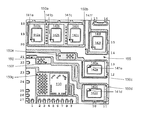
FIG. 1A shows a top view of a semiconductor package according to one embodiment of the present invention. In this example, the semiconductor package may comprise a 12 mm × 12 mm PQFN package (with a 12 mm × 12 mm footprint), which package includes 27 numbered external leads, namely
図1Aに示されるように、ドライバ集積回路(IC)、即ちドライバIC130、はパッケージ内に中心に置かれる。ドライバIC130はフルブリッジ構成の6個のパワーデバイスを駆動するのに好適な高電圧IC(HVIC)、例えばインターナショナル・レクティファイヤ・コーポレーション(登録商標)から入手し得る「第5世代」HVIC、を備えることができる。従って、ドライバIC130は縦導通型パワーデバイス140a、140b、140c、140d、140e及び140fのそれぞれのゲート電極141a、141b,141c,141d,141e及び141fに接続することができ、これらのパワーデバイスは、例えばファーストリバース・エピタキシャル・ダイオード・電界効果トランジスタ(FREDFET)のようなパワー金属−酸化物−半導体電界効果トランジスタ(パワーMOSFET)又は絶縁ゲートバイポーラトランジスタ(IGBT)を備えることができる。例えば、縦導通型パワーデバイス140a−140cはフルブリッジパワーデバイスのハイサイドFETを構成するMOSFETデバイスを備えることができ、縦導通型パワーデバイス140d−140fはフルブリッジパワーデバイスのローサイドFETを構成するMOSFETデバイスを備えることができる。
As shown in FIG. 1A, a driver integrated circuit (IC), or
明瞭のために、ドライバIC130と縦導通型パワーデバイス140a−140fとの間の接続を提供し得るワイヤボンドは図1Aから省略されている。更に、フルブリッジパワーデバイスを提供するパッケージが図に示されているが、代替実施例は特定の用途に必要とされる他のパッケージデバイス構成を提供することができる。
For clarity, wire bonds that may provide a connection between
リードフレーム160はオリン・ブラス(登録商標)から入手し得る銅(Cu)合金C194のような高い熱及び電気伝動率を有する材料で構成することができる。図1Cと関連して更に説示するように、最適な電気伝導率及び熱消散のためにリードフレーム160の底面の大きな部分を露出させることができる。リードフレーム160の上面はデバイスダイ及びワイヤへの付着強化用の材料で選択的にめっきすることもできる。例えば、めっき部150a、150b、150c,150d,150e,150f及び150gはリードフレーム160に選択的に被着された銀(Ag)めっきとすることができ、この銀めっきはQPLリミテッドなどの会社から入手できる。モールドコンパウンド165は日立ケミカル(登録商標)から入手し得る低い曲げ弾性率のコンパウンドを含むことができる。
The
図1Aに示されるように、縦導通型パワーデバイス140a−14cはパワーの上端縁の近くに位置する同じダイパッドを共用し、めっき部150aを経てリードフレーム160に結合される。従って、ハイサイドMOSFETのボトムドレイン電極はすべて同じダイパッドに一緒に接続される。他方、ローサイドMOSFETを備える縦導通型パワーデバイス140d−140fはそれぞれパワーの右端縁の近くに位置する個別のダイパッドに置かれる。縦導通型パワーデバイス140a−140cの底面をめっき部150aに取り付けるため、縦導通型パワーデバイス140a−140cの底面をめっき部150aに取り付けるため、縦導通型パワーデバイス140dの底面をめっき部150dに取り付けるため、縦導通型パワーデバイス140eの底面をめっき部150cに取り付けるため、縦導通型パワーデバイス140fの底面をめっき部150bに取り付けるため、及びドライバIC130をめっき部150gに取り付けるために、ヘンケルコーポレーションから入手し得る銀充填QMI529HTなどのはんだ又は導電性接着剤を使用することができる。
As shown in FIG. 1A, the vertical conduction
ドライバIC130及び縦導通型パワーデバイス140a−140fは電気伝導性にとって最適な態様でパッケージ内に定置される。図1Aのフルブリッジパッケージ回路を完成するために、ソース電極142aを縦導通型パワーデバイス140dのドレイン電極に接続し、ソース電極142bを縦導通型パワーデバイス140eのドレイン電極に接続し、ソース電極142cを縦導通型パワーデバイス140fのドレイン電極に接続し、ソース電極142d,142e及び142fを一緒に結合する必要がある。しかし、必要な接続を付与するようにワイヤを直接配線すること(ルーティング)はワイヤ交差及び潜在的なワイヤ短絡を生じ得る。更に、パッケージは高電力用を目標としているため、必要とされる長い配線長は電気的及び熱的性能に悪影響を与え得る。
Driver IC 130 and longitudinal
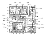
そこで、図1Bに戻り説明すると、図1Bは本発明の一実施例によるワイヤボンドを含む半導体パッケージの上面図を示す。図1Bに示されるように、ゲート配線用、電流検知用及び他のI/O機能用には、典型的なワイヤボンド170bで示されるような細いワイヤが使用される。これらのワイヤは、例えば直径1.3ミルのG1タイプの金(Au)ワイヤとすることができる。パワー接続用には典型的なワイヤボンド170aにより示されるような太いワイヤが使用される。これらのワイヤは直径2.0ミルの銅(Cu)ワイヤ、例えばクリッケ・アンド・ソッファ(登録商標)から入手し得るMaxsoft(登録商標)LDワイヤとすることができる。ワイヤボンド170aのような太いワイヤはボンド・ステッチ・オン・ボール(BSOB)ボンディングを用いてボンドすることができる。図1Bに示されるように、追加の電流処理能力を与えるために複数のワイヤボンド、例えば2つのワイヤボンドを並列に設置することができる。
Returning now to FIG. 1B, FIG. 1B shows a top view of a semiconductor package including wire bonds according to one embodiment of the present invention. As shown in FIG. 1B, thin wires as shown by
従って、図1Aから回路を完成し外部リード1−27に至る所要の接続は図1Bに示されるワイヤボンド及びリードフレーム160により与えられる。ゲート電極141a−141fの各々は金のワイヤボンドを用いてドライバIC130に直接接続される。縦導通型パワーデバイス140c及び140fはすでに近接近位置にあるため、1対の銅ワイヤを用いてソース電極142cとめっき部150bとの間に直接ワイヤボンドを行うことができる。
Thus, the required connections to complete the circuit from FIG. 1A to the external leads 1-27 are provided by the wire bonds and
しかし、もっと離れたデバイス間の接続には、リードフレーム160による配線を用いるのが有利である。リードフレーム160は銅合金のような高い伝導率の材料で構成されるため、リードフレーム160は直接ワイヤ配線に比較してはるかに効率的な導電通路を提供することができる。加えて、ワイヤ交差によるワイヤ短絡の危険のような問題も避けられる。
However, it is advantageous to use wiring by the
例えば、ソース電極142bを縦導通型パワーデバイス140eのドレイン電極に接続するために、1対の太い銅ワイヤがソース電極142bの上面とめっき部150eの上面との間にボンドされる。この接続は、以下に説明される図2に詳細に示され、この図は線102で切断されたスライスの断面図を示す。めっき部150eの下のリードフレーム160はそこからめっき部150cにつながっており、縦導通型パワーデバイス140eのドレイン電極への接続を完成する。同様に、ソース電極142aは1対の太いワイヤを経てめっき部150fにボンドされ、めっき部150fはそこからリードフレーム160を経て、縦導通型パワーデバイス140dのドレイン電極に接続されためっき部150dにつながっている。従って、パッケージを完成するために必要な電気的接続がリードフレームを配線装置として用いることによって与えられ、交差ワイヤボンドを有利に避けることができる。
For example, in order to connect the
図1Cに進むと、図1Cは本発明の一実施例による半導体パッケージの底面図を示す。図1Bに示すパッケージを反転すると、リードフレームの露出部分が見え、図1Cに示すレイアウトを見ることができる。例えば、リードフレーム部分160aは図1Bに示されるめっき部150aの外形に対応し、リードフレーム部分160bは図1Bに示されるめっき部150eの外形に対応する。従って、パッケージリードフレームの大部分が効率的な熱消散及び電気伝導率のために底面に露出される。露出表面部分も例えば錫(Sn)でめっきすることができる。それに応じて対応ランド部を備えるプリント回路盤(PCB)を設計することによって、効率的な設計のPQFNパッケージを有利に利用することができる。
Proceeding to FIG. 1C, FIG. 1C shows a bottom view of a semiconductor package according to one embodiment of the present invention. When the package shown in FIG. 1B is inverted, the exposed portion of the lead frame can be seen and the layout shown in FIG. 1C can be seen. For example, the lead frame portion 160a corresponds to the outer shape of the plated
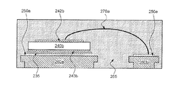
図2につき検討すると、図2は本発明の一実施例による半導体パッケージの一部分の断面図を示す。もっと正確に言うと、この断面図は図1Bの線102上の断面に相当する。図2において、リードフレーム260a及び260bは図1Cのリードフレーム160a及び160bに対応し、縦導通型パワーデバイス240bは図1Bの縦導通型パワーデバイス140bに対応し、ソース電極242bは図1Bのソース電極142bに対応し、めっき部250aは図1Bのめっき部150aに対応し、めっき部250eは図1Bのめっき部150eに対応し、モールドコンパウンド265は図1Bのモールドコンパウンド165に対応する。図2は必ずしも一定の寸法比で描かれていない点に注意されたい。
Considering FIG. 2, FIG. 2 shows a cross-sectional view of a portion of a semiconductor package according to one embodiment of the present invention. More precisely, this cross-sectional view corresponds to the cross-section on
図2に示されるように、縦導通型パワーデバイス240bのドレイン電極243bは導電性接着剤235及びめっき部250aを経てリードフレーム部分260aに結合される。先に述べたように、導電性接着剤235はQMI529HTなどの銀充填接着剤とすることができる。縦導通型パワーデバイス240bのソース電極242bはそこからワイヤボンド270a及びめっき部250eを経てリードフレーム部分260bに結合される。ワイヤボンド270aはBSOBボンドされる直径2.0ミルの銅(Cu)ワイヤとすることができる。先に述べたように、追加の電流処理能力のために複数のワイヤボンドを設けることもできるが、図1Bに示す1対のワイヤボンドは互いに平行配置されるために、図2には示されていない。デバイスダイが接着され、ワイヤボンドが形成された後に、パッケージはモールドコンパウンド265を用いてカプセル封止することができる。パッケージクラッキングに対抗する弾性を与えるために、モールドコンパウンド265により決まるパッケージの高さ(又は暑さ)は、例えば0.9mm以下の薄さに維持できる。
As shown in FIG. 2, the
従って、図2に示す断面は図1Bに示されるソース電極142bとめっき部150eを接続するワイヤボンド270aにより与えられる電気的接続を示している。図2のリードフレーム260bに対応する図1bのリードフレーム部分160は右方向に延びてめっき部150eにつながり、それによって縦導通型パワーデバイス140eのドレインへの接続が完成する。ソース電極142aを縦導通型パワーデバイス140dのドレインに接続するためにも同様の接続プロセスが適用される。
Therefore, the cross section shown in FIG. 2 shows the electrical connection provided by the
上に述べたように、電気的相互接続のためにリードフレームを用いるマルチチップモジュール(MCM)パワー・カッド・フラット・ノーリード(PQFN)半導体パッケージを説明した。本発明によれば、多数のパワーデバイスを備える複雑なパッケージでも効率的な電気的相互接続手段として低コストのリードフレームを利用することによって集積化できる。本発明の革新的なパッケージは、従来のパッケージ技術よりもコンパクトなフォームファクタ、向上した電気的及び熱的伝導性、向上した信頼性及び費用効率のよい製造を可能にする。 As described above, a multichip module (MCM) power quad flat no lead (PQFN) semiconductor package has been described that uses a lead frame for electrical interconnection. According to the present invention, even a complex package having a large number of power devices can be integrated by utilizing a low-cost lead frame as an efficient electrical interconnection means. The innovative package of the present invention allows for a more compact form factor, improved electrical and thermal conductivity, improved reliability and cost effective manufacturing than conventional packaging technology.
本発明の上述の説明から、本発明のコンセプトは本発明の範囲から離れることなく種々の技術を用いて実現できること明らかである。更に、本発明を特に所定の実施例について説明したが、本発明の精神及び範囲から離れることなく本発明の構造及び細部に変更を加えることができることは当業者に認識されよう。従って、開示の実施例はすべての点で例示であり、非限定的であるとみなされたい。本発明は開示の特定の実施例に限定されず、本発明の範囲から逸脱することなく多くの再構成、変更及び置換が可能であることを理解されたい。 From the above description of the invention it is manifest that the concepts of the invention can be implemented using various techniques without departing from the scope of the present invention. Further, while the invention has been described with particular reference to certain embodiments, those skilled in the art will recognize that changes can be made in the structure and details of the invention without departing from the spirit and scope of the invention. Accordingly, the disclosed embodiments are to be considered in all respects only as illustrative and not restrictive. It is to be understood that the invention is not limited to the specific embodiments disclosed, and that many reconfigurations, modifications and substitutions are possible without departing from the scope of the invention.
Claims (20)
前記リードフレームの第1のダイパッドに結合されたドライバ集積回路(IC)と、
前記リードフレームの第2のダイパッドに結合された第1群の縦導通型パワーデバイス及び前記リードフレームの対応するダイパッドに個別に結合された第2群の縦導通型パワーデバイスを含む複数の縦導通型パワーデバイスと、
前記ドライバIC、前記複数の縦導通型パワーデバイス及び前記リードフレームの複数の外部リードの間の電気的相互接続を与える複数のワイヤボンドとを備え、前記第1群の縦導通型パワーデバイスの一つの上面電極が前記第2群の縦導通型パワーデバイスの一つの底面電極に電気的に接続されている、
ことを特徴とするパワー・カッド・フラット・ノーリード(PQFN)半導体パッケージ。 A lead frame comprising a plurality of die pads;
A driver integrated circuit (IC) coupled to the first die pad of the lead frame;
A plurality of longitudinal conduction devices including a first group of longitudinal conduction power devices coupled to a second die pad of the lead frame and a second group of longitudinal conduction power devices individually coupled to corresponding die pads of the lead frame. Type power device,
A plurality of wire bonds that provide electrical interconnections between the driver ICs, the plurality of longitudinal conduction power devices and the plurality of external leads of the lead frame; Two top electrodes are electrically connected to one bottom electrode of the second group of longitudinal conduction power devices,
A power quad flat no lead (PQFN) semiconductor package.
前記リードフレームに結合されたドライバ集積回路(IC)と、
前記リードフレームに結合された複数の縦導通型パワーデバイスと、
前記ドライバIC、前記複数の縦導通型パワーデバイス及び前記リードフレームの複数の外部リードの間の電気的相互接続を与える複数のワイヤボンドとを備え、前記複数のワイヤボンドは、前記複数の縦導通型パワーデバイスの一つの上面電極から前記リードフレームの一部分への第1のワイヤボンドを含み、前記リードフレームの一部分は前記複数の縦導通型パワーデバイスの別の一つの底面電極に電気的に接続されている、
ことを特徴とするパワー・カッド・フラット・ノーリード(PQFN)半導体パッケージ。 A lead frame;
A driver integrated circuit (IC) coupled to the lead frame;
A plurality of longitudinal conduction type power devices coupled to the lead frame;
A plurality of wire bonds providing electrical interconnections between the driver ICs, the plurality of longitudinal conduction type power devices and a plurality of external leads of the lead frame, wherein the plurality of wire bonds are the plurality of longitudinal conductions. A first wire bond from one top electrode of the power device to a portion of the lead frame, wherein the lead frame portion is electrically connected to another bottom electrode of the plurality of longitudinal conduction power devices Being
A power quad flat no lead (PQFN) semiconductor package.
Applications Claiming Priority (4)
| Application Number | Priority Date | Filing Date | Title |
|---|---|---|---|
| US45952710P | 2010-12-13 | 2010-12-13 | |
| US61/459,527 | 2010-12-13 | ||
| US13/034,519 | 2011-02-24 | ||
| US13/034,519 US8587101B2 (en) | 2010-12-13 | 2011-02-24 | Multi-chip module (MCM) power quad flat no-lead (PQFN) semiconductor package utilizing a leadframe for electrical interconnections |
Related Child Applications (1)
| Application Number | Title | Priority Date | Filing Date |
|---|---|---|---|
| JP2013191041A Division JP2014060402A (en) | 2010-12-13 | 2013-09-13 | Multi-chip module (mcm) power quad flat no-lead (pqfn) semiconductor package utilizing leadframe for electrical interconnections |
Publications (1)
| Publication Number | Publication Date |
|---|---|
| JP2012129489A true JP2012129489A (en) | 2012-07-05 |
Family
ID=45715256
Family Applications (2)
| Application Number | Title | Priority Date | Filing Date |
|---|---|---|---|
| JP2011095296A Pending JP2012129489A (en) | 2010-12-13 | 2011-04-21 | Multi-chip module (mcm) power quad flat no-lead (pqfn) semiconductor package utilizing leadframe for electrical interconnections |
| JP2013191041A Pending JP2014060402A (en) | 2010-12-13 | 2013-09-13 | Multi-chip module (mcm) power quad flat no-lead (pqfn) semiconductor package utilizing leadframe for electrical interconnections |
Family Applications After (1)
| Application Number | Title | Priority Date | Filing Date |
|---|---|---|---|
| JP2013191041A Pending JP2014060402A (en) | 2010-12-13 | 2013-09-13 | Multi-chip module (mcm) power quad flat no-lead (pqfn) semiconductor package utilizing leadframe for electrical interconnections |
Country Status (5)
| Country | Link |
|---|---|
| US (4) | US8587101B2 (en) |
| EP (1) | EP2463904B1 (en) |
| JP (2) | JP2012129489A (en) |
| KR (3) | KR20120089542A (en) |
| CN (1) | CN102569241B (en) |
Cited By (20)
| Publication number | Priority date | Publication date | Assignee | Title |
|---|---|---|---|---|
| JP2014090006A (en) * | 2012-10-29 | 2014-05-15 | Mitsubishi Electric Corp | Power module |
| JP2014143271A (en) * | 2013-01-23 | 2014-08-07 | Fujitsu Semiconductor Ltd | Semiconductor device and manufacturing method of the same |
| JP2014175652A (en) * | 2013-03-07 | 2014-09-22 | Internatl Rectifier Corp | Open source power quad flat no-lead (pqfn) leadframe |
| JP2014175656A (en) * | 2013-03-12 | 2014-09-22 | Internatl Rectifier Corp | Control and driver circuits on power quad flat no-lead (pqfn) leadframe |
| JP2014175654A (en) * | 2013-03-07 | 2014-09-22 | Internatl Rectifier Corp | Power quad flat no-lead (pqfn) package having bootstrap diodes on common integrated circuit (ic) |
| JP2014179587A (en) * | 2013-03-07 | 2014-09-25 | Internatl Rectifier Corp | Power quad flat no-lead (pqfn) semiconductor package with leadframe islands for multi-phase power stage |
| JP2014179603A (en) * | 2013-03-12 | 2014-09-25 | Internatl Rectifier Corp | Power quad flat no-lead (pqfn) package having control and driver circuit |
| JP2014195045A (en) * | 2013-03-07 | 2014-10-09 | Internatl Rectifier Corp | Power quad flat no-lead package included in single shunt inverter circuit |
| JP2015002185A (en) * | 2013-06-13 | 2015-01-05 | 三菱電機株式会社 | Power semiconductor device |
| JP2015106685A (en) * | 2013-12-02 | 2015-06-08 | 三菱電機株式会社 | Power module and method of manufacturing the same |
| US9324646B2 (en) | 2010-12-13 | 2016-04-26 | Infineon Technologies America Corp. | Open source power quad flat no-lead (PQFN) package |
| US9324638B2 (en) | 2010-12-13 | 2016-04-26 | Infineon Technologies Americas Corp. | Compact wirebonded power quad flat no-lead (PQFN) package |
| US9362215B2 (en) | 2010-12-13 | 2016-06-07 | Infineon Technologies Americas Corp. | Power quad flat no-lead (PQFN) semiconductor package with leadframe islands for multi-phase power inverter |
| US9443795B2 (en) | 2010-12-13 | 2016-09-13 | Infineon Technologies Americas Corp. | Power quad flat no-lead (PQFN) package having bootstrap diodes on a common integrated circuit (IC) |
| US9449957B2 (en) | 2010-12-13 | 2016-09-20 | Infineon Technologies Americas Corp. | Control and driver circuits on a power quad flat no-lead (PQFN) leadframe |
| US9524928B2 (en) | 2010-12-13 | 2016-12-20 | Infineon Technologies Americas Corp. | Power quad flat no-lead (PQFN) package having control and driver circuits |
| US9620954B2 (en) | 2010-12-13 | 2017-04-11 | Infineon Technologies Americas Corp. | Semiconductor package having an over-temperature protection circuit utilizing multiple temperature threshold values |
| US9659845B2 (en) | 2010-12-13 | 2017-05-23 | Infineon Technologies Americas Corp. | Power quad flat no-lead (PQFN) package in a single shunt inverter circuit |
| US9711437B2 (en) | 2010-12-13 | 2017-07-18 | Infineon Technologies Americas Corp. | Semiconductor package having multi-phase power inverter with internal temperature sensor |
| WO2019203139A1 (en) * | 2018-04-19 | 2019-10-24 | ローム株式会社 | Semiconductor device |
Families Citing this family (26)
| Publication number | Priority date | Publication date | Assignee | Title |
|---|---|---|---|---|
| US9355995B2 (en) | 2010-12-13 | 2016-05-31 | Infineon Technologies Americas Corp. | Semiconductor packages utilizing leadframe panels with grooves in connecting bars |
| US9717146B2 (en) | 2012-05-22 | 2017-07-25 | Intersil Americas LLC | Circuit module such as a high-density lead frame array (HDA) power module, and method of making same |
| US20140070329A1 (en) | 2012-09-07 | 2014-03-13 | Fairchild Semiconductor Corporation | Wireless module with active and passive components |
| KR102071078B1 (en) * | 2012-12-06 | 2020-01-30 | 매그나칩 반도체 유한회사 | Multi chip package |
| US9202811B2 (en) * | 2012-12-18 | 2015-12-01 | Infineon Technologies Americas Corp. | Cascode circuit integration of group III-N and group IV devices |
| US9379048B2 (en) * | 2013-02-28 | 2016-06-28 | Semiconductor Components Industries, Llc | Dual-flag stacked die package |
| EP2779227A3 (en) * | 2013-03-13 | 2017-11-22 | International Rectifier Corporation | Semiconductor package having multi-phase power inverter with internal temperature sensor |
| US9147664B2 (en) * | 2013-10-11 | 2015-09-29 | Mediatek Inc. | Semiconductor package |
| CN104681526B (en) * | 2013-11-28 | 2017-07-04 | 无锡华润华晶微电子有限公司 | A kind of encapsulating structure for Dimmable LED constant-current drive circuit |
| US9536800B2 (en) | 2013-12-07 | 2017-01-03 | Fairchild Semiconductor Corporation | Packaged semiconductor devices and methods of manufacturing |
| WO2015134025A1 (en) | 2014-03-06 | 2015-09-11 | Otis Elevator Company | Fiber reinforced elevator belt and method of manufacture |
| KR101555301B1 (en) * | 2014-05-13 | 2015-09-23 | 페어차일드코리아반도체 주식회사 | Semiconductor package |
| EP3257336A4 (en) * | 2014-12-10 | 2018-10-10 | Texas Instruments Incorporated | Power field-effect transistor (fet), pre-driver, controller, and sense resistor integration |
| CN105118818B (en) | 2015-07-20 | 2018-08-21 | 东南大学 | A kind of power module of square flat pin-free packaging structure |
| TWI657554B (en) * | 2015-09-30 | 2019-04-21 | 台達電子工業股份有限公司 | Package structure |
| WO2018109069A1 (en) * | 2016-12-16 | 2018-06-21 | Abb Schweiz Ag | Power semiconductor module with low gate path inductance |
| US10396774B2 (en) | 2017-09-14 | 2019-08-27 | Hestia Power Inc. | Intelligent power module operable to be driven by negative gate voltage |
| TWI640151B (en) * | 2017-09-20 | 2018-11-01 | 瀚薪科技股份有限公司 | Negative voltage gate driven smart power module |
| KR102475429B1 (en) * | 2017-11-24 | 2022-12-08 | 주식회사 케이티 | Method for allocating resource based on data traffic analysis and apparatus thereof |
| US10714411B2 (en) | 2018-03-15 | 2020-07-14 | Globalfoundries Inc. | Interconnected integrated circuit (IC) chip structure and packaging and method of forming same |
| US10742217B2 (en) | 2018-04-12 | 2020-08-11 | Apple Inc. | Systems and methods for implementing a scalable system |
| EP3703123A1 (en) | 2019-02-27 | 2020-09-02 | Infineon Technologies Austria AG | Semiconductor component and semiconductor package |
| TWI693682B (en) * | 2019-08-28 | 2020-05-11 | 財團法人工業技術研究院 | Electronic device package structure |
| US11145609B2 (en) | 2019-12-05 | 2021-10-12 | Nxp Usa, Inc. | Doherty amplifier with surface-mount packaged carrier and peaking amplifiers |
| EP3975225A1 (en) | 2020-09-24 | 2022-03-30 | Infineon Technologies Austria AG | Semiconductor module |
| EP3982404A1 (en) | 2020-10-07 | 2022-04-13 | Infineon Technologies Austria AG | Semiconductor module |
Citations (10)
| Publication number | Priority date | Publication date | Assignee | Title |
|---|---|---|---|---|
| JPH09102580A (en) * | 1995-08-02 | 1997-04-15 | Matsushita Electron Corp | Resin-sealed semiconductor device and fabrication thereof |
| WO1998024128A1 (en) * | 1996-11-28 | 1998-06-04 | Mitsubishi Denki Kabushiki Kaisha | Semiconductor device |
| JP2004342735A (en) * | 2003-05-14 | 2004-12-02 | Renesas Technology Corp | Semiconductor device and power supply system |
| JP2005086200A (en) * | 2003-09-04 | 2005-03-31 | Samsung Electronics Co Ltd | Wire bonding method, semiconductor chip and semiconductor package |
| JP2005217072A (en) * | 2004-01-28 | 2005-08-11 | Renesas Technology Corp | Semiconductor device |
| JP2005294464A (en) * | 2004-03-31 | 2005-10-20 | Renesas Technology Corp | Semiconductor device |
| JP2007227416A (en) * | 2006-02-21 | 2007-09-06 | Renesas Technology Corp | Semiconductor device and process for manufacturing the same |
| JP2007266218A (en) * | 2006-03-28 | 2007-10-11 | Renesas Technology Corp | Semiconductor device, and its manufacturing method |
| JP2008034567A (en) * | 2006-07-27 | 2008-02-14 | Fujitsu Ltd | Semiconductor device and manufacturing method therefor |
| JP2010067755A (en) * | 2008-09-10 | 2010-03-25 | Renesas Technology Corp | Semiconductor device |
Family Cites Families (67)
| Publication number | Priority date | Publication date | Assignee | Title |
|---|---|---|---|---|
| JP3384399B2 (en) | 1995-06-28 | 2003-03-10 | 富士電機株式会社 | High withstand voltage level shift circuit for high withstand voltage IC |
| JP3394377B2 (en) | 1996-01-09 | 2003-04-07 | 三菱電機株式会社 | Semiconductor device and semiconductor module |
| JP3431467B2 (en) | 1997-09-17 | 2003-07-28 | 株式会社東芝 | High voltage semiconductor device |
| JP3674333B2 (en) | 1998-09-11 | 2005-07-20 | 株式会社日立製作所 | Power semiconductor module and electric motor drive system using the same |
| US6249024B1 (en) * | 1998-12-09 | 2001-06-19 | International Rectifier Corp. | Power module with repositioned positive and reduced inductance and capacitance |
| US6137165A (en) | 1999-06-25 | 2000-10-24 | International Rectifier Corp. | Hybrid package including a power MOSFET die and a control and protection circuit die with a smaller sense MOSFET |
| JP3813775B2 (en) | 1999-11-05 | 2006-08-23 | ローム株式会社 | Multi-chip module |
| JP2001135765A (en) | 1999-11-05 | 2001-05-18 | Hitachi Cable Ltd | Method and device for manufacturing composite lead frame |
| US6465875B2 (en) | 2000-03-27 | 2002-10-15 | International Rectifier Corporation | Semiconductor device package with plural pad lead frame |
| JP2002217416A (en) | 2001-01-16 | 2002-08-02 | Hitachi Ltd | Semiconductor device |
| JP4286465B2 (en) | 2001-02-09 | 2009-07-01 | 三菱電機株式会社 | Semiconductor device and manufacturing method thereof |
| DE10107386C1 (en) | 2001-02-16 | 2002-08-22 | Infineon Technologies Ag | Circuit arrangement with temperature protection and process |
| JP4450530B2 (en) | 2001-07-03 | 2010-04-14 | 三菱電機株式会社 | Inverter module |
| US20030107120A1 (en) * | 2001-12-11 | 2003-06-12 | International Rectifier Corporation | Intelligent motor drive module with injection molded package |
| KR100833934B1 (en) | 2002-01-24 | 2008-05-30 | 삼성테크윈 주식회사 | Multi-layer plating lead frame and method of manufacturing the same |
| JP4127014B2 (en) | 2002-10-23 | 2008-07-30 | 株式会社豊田自動織機 | Current detection device and inverter device with current detection function |
| US20040227476A1 (en) | 2002-12-19 | 2004-11-18 | International Rectifier Corp. | Flexible inverter power module for motor drives |
| US7215012B2 (en) * | 2003-01-03 | 2007-05-08 | Gem Services, Inc. | Space-efficient package for laterally conducting device |
| JP4044861B2 (en) | 2003-04-03 | 2008-02-06 | 三菱電機株式会社 | Power conversion device and power conversion system device including the power conversion device |
| JP4004460B2 (en) | 2003-12-16 | 2007-11-07 | 三菱電機株式会社 | Semiconductor device |
| JP4565879B2 (en) | 2004-04-19 | 2010-10-20 | ルネサスエレクトロニクス株式会社 | Semiconductor device |
| US7609024B2 (en) | 2004-05-27 | 2009-10-27 | Siemens Energy & Automation, Inc. | Auxiliary bus method |
| US7298027B2 (en) | 2004-09-02 | 2007-11-20 | International Rectifier Corporation | SMT three phase inverter package and lead frame |
| JP4426955B2 (en) * | 2004-11-30 | 2010-03-03 | 株式会社ルネサステクノロジ | Semiconductor device |
| JP4624170B2 (en) * | 2005-04-25 | 2011-02-02 | ルネサスエレクトロニクス株式会社 | Manufacturing method of semiconductor device |
| KR101321361B1 (en) | 2005-09-05 | 2013-10-22 | 페어차일드코리아반도체 주식회사 | Inverter module for motor drive and motor driving apparatus having the same and inverter integrated circuit package |
| JP2007082036A (en) | 2005-09-16 | 2007-03-29 | Rohm Co Ltd | Semiconductor integrated circuit device, power supply apparatus, and electric apparatus |
| JP2007082365A (en) | 2005-09-16 | 2007-03-29 | Rohm Co Ltd | Temperature protection circuit, power supply device, and electronic apparatus |
| TWI288801B (en) | 2005-11-23 | 2007-10-21 | Delta Electronics Inc | Fan system and temperature-sensing protecting device thereof |
| US7943431B2 (en) | 2005-12-02 | 2011-05-17 | Unisem (Mauritius) Holdings Limited | Leadless semiconductor package and method of manufacture |
| JP4875380B2 (en) | 2006-02-24 | 2012-02-15 | ルネサスエレクトロニクス株式会社 | Semiconductor device |
| DE102006012781B4 (en) | 2006-03-17 | 2016-06-16 | Infineon Technologies Ag | Multichip module with improved system carrier and method for its production |
| KR101340966B1 (en) | 2006-05-24 | 2013-12-13 | 페어차일드코리아반도체 주식회사 | 3 phase inverter module, motor driving apparatus using the same, and inverter integrated circuit package |
| US7830104B2 (en) | 2006-09-19 | 2010-11-09 | Seiko Epson Corporation | Brushless motor |
| JP2008160933A (en) | 2006-12-21 | 2008-07-10 | Sharp Corp | Chopper regulator circuit |
| DE102007013186B4 (en) | 2007-03-15 | 2020-07-02 | Infineon Technologies Ag | Semiconductor module with semiconductor chips and method for producing the same |
| US8427235B2 (en) * | 2007-04-13 | 2013-04-23 | Advanced Analogic Technologies, Inc. | Power-MOSFETs with improved efficiency for multi-channel class-D audio amplifiers and packaging thereof |
| JP4973359B2 (en) | 2007-07-23 | 2012-07-11 | 富士電機株式会社 | Semiconductor device |
| US7732917B2 (en) | 2007-10-02 | 2010-06-08 | Rohm Co., Ltd. | Power module |
| US20090189261A1 (en) | 2008-01-25 | 2009-07-30 | Lay Yeap Lim | Ultra-Thin Semiconductor Package |
| TWI347737B (en) | 2008-02-27 | 2011-08-21 | Prolific Technology Inc | Method and pwm system of adjusting the width of pulses through collecting information of a three-phase current |
| US20090261462A1 (en) * | 2008-04-16 | 2009-10-22 | Jocel Gomez | Semiconductor package with stacked die assembly |
| JP4620151B2 (en) | 2008-12-12 | 2011-01-26 | 東光株式会社 | Non-contact power transmission circuit |
| JP5284077B2 (en) | 2008-12-26 | 2013-09-11 | 株式会社日立製作所 | Semiconductor device and power conversion device using the same |
| US20100301464A1 (en) | 2009-05-26 | 2010-12-02 | Mohamad Ashraf Bin Mohd Arshad | Asterisk pad |
| JP2011029262A (en) | 2009-07-22 | 2011-02-10 | Daikin Industries Ltd | Power converter |
| US8362598B2 (en) | 2009-08-26 | 2013-01-29 | Amkor Technology Inc | Semiconductor device with electromagnetic interference shielding |
| US8456794B2 (en) | 2009-11-12 | 2013-06-04 | Infineon Technologies Ag | Clock-pulsed safety switch |
| CN101814480B (en) | 2010-04-16 | 2011-08-31 | 杭州矽力杰半导体技术有限公司 | Chip package structure and packaging method thereof |
| US20120126378A1 (en) | 2010-11-24 | 2012-05-24 | Unisem (Mauritius ) Holdings Limited | Semiconductor device package with electromagnetic shielding |
| US9324646B2 (en) | 2010-12-13 | 2016-04-26 | Infineon Technologies America Corp. | Open source power quad flat no-lead (PQFN) package |
| US8587101B2 (en) | 2010-12-13 | 2013-11-19 | International Rectifier Corporation | Multi-chip module (MCM) power quad flat no-lead (PQFN) semiconductor package utilizing a leadframe for electrical interconnections |
| US9355995B2 (en) | 2010-12-13 | 2016-05-31 | Infineon Technologies Americas Corp. | Semiconductor packages utilizing leadframe panels with grooves in connecting bars |
| US9449957B2 (en) | 2010-12-13 | 2016-09-20 | Infineon Technologies Americas Corp. | Control and driver circuits on a power quad flat no-lead (PQFN) leadframe |
| US9711437B2 (en) | 2010-12-13 | 2017-07-18 | Infineon Technologies Americas Corp. | Semiconductor package having multi-phase power inverter with internal temperature sensor |
| US9524928B2 (en) | 2010-12-13 | 2016-12-20 | Infineon Technologies Americas Corp. | Power quad flat no-lead (PQFN) package having control and driver circuits |
| US9362215B2 (en) | 2010-12-13 | 2016-06-07 | Infineon Technologies Americas Corp. | Power quad flat no-lead (PQFN) semiconductor package with leadframe islands for multi-phase power inverter |
| US9659845B2 (en) | 2010-12-13 | 2017-05-23 | Infineon Technologies Americas Corp. | Power quad flat no-lead (PQFN) package in a single shunt inverter circuit |
| US9443795B2 (en) | 2010-12-13 | 2016-09-13 | Infineon Technologies Americas Corp. | Power quad flat no-lead (PQFN) package having bootstrap diodes on a common integrated circuit (IC) |
| US9620954B2 (en) | 2010-12-13 | 2017-04-11 | Infineon Technologies Americas Corp. | Semiconductor package having an over-temperature protection circuit utilizing multiple temperature threshold values |
| US8803499B2 (en) | 2011-02-23 | 2014-08-12 | International Recifier Corporation | Power supply circuitry and adaptive transient control |
| JP2012175070A (en) | 2011-02-24 | 2012-09-10 | Panasonic Corp | Semiconductor package |
| CN102184917B (en) | 2011-03-25 | 2013-04-03 | 锐迪科创微电子(北京)有限公司 | Global system for mobile communications (GSM) radio-frequency emission front-end module adopting Quad Flat No-lead package |
| JP5757145B2 (en) | 2011-04-19 | 2015-07-29 | 富士電機株式会社 | Semiconductor device |
| JP5805513B2 (en) | 2011-12-14 | 2015-11-04 | 三菱電機株式会社 | Power semiconductor device |
| JP2014099547A (en) | 2012-11-15 | 2014-05-29 | Mitsubishi Electric Corp | Power semiconductor module and method of manufacturing the same |
| US20140272094A1 (en) | 2013-03-12 | 2014-09-18 | Advanced Food Systems, Inc. | Textured vegetable protein as a meat substitute and method and composition for making same |
-
2011
- 2011-02-24 US US13/034,519 patent/US8587101B2/en active Active
- 2011-04-21 JP JP2011095296A patent/JP2012129489A/en active Pending
- 2011-04-21 KR KR20110037503A patent/KR20120089542A/en not_active Application Discontinuation
- 2011-05-05 EP EP11165008.1A patent/EP2463904B1/en active Active
- 2011-05-11 KR KR1020110044073A patent/KR101281660B1/en active IP Right Grant
- 2011-05-13 CN CN201110126379.7A patent/CN102569241B/en active Active
-
2012
- 2012-10-26 US US13/662,244 patent/US9324638B2/en active Active
-
2013
- 2013-06-04 KR KR1020130064141A patent/KR101372900B1/en active IP Right Grant
- 2013-09-13 JP JP2013191041A patent/JP2014060402A/en active Pending
- 2013-11-11 US US14/076,467 patent/US9024420B2/en active Active
-
2015
- 2015-04-30 US US14/701,292 patent/US9530724B2/en active Active
Patent Citations (10)
| Publication number | Priority date | Publication date | Assignee | Title |
|---|---|---|---|---|
| JPH09102580A (en) * | 1995-08-02 | 1997-04-15 | Matsushita Electron Corp | Resin-sealed semiconductor device and fabrication thereof |
| WO1998024128A1 (en) * | 1996-11-28 | 1998-06-04 | Mitsubishi Denki Kabushiki Kaisha | Semiconductor device |
| JP2004342735A (en) * | 2003-05-14 | 2004-12-02 | Renesas Technology Corp | Semiconductor device and power supply system |
| JP2005086200A (en) * | 2003-09-04 | 2005-03-31 | Samsung Electronics Co Ltd | Wire bonding method, semiconductor chip and semiconductor package |
| JP2005217072A (en) * | 2004-01-28 | 2005-08-11 | Renesas Technology Corp | Semiconductor device |
| JP2005294464A (en) * | 2004-03-31 | 2005-10-20 | Renesas Technology Corp | Semiconductor device |
| JP2007227416A (en) * | 2006-02-21 | 2007-09-06 | Renesas Technology Corp | Semiconductor device and process for manufacturing the same |
| JP2007266218A (en) * | 2006-03-28 | 2007-10-11 | Renesas Technology Corp | Semiconductor device, and its manufacturing method |
| JP2008034567A (en) * | 2006-07-27 | 2008-02-14 | Fujitsu Ltd | Semiconductor device and manufacturing method therefor |
| JP2010067755A (en) * | 2008-09-10 | 2010-03-25 | Renesas Technology Corp | Semiconductor device |
Cited By (28)
| Publication number | Priority date | Publication date | Assignee | Title |
|---|---|---|---|---|
| US9899302B2 (en) | 2010-12-13 | 2018-02-20 | Infineon Technologies Americas Corp. | Semiconductor package having multi-phase power inverter with internal temperature sensor |
| US9324646B2 (en) | 2010-12-13 | 2016-04-26 | Infineon Technologies America Corp. | Open source power quad flat no-lead (PQFN) package |
| US9362215B2 (en) | 2010-12-13 | 2016-06-07 | Infineon Technologies Americas Corp. | Power quad flat no-lead (PQFN) semiconductor package with leadframe islands for multi-phase power inverter |
| US9443795B2 (en) | 2010-12-13 | 2016-09-13 | Infineon Technologies Americas Corp. | Power quad flat no-lead (PQFN) package having bootstrap diodes on a common integrated circuit (IC) |
| US10438876B2 (en) | 2010-12-13 | 2019-10-08 | Infineon Technologies Americas Corp. | Power quad flat no-lead (PQFN) package in a single shunt inverter circuit |
| US9524928B2 (en) | 2010-12-13 | 2016-12-20 | Infineon Technologies Americas Corp. | Power quad flat no-lead (PQFN) package having control and driver circuits |
| US9711437B2 (en) | 2010-12-13 | 2017-07-18 | Infineon Technologies Americas Corp. | Semiconductor package having multi-phase power inverter with internal temperature sensor |
| US9530724B2 (en) | 2010-12-13 | 2016-12-27 | Infineon Technologies Americas Corp. | Compact power quad flat no-lead (PQFN) package |
| US9449957B2 (en) | 2010-12-13 | 2016-09-20 | Infineon Technologies Americas Corp. | Control and driver circuits on a power quad flat no-lead (PQFN) leadframe |
| US9620954B2 (en) | 2010-12-13 | 2017-04-11 | Infineon Technologies Americas Corp. | Semiconductor package having an over-temperature protection circuit utilizing multiple temperature threshold values |
| US9659845B2 (en) | 2010-12-13 | 2017-05-23 | Infineon Technologies Americas Corp. | Power quad flat no-lead (PQFN) package in a single shunt inverter circuit |
| US9324638B2 (en) | 2010-12-13 | 2016-04-26 | Infineon Technologies Americas Corp. | Compact wirebonded power quad flat no-lead (PQFN) package |
| JP2014090006A (en) * | 2012-10-29 | 2014-05-15 | Mitsubishi Electric Corp | Power module |
| JP2014143271A (en) * | 2013-01-23 | 2014-08-07 | Fujitsu Semiconductor Ltd | Semiconductor device and manufacturing method of the same |
| JP2014195045A (en) * | 2013-03-07 | 2014-10-09 | Internatl Rectifier Corp | Power quad flat no-lead package included in single shunt inverter circuit |
| JP2014175654A (en) * | 2013-03-07 | 2014-09-22 | Internatl Rectifier Corp | Power quad flat no-lead (pqfn) package having bootstrap diodes on common integrated circuit (ic) |
| JP2014175652A (en) * | 2013-03-07 | 2014-09-22 | Internatl Rectifier Corp | Open source power quad flat no-lead (pqfn) leadframe |
| JP2014179587A (en) * | 2013-03-07 | 2014-09-25 | Internatl Rectifier Corp | Power quad flat no-lead (pqfn) semiconductor package with leadframe islands for multi-phase power stage |
| JP2014179603A (en) * | 2013-03-12 | 2014-09-25 | Internatl Rectifier Corp | Power quad flat no-lead (pqfn) package having control and driver circuit |
| JP2014175656A (en) * | 2013-03-12 | 2014-09-22 | Internatl Rectifier Corp | Control and driver circuits on power quad flat no-lead (pqfn) leadframe |
| JP2015002185A (en) * | 2013-06-13 | 2015-01-05 | 三菱電機株式会社 | Power semiconductor device |
| US10229867B2 (en) | 2013-06-13 | 2019-03-12 | Mitsubishi Electric Corporation | Power semiconductor device |
| US9716058B2 (en) | 2013-12-02 | 2017-07-25 | Mitsubishi Electric Corporation | Power module and control integrated circuit |
| JP2015106685A (en) * | 2013-12-02 | 2015-06-08 | 三菱電機株式会社 | Power module and method of manufacturing the same |
| US10332869B2 (en) | 2013-12-02 | 2019-06-25 | Mitsubishi Electric Corporation | Method for manufacturing power module |
| WO2019203139A1 (en) * | 2018-04-19 | 2019-10-24 | ローム株式会社 | Semiconductor device |
| JPWO2019203139A1 (en) * | 2018-04-19 | 2021-03-18 | ローム株式会社 | Semiconductor device |
| US11227822B2 (en) | 2018-04-19 | 2022-01-18 | Rohm Co., Ltd. | Semiconductor device |
Also Published As
| Publication number | Publication date |
|---|---|
| US20140061885A1 (en) | 2014-03-06 |
| US20130105958A1 (en) | 2013-05-02 |
| US20150235932A1 (en) | 2015-08-20 |
| CN102569241B (en) | 2015-03-04 |
| EP2463904B1 (en) | 2019-02-27 |
| JP2014060402A (en) | 2014-04-03 |
| KR20120089542A (en) | 2012-08-13 |
| CN102569241A (en) | 2012-07-11 |
| US9324638B2 (en) | 2016-04-26 |
| US9530724B2 (en) | 2016-12-27 |
| US20120146205A1 (en) | 2012-06-14 |
| US9024420B2 (en) | 2015-05-05 |
| KR101372900B1 (en) | 2014-03-10 |
| EP2463904A3 (en) | 2013-09-04 |
| KR101281660B1 (en) | 2013-07-08 |
| KR20120089543A (en) | 2012-08-13 |
| EP2463904A2 (en) | 2012-06-13 |
| US8587101B2 (en) | 2013-11-19 |
| KR20130071456A (en) | 2013-06-28 |
Similar Documents
| Publication | Publication Date | Title |
|---|---|---|
| KR101372900B1 (en) | Multi-chip module (mcm) power quad flat no-lead (pqfn) semiconductor package utilizing a leadframe for electrical interconnections | |
| US9589868B2 (en) | Packaging solutions for devices and systems comprising lateral GaN power transistors | |
| US9824949B2 (en) | Packaging solutions for devices and systems comprising lateral GaN power transistors | |
| US7227198B2 (en) | Half-bridge package | |
| US8828801B2 (en) | Leadless array plastic package with various IC packaging configurations | |
| JP2005217072A (en) | Semiconductor device | |
| US9468087B1 (en) | Power module with improved cooling and method for making | |
| US20220223568A1 (en) | Semiconductor device | |
| JP4250191B2 (en) | Semiconductor device for DC / DC converter | |
| US9355995B2 (en) | Semiconductor packages utilizing leadframe panels with grooves in connecting bars | |
| US10879155B2 (en) | Electronic device with double-sided cooling | |
| JP2023021365A (en) | Semiconductor device and power conversion device | |
| JP4705945B2 (en) | Semiconductor device | |
| US10892210B2 (en) | Package structures | |
| TW202015187A (en) | Molded intelligent power module for motors | |
| JP4800290B2 (en) | Semiconductor device | |
| JP2005051038A (en) | Semiconductor device and its manufacturing method | |
| JP2008091945A (en) | Semiconductor device |
Legal Events
| Date | Code | Title | Description |
|---|---|---|---|
| A977 | Report on retrieval |
Free format text: JAPANESE INTERMEDIATE CODE: A971007 Effective date: 20121116 |
|
| A131 | Notification of reasons for refusal |
Free format text: JAPANESE INTERMEDIATE CODE: A131 Effective date: 20121120 |
|
| A601 | Written request for extension of time |
Free format text: JAPANESE INTERMEDIATE CODE: A601 Effective date: 20121218 |
|
| A602 | Written permission of extension of time |
Free format text: JAPANESE INTERMEDIATE CODE: A602 Effective date: 20121221 |
|
| A601 | Written request for extension of time |
Free format text: JAPANESE INTERMEDIATE CODE: A601 Effective date: 20130314 |
|
| A602 | Written permission of extension of time |
Free format text: JAPANESE INTERMEDIATE CODE: A602 Effective date: 20130319 |
|
| A521 | Request for written amendment filed |
Free format text: JAPANESE INTERMEDIATE CODE: A523 Effective date: 20130419 |
|
| A02 | Decision of refusal |
Free format text: JAPANESE INTERMEDIATE CODE: A02 Effective date: 20130521 |
|
| A521 | Request for written amendment filed |
Free format text: JAPANESE INTERMEDIATE CODE: A523 Effective date: 20130913 |
|
| A911 | Transfer to examiner for re-examination before appeal (zenchi) |
Free format text: JAPANESE INTERMEDIATE CODE: A911 Effective date: 20130925 |
|
| A912 | Re-examination (zenchi) completed and case transferred to appeal board |
Free format text: JAPANESE INTERMEDIATE CODE: A912 Effective date: 20131129 |
|
| A601 | Written request for extension of time |
Free format text: JAPANESE INTERMEDIATE CODE: A601 Effective date: 20140422 |
|
| A602 | Written permission of extension of time |
Free format text: JAPANESE INTERMEDIATE CODE: A602 Effective date: 20140425 |
|
| A601 | Written request for extension of time |
Free format text: JAPANESE INTERMEDIATE CODE: A601 Effective date: 20140522 |
|
| A602 | Written permission of extension of time |
Free format text: JAPANESE INTERMEDIATE CODE: A602 Effective date: 20140527 |
|
| A601 | Written request for extension of time |
Free format text: JAPANESE INTERMEDIATE CODE: A601 Effective date: 20141030 |
|
| A602 | Written permission of extension of time |
Free format text: JAPANESE INTERMEDIATE CODE: A602 Effective date: 20141105 |
|
| A601 | Written request for extension of time |
Free format text: JAPANESE INTERMEDIATE CODE: A601 Effective date: 20141218 |
|
| A602 | Written permission of extension of time |
Free format text: JAPANESE INTERMEDIATE CODE: A602 Effective date: 20141224 |
|
| A601 | Written request for extension of time |
Free format text: JAPANESE INTERMEDIATE CODE: A601 Effective date: 20150123 |
|
| A521 | Request for written amendment filed |
Free format text: JAPANESE INTERMEDIATE CODE: A523 Effective date: 20150225 |