JP2012123889A - 半導体装置 - Google Patents
半導体装置 Download PDFInfo
- Publication number
- JP2012123889A JP2012123889A JP2011168083A JP2011168083A JP2012123889A JP 2012123889 A JP2012123889 A JP 2012123889A JP 2011168083 A JP2011168083 A JP 2011168083A JP 2011168083 A JP2011168083 A JP 2011168083A JP 2012123889 A JP2012123889 A JP 2012123889A
- Authority
- JP
- Japan
- Prior art keywords
- refresh
- signal
- control circuit
- semiconductor device
- reset
- Prior art date
- Legal status (The legal status is an assumption and is not a legal conclusion. Google has not performed a legal analysis and makes no representation as to the accuracy of the status listed.)
- Abandoned
Links
- 239000004065 semiconductor Substances 0.000 title claims abstract description 37
- 230000004044 response Effects 0.000 claims abstract description 11
- 230000004913 activation Effects 0.000 claims abstract description 10
- 230000007704 transition Effects 0.000 claims description 14
- 230000005540 biological transmission Effects 0.000 claims 2
- 230000001960 triggered effect Effects 0.000 claims 2
- 230000002779 inactivation Effects 0.000 claims 1
- 230000009849 deactivation Effects 0.000 abstract description 2
- 108090001145 Nuclear Receptor Coactivator 3 Proteins 0.000 description 18
- 102100022883 Nuclear receptor coactivator 3 Human genes 0.000 description 18
- 238000010586 diagram Methods 0.000 description 12
- 238000000034 method Methods 0.000 description 10
- 230000008569 process Effects 0.000 description 10
- 101100194362 Schizosaccharomyces pombe (strain 972 / ATCC 24843) res1 gene Proteins 0.000 description 8
- 238000007562 laser obscuration time method Methods 0.000 description 3
- 230000001934 delay Effects 0.000 description 2
- 230000003111 delayed effect Effects 0.000 description 2
- 230000004048 modification Effects 0.000 description 2
- 238000012986 modification Methods 0.000 description 2
- 230000000630 rising effect Effects 0.000 description 2
- 101100194363 Schizosaccharomyces pombe (strain 972 / ATCC 24843) res2 gene Proteins 0.000 description 1
- 230000003213 activating effect Effects 0.000 description 1
- 230000008901 benefit Effects 0.000 description 1
- 230000000295 complement effect Effects 0.000 description 1
- 230000006870 function Effects 0.000 description 1
- 230000001737 promoting effect Effects 0.000 description 1
- 230000001360 synchronised effect Effects 0.000 description 1
Images


Classifications
-
- G—PHYSICS
- G11—INFORMATION STORAGE
- G11C—STATIC STORES
- G11C11/00—Digital stores characterised by the use of particular electric or magnetic storage elements; Storage elements therefor
- G11C11/21—Digital stores characterised by the use of particular electric or magnetic storage elements; Storage elements therefor using electric elements
- G11C11/34—Digital stores characterised by the use of particular electric or magnetic storage elements; Storage elements therefor using electric elements using semiconductor devices
- G11C11/40—Digital stores characterised by the use of particular electric or magnetic storage elements; Storage elements therefor using electric elements using semiconductor devices using transistors
- G11C11/401—Digital stores characterised by the use of particular electric or magnetic storage elements; Storage elements therefor using electric elements using semiconductor devices using transistors forming cells needing refreshing or charge regeneration, i.e. dynamic cells
- G11C11/406—Management or control of the refreshing or charge-regeneration cycles
- G11C11/40615—Internal triggering or timing of refresh, e.g. hidden refresh, self refresh, pseudo-SRAMs
-
- G—PHYSICS
- G11—INFORMATION STORAGE
- G11C—STATIC STORES
- G11C11/00—Digital stores characterised by the use of particular electric or magnetic storage elements; Storage elements therefor
- G11C11/21—Digital stores characterised by the use of particular electric or magnetic storage elements; Storage elements therefor using electric elements
- G11C11/34—Digital stores characterised by the use of particular electric or magnetic storage elements; Storage elements therefor using electric elements using semiconductor devices
- G11C11/40—Digital stores characterised by the use of particular electric or magnetic storage elements; Storage elements therefor using electric elements using semiconductor devices using transistors
- G11C11/401—Digital stores characterised by the use of particular electric or magnetic storage elements; Storage elements therefor using electric elements using semiconductor devices using transistors forming cells needing refreshing or charge regeneration, i.e. dynamic cells
- G11C11/406—Management or control of the refreshing or charge-regeneration cycles
-
- G—PHYSICS
- G11—INFORMATION STORAGE
- G11C—STATIC STORES
- G11C11/00—Digital stores characterised by the use of particular electric or magnetic storage elements; Storage elements therefor
- G11C11/21—Digital stores characterised by the use of particular electric or magnetic storage elements; Storage elements therefor using electric elements
- G11C11/34—Digital stores characterised by the use of particular electric or magnetic storage elements; Storage elements therefor using electric elements using semiconductor devices
- G11C11/40—Digital stores characterised by the use of particular electric or magnetic storage elements; Storage elements therefor using electric elements using semiconductor devices using transistors
- G11C11/401—Digital stores characterised by the use of particular electric or magnetic storage elements; Storage elements therefor using electric elements using semiconductor devices using transistors forming cells needing refreshing or charge regeneration, i.e. dynamic cells
- G11C11/4063—Auxiliary circuits, e.g. for addressing, decoding, driving, writing, sensing or timing
- G11C11/407—Auxiliary circuits, e.g. for addressing, decoding, driving, writing, sensing or timing for memory cells of the field-effect type
- G11C11/4072—Circuits for initialization, powering up or down, clearing memory or presetting
-
- G—PHYSICS
- G11—INFORMATION STORAGE
- G11C—STATIC STORES
- G11C2211/00—Indexing scheme relating to digital stores characterized by the use of particular electric or magnetic storage elements; Storage elements therefor
- G11C2211/401—Indexing scheme relating to cells needing refreshing or charge regeneration, i.e. dynamic cells
- G11C2211/406—Refreshing of dynamic cells
- G11C2211/4067—Refresh in standby or low power modes
-
- G—PHYSICS
- G11—INFORMATION STORAGE
- G11C—STATIC STORES
- G11C2211/00—Indexing scheme relating to digital stores characterized by the use of particular electric or magnetic storage elements; Storage elements therefor
- G11C2211/401—Indexing scheme relating to cells needing refreshing or charge regeneration, i.e. dynamic cells
- G11C2211/406—Refreshing of dynamic cells
- G11C2211/4068—Voltage or leakage in refresh operations
Landscapes
- Engineering & Computer Science (AREA)
- Microelectronics & Electronic Packaging (AREA)
- Computer Hardware Design (AREA)
- Dram (AREA)
Priority Applications (2)
| Application Number | Priority Date | Filing Date | Title |
|---|---|---|---|
| JP2011168083A JP2012123889A (ja) | 2010-11-18 | 2011-08-01 | 半導体装置 |
| US13/287,600 US8750067B2 (en) | 2010-11-18 | 2011-11-02 | Semiconductor device having reset function |
Applications Claiming Priority (3)
| Application Number | Priority Date | Filing Date | Title |
|---|---|---|---|
| JP2010257630 | 2010-11-18 | ||
| JP2010257630 | 2010-11-18 | ||
| JP2011168083A JP2012123889A (ja) | 2010-11-18 | 2011-08-01 | 半導体装置 |
Publications (2)
| Publication Number | Publication Date |
|---|---|
| JP2012123889A true JP2012123889A (ja) | 2012-06-28 |
| JP2012123889A5 JP2012123889A5 (enExample) | 2014-10-09 |
Family
ID=46064278
Family Applications (1)
| Application Number | Title | Priority Date | Filing Date |
|---|---|---|---|
| JP2011168083A Abandoned JP2012123889A (ja) | 2010-11-18 | 2011-08-01 | 半導体装置 |
Country Status (2)
| Country | Link |
|---|---|
| US (1) | US8750067B2 (enExample) |
| JP (1) | JP2012123889A (enExample) |
Families Citing this family (6)
| Publication number | Priority date | Publication date | Assignee | Title |
|---|---|---|---|---|
| US9142280B1 (en) | 2014-08-06 | 2015-09-22 | Freescale Semiconducotr, Inc. | Circuit for configuring external memory |
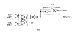
| JP6180450B2 (ja) * | 2015-02-02 | 2017-08-16 | キヤノン株式会社 | 制御装置、制御装置の制御方法及びプログラム |
| KR20160133073A (ko) | 2015-05-11 | 2016-11-22 | 에스케이하이닉스 주식회사 | 초기화 동작을 수행하는 반도체장치 및 반도체시스템 |
| KR102373544B1 (ko) * | 2015-11-06 | 2022-03-11 | 삼성전자주식회사 | 요청 기반의 리프레쉬를 수행하는 메모리 장치, 메모리 시스템 및 메모리 장치의 동작방법 |
| KR102535182B1 (ko) * | 2016-07-27 | 2023-05-23 | 에스케이하이닉스 주식회사 | 반도체 장치 |
| KR20220168520A (ko) * | 2021-06-16 | 2022-12-23 | 에스케이하이닉스 주식회사 | 리프레쉬 동작 주기를 조절하는 전자장치 |
Family Cites Families (3)
| Publication number | Priority date | Publication date | Assignee | Title |
|---|---|---|---|---|
| JP4246971B2 (ja) * | 2002-07-15 | 2009-04-02 | 富士通マイクロエレクトロニクス株式会社 | 半導体メモリ |
| JP4848564B2 (ja) | 2005-09-29 | 2011-12-28 | 株式会社ハイニックスセミコンダクター | 半導体メモリ装置のリセット制御回路 |
| KR100802074B1 (ko) * | 2006-09-08 | 2008-02-12 | 주식회사 하이닉스반도체 | 리프레쉬명령 생성회로를 포함하는 메모리장치 및리프레쉬명령 생성방법. |
-
2011
- 2011-08-01 JP JP2011168083A patent/JP2012123889A/ja not_active Abandoned
- 2011-11-02 US US13/287,600 patent/US8750067B2/en not_active Expired - Fee Related
Also Published As
| Publication number | Publication date |
|---|---|
| US20120127817A1 (en) | 2012-05-24 |
| US8750067B2 (en) | 2014-06-10 |
Similar Documents
| Publication | Publication Date | Title |
|---|---|---|
| CN100578665C (zh) | 半导体存储器 | |
| KR100885988B1 (ko) | 반도체 메모리 | |
| US8767497B2 (en) | Semiconductor device performing self refresh operation | |
| US8036060B2 (en) | Semiconductor device in which a memory array is refreshed based on an address signal | |
| CN101154435B (zh) | 半导体存储器及系统 | |
| JP2010170596A (ja) | 半導体記憶装置 | |
| US6834021B2 (en) | Semiconductor memory having memory cells requiring refresh operation | |
| JP2982928B2 (ja) | 半導体記憶装置 | |
| KR100899517B1 (ko) | 반도체 기억 장치 | |
| JP2012123889A (ja) | 半導体装置 | |
| US20130003482A1 (en) | Self-refresh control circuit and memory including the same | |
| TWI296804B (en) | Voltage generation control circuit in semiconductor memory device and method thereof | |
| US7548468B2 (en) | Semiconductor memory and operation method for same | |
| JP4428319B2 (ja) | 半導体記憶装置およびバンク・リフレッシュ方法 | |
| CN111326188B (zh) | 用于半导体存储器中的刷新操作的设备和方法 | |
| JP2006146992A (ja) | 半導体メモリ装置 | |
| KR102165736B1 (ko) | 반도체 메모리 장치 및 그 동작방법 | |
| JP2004185686A (ja) | 半導体記憶装置 | |
| TWI773203B (zh) | 半導體記憶體裝置 | |
| US6721224B2 (en) | Memory refresh methods and circuits | |
| JP4996094B2 (ja) | 半導体記憶装置及びそのリフレッシュ方法 | |
| US20050088894A1 (en) | Auto-refresh multiple row activation | |
| US20070297258A1 (en) | Semiconductor memory device and self-refresh method therefor | |
| JP2009059419A (ja) | 半導体記憶装置 |
Legal Events
| Date | Code | Title | Description |
|---|---|---|---|
| A711 | Notification of change in applicant |
Free format text: JAPANESE INTERMEDIATE CODE: A711 Effective date: 20130730 |
|
| A521 | Request for written amendment filed |
Free format text: JAPANESE INTERMEDIATE CODE: A523 Effective date: 20130822 |
|
| A621 | Written request for application examination |
Free format text: JAPANESE INTERMEDIATE CODE: A621 Effective date: 20140731 |
|
| A521 | Request for written amendment filed |
Free format text: JAPANESE INTERMEDIATE CODE: A523 Effective date: 20140827 |
|
| A762 | Written abandonment of application |
Free format text: JAPANESE INTERMEDIATE CODE: A762 Effective date: 20150203 |