JP2011237405A - Probe block and probe unit for inspection of display panel - Google Patents
Probe block and probe unit for inspection of display panel Download PDFInfo
- Publication number
- JP2011237405A JP2011237405A JP2011005256A JP2011005256A JP2011237405A JP 2011237405 A JP2011237405 A JP 2011237405A JP 2011005256 A JP2011005256 A JP 2011005256A JP 2011005256 A JP2011005256 A JP 2011005256A JP 2011237405 A JP2011237405 A JP 2011237405A
- Authority
- JP
- Japan
- Prior art keywords
- probe
- block
- film
- signal line
- display panel
- Prior art date
- Legal status (The legal status is an assumption and is not a legal conclusion. Google has not performed a legal analysis and makes no representation as to the accuracy of the status listed.)
- Pending
Links
Images


Classifications
-
- G—PHYSICS
- G01—MEASURING; TESTING
- G01R—MEASURING ELECTRIC VARIABLES; MEASURING MAGNETIC VARIABLES
- G01R1/00—Details of instruments or arrangements of the types included in groups G01R5/00 - G01R13/00 and G01R31/00
- G01R1/02—General constructional details
- G01R1/06—Measuring leads; Measuring probes
- G01R1/067—Measuring probes
- G01R1/073—Multiple probes
- G01R1/07307—Multiple probes with individual probe elements, e.g. needles, cantilever beams or bump contacts, fixed in relation to each other, e.g. bed of nails fixture or probe card
- G01R1/0735—Multiple probes with individual probe elements, e.g. needles, cantilever beams or bump contacts, fixed in relation to each other, e.g. bed of nails fixture or probe card arranged on a flexible frame or film
-
- G—PHYSICS
- G01—MEASURING; TESTING
- G01R—MEASURING ELECTRIC VARIABLES; MEASURING MAGNETIC VARIABLES
- G01R3/00—Apparatus or processes specially adapted for the manufacture or maintenance of measuring instruments, e.g. of probe tips
-
- G—PHYSICS
- G01—MEASURING; TESTING
- G01R—MEASURING ELECTRIC VARIABLES; MEASURING MAGNETIC VARIABLES
- G01R31/00—Arrangements for testing electric properties; Arrangements for locating electric faults; Arrangements for electrical testing characterised by what is being tested not provided for elsewhere
- G01R31/28—Testing of electronic circuits, e.g. by signal tracer
- G01R31/2851—Testing of integrated circuits [IC]
- G01R31/2886—Features relating to contacting the IC under test, e.g. probe heads; chucks
- G01R31/2887—Features relating to contacting the IC under test, e.g. probe heads; chucks involving moving the probe head or the IC under test; docking stations
-
- G—PHYSICS
- G09—EDUCATION; CRYPTOGRAPHY; DISPLAY; ADVERTISING; SEALS
- G09G—ARRANGEMENTS OR CIRCUITS FOR CONTROL OF INDICATING DEVICES USING STATIC MEANS TO PRESENT VARIABLE INFORMATION
- G09G3/00—Control arrangements or circuits, of interest only in connection with visual indicators other than cathode-ray tubes
- G09G3/006—Electronic inspection or testing of displays and display drivers, e.g. of LED or LCD displays
Landscapes
- Physics & Mathematics (AREA)
- General Physics & Mathematics (AREA)
- Engineering & Computer Science (AREA)
- Computer Hardware Design (AREA)
- Microelectronics & Electronic Packaging (AREA)
- General Engineering & Computer Science (AREA)
- Measuring Leads Or Probes (AREA)
- Liquid Crystal (AREA)
Abstract
Description
本発明は、ディスプレーパネル検査用プローブブロック及びプローブユニットに関するものである。 The present invention relates to a probe block for inspection of a display panel and a probe unit.
LCD(Liquid Crystal Display)生産工程は、ディスプレーパネルを作るセル(cell)工程と、ドライバー(driver)、バックライト(back light)、導光板及び偏光板をセル工程で生産されたディスプレーパネルと組立てて完成品を作り出すモジュール(module)組み立て工程とに大別される。 The LCD (Liquid Crystal Display) production process consists of a cell process for making a display panel, and a driver, backlight, light guide plate and polarizing plate are assembled with the display panel produced in the cell process. It is roughly divided into the module assembly process that produces finished products.
ここで、ディスプレーパネルは、ソース電極及びゲート電極がそれぞれ形成されている面を基板上に対向して配置した画像表示装置であって、基板間に液晶物質を入れ込んだ後、両電極に電圧を印加して電場を発生させ、この発生された電場によって液晶分子を動かして光の透過率を変化させることで画像を表現する。 Here, the display panel is an image display device in which the surfaces on which the source electrode and the gate electrode are formed are arranged facing each other on the substrate, and after the liquid crystal material is put between the substrates, the voltage is applied to both electrodes. Is applied to generate an electric field, and liquid crystal molecules are moved by the generated electric field to change the light transmittance, thereby expressing an image.
この時、ディスプレー検査用プローブユニット(以下、「プローブユニット」という。)は、セル工程で生産されたディスプレーパネルに対する検査を行うことで、製造工程で発生し得る欠陥の有無を確認する。 At this time, a display inspection probe unit (hereinafter referred to as a “probe unit”) performs an inspection on the display panel produced in the cell process, thereby confirming the presence or absence of a defect that may occur in the manufacturing process.
例えば、プローブユニットは、TFT(Thin Film Transistor)、TN(Twisted Nematic)、STN(Super Twisted Nematic)、CSTN(Color Super Twisted Nematic)、DSTN(Double Super Twisted Nematic)、有機EL(Electro Luminescence)などのディスプレーパネルの電極(またはパッド)にテスト用電気信号を印加して、該当ディスプレーパネルがピクセルエラー(pixel error)を起こさず正常に作動するか否かを検査する。 For example, the probe unit includes TFT (Thin Film Transistor), TN (Twisted Nematic), STN (Super Twisted Nematic), CSTN (Color Super Twisted Nematic), DSTN (Double Super Twisted Nematic), and organic EL (Electro Luminescence). A test electrical signal is applied to the electrode (or pad) of the display panel to check whether the display panel operates normally without causing a pixel error.
図1は、ディスプレーパネルを検査するための従来のプローブユニットの全体構成図である。 FIG. 1 is an overall configuration diagram of a conventional probe unit for inspecting a display panel.
図1に示すように、プローブユニット10は、ディスプレーパネル20に位置して各セルの異常有無を検査する。この時、プローブユニット10は、電気信号をディスプレーパネル20の電極に印加し、それによる出力信号を受けて検査システムに伝達する。
As shown in FIG. 1, the
このような過程を通じて、製造工程で発生し得るディスプレーパネル20の点欠陥、線欠陥、染み欠陥などの欠陥有無を検査する。
Through such a process, the
図2は、従来のプローブユニットの斜視図である。 FIG. 2 is a perspective view of a conventional probe unit.
図2に示すように、上述のプローブユニット10は、一般的にプローブブロック12、PCB部16、及びヘッドブロック14を含む。
As shown in FIG. 2, the
プローブブロック12は、ディスプレーパネル20の電極にプローブを接触させ、電気信号を印加し、それによる出力信号を検出して検査工程を行う。ここで、プローブブロック12は、TCP(Taped Carrier Package)ブロック(図示せず)と一体に形成されることができ、このようなTCPブロックは、PCB部16から受信した電気信号をプローブブロック12に伝達する。
The
ヘッドブロック14は、プローブブロック12のプローブが適当な物理的圧力でディスプレーパネル20の電極と接触するように、プローブブロック12を上下に移動させたり、一定の位置に固定させる。
The
PCB部16は、ディスプレーパネル20の各セルの検査のための電気信号を生成し、フィルム18を媒介にしてプローブブロック12に伝達する。
The
一方、最近は、高画質のディスプレーパネルが持続的に増加しつつあり、それによって高密度のディスプレーパネルを検査するためのプローブを具備したプローブブロックの必要性が大きくなっている。 On the other hand, recently, the number of high-quality display panels has been continuously increasing, and as a result, the need for a probe block having a probe for inspecting a high-density display panel has increased.
しかし、上述の従来のプローブブロックに構成されたプローブの径は、少なくとも300マイクロメートル程度であるため、高密度に微細電極が配列されたディスプレーパネルを検査するのに限界があった。特に、プローブを加工する技術的な限界によって均一かつ正確に配列されたプローブを具備した高密度のプローブブロックを作るのは困難であった。 However, since the diameter of the probe configured in the above-described conventional probe block is at least about 300 micrometers, there is a limit to inspecting a display panel in which fine electrodes are arranged at high density. In particular, it has been difficult to produce a high-density probe block having uniformly and accurately arranged probes due to technical limitations in processing the probes.
また、従来のプローブブロックに構成されたプローブの場合、プローブの先端部がディスプレーパネルに接触する時にプローブに摩耗が生じて、ディスプレーパネルに対する検査が正確に行われなかったり、適時にプローブを交換しなければならないという不便があった。そして、プローブの個別的な上下運動により、ピンミス(pin miss)が発生することもあった。 In addition, in the case of a probe configured with a conventional probe block, the probe is worn when the tip of the probe contacts the display panel, and the display panel is not accurately inspected, or the probe is replaced at an appropriate time. There was an inconvenience of having to. In addition, a pin miss may occur due to the individual vertical movement of the probe.
本発明の一実施例は、フォトリソグラフィ(photolithography)法を用いてプローブ部を高密度でかつ均一に一括して形成することにより、高密度に微細電極が配列されたディスプレーパネルを効果的に検査することができ、また、プローブ部の流動性がないため検査工程中のピンミスを減少させることができる、ディスプレーパネル検査用プローブブロック及びプローブユニットを提供することを目的としている。 One embodiment of the present invention effectively inspects a display panel in which fine electrodes are arranged at a high density by forming the probe portions at a high density and uniformly using a photolithography method. It is another object of the present invention to provide a display panel inspection probe block and a probe unit that can reduce pin mistakes during an inspection process because the probe portion does not have fluidity.
また、本発明の一実施例は、摩耗したコンタクトバンプから次のコンタクトバンプにコンタクト位置が変更されるように、複数個のコンタクトバンプをそれぞれの信号ラインに従ってプローブ部に一括して形成することにより、摩耗したコンタクトバンプを交換せずに次のコンタクトバンプを用いてディスプレーパネルに対する検査工程を持続的に行うことができる、ディスプレーパネル検査用プローブブロック及びプローブユニットを提供することを目的としている。 Also, in one embodiment of the present invention, a plurality of contact bumps are collectively formed on the probe portion according to each signal line so that the contact position is changed from the worn contact bump to the next contact bump. An object of the present invention is to provide a display panel inspection probe block and a probe unit that can continuously perform an inspection process for a display panel using the next contact bump without replacing the worn contact bump.
また、本発明の一実施例は、互いに違う長さを有する複数個の信号ライン部を交互に一定間隔毎に配列することにより、高電圧差によって発生し得る電気信号の干渉を最小化することができる、ディスプレーパネル検査用プローブブロック及びプローブユニットを提供することを目的としている。 Also, according to an embodiment of the present invention, a plurality of signal line portions having different lengths are alternately arranged at regular intervals, thereby minimizing the interference of electrical signals that may be caused by a high voltage difference. It is an object to provide a probe block and a probe unit for inspecting a display panel.
また、本発明の一実施例は、プローブフィルムを付着した第2のプレートの上端に接触する第1のプレートを具備することにより、プローブフィルムのコンタクトバンプを適当な物理的圧力で効果的にディスプレーパネルの電極に接触させることができる、ディスプレーパネル検査用プローブブロック及びプローブユニットを提供することを目的としている。 Also, an embodiment of the present invention includes a first plate that contacts the upper end of the second plate to which the probe film is attached, so that the contact bumps of the probe film can be effectively displayed at an appropriate physical pressure. An object of the present invention is to provide a probe block and a probe unit for inspecting a display panel, which can be brought into contact with the electrode of the panel.
上述の技術的課題を解決するための技術的手段として、本発明の第1の側面によるディスプレーパネル検査用プローブブロックは、傾斜突出部を含むプローブブロック本体部と、傾斜突出部の下側面に結合され、傾斜突出部の先端から突出して延長され、ディスプレーパネルの電極に接触して該電極に信号を印加するプローブフィルムと、傾斜突出部の上側面に結合され、突出して延長されたプローブフィルムの上部面と接触してプローブフィルムを支持する第1のプレートとを含む。 As a technical means for solving the above technical problem, a display panel inspection probe block according to the first aspect of the present invention is coupled to a probe block body including an inclined protrusion and a lower surface of the inclined protrusion. A probe film that protrudes and extends from the tip of the inclined protrusion, applies a signal to the electrode of the display panel, and a probe film that is coupled to the upper side of the inclined protrusion and extends A first plate in contact with the upper surface and supporting the probe film.
本発明の第2の側面によるディスプレーパネル検査用プローブユニットは、傾斜突出部を含むプローブブロック本体部、傾斜突出部の下側面に結合され、傾斜突出部の先端から突出して延長され、ディスプレーパネルの電極に接触して該電極に信号を印加するプローブフィルム、及び傾斜突出部の上側面に結合され、突出して延長されたプローブフィルムの上部面と接触してプローブフィルムを支持する第1のプレートを含むプローブブロックと、プローブブロックの上部に結合され、プローブフィルムとディスプレーパネルの電極が接触するようにプローブブロックを上下に移動させるヘッドブロックと、プローブブロックの下部に着脱可能に結合された圧着ブロックとを含む。 The display panel inspection probe unit according to the second aspect of the present invention is coupled to a probe block main body including an inclined protrusion and a lower surface of the inclined protrusion, and extends and protrudes from the tip of the inclined protrusion. A probe film that contacts the electrode and applies a signal to the electrode, and a first plate that supports the probe film by contacting the upper surface of the probe film that is coupled to the upper surface of the inclined projecting portion and extends. A probe block that is coupled to the upper part of the probe block, moves the probe block up and down so that the probe film and the electrode of the display panel are in contact with each other, and a crimping block that is detachably coupled to the lower part of the probe block including.
前述の本発明の課題解決手段によれば、フォトリソグラフィ法を用いて、プローブ部が高密度でかつ均一に一括して形成されるので、高密度に微細電極が配列されたディスプレーパネルを効果的に検査することができ、また、プローブ部の流動性がないため検査工程中のピンミスを減少させることができる。 According to the problem-solving means of the present invention described above, the photolithography method is used to form the probe portion at a high density and uniformly at the same time, so that a display panel in which fine electrodes are arranged at a high density is effective. In addition, since there is no fluidity of the probe portion, pin mistakes during the inspection process can be reduced.
また、前述の本発明の課題解決手段によれば、摩耗したコンタクトバンプから次のコンタクトバンプにコンタクト位置が変更されるように、複数個のコンタクトバンプがそれぞれの信号ラインに従ってプローブ部に一括して形成されるので、摩耗したコンタクトバンプを交換せずに次のコンタクトバンプを用いてディスプレーパネルに対する検査工程を持続的に行うことができる。 Further, according to the problem solving means of the present invention described above, a plurality of contact bumps are collectively placed on the probe portion according to each signal line so that the contact position is changed from the worn contact bump to the next contact bump. Since it is formed, the inspection process for the display panel can be continuously performed using the next contact bump without replacing the worn contact bump.
また、前述の本発明の課題解決手段によれば、互いに違う長さを有する複数個の信号ライン部が交互に一定間隔毎に配列されるので、高電圧差によって発生し得る電気信号の干渉を最小化することができる。 In addition, according to the problem solving means of the present invention described above, since a plurality of signal line portions having different lengths are alternately arranged at regular intervals, the interference of electrical signals that may occur due to a high voltage difference is prevented. Can be minimized.
また、前述の本発明の課題解決手段によれば、プローブフィルムを付着した第2のプレートの上端に接触する第1のプレートを具備しているので、プローブフィルムのコンタクトバンプを適当な物理的圧力で効果的にディスプレーパネルの電極に接触させることができる。 Further, according to the problem solving means of the present invention described above, since the first plate is in contact with the upper end of the second plate to which the probe film is attached, the contact bumps of the probe film are applied with an appropriate physical pressure. Can effectively contact the electrodes of the display panel.
以下では、添付した図面を参照して、本発明が属する技術分野において通常の知識を持った者が容易に実施することができるように本発明の実施例を詳しく説明する。但し、本発明は、様々な相異した形態に具現されることができ、ここで説明する実施例に限定されない。また、図面で本発明を明確に説明するための説明と関係ない部分は省略し、明細書全体に亘って類似している部分に対しては同様の図面符号を付けた。 Hereinafter, embodiments of the present invention will be described in detail with reference to the accompanying drawings so that a person having ordinary knowledge in the technical field to which the present invention belongs can be easily implemented. However, the present invention can be embodied in various different forms and is not limited to the embodiments described herein. Further, parts not related to the description for clearly explaining the present invention in the drawings are omitted, and like parts are denoted by like reference numerals throughout the specification.
明細書全体で、ある部分が他の部分と「連結」されている場合、これは「直接的に連結」されている場合だけではなく、その中間に他の素子を置いて「電気的に連結」されている場合も含む。また、ある部分がどの構成要素を「含む」場合、これは特別に反対される記載がない限り、他の構成要素を除くのではなく他の構成要素をさらに含むことができることを意味する。 Throughout the specification, when one part is “coupled” to another, this is not only “directly coupled”, but “electrically coupled” with other elements in between. "Is included. Also, where a part “includes” any component, this means that other components may be included rather than other components, unless specifically stated to the contrary.
図3は、本発明の一実施例によるプローブユニットを示す図である。図4a〜図4cは、プローブブロックの先端部を示す。そして、図5は、図3のプローブユニットの分解斜視図である。 FIG. 3 shows a probe unit according to an embodiment of the present invention. 4a-4c show the tip of the probe block. FIG. 5 is an exploded perspective view of the probe unit of FIG.
図3〜図5に示すように、本発明のプローブユニット200は、ヘッドブロック210、プローブブロック220、及び圧着ブロック230を含む。
As shown in FIGS. 3 to 5, the
ヘッドブロック210は、プローブブロック220の上部に結合されてプローブブロック220のプローブ部が適当な物理的圧力でディスプレーパネルの電極と接触するようにプローブブロック220を上下に移動及び固定させる。
The
プローブブロック220は、傾斜突出部224を含むプローブブロック本体部222と、傾斜突出部224の下側面に結合され、傾斜突出部224の先端から突出して延長され、ディスプレーパネルの電極に接触して信号を印加するプローブフィルム100と、傾斜突出部224の上側面に結合され、突出して延長されたプローブフィルム100の上部面と接触してプローブフィルム100を支持する第1のプレート242とを含む。ここで、プローブブロック220は、第1のプレート242の上部面に結合され、第1のプレート242を固定して支持する固定ブロック250をさらに含むことができる。
The
より具体的には、図4aに示すように、プローブブロック220の先端部Aは、傾斜突出部224の下側面に結合される第2のプレート241と、第2のプレート241の下側面に結合され、ディスプレーパネルの電極に接触されて信号を印加するプローブフィルム100と、傾斜突出部224の上側面に結合され、第2のプレート241の上部面と接触して第2のプレートの先端部241−1を支持する第1のプレート242と、を含むことができる。この時、第1のプレート242の先端部242−1は、第2のプレート241の先端部241−1に傾いた角度で接触することができる。
More specifically, as shown in FIG. 4 a, the tip A of the
そして、図4bに示すように、他の実施例において、プローブブロック220の先端部A’は、傾斜突出部224の下側面とプローブフィルム100との間に上述の第2のプレート241が介在せず、プローブフィルム100が傾斜突出部224の下側面に結合されて傾斜突出部224の先端から突出して延長され、第1のプレート242の先端部242−2が突出して延長されたプローブフィルム100の上部面に並んで接触するように延長された形態で構成されることができる。
As shown in FIG. 4b, in another embodiment, the tip A ′ of the
また、図4cに示すように、他の実施例において、プローブブロック220の先端部A”は、第2のプレート241と第1のプレート242が一体に形成され、第2のプレート241の下側面にプローブフィルム100が結合した形態で構成されることもできる。
Further, as shown in FIG. 4c, in another embodiment, the tip A ″ of the
圧着ブロック230は、プローブブロック220の下部に着脱可能に結合される。圧着ブロック230は、プローブブロック220の下部に形成された窪み部に収容される圧着ブロック本体部231と、本体部231の一側に突出して形成される結合突出部232と、圧着ブロック本体部231の下部から結合突出部232の回りに延長され、結合突出部232の上部面でプローブフィルム100側に圧着して接続された連結フィルム233と、を含む。
The crimping
ここで、連結フィルム233は、ディスプレーパネルを検査する駆動IC(Drive Integrated Circuit)(図示せず)を実装したものである。このような駆動ICは、ディスプレーパネルの各電極に電気的信号を印加すると共に、出力を検出することでディスプレーパネルの不良有無に対する検査工程を行う。連結フィルム233は、チップオンフィルム(Chip On Film)に具現されることができる。
Here, the
以下、図6及び図7を通じて、上述のプローブフィルム100についてより具体的に説明する。
Hereinafter, the
図6は、本発明の一実施例によるプローブフィルムの斜視図である。図7は、図6のプローブフィルムの平面図である。 FIG. 6 is a perspective view of a probe film according to an embodiment of the present invention. FIG. 7 is a plan view of the probe film of FIG.
図6及び図7に示すように、ディスプレーパネル検査用プローブブロックに装着されるプローブフィルム100は、信号ライン部151及び前記信号ライン部151から突出して形成され、ディスプレーパネルに具備された複数個の電極に接触されるコンタクトバンプ152をそれぞれ含む複数個のプローブ部150の上部面にフィルム170が接合された形態である。
6 and 7, the
ここで、プローブ部150は、フォトリソグラフィ法を用いて一定間隔で一括して形成されたものである。
Here, the
そして、プローブ部150のコンタクトバンプ152は、ディスプレーパネルに具備された複数個の電極に接触する部分である。ここで、コンタクトバンプ152は、先端部153の幅(a’)が他の部分の幅より広く形成され、高さ(b’)が縦方向に減少するような非対称の菱形であることができる。すなわち、コンタクトバンプ152は縦方向の線(c’)と先端部153の幅方向の線(a’)が交差する点の高さ(b’)が一番大きく、縦方向に行くほど高さが減少する形であることができる。
The
そして、プローブ部150の信号ライン部151は、ディスプレーパネルに接触したコンタクトバンプ152を通じて電気信号をディスプレーパネルに印加し、それによる出力信号を検査システムに伝達する。このようなコンタクトバンプ152と信号ライン部151は、後述する図8の形態に配列されることができる。
Then, the
図8は、本発明の一実施例による一定パターンに形成された信号ライン部及び前記信号ライン部から突出して形成されたコンタクトバンプを示す図である。 FIG. 8 is a diagram illustrating signal line portions formed in a certain pattern according to an embodiment of the present invention and contact bumps formed protruding from the signal line portions.
図8に示すように、コンタクトバンプ152は、互いに違う長さを持った複数個の信号ライン部151a、151bに複数個突出して形成されることができる。ここで、信号ライン部151a、151bは、第1の長さに形成された第1の信号ライン部151aと、前記第1の信号ライン部151aより後退され、第1の信号ライン部151aより短い第2の長さに形成された第2の信号ライン部151bと、を含み、第1の信号ライン部151aと第2の信号ライン部151bは交互に配列されることができる。
As shown in FIG. 8, a plurality of contact bumps 152 may be formed to protrude from a plurality of
ここで、同じ長さの信号ライン部には同信号が伝達され、第1の長さに形成された信号ライン部151aと第2の長さに形成された信号ライン部151bとの電圧差が20V〜40Vであることができる。このように、それぞれの信号ライン部151a、151bが交互に一定間隔で配列されることで、その電圧差によって発生し得る電気信号の干渉を最小化することができる。
Here, the same signal is transmitted to the signal line portion having the same length, and a voltage difference between the
そして、コンタクトバンプ152が信号ライン部に複数個突出して形成されているため、摩耗したコンタクトバンプを交換する必要なく、次のコンタクトバンプを用いてディスプレーパネルに対する検査工程を効果的に行うことができる。 Since a plurality of contact bumps 152 project from the signal line portion, the inspection process for the display panel can be effectively performed using the next contact bump without the need to replace the worn contact bump. .
より具体的には、コンタクトバンプ152は、上述の非対称の菱形に形成され、摩耗したコンタクトバンプから次のコンタクトバンプにスムーズにコンタクトの位置が変更されることができ、それによって摩耗したコンタクトバンプを交換せずに次のコンタクトバンプを用いてディスプレーパネルに対する検査工程が持続的に行われる。
More specifically, the
また、上述のプローブ部150は、フォトリソグラフィ法を用いて一定間隔で一括して形成されたものであって、コンタクトバンプ及び信号ライン部が流動せず、均一かつ正確に配列されているため、ディスプレーパネルに対する検査を行う時にピンミスを減少させることができる。以下、図9を通じてプローブブロック用プローブフィルムの製造方法についてより具体的に説明する。
In addition, the above-described
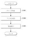
図9は、本発明の一実施例によるプローブブロック用プローブフィルムの製造方法の全体フロー図である。 FIG. 9 is an overall flowchart of a method for producing a probe block probe film according to an embodiment of the present invention.
図9に示すように、本発明のプローブブロック用プローブフィルムを製造するために、先ず信号ライン部及び前記信号ライン部から突出して形成されたコンタクトバンプをそれぞれ含む複数個のプローブ部150をフォトリソグラフィ法を用いて基板上に設定された間隔で一括して形成する(ステップS1001)。このステップS1001は後述するステップS1101〜S1108に対応している。
As shown in FIG. 9, in order to manufacture the probe block probe film of the present invention, first, a plurality of
次に、プローブ部150の上部面をフィルム部と接合する(ステップS1002)。このステップS1002は、後述するステップS1109〜S1110に対応している。
Next, the upper surface of the
そして、前記基板を除去する(ステップS1003)。このステップS1003は、後述するステップS1111に対応している。 Then, the substrate is removed (step S1003). This step S1003 corresponds to step S1111 described later.
上述の図9のプローブフィルムの製造方法のより具体的な工程及び詳細な製造順序に関しては、以下、図10及び図11a〜図11kを通じて後述する。 A more specific process and detailed manufacturing order of the method for manufacturing the probe film shown in FIG. 9 will be described later with reference to FIGS. 10 and 11a to 11k.
図10は、本発明の一実施例によるプローブブロック用プローブフィルムの製造方法の詳細フロー図である。そして、図11a〜図11kは、本発明の一実施例によるプローブブロック用プローブフィルムの製造方法を説明するための工程を示す図である。 FIG. 10 is a detailed flowchart of a method for manufacturing a probe block probe film according to an embodiment of the present invention. FIGS. 11a to 11k are diagrams illustrating steps for explaining a method for manufacturing a probe block probe film according to an embodiment of the present invention.
図11aに示すように、シリコーン(Si)基板110(以下、「基板」という。)上に形成された第1のフォトレジスト層120をパターニングして、一定の幅(c’)のパターンを形成する(ステップS1101)。ここで、該当幅(c’)はコンタクトバンプ152の長さに対応するように形成されることができる。より具体的には、予め定義されたマスク層を用いて紫外線露光装置などによって露光し、露光されたフォトレジスト層に現象工程を行ってマスクのパターンにより第1のフォトレジスト層120をパターニングすることができる。
As shown in FIG. 11a, the
次に、図11bに示すように、第1のフォトレジスト層120をマスクにし、基板110をエッチングしてコンタクトバンプ領域122を形成する(S1102)。より具体的には、DRIE(Deep silicon Reactive Ion Etching)工程を用いて第1のフォトレジスト層120をマスクにし、予め設定された深さで基板110をエッチングしてコンタクトバンプ領域122を形成することができる。
Next, as shown in FIG. 11B, using the
ここでDRIE工程は、例えば、ポリマー蒸着段階、ポリマーエッチング段階及びシリコーンエッチング段階順に行われることができる。そして、前記設定された深さは、コンタクトバンプ152の非対称の菱形に応じてその程度が異なることがある。すなわち縦方向の線(c’)と先端部の幅方向の線(a’)が交差する点が一番深くエッチングされる。これについては上述の図6及び図7を参照してほしい。
Here, the DRIE process may be performed in the order of, for example, a polymer deposition stage, a polymer etching stage, and a silicone etching stage. The set depth may vary depending on the asymmetric diamond shape of the
次に、図11cに示すように、コンタクトバンプ領域122を形成して露出した基板110の上部面と第1のフォトレジスト層120の上部面にシード層130を形成する(ステップS1103)。ここで、Ti(例えば、50nm)及びCu(例えば、100nm)シード金属をスパッタリングしてシード層130を形成することができる。より詳しくは、Tiをスパッタリングした後、Cuをスパッタリングする工程でシード層130を形成することができる。
Next, as shown in FIG. 11C, a
次に、図11dに示すように、シード層130の上部に第2のフォトレジスト層140をパターニングし、信号ライン部領域142を形成する(ステップS1104)。ここで、第2のフォトレジスト層140は信号ライン部領域142が形成されるように予め定義されたマスク層を用いて紫外線露光装置などによって露光し、露光されたフォトレジスト層に現象工程を行いマスクのパターンによってパターニングされることができる。
Next, as shown in FIG. 11d, the
次に、図11eに示すように、前記コンタクトバンプ領域122と信号ライン部領域142を導電性物質144で満たす(ステップS1105)。ここで、Ni、NiCo、NiFe及びNiWのうち、少なくとも一つの金属をメッキする工程でこのステップS1105が行われる。
Next, as shown in FIG. 11e, the
次に、図11fに示すように、導電性物質144で満たされた領域122、142の上部面を平坦化してプローブ部150を形成する(ステップS1106)。ここで、導電性物質144で満たされた領域122、142の上部面を化学的機械的研磨(CMP、Chemical Mechanical Polishing)工程で平坦化することができる。この時、プローブ部150の一端部151は信号ライン部に用いられ、一端部151から突出して形成された他端部152はコンタクトバンプに用いられる。
Next, as shown in FIG. 11f, the
次に、図11gに示すように、上述の第2のフォトレジスト層140を除去する(ステップS1107)。ここで、アッシング(ashing)工程、湿式除去工程、及びO2プラズマ方法のうち、何れか一つで第2のフォトレジスト層140を除去することができる。
Next, as shown in FIG. 11g, the
また、図11hに示すように、第2のフォトレジスト層140が除去されて露出したシード層131を除去する(ステップS1108)。ここで、乾式エッチングまたは湿式エッチング工程を通じて該当シード層131が除去されることができる。
Also, as shown in FIG. 11h, the
次に、図11iに示すように、プローブ部150の上部面に接着剤160を塗布する(ステップS1109)。この時、エポキシスプレディング(epoxy spreading)を行って接着剤160を塗布することができ、工程方法に応じて第1のフォトレジスト層120の上部面にも一括して接着剤160を塗布することができる。
Next, as shown in FIG. 11i, an adhesive 160 is applied to the upper surface of the probe unit 150 (step S1109). At this time, the adhesive 160 may be applied by performing epoxy spreading, and the adhesive 160 may be applied collectively to the upper surface of the
次に、図11jに示すように、接着剤160にフィルム部170を接合する(ステップS1110)。
Next, as shown in FIG. 11j, the
また、図11kに示すように、基板110を除去してプローブフィルムの製作を完了する(ステップS1111)。ここで、第1のフォトレジスト層120を共に除去することができる。この時、基板110及び第1のフォトレジスト層120を湿式エッチング工程で除去することができる。湿式エッチング工程はシリコーンをエッチングさせ得る条件のアルカリ溶液であるKOH溶液またはTMAH(tetramethyl ammonium hydroxide)溶液を使って行われることができる。そして、例えば、44wt%のKOH(potassium hydroxide)溶液を使って65℃の温度で湿式エッチングが行われることができる。また、湿式エッチング工程に使われるKOH溶液にイソプロフィルアルコールが添加されることができる。
Further, as shown in FIG. 11k, the
これと違って、DRIEなどの乾式エッチング工程により、基板110及び第1のフォトレジスト層120が除去されることもできる。
In contrast, the
この実施例では、基板110上に第1のフォトレジスト層120を形成及びパターニングした後、これをマスクにして基板110をエッチングすることで、コンタクトバンプ領域を形成したが、これとは違って、基板110上に複数個のフォトレジスト層を積み上げた後、基板110をエッチングせずに複数個のフォトレジスト層のみをエッチングすることで、コンタクトバンプ領域を形成することもできる。
In this embodiment, after forming and patterning the
このように硬い基板110をエッチングしないで、コンタクトバンプ領域を形成することで、工程の単純化及び製造原価の節減を図ることができる。
By forming the contact bump region without etching the
図12は、前記図11a〜図11kの工程で形成された信号ライン部及び前記信号ライン部から突出して形成された複数個のコンタクトバンプを示す図である。 FIG. 12 is a diagram illustrating a signal line portion formed in the steps of FIGS. 11a to 11k and a plurality of contact bumps formed to protrude from the signal line portion.
図12に示すように、上述の図11a〜図11kの工程で、信号ライン部151及び前記信号ライン部151から突出して形成された複数個のコンタクトバンプ152が一括して形成されることができる。この時、一つのコンタクトバンプ152が信号ライン部151から突出して形成されることもできる。
As shown in FIG. 12, the
一方、前述の本発明の説明は例示のためのものであり、本発明が属する技術分野の通常の知識を持った者は、本発明の技術的思想や必須的特徴を変更しなくても、他の具体的な形態に容易に変形することができる。よって、前述した実施例はすべての面において例示的なものであり、限定的なものではないことを理解するべきである。例えば、単一型に説明されている各構成要素は分散して実施されることもでき、これと同様に、分散したものと説明されている構成要素も結合した形態で実施されることができる。 On the other hand, the above description of the present invention is for illustrative purposes only, and those having ordinary knowledge in the technical field to which the present invention belongs can be used without changing the technical idea or essential features of the present invention. It can be easily transformed into other specific forms. Thus, it should be understood that the above-described embodiments are illustrative in all aspects and not limiting. For example, each component described in a single type can be implemented in a distributed manner, and similarly, components described as being distributed can be implemented in a combined form. .
また、本発明の範囲は、前記詳細な説明ではなく特許請求の範囲により表されるはずであり、特許請求の範囲の意味及び範囲、またその均等概念から導出される全ての変更または変形された形態が本発明の範囲に含まれるものと解釈するべきである。 The scope of the present invention should be expressed not by the above detailed description but by the scope of the claims, and all changes or modifications derived from the meaning and scope of the scope of claims and the equivalent concept thereof. It should be construed that the form is within the scope of the invention.
100 プローブフィルム
150 プローブ部
151 信号ライン部
152 コンタクトバンプ
170 フィルム部
200 プローブユニット
210 ヘッドブロック
220 プローブブロック
230 圧着ブロック
241 第2のプレート
242 第1のプレート
250 固定ブロック
DESCRIPTION OF
Claims (20)
傾斜突出部を含むプローブブロック本体部と、
前記傾斜突出部の下側面に結合され、前記傾斜突出部の先端から突出して延長され、ディスプレーパネルの電極に接触して前記電極に信号を印加するプローブフィルムと、
前記傾斜突出部の上側面に結合され、突出して延長された前記プローブフィルムの上部面と接触して、前記プローブフィルムを支持する第1のプレートと、
を含むことを特徴とするプローブブロック。 In the probe block for display panel inspection,
A probe block body including an inclined protrusion; and
A probe film coupled to a lower surface of the inclined protrusion, extending from a tip of the inclined protrusion, and contacting a display panel electrode to apply a signal to the electrode;
A first plate coupled to the upper side surface of the inclined projecting portion and contacting the upper surface of the projecting and extended probe film to support the probe film;
A probe block comprising:
信号ライン部及び前記信号ライン部から突出して形成され、前記ディスプレーパネルに具備された複数個の電極に接触するコンタクトバンプをそれぞれ含む複数個のプローブ部と、
前記プローブ部の上部面に接合されたフィルム部と、
を含むことを特徴とする請求項1に記載のプローブブロック。 The probe film is
A plurality of probe portions each including contact bumps that are formed to protrude from the signal line portion and the signal line portion and are in contact with the plurality of electrodes provided in the display panel;
A film part joined to the upper surface of the probe part;
The probe block according to claim 1, comprising:
前記第1の信号ライン部及び第2の信号ライン部が交互に配列されていることを特徴とする請求項6に記載のプローブブロック。 The signal line section includes a first signal line section formed to a first length, and a second signal line section formed to a second length shorter than the first signal line section. Including
The probe block according to claim 6, wherein the first signal line portions and the second signal line portions are alternately arranged.
傾斜突出部を含むプローブブロック本体部、前記傾斜突出部の下側面に結合され、前記傾斜突出部の先端から突出して延長され、ディスプレーパネルの電極に接触して前記電極に信号を印加するプローブフィルム、及び前記傾斜突出部の上側面に結合され、突出して延長された前記プローブフィルムの上部面と接触して、前記プローブフィルムを支持する第1のプレートを含むプローブブロックと、
前記プローブブロックの上部に結合され、前記プローブフィルムと前記ディスプレーパネルの電極が接触するように前記プローブブロックを上下に移動させるヘッドブロックと、
前記プローブブロックの下部に着脱可能に結合された圧着ブロックと、
を含むことを特徴とするプローブユニット。 In the probe unit for inspecting the display panel,
A probe block body including an inclined protrusion, a probe film coupled to a lower surface of the inclined protrusion, extending from the tip of the inclined protrusion, and contacting the electrode of the display panel to apply a signal to the electrode And a probe block including a first plate that supports the probe film in contact with an upper surface of the probe film that is coupled to the upper side surface of the inclined protrusion and protrudes and extends.
A head block that is coupled to the top of the probe block and moves the probe block up and down so that the probe film and the electrode of the display panel are in contact with each other;
A crimping block removably coupled to a lower portion of the probe block;
A probe unit comprising:
前記プローブブロックの下部に形成された窪み部に収容された圧着ブロック本体部と、
前記圧着ブロック本体部の一側に突出して形成された結合突出部と、
前記圧着ブロック本体部の下部から前記結合突出部の回りに延長され、前記結合突出部の上部面において前記プローブフィルム側に圧着して接続された連結フィルムと、
を含むことを特徴とする請求項10に記載のプローブユニット。 The crimp block is
A pressure-bonding block main body housed in a recess formed in the lower portion of the probe block;
A coupling protrusion formed to protrude from one side of the crimp block main body;
A connecting film that extends from the lower part of the crimping block main body around the coupling protrusion and is connected by crimping to the probe film side on the upper surface of the coupling protrusion,
The probe unit according to claim 10, comprising:
信号ライン部及び前記信号ライン部から突出して形成され、前記ディスプレーパネルに具備された複数個の電極に接触されるコンタクトバンプをそれぞれ含む複数個のプローブ部と、
前記プローブ部の上部面に接合されたフィルム部と、
を含むことを特徴とする請求項10に記載のプローブユニット。 The probe film is
A plurality of probe portions each including contact bumps that are formed to protrude from the signal line portion and the signal line portion and are in contact with the plurality of electrodes provided in the display panel;
A film part joined to the upper surface of the probe part;
The probe unit according to claim 10, comprising:
前記第1の信号ライン部及び第2の信号ライン部が交互に配列されていることを特徴とする請求項17に記載のプローブユニット。 The signal line part includes a first signal line part formed to a first length and a second signal line part formed to a second length shorter than the first signal line part,
The probe unit according to claim 17, wherein the first signal line portions and the second signal line portions are alternately arranged.
Applications Claiming Priority (2)
| Application Number | Priority Date | Filing Date | Title |
|---|---|---|---|
| KR1020100042231A KR101152181B1 (en) | 2010-05-06 | 2010-05-06 | Probe block for examining display panel and probe unit including thereor |
| KR10-2010-0042231 | 2010-05-06 |
Publications (1)
| Publication Number | Publication Date |
|---|---|
| JP2011237405A true JP2011237405A (en) | 2011-11-24 |
Family
ID=44886990
Family Applications (1)
| Application Number | Title | Priority Date | Filing Date |
|---|---|---|---|
| JP2011005256A Pending JP2011237405A (en) | 2010-05-06 | 2011-01-13 | Probe block and probe unit for inspection of display panel |
Country Status (3)
| Country | Link |
|---|---|
| JP (1) | JP2011237405A (en) |
| KR (1) | KR101152181B1 (en) |
| CN (1) | CN102236183A (en) |
Cited By (1)
| Publication number | Priority date | Publication date | Assignee | Title |
|---|---|---|---|---|
| CN104464586A (en) * | 2014-12-30 | 2015-03-25 | 京东方科技集团股份有限公司 | Display panel detection device and method |
Families Citing this family (6)
| Publication number | Priority date | Publication date | Assignee | Title |
|---|---|---|---|---|
| KR101311768B1 (en) * | 2012-06-15 | 2013-09-26 | 강기상 | Probe unit block |
| KR101964884B1 (en) * | 2012-06-29 | 2019-04-02 | 엘지디스플레이 주식회사 | Autoprobe unit and autoprobe apparatus using the same |
| KR101255111B1 (en) | 2012-10-25 | 2013-04-19 | 주식회사 프로이천 | Probe block and apparatus for testing panel having the same |
| KR101681652B1 (en) * | 2015-02-03 | 2016-12-01 | 주식회사 나노리퀴드디바이시스코리아 | Probe film for flat panel display test, probe block and probe unit comprising the same and method for fabricating the same |
| CN111158177B (en) * | 2020-02-28 | 2022-11-22 | 京东方科技集团股份有限公司 | Detection structure, display panel, detection device and detection system |
| KR102477553B1 (en) | 2021-01-22 | 2022-12-15 | 주식회사 디앤에스시스템 | Probe pin block for display panel test |
Citations (6)
| Publication number | Priority date | Publication date | Assignee | Title |
|---|---|---|---|---|
| JPH01122583A (en) * | 1987-11-05 | 1989-05-15 | Fujitsu Ltd | Measurement jig for semiconductor device |
| JPH0743384A (en) * | 1993-07-30 | 1995-02-14 | Nippon Avionics Co Ltd | Probe |
| JPH07321170A (en) * | 1994-05-23 | 1995-12-08 | Wentworth Lab Inc | Probe collection body for ic circuit testing instrument |
| JPH08110356A (en) * | 1994-10-11 | 1996-04-30 | Kobe Steel Ltd | Probe unit |
| JP2001337111A (en) * | 2000-05-30 | 2001-12-07 | Micronics Japan Co Ltd | Probe sheet and probe device using the same |
| JP2002040054A (en) * | 2000-07-25 | 2002-02-06 | Micronics Japan Co Ltd | Sheet-like electric connection device |
Family Cites Families (7)
| Publication number | Priority date | Publication date | Assignee | Title |
|---|---|---|---|---|
| JP2002148280A (en) * | 2000-11-08 | 2002-05-22 | Soushiyou Tec:Kk | Parallel loading unit of probe block for inspection |
| KR20060089968A (en) * | 2005-02-03 | 2006-08-10 | 주식회사 코디에스 | Probe unit for inspecting liquid crytal display panel |
| KR100720378B1 (en) * | 2005-04-13 | 2007-05-22 | 주식회사 코디에스 | Probe unit for inspecting liquid crytal display panel |
| KR100533193B1 (en) * | 2005-07-12 | 2005-12-08 | 프롬써어티 주식회사 | Probe unit for testing plat display pannel |
| KR100743427B1 (en) * | 2006-08-07 | 2007-07-30 | (주)오엘케이 | Apparatus for macro inspection of flat display panel |
| JP5209215B2 (en) * | 2007-01-17 | 2013-06-12 | 株式会社日本マイクロニクス | Probe unit and inspection device |
| JP2008275406A (en) * | 2007-04-27 | 2008-11-13 | Micronics Japan Co Ltd | Probe device and inspection device |
-
2010
- 2010-05-06 KR KR1020100042231A patent/KR101152181B1/en active IP Right Grant
-
2011
- 2011-01-13 JP JP2011005256A patent/JP2011237405A/en active Pending
- 2011-01-28 CN CN2011100316725A patent/CN102236183A/en active Pending
Patent Citations (6)
| Publication number | Priority date | Publication date | Assignee | Title |
|---|---|---|---|---|
| JPH01122583A (en) * | 1987-11-05 | 1989-05-15 | Fujitsu Ltd | Measurement jig for semiconductor device |
| JPH0743384A (en) * | 1993-07-30 | 1995-02-14 | Nippon Avionics Co Ltd | Probe |
| JPH07321170A (en) * | 1994-05-23 | 1995-12-08 | Wentworth Lab Inc | Probe collection body for ic circuit testing instrument |
| JPH08110356A (en) * | 1994-10-11 | 1996-04-30 | Kobe Steel Ltd | Probe unit |
| JP2001337111A (en) * | 2000-05-30 | 2001-12-07 | Micronics Japan Co Ltd | Probe sheet and probe device using the same |
| JP2002040054A (en) * | 2000-07-25 | 2002-02-06 | Micronics Japan Co Ltd | Sheet-like electric connection device |
Cited By (2)
| Publication number | Priority date | Publication date | Assignee | Title |
|---|---|---|---|---|
| CN104464586A (en) * | 2014-12-30 | 2015-03-25 | 京东方科技集团股份有限公司 | Display panel detection device and method |
| CN104464586B (en) * | 2014-12-30 | 2017-02-22 | 京东方科技集团股份有限公司 | Display panel detection device and method |
Also Published As
| Publication number | Publication date |
|---|---|
| CN102236183A (en) | 2011-11-09 |
| KR101152181B1 (en) | 2012-06-15 |
| KR20110122900A (en) | 2011-11-14 |
Similar Documents
| Publication | Publication Date | Title |
|---|---|---|
| JP2011237405A (en) | Probe block and probe unit for inspection of display panel | |
| JP2011237404A (en) | Probe film for probe block and manufacturing method of the same | |
| KR102248876B1 (en) | Array substrate for display device and displya device | |
| JP4430621B2 (en) | Probe for inspection of flat panel display device and method for manufacturing the same | |
| KR101155092B1 (en) | Method for probe film used probe block | |
| KR101272882B1 (en) | Probe film used probe block and method for manufacturing there of | |
| JP2006078319A (en) | Probe for inspection, inspection device, and method of manufacturing probe for inspection | |
| JP2011154024A (en) | Probe unit for inspecting micro pitch | |
| KR20110135574A (en) | Probe unit and method for fabricating the same | |
| KR20110121066A (en) | Method of manufacturing a flexible contact film used as probes of a probe unit | |
| KR100517729B1 (en) | Probe for manufacturing probe for testing flat pannel display, probe thereby, probe assembly having its | |
| KR100952138B1 (en) | Menufacturing method of probe assembly | |
| JPH07199219A (en) | Probe card for inspecting liquid crystal display device | |
| KR101174753B1 (en) | Thin film transistor, liquid crystal display and fabricating method the same | |
| JP5353919B2 (en) | Manufacturing method of liquid crystal panel | |
| KR101132574B1 (en) | Probe unit and method for fabricating the same | |
| KR100946373B1 (en) | Menufacturing method of probe assembly having drive ic | |
| KR100925496B1 (en) | Menufacturing method of probe assembly having drive ic | |
| KR101133092B1 (en) | Probe unit and method for fabricating the same | |
| KR100929649B1 (en) | Menufacturing method of probe assembly | |
| KR101279951B1 (en) | Apparatus for contact film and method for manufacturing the same | |
| KR100972758B1 (en) | Menufacturing method of probe assembly | |
| KR100914916B1 (en) | Probe Device And Fabricating Method Thereof | |
| KR101142462B1 (en) | Probe block with fine pitch tips for inspecting lcd panel and the fabrication method thereof | |
| KR101480681B1 (en) | Bump film, method for manufacturing of the bump film and probing apparatus having the bump film |
Legal Events
| Date | Code | Title | Description |
|---|---|---|---|
| A977 | Report on retrieval |
Free format text: JAPANESE INTERMEDIATE CODE: A971007 Effective date: 20121219 |
|
| A131 | Notification of reasons for refusal |
Free format text: JAPANESE INTERMEDIATE CODE: A131 Effective date: 20121226 |
|
| A02 | Decision of refusal |
Free format text: JAPANESE INTERMEDIATE CODE: A02 Effective date: 20130522 |