JP2011106973A - Contact probe, probe device, measurement device, and inspection device - Google Patents

Contact probe, probe device, measurement device, and inspection device Download PDF

Info

Publication number
JP2011106973A
JP2011106973A JP2009262433A JP2009262433A JP2011106973A JP 2011106973 A JP2011106973 A JP 2011106973A JP 2009262433 A JP2009262433 A JP 2009262433A JP 2009262433 A JP2009262433 A JP 2009262433A JP 2011106973 A JP2011106973 A JP 2011106973A
Authority
JP
Japan
Prior art keywords
probe
cylindrical body
probe pin
contact
columnar body
Prior art date
Legal status (The legal status is an assumption and is not a legal conclusion. Google has not performed a legal analysis and makes no representation as to the accuracy of the status listed.)
Granted
Application number
JP2009262433A
Other languages
Japanese (ja)
Other versions
JP5285579B2 (en
Inventor
Yoshinori Sato
義典 佐藤
Current Assignee (The listed assignees may be inaccurate. Google has not performed a legal analysis and makes no representation or warranty as to the accuracy of the list.)
Hioki EE Corp
Original Assignee
Hioki EE Corp
Priority date (The priority date is an assumption and is not a legal conclusion. Google has not performed a legal analysis and makes no representation as to the accuracy of the date listed.)
Filing date
Publication date
Application filed by Hioki EE Corp filed Critical Hioki EE Corp
Priority to JP2009262433A priority Critical patent/JP5285579B2/en
Publication of JP2011106973A publication Critical patent/JP2011106973A/en
Application granted granted Critical
Publication of JP5285579B2 publication Critical patent/JP5285579B2/en
Expired - Fee Related legal-status Critical Current
Anticipated expiration legal-status Critical

Links

Images

Landscapes

  • Tests Of Electronic Circuits (AREA)
  • Measuring Leads Or Probes (AREA)

Abstract

<P>PROBLEM TO BE SOLVED: To reduce measurement time, to simplify a circuit structure, to reduce the generation of operation failure, and to reliably establish connection to a probing object. <P>SOLUTION: The contact probe includes: a probe pin 21; a pillar body 22 having a spiral groove 44 and provided for the probe pin 21; a cylindrical body 23 that is movable in a state in which the pillar body 22 is inserted therethrough; a nonconductive ball 24a provided at the side of the base end part 51 of the cylindrical body 23, engaged with the spiral groove 44 in an insulated state, and pressing the spiral groove 44 in a direction for rotating the pillar body 22 with the movement of the cylindrical body 23; a conductive ball 24b connected to reference potential, provided at the side of a tip end part 52 of the cylindrical body 23, engaged with the spiral groove 44 in an electrically connected state when the cylindrical body 23 is located at the side of the base end part 41 of the pillar body 22, and separated from the spiral groove 44 when the cylindrical body 23 is located at the side of a tip end part 42 of the pillar body 22; and a spring 26 biasing the side of a tip end part 32 of the probe pin 21 in a direction separated from the cylindrical body 23. <P>COPYRIGHT: (C)2011,JPO&INPIT

Description

本発明は、プロービング対象体に蓄積されている電荷をプローブピンを介して放電する放電部を備えたコンタクトプローブ、そのコンタクトプローブを備えたプローブ装置、そのプローブ装置を備えた測定装置、およびその測定装置を備えた検査装置に関するものである。   The present invention relates to a contact probe including a discharge unit that discharges electric charges accumulated in a probing object through a probe pin, a probe device including the contact probe, a measuring device including the probe device, and a measurement thereof The present invention relates to an inspection apparatus including the apparatus.

この種のプローブ装置を備えた測定装置として、特開平10−142271号公報において出願人が開示したインサーキットテスタ(同公報の図4に開示したインサーキットテスタ)が知られている。このインサーキットテスタは、交流電圧源および交流電流計を有する計測部、被検査回路基板の各パターンにそれぞれ接触させられる複数のプローブピン、並びに各プローブピンと計測部とを接断するスキャナを備えて、各パターンについての静電容量を測定可能に構成されている。このインサーキットテスタを用いて上記の静電容量を測定する際には、共通電極の上に絶縁シートを載置し、その上に被検査回路基板を載置する。次いで、被検査回路基板の各パターンに各プローブピンをそれぞれ接触させる。続いて、スキャナによって各プローブピンの1つと計測部とを接続し、次いで、計測部の交流電圧源から出力される高位電圧をそのプローブピンを介してパターンに印加すると共に共通電極に低位電圧を印加する。続いて、パターンに流れる電流をプローブピンを介して入力し、交流電流計によってその電流値を測定する。次いで、交流電圧源から出力されるの電圧の電圧値と測定された電流値とに基づいてパターンと共通電極との間の静電容量を算出する。   An in-circuit tester disclosed by the applicant in Japanese Patent Application Laid-Open No. 10-142271 (in-circuit tester disclosed in FIG. 4 of the same publication) is known as a measuring apparatus provided with this type of probe device. This in-circuit tester includes a measurement unit having an AC voltage source and an AC ammeter, a plurality of probe pins that are brought into contact with each pattern of a circuit board to be inspected, and a scanner that connects and disconnects each probe pin and the measurement unit. The capacitance of each pattern can be measured. When measuring the capacitance using the in-circuit tester, an insulating sheet is placed on the common electrode, and a circuit board to be inspected is placed thereon. Next, each probe pin is brought into contact with each pattern of the circuit board to be inspected. Subsequently, one of the probe pins is connected to the measurement unit by the scanner, and then the high voltage output from the AC voltage source of the measurement unit is applied to the pattern via the probe pin and the low voltage is applied to the common electrode. Apply. Subsequently, the current flowing through the pattern is input via the probe pin, and the current value is measured by an AC ammeter. Next, the capacitance between the pattern and the common electrode is calculated based on the voltage value of the voltage output from the AC voltage source and the measured current value.

一方、この種の測定装置では、パターンに電圧を印加した際に被検査回路基板のパターンに蓄積された電荷が次のパターンについての静電容量の測定に影響を与えることがある。このため、この種の測定装置には、一般的に、静電容量の測定前または測定後(パターンに対する電圧の印加の前または後)において被検査回路基板のパターンに蓄積された電荷をパターンに接触させたプローブピンを介して放電(ディスチャージ)する放電部が備えられている。この場合、出願人が開示している上記のインサーキットテスタでは、プローブピンとグランド電位とを接断する放電用のスイッチが設けられており、このスイッチを作動させることで上記した電荷を放電可能に構成されている。   On the other hand, in this type of measuring apparatus, when a voltage is applied to the pattern, the charge accumulated in the pattern of the circuit board to be inspected may affect the measurement of the capacitance for the next pattern. For this reason, in this type of measuring apparatus, generally, the charge accumulated in the pattern of the circuit board to be inspected before or after the measurement of the capacitance (before or after the voltage is applied to the pattern) is used as the pattern. A discharge part is provided for discharging (discharging) through the contacted probe pin. In this case, the above-described in-circuit tester disclosed by the applicant is provided with a discharge switch for connecting and disconnecting the probe pin and the ground potential. By operating this switch, the above-described electric charge can be discharged. It is configured.

特開平10−142271号公報(第3−4頁、第4図)Japanese Patent Laid-Open No. 10-142271 (page 3-4, FIG. 4)

ところが、上記のインサーキットテスタには、改善すべき以下の課題がある。すなわち、上記のインサーキットテスタでは、放電用のスイッチを動作させることで被検査回路基板のパターンに蓄積された電荷を放電している。しかしながら、このインサーキットテスタでは、静電容量の測定前または測定後にスイッチ動作を行う必要があるため、例えば、数多くのパターンについての静電容量を測定する際には、スイッチ動作の回数も多くなり、その分、測定時間が長くなるという課題が存在する。また、このインサーキットテスタでは、放電用のスイッチを含む放電用の専用の回路が必要なため、その分、回路構成が複雑となるという課題も存在する。さらに、このインサーキットテスタでは、プローブピンとグランド電位とを接続する際(放電用のスイッチのオン動作時)に発生するスパークなどによって放電用のスイッチが動作不良を起こすおそれがあるという課題も存在する。また、この種のインサーキットテスタでは、パターンに対してプローブピンを押し付けることによって両者を接触させている。しかしながら、パターンに非導電性の酸化膜が形成されていることがあり、このようなときには、パターンに対してプローブピンを押し付けるだけでは、両者の接続(電気的接続)が完全に行われないことがある。したがって、上記のインサーキットテスタには、パターンに対するプローブピンの接続が不完全となることに起因して、放電が不十分となったり測定が不正確となったりするおそれがあるという課題も存在する。   However, the above in-circuit tester has the following problems to be improved. That is, in the above-described in-circuit tester, the electric charge accumulated in the pattern of the circuit board to be inspected is discharged by operating the discharge switch. However, in this in-circuit tester, it is necessary to perform the switch operation before or after the capacitance measurement. For example, when measuring the capacitance of many patterns, the number of switch operations increases. As a result, there is a problem that the measurement time becomes longer. In addition, since this in-circuit tester requires a dedicated circuit for discharging including a discharging switch, there is a problem that the circuit configuration becomes complicated accordingly. Further, in this in-circuit tester, there is a problem that the discharge switch may cause malfunction due to a spark or the like generated when the probe pin and the ground potential are connected (when the discharge switch is turned on). . In this type of in-circuit tester, the probe pins are pressed against the pattern to bring them into contact with each other. However, a non-conductive oxide film may be formed on the pattern. In such a case, the connection (electrical connection) between the two is not performed completely simply by pressing the probe pin against the pattern. There is. Therefore, the above-mentioned in-circuit tester also has a problem that there is a risk of insufficient discharge or inaccurate measurement due to incomplete connection of the probe pin to the pattern. .

本発明は、かかる改善すべき課題に鑑みてなされたものであり、測定時間の短縮、回路構成の簡素化、および動作不良の発生の低減を実現すると共に、プローブピンをプロービング対象体に対して確実に接続させ得るコンタクトプローブ、プローブ装置、測定装置および検査装置を提供することを主目的とする。   The present invention has been made in view of the problems to be improved, and realizes shortening of the measurement time, simplification of the circuit configuration, reduction of the occurrence of malfunction, and the probe pin with respect to the probing object. A main object is to provide a contact probe, a probe device, a measuring device, and an inspection device that can be reliably connected.

上記目的を達成すべく請求項1記載のコンタクトプローブは、プロービング対象に接触させられるプローブピンと、前記プロービング対象体に蓄積されている電荷を前記プローブピンを介して放電する放電処理を行う放電部とを備えたコンタクトプローブであって、前記放電部は、前記プローブピンよりも大径に形成されると共に外周面に螺旋部を有して当該プローブピンに電気的に接続された状態で当該プローブピンの基端部に配設された柱状体と、当該柱状体を挿通させた状態で前記プローブピンの軸線に沿って移動可能に配設された筒状体と、当該筒状体における基端部側の内面に配設されて前記螺旋部に対して絶縁された状態で係合して当該筒状体の移動に伴って前記柱状体を回転させる向きに前記螺旋部を押圧する第1係合部と、基準電位に接続されると共に前記筒状体における先端部側の内面に配設されて当該筒状体が前記柱状体の基端部側に位置しているときに前記螺旋部に対して電気的に接続された状態で係合し、かつ当該筒状体の移動に伴って柱状体を回転させる向きに前記螺旋部を押圧すると共に当該筒状体が当該柱状体の先端部側に位置しているときに当該螺旋部から離反して当該柱状体との電気的接続が解除される第2係合部と、前記プローブピンの前記先端部側を前記筒状体から離反させる向きに付勢する付勢部材とを備えて構成されている。   In order to achieve the above object, the contact probe according to claim 1 includes a probe pin that is brought into contact with a probing object, and a discharge unit that performs a discharge process for discharging the charge accumulated in the probing object through the probe pin. The discharge portion is formed with a diameter larger than that of the probe pin and has a spiral portion on the outer peripheral surface thereof and is electrically connected to the probe pin. A columnar body disposed at the base end of the tube, a cylindrical body disposed so as to be movable along the axis of the probe pin in a state where the columnar body is inserted, and a base end portion of the cylindrical body 1st engagement which is arrange | positioned in the state which is arrange | positioned on the inner surface of the side and is insulated with respect to the said spiral part, and presses the said spiral part in the direction which rotates the said columnar body with the movement of the said cylindrical body And It is connected to a quasi-potential and is disposed on the inner surface of the cylindrical body on the distal end side so that it is electrically connected to the spiral portion when the cylindrical body is located on the proximal end side of the columnar body. The cylindrical body is pressed in the direction of rotating the columnar body in accordance with the movement of the cylindrical body, and the cylindrical body is positioned on the distal end side of the columnar body. A second engagement portion that is separated from the spiral portion and is released from the columnar body when being in contact, and biased in a direction to separate the tip end side of the probe pin from the cylindrical body. And an urging member.

また、請求項2記載のコンタクトプローブは、請求項1記載のコンタクトプローブにおいて、前記第1係合部は、少なくとも外面が非導電性材料によって球状に形成されて前記筒状体に回転可能に配設された球状体で形成され、前記第2係合部は、少なくとも外面が導電性材料によって球状に形成されて前記筒状体に回転可能に配設された球状体で形成されている。   According to a second aspect of the present invention, in the contact probe according to the first aspect, the first engagement portion is arranged in a spherical shape with a non-conductive material at least on the outer surface so as to be rotatable on the cylindrical body. The second engaging portion is formed of a spherical body that is formed in a spherical shape with a conductive material and is rotatably disposed on the cylindrical body.

また、請求項3記載のプローブ装置は、請求項1または2記載のコンタクトプローブと、当該コンタクトプローブを移動させるプローブ移動機構とを備え、前記プローブ移動機構は、前記コンタクトプローブの前記筒状体が当該コンタクトプローブにおける前記柱状体の前記基端部側に位置している状態において当該筒状体を前記プロービング対象体に向けて移動させて当該プロービング対象体に当該コンタクトプローブの前記プローブピンを接触させるプロービング処理と、前記プロービング対象体に前記プローブピンを接触させている状態において前記コンタクトプローブにおける前記付勢部材の付勢力に抗して前記筒状体を前記柱状体の前記先端部側に向けて移動させて当該プローブピンを回転させる回転処理と、前記プローブピンを回転させている状態において前記付勢部材の付勢力に抗して前記筒状体を前記柱状体の前記先端部側に向けてさらに移動させて前記螺旋部から前記第2係合部を離反させる離反処理とを実行可能に構成されている。   According to a third aspect of the present invention, there is provided a probe device comprising: the contact probe according to the first or second aspect; and a probe moving mechanism for moving the contact probe, wherein the probe moving mechanism is configured such that the cylindrical body of the contact probe is In a state where the columnar body of the contact probe is positioned on the base end side, the cylindrical body is moved toward the probing object, and the probe pin of the contact probe is brought into contact with the probing object. In the state in which the probe pin is in contact with the probing object and the probing object, the cylindrical body is directed toward the tip side of the columnar body against the urging force of the urging member in the contact probe. Rotating process to rotate the probe pin and move the probe pin The cylindrical body is further moved toward the tip end side of the columnar body against the urging force of the urging member in a state of being rolled, and the second engaging portion is separated from the spiral portion. The separation processing can be executed.

また、請求項4記載の測定装置は、請求項3記載のプローブ装置と、前記プローブピンを介して入力した電気信号に基づいて前記プロービング対象体についての電気的物理量を測定する測定部とを備え、前記測定部は、前記第2係合部が前記螺旋部から離反している状態において前記電気的物理量を測定する。   According to a fourth aspect of the present invention, there is provided a measuring apparatus comprising: the probe apparatus according to the third aspect; and a measuring unit that measures an electrical physical quantity of the probing object based on an electric signal input via the probe pin. The measurement unit measures the electrical physical quantity in a state where the second engagement portion is separated from the spiral portion.

また、請求項5記載の検査装置は、請求項4記載の測定装置と、当該測定装置によって測定された前記電気的物理量に基づいて前記プロービング対象体を検査する検査部とを備えている。   An inspection apparatus according to a fifth aspect includes the measurement apparatus according to the fourth aspect and an inspection unit that inspects the probing object based on the electrical physical quantity measured by the measurement apparatus.

請求項1記載のコンタクトプローブ、請求項3記載のプローブ装置、請求項4記載の測定装置、および請求項5記載の検査装置では、プローブピン、柱状体、筒状体、第1係合部、第2係合部、および付勢部材を備えてコンタクトプローブが構成されている。この場合、コンタクトプローブが搭載されるプローブ装置におけるプローブ移動機構に対して、柱状体の基端部側に位置している筒状体をプロービング対象体に向けて移動させてプロービング対象体にプローブピンを接触させるプロービング処理と、プロービング対象体とプローブピンとの接触状態において筒状体を柱状体の先端部側に向けて移動させてプローブピンを回転させる回転処理と、プローブピンの回転状態において筒状体を柱状体の先端部側に向けてさらに移動させて螺旋部から第2係合部を離反させる離反処理とを実行させることで、このコンタクトプローブ、プローブ装置、測定装置および検査装置によれば、プロービング処理および回転処理の実行によって、プローブピン、柱状体、第2係合部および筒状体を介して、プロービング対象体に蓄積されている電荷を確実に放電させることができると共に、それに続いて離反処理を実行させることによってプロービング対象体についての電気的物理量の測定が可能な状態とさせることができる。したがって、このコンタクトプローブ、プローブ装置、測定装置および検査装置によれば、放電用のスイッチによって蓄積された電荷を放電する構成とは異なり、電気的物理量の測定前または測定後におけるスイッチ動作が不要なため、数多くのプロービング対象体についての電気的物理量を測定する際においても、スイッチ動作に要する時間分だけ測定時間を十分に短縮することができる。また、このコンタクトプローブ、プローブ装置、測定装置および検査装置によれば、柱状体、筒状体および第2係合部を備えて筒状体をグランド電位に接続するだけの簡易な構成であり、かつ放電用のスイッチを含む放電用の専用の回路が不要となるため、その分、回路構成を簡素化することができる。   In the contact probe according to claim 1, the probe device according to claim 3, the measuring device according to claim 4, and the inspection device according to claim 5, a probe pin, a columnar body, a cylindrical body, a first engagement portion, A contact probe is configured to include a second engagement portion and an urging member. In this case, with respect to the probe moving mechanism in the probe apparatus on which the contact probe is mounted, the cylindrical body located on the base end side of the columnar body is moved toward the probing target body, and the probe pin is attached to the probing target body. A probing process for contacting the probe body, a rotating process for rotating the probe pin by moving the cylindrical body toward the distal end side of the columnar body in the contact state between the probing object and the probe pin, and a cylindrical shape in the rotating state of the probe pin According to the contact probe, the probe device, the measuring device, and the inspection device, the body is further moved toward the distal end portion side of the columnar body and the separation process for separating the second engaging portion from the spiral portion is executed. By performing the probing process and the rotation process, the probe pin, the columnar body, the second engaging portion, and the cylindrical body are used to push the probe. The charge accumulated in Bingu subject it is possible to reliably discharge, can be electrically physical quantity of ready measurement for probing object by executing the separating process subsequently. Therefore, according to the contact probe, the probe device, the measurement device, and the inspection device, unlike the configuration in which the electric charge accumulated by the discharge switch is discharged, the switch operation before or after the measurement of the electrical physical quantity is unnecessary. Therefore, even when measuring the electrical physical quantities of a large number of probing objects, the measurement time can be sufficiently shortened by the time required for the switch operation. In addition, according to the contact probe, the probe device, the measuring device, and the inspection device, the columnar body, the cylindrical body, and the second engaging portion are simply configured to connect the cylindrical body to the ground potential. In addition, since a dedicated circuit for discharging including a discharging switch is not required, the circuit configuration can be simplified correspondingly.

さらに、このコンタクトプローブ、プローブ装置、測定装置および検査装置によれば、柱状体の螺旋部と第2係合部とが面的または線的に接触するように構成することで、両者の接触面積を十分に大きくすることができ、また、筒状体と第2係合部とが面的に接触するように構成することで、両者の接触面積を十分に大きくすることができるため、放電時におけるスパークの発生を低く抑えることができる結果、スパークの発生に起因する動作不良を十分に低減することができる。   Furthermore, according to the contact probe, the probe device, the measuring device, and the inspection device, the contact area between the spiral portion of the columnar body and the second engaging portion is configured to be in surface or linear contact. Since the cylindrical body and the second engaging portion are configured to be in surface contact with each other, the contact area between the two can be sufficiently increased. As a result of suppressing the occurrence of sparks at low, malfunction caused by the occurrence of sparks can be sufficiently reduced.

また、このコンタクトプローブ、プローブ装置、測定装置および検査装置によれば、コンタクトプローブが搭載されるプローブ装置におけるプローブ移動機構に対して、プロービング対象体とプローブピンとの接触状態において回転処理を実行させることで、例えば、プロービング対象体の表面に非導電性の酸化膜が形成されていたとしても、プローブピンが回転によってその酸化膜を貫通させて、プローブピンとプロービング対象体とを電気的に確実に接続させることができる。したがって、このコンタクトプローブ、プローブ装置、測定装置および検査装置によれば、プロービング対象体の表面に非導電性の酸化膜が形成されているときにおいても、そのプロービング対象体に蓄積されている電荷を確実に放電することができると共に、そのプロービング対象体についての電気的物理量を正確に測定することができる。   Further, according to the contact probe, the probe device, the measuring device, and the inspection device, the probe moving mechanism in the probe device on which the contact probe is mounted is caused to execute the rotation process in the contact state between the probing object and the probe pin. For example, even if a non-conductive oxide film is formed on the surface of the probing object, the probe pin penetrates the oxide film by rotation, and the probe pin and the probing object are electrically connected reliably. Can be made. Therefore, according to the contact probe, the probe device, the measuring device, and the inspection device, even when a non-conductive oxide film is formed on the surface of the probing target, the charge accumulated in the probing target is While being able to discharge reliably, the electrical physical quantity about the probing object can be accurately measured.

また、請求項2記載のコンタクトプローブ、請求項3記載のプローブ装置、請求項4記載の測定装置、および請求項5記載の検査装置によれば、第1係合部を球状に形成して筒状体に回転可能に配設し、第2係合部を球状に形成して筒状体に回転可能に配設したことにより、各係合部と柱状体の螺旋部との摩擦抵抗を十分に低減させることができる結果、柱状体およびプローブピンをスムーズに回転させることができる。   Further, according to the contact probe according to claim 2, the probe device according to claim 3, the measuring device according to claim 4, and the inspection device according to claim 5, the first engaging portion is formed in a spherical shape to form a cylinder. Since the second engaging portion is formed in a spherical shape and is rotatably arranged on the cylindrical body, the frictional resistance between each engaging portion and the spiral portion of the columnar body is sufficient. As a result, the columnar body and the probe pin can be smoothly rotated.

検査装置1の構成を示す構成図である。1 is a configuration diagram showing a configuration of an inspection apparatus 1. FIG. プローブピン21、柱状体22、筒状体23、非導電性ボール24a、導電性ボール24b、スプリング支持板25およびスプリング26の構成を示す構成図である。3 is a configuration diagram showing configurations of a probe pin 21, a columnar body 22, a cylindrical body 23, a non-conductive ball 24a, a conductive ball 24b, a spring support plate 25, and a spring 26. FIG. 検査装置1の動作を説明する第1の説明図である。FIG. 3 is a first explanatory view explaining the operation of the inspection apparatus 1. 検査装置1の動作を説明する第2の説明図である。FIG. 6 is a second explanatory diagram for explaining the operation of the inspection apparatus 1. 検査装置1の動作を説明する第3の説明図である。FIG. 6 is a third explanatory diagram for explaining the operation of the inspection apparatus 1. 検査装置1の動作を説明する第4の説明図である。FIG. 10 is a fourth explanatory diagram explaining the operation of the inspection apparatus 1.

以下、コンタクトプローブ、プローブ装置、測定装置および検査装置の実施の形態について、添付図面を参照して説明する。   Hereinafter, embodiments of a contact probe, a probe device, a measurement device, and an inspection device will be described with reference to the accompanying drawings.

最初に、検査装置1の構成について、図面を参照して説明する。図1に示す検査装置1は、同図に示す回路基板100における複数の導体パターン101(プロービング対象体の一例であって、同図では2つの導体パターン101のみを図示している)のうちの任意の一対の導体パターン101の間の静電容量Cm(電気的物理量の一例)を測定すると共に、その静電容量Cmに基づいて回路基板100の良否を検査可能に構成されている。具体的には、検査装置1は、同図に示すように、基板保持部11、プローブ装置12a、プローブ装置12b(以下、プローブ装置12a,12bを区別しないときには「プローブ装置12」ともいう)、測定用信号生成部13、測定部14および制御部15を備えて構成されている。なお、検査装置1を構成する各構成要素のうちの、検査機能を除く各機能を有する構成要素によって測定装置が構成される。具体的には、測定装置は、基板保持部11、プローブ装置12、測定用信号生成部13、測定部14、並びに制御部15のうちのプローブ装置12、測定用信号生成部13および測定部14を制御する機能を有する部分によって構成される。   First, the configuration of the inspection apparatus 1 will be described with reference to the drawings. The inspection apparatus 1 shown in FIG. 1 includes a plurality of conductor patterns 101 (an example of a probing object, in which only two conductor patterns 101 are shown) in the circuit board 100 shown in FIG. The capacitance Cm (an example of an electrical physical quantity) between any pair of conductor patterns 101 is measured, and the quality of the circuit board 100 can be inspected based on the capacitance Cm. Specifically, as shown in the figure, the inspection apparatus 1 includes a substrate holding unit 11, a probe apparatus 12a, and a probe apparatus 12b (hereinafter also referred to as “probe apparatus 12” when the probe apparatuses 12a and 12b are not distinguished), The measurement signal generation unit 13, the measurement unit 14, and the control unit 15 are provided. In addition, a measuring apparatus is comprised by the component which has each function except the test | inspection function among each component which comprises the test | inspection apparatus 1. FIG. Specifically, the measurement apparatus includes the substrate holding unit 11, the probe device 12, the measurement signal generation unit 13, the measurement unit 14, and the probe unit 12, the measurement signal generation unit 13, and the measurement unit 14 among the control units 15. It is comprised by the part which has the function to control.

基板保持部11は、保持板と、保持板に取り付けられて回路基板100の端部を挟み込んで固定するクランプ機構(いずれも図示せず)とを備えて、回路基板100を保持可能に構成されている。   The substrate holding unit 11 includes a holding plate and a clamp mechanism (none of which is shown) that is attached to the holding plate and sandwiches and fixes the end portion of the circuit substrate 100, and is configured to hold the circuit substrate 100. ing.

プローブ装置12a,12bは、図1,2に示すように、コンタクトプローブ71およびプローブ移動機構27をそれぞれ備えて構成されている。   As shown in FIGS. 1 and 2, each of the probe devices 12 a and 12 b includes a contact probe 71 and a probe moving mechanism 27.

コンタクトプローブ71は、プローブピン21、柱状体22、筒状体23、非導電性ボール24a、導電性ボール24b、スプリング支持板25およびスプリング26をそれぞれ備えて構成されている。なお、柱状体22、筒状体23、非導電性ボール24a、導電性ボール24b、スプリング支持板25およびスプリング26によって放電部が構成される。   The contact probe 71 includes a probe pin 21, a columnar body 22, a cylindrical body 23, a non-conductive ball 24a, a conductive ball 24b, a spring support plate 25, and a spring 26, respectively. The columnar body 22, the cylindrical body 23, the nonconductive ball 24 a, the conductive ball 24 b, the spring support plate 25 and the spring 26 constitute a discharge part.

プローブピン21は、図2に示すように、導電性を有する材料(例えば金属)によって断面が円形で先端が鋭利に形成されている。また、プローブピン21は、図外の導線を介して測定用信号生成部13および測定部14に接続されている。また、プローブピン21は、図2に示すように、検査処理の実行時において導体パターン101にプロービング(接触)させられる。   As shown in FIG. 2, the probe pin 21 has a circular cross section and a sharp tip formed of a conductive material (for example, metal). The probe pin 21 is connected to the measurement signal generator 13 and the measurement unit 14 via a lead wire (not shown). Further, as shown in FIG. 2, the probe pin 21 is probed (contacted) with the conductor pattern 101 when the inspection process is executed.

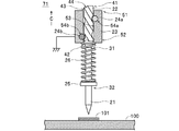
柱状体22は、図2に示すように、導電性を有する材料によってプローブピン21よりも大径の円柱状に形成されると共に、その外周面43に螺旋部の一例としての螺旋(らせん)状溝44を有して構成されている。この場合、螺旋溝44は、断面U字状に形成され、導電性ボール24bとの係合状態において、導電性ボール24bと面的または線的に接触する。また、柱状体22は、その軸線とプローブピン21の軸線とが同軸となるようにして、プローブピン21の基端部31に固定(配設)されてプローブピン21に電気的に接続されている。   As shown in FIG. 2, the columnar body 22 is formed in a cylindrical shape having a diameter larger than that of the probe pin 21 by using a conductive material, and a spiral shape as an example of a spiral portion on the outer peripheral surface 43 thereof. A groove 44 is provided. In this case, the spiral groove 44 is formed in a U-shaped cross section, and comes into surface contact or linear contact with the conductive ball 24b in the engaged state with the conductive ball 24b. The columnar body 22 is fixed (arranged) to the proximal end portion 31 of the probe pin 21 and electrically connected to the probe pin 21 so that the axis of the columnar body 22 and the axis of the probe pin 21 are coaxial. Yes.

筒状体23は、図2に示すように、導電性を有する材料によって柱状体22を挿通可能な円筒状(筒状の一例)に形成されている。また、筒状体23は、非導電性を有する絶縁層(図示せず)が内面53に形成されることにより、柱状体22に対して絶縁されている。また、筒状体23における先端部52側の内面53には、非導電性ボール24aを回転可能に保持する凹部54aが形成され、筒状体23における先端部52側の内面53には、導電性ボール24bを回転可能に保持する凹部54bが形成されている。この場合、凹部54bの内面には上記した絶縁層が設けられておらず、凹部54bの内面と導電性ボール24bとの間が電気的に接続可能となっている。また、筒状体23は、柱状体22を挿通させた状態でプローブピン21の軸線に沿って移動可能に配設されている。さらに、筒状体23は、図外の導線を介してグランド電位(基準電位)に接続されている。   As shown in FIG. 2, the cylindrical body 23 is formed in a cylindrical shape (an example of a cylindrical shape) through which the columnar body 22 can be inserted with a conductive material. Further, the cylindrical body 23 is insulated from the columnar body 22 by forming a non-conductive insulating layer (not shown) on the inner surface 53. Further, a concave portion 54a for rotatably holding the non-conductive ball 24a is formed on the inner surface 53 of the cylindrical body 23 on the distal end portion 52 side, and the inner surface 53 on the distal end portion 52 side of the cylindrical body 23 is electrically conductive. A recess 54b is formed for rotatably holding the conductive ball 24b. In this case, the above-described insulating layer is not provided on the inner surface of the recess 54b, and the inner surface of the recess 54b and the conductive ball 24b can be electrically connected. Further, the cylindrical body 23 is disposed so as to be movable along the axis of the probe pin 21 in a state where the columnar body 22 is inserted. Furthermore, the cylindrical body 23 is connected to a ground potential (reference potential) via a lead wire (not shown).

非導電性ボール24aは、第1係合部の一例であって、硬質の非導電性材料(例えば、セラミックス)によって球状に形成されている。また、非導電性ボール24aは、図2に示すように、筒状体23の凹部54aに嵌め込まれ(圧入され)て、凹部54aから離脱せず、かつ回転可能な状態で筒状体23に保持されている。また、非導電性ボール24aは、柱状体22の外周面43に形成されている螺旋状溝44に係合している。この場合、非導電性ボール24aは、非導電性を有しているため、螺旋状溝44(柱状体22)に対して絶縁されている。また、非導電性ボール24aは、筒状体23の移動に伴って螺旋状溝44の内壁を押圧し、これによって柱状体22(柱状体22が固定されているプローブピン21)を回転させる(図3,5参照)。   The non-conductive ball 24a is an example of a first engagement portion, and is formed in a spherical shape with a hard non-conductive material (for example, ceramic). Further, as shown in FIG. 2, the non-conductive ball 24a is fitted (press-fitted) into the concave portion 54a of the cylindrical body 23, and is not detached from the concave portion 54a and can be rotated in the cylindrical body 23. Is retained. Further, the non-conductive ball 24 a is engaged with a spiral groove 44 formed on the outer peripheral surface 43 of the columnar body 22. In this case, since the non-conductive ball 24a has non-conductivity, it is insulated from the spiral groove 44 (columnar body 22). Further, the nonconductive ball 24a presses the inner wall of the spiral groove 44 as the cylindrical body 23 moves, thereby rotating the columnar body 22 (the probe pin 21 to which the columnar body 22 is fixed) ( (See FIGS. 3 and 5).

導電性ボール24bは、第2係合部の一例であって、硬質の導電性材料(例えば、鉄)によって球状に形成されている。また、導電性ボール24bは、図2に示すように、筒状体23の凹部54bに嵌め込まれ(圧入され)て、凹部54bから離脱せず、かつ回転可能な状態で筒状体23に保持されている。この場合、導電性ボール24bは、自身が導電性を有し、かつ凹部54bの内面に絶縁層が設けられていないため、筒状体23に対して電気的に接続され、さらに筒状体23を介してグランド電位に接続される。また、導電性ボール24bは、凹部54bの内面に面的に接触しており、両者の接触面積が十分に大きくなっている。   The conductive ball 24b is an example of a second engagement portion, and is formed in a spherical shape with a hard conductive material (for example, iron). Further, as shown in FIG. 2, the conductive ball 24b is fitted (press-fitted) into the concave portion 54b of the cylindrical body 23 and is held in the cylindrical body 23 in a rotatable state without being detached from the concave portion 54b. Has been. In this case, since the conductive ball 24b itself has conductivity and no insulating layer is provided on the inner surface of the recess 54b, the conductive ball 24b is electrically connected to the cylindrical body 23, and further, the cylindrical body 23. To be connected to the ground potential. Further, the conductive ball 24b is in surface contact with the inner surface of the recess 54b, and the contact area between the two is sufficiently large.

また、導電性ボール24bは、図2に示すように、筒状体23が柱状体22の基端部41側に位置しているときには、柱状体22の螺旋状溝44に係合している。この場合、導電性ボール24bは、導電性を有しているため、この状態においては螺旋状溝44(柱状体22)に電気的に接続されている。また、導電性ボール24bは、筒状体23の移動に伴って螺旋状溝44の内壁を押圧し、非導電性ボール24aと共に柱状体22を回転させる。さらに、導電性ボール24bは、図4に示すように、筒状体23が柱状体22の先端部42側に位置しているときに、螺旋状溝44から離反して、柱状体22との電気的接続が解除される。   Further, as shown in FIG. 2, the conductive ball 24 b is engaged with the spiral groove 44 of the columnar body 22 when the cylindrical body 23 is positioned on the base end portion 41 side of the columnar body 22. . In this case, since the conductive ball 24b has conductivity, in this state, the conductive ball 24b is electrically connected to the spiral groove 44 (columnar body 22). The conductive ball 24b presses the inner wall of the spiral groove 44 as the cylindrical body 23 moves, and rotates the columnar body 22 together with the non-conductive ball 24a. Furthermore, as shown in FIG. 4, the conductive ball 24 b is separated from the spiral groove 44 when the cylindrical body 23 is positioned on the tip end portion 42 side of the columnar body 22, and The electrical connection is released.

スプリング支持板25は、図2に示すように、非導電性を有しかつ摩擦係数が小さい材料(一例として、PTFEなどのフッ素系樹脂)によって円板状に形成されている。また、スプリング支持板25は、中心部に形成された挿通孔にプローブピン21の先端部32側が挿通された状態で、プローブピン21に対して回転可能に配設されている(つまり、スプリング支持板25に対してプローブピン21が回転可能な状態となっている)。   As shown in FIG. 2, the spring support plate 25 is formed in a disc shape from a non-conductive material having a small friction coefficient (for example, a fluorine resin such as PTFE). The spring support plate 25 is disposed so as to be rotatable with respect to the probe pin 21 in a state where the distal end portion 32 side of the probe pin 21 is inserted into an insertion hole formed in the center (ie, spring support). The probe pin 21 is rotatable with respect to the plate 25).

スプリング26は、付勢部材の一例であって、図2に示すように、プローブピン21を挿通させた状態で筒状体23とスプリング支持板25との間に配設されている。また、スプリング26は、基端部が筒状体23の先端部52に固定されると共に、先端部がスプリング支持板25に固定されて、スプリング支持板25が配設されているプローブピン21の先端部32側を筒状体23から離反させる向きに付勢する。また、スプリング26は、表面に非導電性を有する絶縁層(図示せず)が形成されており、プローブピン21、柱状体22および筒状体23に対して絶縁されている。   The spring 26 is an example of an urging member, and is disposed between the cylindrical body 23 and the spring support plate 25 with the probe pin 21 inserted as shown in FIG. The spring 26 has a proximal end portion fixed to the distal end portion 52 of the cylindrical body 23, a distal end portion fixed to the spring support plate 25, and the probe pin 21 on which the spring support plate 25 is disposed. The tip 32 is biased in a direction to move away from the cylindrical body 23. The spring 26 has a non-conductive insulating layer (not shown) formed on the surface thereof, and is insulated from the probe pin 21, the columnar body 22, and the cylindrical body 23.

プローブ移動機構27は、コンタクトプローブ71をX−Y−Z方向に移動可能に構成されて、制御部15の制御に従って回路基板100の導体パターン101にプローブピン21の先端を接触(プロービング)させるプロービング処理を実行する。具体的には、プローブ移動機構27は、図1,2に示すように、スプリング26の付勢力によって筒状体23が柱状体22の基端部41側に位置している状態(以下、この状態を「初期状態」ともいう)のコンタクトプローブ71における筒状体23をアーム61で保持し、回路基板100の表面に沿った方向(X−Y方向)、および回路基板100に対して近接する向き(Z方向)にコンタクトプローブ71を移動させてプロービング処理を実行する。   The probe moving mechanism 27 is configured to be able to move the contact probe 71 in the X, Y, and Z directions, and performs probing that makes the tip of the probe pin 21 contact (probing) the conductor pattern 101 of the circuit board 100 under the control of the control unit 15. Execute the process. Specifically, as shown in FIGS. 1 and 2, the probe moving mechanism 27 is in a state where the cylindrical body 23 is positioned on the base end portion 41 side of the columnar body 22 by the urging force of the spring 26 (hereinafter, this The cylindrical body 23 of the contact probe 71 in a state (also referred to as “initial state”) is held by the arm 61 and is close to the circuit board 100 in the direction along the surface of the circuit board 100 (XY direction). The probing process is executed by moving the contact probe 71 in the direction (Z direction).

また、プローブ移動機構27は、回路基板100の導体パターン101にプローブピン21の先端を接触させている状態において、スプリング26による付勢力に抗して筒状体23を柱状体22の先端部42側(導体パターン101)に向けて(図3における矢印Aの向きに)移動させ、これによってプローブピン21を回転させる回転処理を実行する。   In addition, the probe moving mechanism 27 moves the cylindrical body 23 against the urging force of the spring 26 in a state where the tip of the probe pin 21 is in contact with the conductor pattern 101 of the circuit board 100. A rotation process is performed in which the probe pin 21 is rotated by moving toward the side (conductor pattern 101) (in the direction of arrow A in FIG. 3).

さらに、プローブ移動機構27は、プローブピン21を回転させている状態において(回転処理に連続して)、スプリング26による付勢力に抗して筒状体23を柱状体22の先端部42側に向けてさらに移動させて螺旋状溝44から導電性ボール24bを離反させる離反処理を実行する。   Further, the probe moving mechanism 27 moves the cylindrical body 23 toward the distal end portion 42 side of the columnar body 22 against the urging force of the spring 26 in a state where the probe pin 21 is rotated (continuous to the rotation process). A separation process is performed in which the conductive ball 24 b is separated from the spiral groove 44 by further moving toward the spiral groove 44.

また、プローブ移動機構27は、離反処理の実行後に、筒状体23を柱状体22の基端部41側に向けて移動させることで螺旋状溝44に導電性ボール24bを係合させて初期状態に復帰させる復帰処理を実行する。   In addition, the probe moving mechanism 27 engages the conductive ball 24b with the spiral groove 44 by moving the cylindrical body 23 toward the proximal end portion 41 side of the columnar body 22 after the separation process is performed. A return process for returning to the state is executed.

この場合、このプローブ装置12では、上記したように、導電性ボール24bが螺旋状溝44に係合している状態においては、導電性ボール24bが柱状体22に電気的に接続されている。また、導電性ボール24bは、筒状体23を介してグランド電位に接続されている。このため、導電性ボール24bが螺旋状溝44に係合している状態においては、柱状体22に電気的に接続されているプローブピン21が、柱状体22、導電性ボール24bおよび筒状体23を介してグランド電位に接続されている。また、このプローブ装置12では、回路基板100の導体パターン101にプローブピン21の先端を接触させている状態において回転処理が行われて、プローブピン21と導体パターン101との電気的接続が確実に行われる。したがって、このプローブ装置12では、プローブ移動機構27がプロービング処理および回転処理を実行することで、回路基板100の導体パターン101に電荷が蓄積されているときには、プローブピン21、柱状体22、導電性ボール24bおよび筒状体23を介して、その電荷が放電(ディスチャージ)される放電処理が静電容量Cmの測定前に行われる。   In this case, in the probe device 12, the conductive ball 24 b is electrically connected to the columnar body 22 in a state where the conductive ball 24 b is engaged with the spiral groove 44 as described above. In addition, the conductive ball 24 b is connected to the ground potential via the cylindrical body 23. Therefore, in a state where the conductive ball 24 b is engaged with the spiral groove 44, the probe pin 21 electrically connected to the columnar body 22 is connected to the columnar body 22, the conductive ball 24 b, and the cylindrical body. 23 to the ground potential. In the probe device 12, the rotation process is performed in a state where the tip of the probe pin 21 is in contact with the conductor pattern 101 of the circuit board 100, so that the electrical connection between the probe pin 21 and the conductor pattern 101 is ensured. Done. Therefore, in this probe device 12, when the probe moving mechanism 27 performs the probing process and the rotation process, and charges are accumulated in the conductor pattern 101 of the circuit board 100, the probe pin 21, the columnar body 22, the conductivity A discharge process in which the charge is discharged (discharged) through the ball 24b and the cylindrical body 23 is performed before the measurement of the capacitance Cm.

また、このプローブ装置12では、プローブ移動機構27が静電容量Cmの測定前の放電処理を行った後に離反処理を実行することで、導電性ボール24bが螺旋状溝44から離反させられて、静電容量Cmの測定が可能な状態となる。さらに、このプローブ装置12では、離反処理の実行後に復帰処理を実行することで、柱状体22の螺旋状溝44と導電性ボール24bとの係合が解除された状態から、両者が係合する初期状態に移行する。このため、プローブピン21が、柱状体22、導電性ボール24bおよび筒状体23を介してグランド電位に接続され、測定直後の時点で回路基板100の導体パターン101に電荷が蓄積されているときには、プローブピン21、柱状体22、導電性ボール24bおよび筒状体23を介してその電荷が放電される放電処理が静電容量Cmの測定直後に行われる。   Moreover, in this probe apparatus 12, the conductive ball 24b is separated from the spiral groove 44 by performing the separation process after the probe moving mechanism 27 performs the discharge process before the measurement of the capacitance Cm, The capacitance Cm can be measured. Furthermore, in this probe device 12, by performing the return process after the separation process, the engagement between the spiral groove 44 of the columnar body 22 and the conductive ball 24b is released from the engaged state. Transition to the initial state. Therefore, when the probe pin 21 is connected to the ground potential via the columnar body 22, the conductive ball 24 b and the cylindrical body 23, and electric charges are accumulated in the conductor pattern 101 of the circuit board 100 immediately after the measurement. The discharge process in which the charges are discharged through the probe pin 21, the columnar body 22, the conductive ball 24b, and the cylindrical body 23 is performed immediately after the measurement of the capacitance Cm.

測定用信号生成部13は、制御部15の制御に従って測定用電流It(一例として、交流定電流)を出力する。測定部14は、制御部15の制御に従い、各プローブピン21を介して測定用電流Itが供給されている2つの導体パターン101の間の電圧Vm(電気信号の一例)を入力して、その電圧値、測定用電流Itの電流値、並びにその電圧および電流の位相差に基づいて2つの導体パターン101間の静電容量Cmを測定する。   The measurement signal generator 13 outputs a measurement current It (an AC constant current as an example) under the control of the controller 15. Under the control of the control unit 15, the measurement unit 14 inputs a voltage Vm (an example of an electrical signal) between the two conductor patterns 101 to which the measurement current It is supplied via each probe pin 21. The capacitance Cm between the two conductor patterns 101 is measured based on the voltage value, the current value of the measurement current It, and the phase difference between the voltage and current.

制御部15は、図外の操作部から出力される操作信号に従って検査装置1を構成する各構成要素を制御する。具体的には、制御部15は、プローブ装置12のプローブ移動機構27によるプロービング処理、回転処理、離反処理および復帰処理を制御する。また、制御部15は、測定用信号生成部13による測定用電流Itの出力を制御する。   The control part 15 controls each component which comprises the test | inspection apparatus 1 according to the operation signal output from the operation part outside a figure. Specifically, the control unit 15 controls probing processing, rotation processing, separation processing, and return processing by the probe moving mechanism 27 of the probe device 12. Further, the control unit 15 controls the output of the measurement current It by the measurement signal generation unit 13.

さらに、制御部15は、測定部14による静電容量Cmの測定を制御すると共に、測定部14によって測定された静電容量Cmに基づいて導体パターン101の良否を検査する。この場合、制御部15は、導電性ボール24bが柱状体22の螺旋状溝44から離反している状態において、つまりプローブピン21が柱状体22、導電性ボール24bおよび筒状体23を介してグランド電位(基準電位)に接続されていない状態において静電容量Cmを測定するように測定部14を制御する。   Furthermore, the control unit 15 controls the measurement of the capacitance Cm by the measurement unit 14 and inspects the quality of the conductor pattern 101 based on the capacitance Cm measured by the measurement unit 14. In this case, in the state where the conductive ball 24 b is separated from the spiral groove 44 of the columnar body 22, that is, the probe pin 21 is connected via the columnar body 22, the conductive ball 24 b and the cylindrical body 23. The measurement unit 14 is controlled to measure the capacitance Cm in a state where it is not connected to the ground potential (reference potential).

次に、検査装置1を用いて回路基板100における各導体パターン101の間の静電容量Cmを測定すると共に、測定した静電容量Cmに基づいて導体パターン101の良否検査を行う際の検査装置1の動作について、図面を参照して説明する。   Next, the inspection device 1 measures the electrostatic capacitance Cm between the conductor patterns 101 on the circuit board 100 using the inspection device 1, and inspects the conductor pattern 101 based on the measured electrostatic capacitance Cm. The operation of 1 will be described with reference to the drawings.

まず、検査対象の回路基板100を基板保持部11における保持板(図示せず)に載置し、次いで、基板保持部11のクランプ機構(図示せず)で回路基板100の端部を挟み込んで固定することにより、回路基板100を基板保持部11に保持させる。続いて、図外の操作部を用いて検査開始操作を行う。この際に、制御部15が、操作部から出力された操作信号に従い、検査処理を実行する。この検査処理では、制御部15は、回路基板100に形成されている各導体パターン101の中から2つの導体パターン101を選択する。次いで、制御部15は、プローブ装置12a,12bの各プローブ移動機構27を制御して、導体パターン101に対するプロービング処理を実行させる。   First, the circuit board 100 to be inspected is placed on a holding plate (not shown) in the board holding part 11, and then the end part of the circuit board 100 is sandwiched by a clamping mechanism (not shown) of the board holding part 11. By fixing, the circuit board 100 is held by the board holding part 11. Subsequently, an inspection start operation is performed using an operation unit (not shown). At this time, the control unit 15 executes an inspection process according to the operation signal output from the operation unit. In this inspection process, the control unit 15 selects two conductor patterns 101 from among the conductor patterns 101 formed on the circuit board 100. Next, the control unit 15 controls the probe moving mechanisms 27 of the probe devices 12a and 12b to execute the probing process for the conductor pattern 101.

このプロービング処理では、プローブ移動機構27は、図1に示すように、初期状態のコンタクトプローブ71における筒状体23をアーム61で保持し、導体パターン101の上方に筒状体23を移動させる。次いで、プローブ移動機構27は、図2に示すように、筒状体23(コンタクトプローブ71)を導体パターン101に向けて移動(降下)させて、プローブピン21の先端を導体パターン101に接触(プロービング)させる。   In this probing process, as shown in FIG. 1, the probe moving mechanism 27 holds the cylindrical body 23 in the contact probe 71 in the initial state by the arm 61 and moves the cylindrical body 23 above the conductor pattern 101. Next, as shown in FIG. 2, the probe moving mechanism 27 moves (falls) the cylindrical body 23 (contact probe 71) toward the conductor pattern 101 and contacts the tip of the probe pin 21 with the conductor pattern 101 ( Probing).

次いで、制御部15は、各プローブ移動機構27に対して回転処理を実行させる。この回転処理では、プローブ移動機構27は、図3に示すように、導体パターン101にプローブピン21の先端を接触させている状態において、スプリング26による付勢力に抗して筒状体23を柱状体22の先端部42側(導体パターン101)に向けて移動させる。この際に、両ボール24a,24bが筒状体23の移動に伴って螺旋状溝44の内壁を押圧し、これにより、柱状体22およびプローブピン21が螺旋状溝44の案内に従って同図に示す矢印Bの向きに回転させられつつ、プローブピン21が導体パターン101に対してやや押し込まれる。このため、例えば、導体パターン101の表面に非導電性の酸化膜が形成されていたとしても、回転によってプローブピン21がその酸化膜を貫通する結果、プローブピン21と導体パターン101との電気的接続が確実に行われる。   Next, the control unit 15 causes each probe moving mechanism 27 to execute a rotation process. In this rotation processing, as shown in FIG. 3, the probe moving mechanism 27 moves the cylindrical body 23 into a columnar shape against the urging force of the spring 26 in a state where the tip of the probe pin 21 is in contact with the conductor pattern 101. The body 22 is moved toward the distal end portion 42 side (conductor pattern 101). At this time, the balls 24 a and 24 b press the inner wall of the spiral groove 44 with the movement of the cylindrical body 23, so that the columnar body 22 and the probe pin 21 follow the guide of the spiral groove 44. The probe pin 21 is slightly pushed into the conductor pattern 101 while being rotated in the direction of the arrow B shown. For this reason, for example, even if a non-conductive oxide film is formed on the surface of the conductor pattern 101, the probe pin 21 penetrates the oxide film by rotation, and as a result, the electrical connection between the probe pin 21 and the conductor pattern 101 is achieved. Connection is ensured.

この場合、非導電性ボール24aおよび導電性ボール24bがそれぞれ球状に形成されて筒状体23の凹部54aおよび凹部54bにそれぞれ回転可能に配設されているため、各ボール24a,24bと螺旋状溝44との摩擦抵抗が低減される結果、柱状体22およびプローブピン21をスムーズに回転させることが可能となっている。   In this case, since the non-conductive balls 24a and the conductive balls 24b are respectively formed in a spherical shape and rotatably disposed in the concave portions 54a and 54b of the cylindrical body 23, the balls 24a and 24b are spirally formed. As a result of reducing the frictional resistance with the groove 44, the columnar body 22 and the probe pin 21 can be smoothly rotated.

一方、導電性ボール24bが螺旋状溝44に係合している状態(プローブ移動機構27がプロービング処理および回転処理を実行しているとき)においては、図2,3に示すように、導電性ボール24bが柱状体22に電気的に接続されているため、柱状体22に電気的に接続されているプローブピン21が、柱状体22、導電性ボール24bおよび筒状体23を介してグランド電位に接続されている。このため、回路基板100の導体パターン101に電荷が蓄積されているときには、プローブピン21、柱状体22、導電性ボール24bおよび筒状体23を介してその電荷が放電される放電処理が静電容量Cmの測定前に行われる。   On the other hand, in a state where the conductive ball 24b is engaged with the spiral groove 44 (when the probe moving mechanism 27 is executing the probing process and the rotation process), as shown in FIGS. Since the ball 24 b is electrically connected to the columnar body 22, the probe pin 21 electrically connected to the columnar body 22 is connected to the ground potential via the columnar body 22, the conductive ball 24 b and the cylindrical body 23. It is connected to the. For this reason, when charge is accumulated in the conductor pattern 101 of the circuit board 100, the discharge process in which the charge is discharged via the probe pin 21, the columnar body 22, the conductive ball 24b, and the cylindrical body 23 is electrostatic. This is performed before the measurement of the capacitance Cm.

次いで、制御部15は、上記した回転処理に連続して(柱状体22の先端部42側(導体パターン101側)に向けての筒状体23の移動を停止させることなく)、各プローブ移動機構27に対して離反処理を実行させる。この離反処理では、プローブ移動機構27は、図4に示すように、導体パターン101にプローブピン21の先端を接触させている状態を維持しつつ、スプリング26による付勢力に抗して筒状体23を柱状体22の先端部42側(導体パターン101側)に向けて(同図における矢印Aの向きに)さらに移動させる。   Next, the control unit 15 continues the rotation process described above (without stopping the movement of the cylindrical body 23 toward the distal end portion 42 side (conductor pattern 101 side) of the columnar body 22). The mechanism 27 is caused to execute a separation process. In this separation process, as shown in FIG. 4, the probe moving mechanism 27 maintains a state in which the tip of the probe pin 21 is in contact with the conductor pattern 101, and resists the urging force of the spring 26. 23 is further moved toward the tip end portion 42 side (conductor pattern 101 side) of the columnar body 22 (in the direction of arrow A in the figure).

次いで、図4に示すように、筒状体23の移動に伴って導電性ボール24bが螺旋状溝44から離反したときには、導電性ボール24bと柱状体22との電気的接続が解除されるため、柱状体22、導電性ボール24bおよび筒状体23を介してのプローブピン21とグランド電位との接続が解除される。続いて、制御部15は、測定用信号生成部13を制御して測定用電流Itを出力させる。この際に、測定用信号生成部13から出力された測定用電流Itが、各プローブピン21,21を介して各導体パターン101,101に供給される。   Next, as shown in FIG. 4, when the conductive ball 24b moves away from the spiral groove 44 as the cylindrical body 23 moves, the electrical connection between the conductive ball 24b and the columnar body 22 is released. The connection between the probe pin 21 and the ground potential via the columnar body 22, the conductive ball 24b, and the cylindrical body 23 is released. Subsequently, the control unit 15 controls the measurement signal generation unit 13 to output the measurement current It. At this time, the measurement current It output from the measurement signal generator 13 is supplied to the conductor patterns 101 and 101 via the probe pins 21 and 21.

次いで、制御部15は、測定部14を制御して、静電容量Cmの測定を実行させる。この際に、測定部14は、測定用電流Itの供給によって生じる導体パターン101,101の間の電圧Vmをプローブピン21,21を介して入力して、その電圧値、測定用電流Itの電流値、並びにその電圧および電流の位相差に基づいて導体パターン101,101の間の静電容量Cmを測定する。   Subsequently, the control part 15 controls the measurement part 14, and performs the measurement of the electrostatic capacitance Cm. At this time, the measurement unit 14 inputs the voltage Vm between the conductor patterns 101 and 101 generated by the supply of the measurement current It via the probe pins 21 and 21, and the voltage value and the current of the measurement current It are measured. The capacitance Cm between the conductor patterns 101 and 101 is measured based on the value and the phase difference between the voltage and current.

次いで、制御部15は、測定用信号生成部13を制御して測定用電流Itの出力を停止させると共に、測定部14によって測定された静電容量Cmの値と基準値とを比較することによって導体パターン101,101の良否を検査する。   Next, the control unit 15 controls the measurement signal generation unit 13 to stop the output of the measurement current It and compares the value of the capacitance Cm measured by the measurement unit 14 with a reference value. The conductor patterns 101, 101 are inspected for quality.

続いて、制御部15は、離反処理の実行後(静電容量Cmの測定の終了後)に、プローブ移動機構27に対して復帰処理を実行させる。この復帰処理では、プローブ移動機構27は、図5に示すように、筒状体23を柱状体22の基端部41側(導体パターン101側から離反する向きであって、同図に示す矢印Cの向き)に移動させる。   Subsequently, the control unit 15 causes the probe moving mechanism 27 to perform a return process after the separation process is performed (after the measurement of the capacitance Cm). In this return processing, as shown in FIG. 5, the probe moving mechanism 27 moves the cylindrical body 23 toward the base end portion 41 side (the conductor pattern 101 side) of the columnar body 22, and the arrow shown in FIG. (Direction of C).

この際に、非導電性ボール24aが筒状体23の移動に伴って螺旋状溝44の内壁を押圧し、これにより、柱状体22およびプローブピン21が螺旋状溝44の案内に従って同図に示す矢印Dの向き(回転処理における向きとは逆向き)に回転させられつつ、導体パターン101に対するプローブピン21の押し込みが解除される。また、スプリング26がプローブピン21の先端部32側を筒状体23から離反させる向き(この例では、下向き)に付勢しているため、プローブピン21の先端が導体パターン101に接触している状態が維持される。   At this time, the non-conductive ball 24 a presses the inner wall of the spiral groove 44 as the cylindrical body 23 moves, so that the columnar body 22 and the probe pin 21 are guided by the spiral groove 44 in FIG. The probe pin 21 is released from being pushed into the conductor pattern 101 while being rotated in the direction of the arrow D shown (the direction opposite to the direction in the rotation process). Further, since the spring 26 biases the tip 32 side of the probe pin 21 away from the cylindrical body 23 (downward in this example), the tip of the probe pin 21 contacts the conductor pattern 101. Is maintained.

次いで、柱状体22の螺旋状溝44に導電性ボール24bが係合したときには、柱状体22に電気的に接続されているプローブピン21が柱状体22、導電性ボール24bおよび筒状体23を介して、筒状体23に接続されているグランド電位に接続される。このため、この時点で回路基板100の導体パターン101に電荷が蓄積されているときには、プローブピン21、柱状体22、導電性ボール24bおよび筒状体23を介してその電荷が放電される放電処理が静電容量Cmの測定後に行われる。   Next, when the conductive ball 24 b is engaged with the spiral groove 44 of the columnar body 22, the probe pin 21 electrically connected to the columnar body 22 connects the columnar body 22, the conductive ball 24 b and the cylindrical body 23. To the ground potential connected to the cylindrical body 23. For this reason, when the electric charge is accumulated in the conductor pattern 101 of the circuit board 100 at this time, the electric charge is discharged through the probe pin 21, the columnar body 22, the conductive ball 24b, and the cylindrical body 23. Is performed after the measurement of the capacitance Cm.

次いで、図6に示すように、プローブ移動機構27が筒状体23を柱状体22の基端部41側にさらに移動させて初期状態に復帰したときには、スプリング26が伸びきってその付勢力が作用しなくなるため、プローブピン21の先端と導体パターン101との接触状態が解除される。続いて、プローブ移動機構27は、筒状体23を導体パターン101から離反する向きにさらに移動させてプローブピン21の先端を導体パターン101からさらに離反させる。   Next, as shown in FIG. 6, when the probe moving mechanism 27 further moves the cylindrical body 23 toward the base end portion 41 side of the columnar body 22 and returns to the initial state, the spring 26 is fully extended and the urging force is increased. Since it does not act, the contact state between the tip of the probe pin 21 and the conductor pattern 101 is released. Subsequently, the probe moving mechanism 27 further moves the cylindrical body 23 in a direction away from the conductor pattern 101 to further separate the tip of the probe pin 21 from the conductor pattern 101.

このプローブ装置12では、上記したように、プローブピン21、柱状体22、筒状体23、非導電性ボール24a、導電性ボール24bおよびスプリング26を備えてコンタクトプローブ71が構成されている。この場合、コンタクトプローブ71が搭載されるプローブ装置12におけるプローブ移動機構27に対して、上記したように、柱状体22の基端部41側に位置している状態の筒状体23を導体パターン101に向けて移動させて導体パターン101にプローブピン21を接触させるプロービング処理と、導体パターン101にプローブピン21を接触させている状態においてスプリング26の付勢力に抗して筒状体23を柱状体22の先端部42側に向けて移動させてプローブピン21を回転させる回転処理と、プローブピン21を回転させている状態においてスプリング26の付勢力に抗して筒状体23を柱状体22の先端部42側に向けてさらに移動させて螺旋状溝44から導電性ボール24bを離反させる離反処理とを実行させることで、このプローブ装置12では、プロービング処理および回転処理の実行によってプローブピン21、柱状体22、導電性ボール24bおよび筒状体23を介して、導体パターン101に蓄積されている電荷が放電されると共に、それに続いて離反処理を実行させることによって導体パターン101についての静電容量Cmの測定が可能な状態となる。   As described above, the probe device 12 includes the probe pin 21, the columnar body 22, the cylindrical body 23, the nonconductive ball 24 a, the conductive ball 24 b, and the spring 26, thereby forming the contact probe 71. In this case, with respect to the probe moving mechanism 27 in the probe device 12 on which the contact probe 71 is mounted, as described above, the cylindrical body 23 in a state of being located on the base end portion 41 side of the columnar body 22 is used as the conductor pattern. The probing process in which the probe pin 21 is brought into contact with the conductor pattern 101 by being moved toward the conductor 101, and the cylindrical body 23 is formed in a columnar shape against the urging force of the spring 26 in a state where the probe pin 21 is in contact with the conductor pattern 101. The cylindrical body 23 is moved against the urging force of the spring 26 in a state in which the probe pin 21 is rotated by being moved toward the distal end portion 42 side of the body 22 and the probe pin 21 is being rotated. This is further moved toward the tip end portion 42 side to perform a separation process for separating the conductive ball 24b from the spiral groove 44. In the probe device 12, the charge accumulated in the conductor pattern 101 is discharged through the probe pin 21, the columnar body 22, the conductive ball 24b, and the cylindrical body 23 by executing the probing process and the rotation process. At the same time, by performing the separation process, the electrostatic capacity Cm of the conductor pattern 101 can be measured.

したがって、このプローブ装置12では、放電用のスイッチによって蓄積された電荷を放電する構成とは異なり、静電容量Cmの測定前または測定後におけるスイッチ動作が不要なため、数多くの導体パターン101についての静電容量Cmを測定する際においても、スイッチ動作に要する時間分だけ測定時間を十分に短縮することが可能となる。また、このプローブ装置12では、柱状体22、筒状体23および導電性ボール24bを備えて筒状体23をグランド電位に接続するだけの簡易な構成であり、かつ放電用のスイッチを含む放電用の専用の回路が不要となるため、その分、回路構成を簡素化することが可能となっている。   Therefore, unlike the configuration in which the charge accumulated by the discharging switch is discharged, the probe device 12 does not require a switch operation before or after the measurement of the capacitance Cm. Even when measuring the capacitance Cm, the measurement time can be sufficiently shortened by the time required for the switch operation. The probe device 12 includes a columnar body 22, a cylindrical body 23, and a conductive ball 24b. The probe apparatus 12 has a simple configuration in which the cylindrical body 23 is simply connected to the ground potential, and includes a discharge switch. Therefore, the circuit configuration can be simplified correspondingly.

さらに、このプローブ装置12では、柱状体22の螺旋状溝44と導電性ボール24bとが面的または線的に接触するように構成することで、両者の接触面積を十分に大きくすることができ、また、筒状体23における凹部54bの内面と導電性ボール24bとが面的に接触するように構成することで、両者の接触面積を十分に大きくすることができるため、放電時におけるスパークの発生を低く抑えることができる結果、スパークの発生に起因する動作不良を十分に低減することが可能となっている。   Further, in the probe device 12, the contact area between the spiral groove 44 of the columnar body 22 and the conductive ball 24b can be sufficiently increased by making contact with the surface or line. In addition, since the inner surface of the concave portion 54b in the cylindrical body 23 and the conductive ball 24b are configured to be in surface contact with each other, the contact area between the two can be sufficiently increased. As a result of suppressing the generation to a low level, it is possible to sufficiently reduce malfunctions caused by the occurrence of sparks.

また、このプローブ装置12では、上記したように、コンタクトプローブ71が搭載されるプローブ装置12におけるプローブ移動機構27に対して、導体パターン101とプローブピン21の先端との接触状態において回転処理を実行させることで、例えば、導体パターン101の表面に非導電性の酸化膜が形成されていたとしても、プローブピン21が回転によってその酸化膜を貫通する。このため、プローブピン21と導体パターン101との電気的接続が確実に行われる結果、導体パターン101に蓄積されている電荷が確実に放電されると共に、静電容量Cmの測定が正確に行われる。   Further, in the probe device 12, as described above, the rotation processing is executed in the contact state between the conductor pattern 101 and the tip of the probe pin 21 with respect to the probe moving mechanism 27 in the probe device 12 on which the contact probe 71 is mounted. Thus, for example, even if a non-conductive oxide film is formed on the surface of the conductor pattern 101, the probe pin 21 penetrates the oxide film by rotation. For this reason, the electrical connection between the probe pin 21 and the conductor pattern 101 is reliably performed, so that the electric charge accumulated in the conductor pattern 101 is reliably discharged and the capacitance Cm is accurately measured. .

次いで、制御部15は、新たに2つの導体パターン101を選択して、プローブ移動機構27、測定用信号生成部13および測定部14を制御して上記した各処理を実行させる。続いて、制御部15は、測定部14によって測定された静電容量Cmに基づき、新たに選択した導体パターン101,101の良否を検査する。以後、制御部15は、同様の制御および処理を実行する。   Next, the control unit 15 newly selects two conductor patterns 101 and controls the probe moving mechanism 27, the measurement signal generation unit 13, and the measurement unit 14 to execute the above-described processes. Subsequently, the control unit 15 inspects the quality of the newly selected conductor patterns 101 and 101 based on the capacitance Cm measured by the measurement unit 14. Thereafter, the control unit 15 performs similar control and processing.

このように、このコンタクトプローブ71、プローブ装置12、測定装置および検査装置1では、プローブピン21、柱状体22、筒状体23、非導電性ボール24a、導電性ボール24bおよびスプリング26を備えてコンタクトプローブ71が構成されている。この場合、コンタクトプローブ71が搭載されるプローブ装置12におけるプローブ移動機構27に対して、柱状体22の基端部41側に位置している筒状体23を導体パターン101に向けて移動させて導体パターン101にプローブピン21を接触させるプロービング処理と、導体パターン101とプローブピン21との接触状態において筒状体23を柱状体22の先端部42側に向けて移動させてプローブピン21を回転させる回転処理と、プローブピン21の回転状態において筒状体23を柱状体22の先端部42側に向けてさらに移動させて螺旋状溝44から導電性ボール24bを離反させる離反処理とを実行させることで、このコンタクトプローブ71、プローブ装置12、測定装置および検査装置1によれば、プロービング処理および回転処理の実行によって、プローブピン21、柱状体22、導電性ボール24bおよび筒状体23を介して、導体パターン101に蓄積されている電荷を確実に放電させることができると共に、それに続いて離反処理を実行させることによって導体パターン101についての静電容量Cmの測定が可能な状態とさせることができる。   Thus, the contact probe 71, the probe device 12, the measuring device, and the inspection device 1 include the probe pin 21, the columnar body 22, the cylindrical body 23, the non-conductive ball 24a, the conductive ball 24b, and the spring 26. A contact probe 71 is configured. In this case, the cylindrical body 23 positioned on the base end 41 side of the columnar body 22 is moved toward the conductor pattern 101 with respect to the probe moving mechanism 27 in the probe device 12 on which the contact probe 71 is mounted. Probing processing in which the probe pin 21 is brought into contact with the conductor pattern 101, and in the contact state between the conductor pattern 101 and the probe pin 21, the cylindrical body 23 is moved toward the distal end portion 42 side of the columnar body 22 to rotate the probe pin 21. And a separation process of moving the cylindrical body 23 further toward the tip end portion 42 side of the columnar body 22 to separate the conductive ball 24b from the spiral groove 44 in the rotation state of the probe pin 21. Thus, according to the contact probe 71, the probe device 12, the measuring device, and the inspection device 1, the probing process is performed. By executing the rotation process, the charges accumulated in the conductor pattern 101 can be reliably discharged through the probe pin 21, the columnar body 22, the conductive ball 24b, and the cylindrical body 23, and subsequently By performing the separation process, the capacitance Cm of the conductor pattern 101 can be measured.

したがって、このコンタクトプローブ71、プローブ装置12、測定装置および検査装置1によれば、放電用のスイッチによって蓄積された電荷を放電する構成とは異なり、静電容量Cmの測定前または測定後におけるスイッチ動作が不要なため、数多くの導体パターン101についての静電容量Cmを測定する際においても、スイッチ動作に要する時間分だけ測定時間を十分に短縮することができる。また、このコンタクトプローブ71、プローブ装置12、測定装置および検査装置1によれば、柱状体22、筒状体23および導電性ボール24bを備えて筒状体23をグランド電位に接続するだけの簡易な構成であり、かつ放電用のスイッチを含む放電用の専用の回路が不要となるため、その分、回路構成を簡素化することができる。   Therefore, according to the contact probe 71, the probe device 12, the measurement device, and the inspection device 1, the switch before or after the measurement of the capacitance Cm is different from the configuration in which the electric charge accumulated by the discharge switch is discharged. Since no operation is required, even when measuring the capacitance Cm for many conductor patterns 101, the measurement time can be sufficiently shortened by the time required for the switch operation. Further, according to the contact probe 71, the probe device 12, the measuring device, and the inspection device 1, the columnar body 22, the cylindrical body 23, and the conductive ball 24b are provided, and it is simple that only the cylindrical body 23 is connected to the ground potential. In addition, since a dedicated circuit for discharging including a discharging switch is not necessary, the circuit configuration can be simplified correspondingly.

さらに、このコンタクトプローブ71、プローブ装置12、測定装置および検査装置1によれば、柱状体22の螺旋状溝44と導電性ボール24bとが面的または線的に接触するように構成することで、両者の接触面積を十分に大きくすることができ、また、筒状体23の凹部54bと導電性ボール24bとが面的に接触するように構成することで、両者の接触面積を十分に大きくすることができるため、放電時におけるスパークの発生を低く抑えることができる結果、スパークの発生に起因する動作不良を十分に低減することができる。   Further, according to the contact probe 71, the probe device 12, the measuring device, and the inspection device 1, the spiral groove 44 of the columnar body 22 and the conductive ball 24b are configured to contact each other in a planar or linear manner. The contact area between the two can be made sufficiently large, and the contact area between the recess 54b of the cylindrical body 23 and the conductive ball 24b can be made sufficiently large by making the surface contact with each other. As a result, the occurrence of sparks during discharge can be suppressed to a low level. As a result, malfunctions caused by the occurrence of sparks can be sufficiently reduced.

また、このコンタクトプローブ71、プローブ装置12、測定装置および検査装置1によれば、コンタクトプローブ71が搭載されるプローブ装置12におけるプローブ移動機構27に対して、導体パターン101とプローブピン21との接触状態において回転処理を実行させることで、例えば、導体パターン101の表面に非導電性の酸化膜が形成されていたとしても、プローブピン21が回転によってその酸化膜を貫通させて、プローブピン21と導体パターン101とを電気的に確実に接続させることができる。したがって、このコンタクトプローブ71、プローブ装置12、測定装置および検査装置1によれば、導体パターン101の表面に非導電性の酸化膜が形成されているときにおいても、その導体パターン101に蓄積されている電荷を確実に放電することができると共に、その導体パターン101についての静電容量Cmを正確に測定することができる。   Further, according to the contact probe 71, the probe device 12, the measuring device, and the inspection device 1, the contact between the conductor pattern 101 and the probe pin 21 with respect to the probe moving mechanism 27 in the probe device 12 on which the contact probe 71 is mounted. By performing the rotation process in the state, for example, even if a non-conductive oxide film is formed on the surface of the conductor pattern 101, the probe pin 21 penetrates the oxide film by rotation, and the probe pin 21 The conductor pattern 101 can be electrically connected reliably. Therefore, according to the contact probe 71, the probe device 12, the measuring device, and the inspection device 1, even when a nonconductive oxide film is formed on the surface of the conductor pattern 101, it is accumulated in the conductor pattern 101. It is possible to reliably discharge the electric charge, and to accurately measure the capacitance Cm of the conductor pattern 101.

また、このコンタクトプローブ71、プローブ装置12、測定装置および検査装置1によれば、非導電性ボール24aを球状に形成して筒状体23の凹部54aに回転可能に配設し、導電性ボール24bを球状に形成筒状体23の凹部54bに回転可能に配設したことにより、各ボール24a,24bと柱状体22の螺旋状溝44との摩擦抵抗を十分に低減させることができる結果、柱状体22およびプローブピン21をスムーズに回転させることができる。   Further, according to the contact probe 71, the probe device 12, the measuring device, and the inspection device 1, the non-conductive ball 24a is formed in a spherical shape and is rotatably disposed in the concave portion 54a of the cylindrical body 23. As a result, the frictional resistance between each of the balls 24a and 24b and the spiral groove 44 of the columnar body 22 can be sufficiently reduced. The columnar body 22 and the probe pin 21 can be smoothly rotated.

なお、プローブピン21の基端部31に柱状体22を固定した構成例について上記したが、プローブピン21と柱状体22とを一体に形成した構成を採用することができる。また、第1係合部の一例として、非導電性材料によって球状に形成した非導電性ボール24aを採用した例について上記したが、非導電性ボール24aは、少なくとも外面が非導電性材料で形成されていればよく、例えば、金属の球状体の外面に非導電性材料で形成した絶縁層を設ける構成を採用することができる。また、非導電性ボール24aに代えて、筒状体23の内面53から筒状体23の内側に突出する非導電性を有する突起部や、非導電性を有する螺旋を採用することもできる。   In addition, although the configuration example in which the columnar body 22 is fixed to the proximal end portion 31 of the probe pin 21 is described above, a configuration in which the probe pin 21 and the columnar body 22 are integrally formed can be employed. In addition, as an example of the first engaging portion, the example in which the non-conductive ball 24a formed in a spherical shape with a non-conductive material is used has been described above, but at least the outer surface of the non-conductive ball 24a is formed of the non-conductive material. For example, a configuration in which an insulating layer formed of a non-conductive material is provided on the outer surface of a metal spherical body can be employed. Further, in place of the non-conductive ball 24a, a non-conductive protrusion protruding from the inner surface 53 of the cylindrical body 23 to the inside of the cylindrical body 23 or a non-conductive spiral may be employed.

また、第2係合部の一例として、導電性材料によって球状に形成した導電性ボール24bを採用した例について上記したが、導電性ボール24bは、少なくとも外面が導電性材料で形成されていればよく、例えば、非導電性を有する球状体の外面に導電性材料で形成した導電層を設ける構成を採用することができる。また、導電性ボール24bに代えて、筒状体23の内面53から筒状体23の内側に突出する導電性を有する突起部や、導電性を有する螺旋を採用することもできる。   Further, as an example of the second engaging portion, the example in which the conductive ball 24b formed in a spherical shape with the conductive material is described above. However, the conductive ball 24b has at least an outer surface formed of the conductive material. For example, a configuration in which a conductive layer formed of a conductive material is provided on the outer surface of a non-conductive spherical body can be employed. Further, instead of the conductive ball 24b, a conductive protrusion protruding from the inner surface 53 of the cylindrical body 23 to the inside of the cylindrical body 23 or a spiral having conductivity may be employed.

また、螺旋状溝44に代えて、螺旋部の他の一例としての螺旋状凸部(リブ)を柱状体22の外周面43に形成すると共に、そのリブに絶縁状態で係合する非導電性の凹部を非導電性ボール24aに代えて筒状体23の内面53に形成し、そのリブに電気的に接続された状態で係合する導電性の凹部を導電性ボール24bに代えて筒状体23の内面53に形成する構成を採用することもできる。   Further, in place of the spiral groove 44, a spiral convex portion (rib) as another example of the spiral portion is formed on the outer peripheral surface 43 of the columnar body 22 and is non-conductive that engages with the rib in an insulated state. Are formed on the inner surface 53 of the cylindrical body 23 in place of the non-conductive balls 24a, and the conductive concave portions that are engaged with the ribs in an electrically connected state are replaced with the conductive balls 24b. A configuration formed on the inner surface 53 of the body 23 can also be adopted.

また、電気的物理量としての静電容量Cmを測定する構成について上記したが、電圧や電流などの他の電気的物理量を測定する際に用いるコンタクトプローブ71、プローブ装置12および測定装置に適用することもできる。また、2つのコンタクトプローブ71を備えて、2つのプローブ移動機構27が各コンタクトプローブ71に対して個別にプロービング処理および移動処理を実行する構成例について上記したが、回路基板100の各導体パターン101の形状や配設位置などに応じた配列パターンで複数のコンタクトプローブ71を配列した治具型の構成部品と、1つのプローブ移動機構27とを備え、検査処理の実行時において各コンタクトプローブ71のプローブピン21を各導体パターン101に一度に接触(プロービング)させるプロービング処理を実行すると共に、1つのプローブ移動機構27がその治具型の構成部品における各コンタクトプローブ71の筒状体23を一度に移動させて回転処理、離反処理および復帰処理を実行する構成を採用することもできる。   Further, the configuration for measuring the capacitance Cm as an electrical physical quantity has been described above. However, the configuration is applied to the contact probe 71, the probe device 12 and the measurement apparatus used when measuring other electrical physical quantities such as voltage and current. You can also. In addition, the configuration example in which the two probe probes 71 are provided and the two probe moving mechanisms 27 individually perform the probing process and the moving process on each contact probe 71 has been described above. A jig-shaped component in which a plurality of contact probes 71 are arranged in an arrangement pattern in accordance with the shape, arrangement position, and the like, and one probe moving mechanism 27. A probing process in which the probe pins 21 are brought into contact with each conductor pattern 101 at once (probing) is performed, and one probe moving mechanism 27 moves the cylindrical body 23 of each contact probe 71 in the jig-shaped component at a time. Uses a configuration to move and execute rotation processing, separation processing, and return processing Rukoto can also.

1 検査装置
12a,12b プローブ装置
14 測定部
21 プローブピン
22 柱状体
23 筒状体
24a 非導電性ボール
24b 導電性ボール
26 スプリング
27 プローブ移動機構
31,41,51 基端部
42,52 先端部
43 外周面
44 螺旋溝
53 内面
71 コンタクトプローブ
100 回路基板
101 導体パターン
Cm 静電容量
It 測定用電流
Vm 電圧
DESCRIPTION OF SYMBOLS 1 Inspection apparatus 12a, 12b Probe apparatus 14 Measuring part 21 Probe pin 22 Columnar body 23 Cylindrical body 24a Non-conductive ball 24b Conductive ball 26 Spring 27 Probe moving mechanism 31, 41, 51 Base end part 42, 52 Tip part 43 Outer peripheral surface 44 Spiral groove 53 Inner surface 71 Contact probe 100 Circuit board 101 Conductor pattern Cm Capacitance It Measurement current Vm Voltage

Claims (5)

プロービング対象に接触させられるプローブピンと、前記プロービング対象体に蓄積されている電荷を前記プローブピンを介して放電する放電処理を行う放電部とを備えたコンタクトプローブであって、
前記放電部は、前記プローブピンよりも大径に形成されると共に外周面に螺旋部を有して当該プローブピンに電気的に接続された状態で当該プローブピンの基端部に配設された柱状体と、当該柱状体を挿通させた状態で前記プローブピンの軸線に沿って移動可能に配設された筒状体と、当該筒状体における基端部側の内面に配設されて前記螺旋部に対して絶縁された状態で係合して当該筒状体の移動に伴って前記柱状体を回転させる向きに前記螺旋部を押圧する第1係合部と、基準電位に接続されると共に前記筒状体における先端部側の内面に配設されて当該筒状体が前記柱状体の基端部側に位置しているときに前記螺旋部に対して電気的に接続された状態で係合し、かつ当該筒状体の移動に伴って柱状体を回転させる向きに前記螺旋部を押圧すると共に当該筒状体が当該柱状体の先端部側に位置しているときに当該螺旋部から離反して当該柱状体との電気的接続が解除される第2係合部と、前記プローブピンの前記先端部側を前記筒状体から離反させる向きに付勢する付勢部材とを備えて構成されているコンタクトプローブ。
A probe comprising: a probe pin that is brought into contact with a probing object; and a discharge unit that performs a discharge process for discharging the charge accumulated in the probing object through the probe pin,
The discharge portion is formed at a base end portion of the probe pin in a state where the discharge portion is formed to have a larger diameter than the probe pin and has a spiral portion on an outer peripheral surface and is electrically connected to the probe pin. A columnar body, a cylindrical body that is movably disposed along the axis of the probe pin in a state in which the columnar body is inserted, and an inner surface of the cylindrical body on the base end side. A first engagement portion that engages in an insulated state with respect to the spiral portion and presses the spiral portion in a direction to rotate the columnar body as the cylindrical body moves, and is connected to a reference potential In addition, the cylindrical body is disposed on the inner surface of the cylindrical body on the distal end side and is electrically connected to the spiral portion when the cylindrical body is positioned on the proximal end side of the columnar body. Engage and push the spiral in a direction to rotate the columnar body as the cylindrical body moves. And a second engagement portion that is separated from the spiral portion and is electrically disconnected from the columnar body when the cylindrical body is positioned on the distal end side of the columnar body, and the probe pin A contact probe configured to include a biasing member that biases the distal end portion in a direction away from the cylindrical body.
前記第1係合部は、少なくとも外面が非導電性材料によって球状に形成されて前記筒状体に回転可能に配設された球状体で形成され、
前記第2係合部は、少なくとも外面が導電性材料によって球状に形成されて前記筒状体に回転可能に配設された球状体で形成されている請求項1記載のコンタクトプローブ。
The first engaging portion is formed of a spherical body having at least an outer surface formed of a non-conductive material in a spherical shape and rotatably disposed on the cylindrical body,
The contact probe according to claim 1, wherein the second engaging portion is formed of a spherical body having at least an outer surface formed into a spherical shape with a conductive material and rotatably disposed on the cylindrical body.
請求項1または2記載のコンタクトプローブと、当該コンタクトプローブを移動させるプローブ移動機構とを備え、
前記プローブ移動機構は、前記コンタクトプローブの前記筒状体が当該コンタクトプローブにおける前記柱状体の前記基端部側に位置している状態において当該筒状体を前記プロービング対象体に向けて移動させて当該プロービング対象体に当該コンタクトプローブの前記プローブピンを接触させるプロービング処理と、前記プロービング対象体に前記プローブピンを接触させている状態において前記コンタクトプローブにおける前記付勢部材の付勢力に抗して前記筒状体を前記柱状体の前記先端部側に向けて移動させて当該プローブピンを回転させる回転処理と、前記プローブピンを回転させている状態において前記付勢部材の付勢力に抗して前記筒状体を前記柱状体の前記先端部側に向けてさらに移動させて前記螺旋部から前記第2係合部を離反させる離反処理とを実行可能に構成されているプローブ装置。
A contact probe according to claim 1 or 2, and a probe moving mechanism for moving the contact probe,
The probe moving mechanism moves the cylindrical body toward the probing target body in a state where the cylindrical body of the contact probe is located on the base end side of the columnar body in the contact probe. Probing treatment in which the probe pin of the contact probe is brought into contact with the probing object, and the urging force of the urging member in the contact probe in a state in which the probe pin is in contact with the probing object. A rotation process for rotating the probe pin by moving the cylindrical body toward the tip end side of the columnar body, and the biasing force of the biasing member in the state of rotating the probe pin The cylindrical body is further moved toward the tip end side of the columnar body, and the second engagement is performed from the spiral portion. It can execute Configured probe device and a separating process of separating the.
請求項3記載のプローブ装置と、前記プローブピンを介して入力した電気信号に基づいて前記プロービング対象体についての電気的物理量を測定する測定部とを備え、
前記測定部は、前記第2係合部が前記螺旋部から離反している状態において前記電気的物理量を測定する測定装置。
A probe device according to claim 3, and a measurement unit that measures an electrical physical quantity of the probing object based on an electrical signal input via the probe pin,
The measurement unit is a measurement device that measures the electrical physical quantity in a state where the second engagement unit is separated from the spiral unit.
請求項4記載の測定装置と、当該測定装置によって測定された前記電気的物理量に基づいて前記プロービング対象体を検査する検査部とを備えている検査装置。   An inspection apparatus comprising: the measurement apparatus according to claim 4; and an inspection unit that inspects the probing object based on the electrical physical quantity measured by the measurement apparatus.
JP2009262433A 2009-11-18 2009-11-18 Contact probe, probe device, measuring device and inspection device Expired - Fee Related JP5285579B2 (en)

Priority Applications (1)

Application Number Priority Date Filing Date Title
JP2009262433A JP5285579B2 (en) 2009-11-18 2009-11-18 Contact probe, probe device, measuring device and inspection device

Applications Claiming Priority (1)

Application Number Priority Date Filing Date Title
JP2009262433A JP5285579B2 (en) 2009-11-18 2009-11-18 Contact probe, probe device, measuring device and inspection device

Publications (2)

Publication Number Publication Date
JP2011106973A true JP2011106973A (en) 2011-06-02
JP5285579B2 JP5285579B2 (en) 2013-09-11

Family

ID=44230619

Family Applications (1)

Application Number Title Priority Date Filing Date
JP2009262433A Expired - Fee Related JP5285579B2 (en) 2009-11-18 2009-11-18 Contact probe, probe device, measuring device and inspection device

Country Status (1)

Country Link
JP (1) JP5285579B2 (en)

Cited By (1)

* Cited by examiner, † Cited by third party
Publication number Priority date Publication date Assignee Title
JP2014137301A (en) * 2013-01-17 2014-07-28 Hioki Ee Corp Inspection procedure data generation device and inspection procedure data generation program

Citations (5)

* Cited by examiner, † Cited by third party
Publication number Priority date Publication date Assignee Title
JPS5682559U (en) * 1979-11-14 1981-07-03
JPH03150470A (en) * 1989-11-08 1991-06-26 Mitsubishi Electric Corp Probe for signal measurement
JPH0471248A (en) * 1990-07-11 1992-03-05 Nec Kyushu Ltd Measuring probe
US5663655A (en) * 1995-09-22 1997-09-02 Everett Charles Technologies, Inc. ESD protection for universal grid type test fixtures
JP2002014132A (en) * 2000-06-29 2002-01-18 Hioki Ee Corp Device for inspecting circuit board

Patent Citations (5)

* Cited by examiner, † Cited by third party
Publication number Priority date Publication date Assignee Title
JPS5682559U (en) * 1979-11-14 1981-07-03
JPH03150470A (en) * 1989-11-08 1991-06-26 Mitsubishi Electric Corp Probe for signal measurement
JPH0471248A (en) * 1990-07-11 1992-03-05 Nec Kyushu Ltd Measuring probe
US5663655A (en) * 1995-09-22 1997-09-02 Everett Charles Technologies, Inc. ESD protection for universal grid type test fixtures
JP2002014132A (en) * 2000-06-29 2002-01-18 Hioki Ee Corp Device for inspecting circuit board

Cited By (1)

* Cited by examiner, † Cited by third party
Publication number Priority date Publication date Assignee Title
JP2014137301A (en) * 2013-01-17 2014-07-28 Hioki Ee Corp Inspection procedure data generation device and inspection procedure data generation program

Also Published As

Publication number Publication date
JP5285579B2 (en) 2013-09-11

Similar Documents

Publication Publication Date Title
JP5562608B2 (en) Probe device, measuring device and inspection device
KR101795836B1 (en) Test jig
TWI327222B (en)
KR20100036197A (en) Inspection fixture, the electrode of the fixture, method of making the electrode
US8816710B2 (en) Inspection contact element and inspecting jig
US20110156737A1 (en) Contactor
WO2007132739A1 (en) Substrate inspecting jig, and electrode structure of connecting electrode unit in the jig
KR20070075699A (en) Contact probe
JP5471144B2 (en) Substrate inspection jig and substrate inspection method
JP2007285882A (en) Board inspection contact, tool, and system
JPWO2017208690A1 (en) Contact conductive jig and inspection device
JP4800804B2 (en) Probes and measuring equipment
JP5285579B2 (en) Contact probe, probe device, measuring device and inspection device
JP2011203087A (en) Contact probe
JP2008102070A (en) Electronic component inspection probe
JP2013008628A (en) Inspection socket of semiconductor device
JP2002048833A (en) Circuit board inspecting device
JP2015169518A (en) contact probe
JP4200182B2 (en) Circuit board inspection equipment
JP2007218850A (en) Probe pin, probe card, inspection device, and control method of the inspection device
JP2008261678A (en) Inspection probe contact detection mechanism and circuit board inspection device
JP2005315775A (en) Four-terminal inspection method and four-terminal inspection jig using single-sided transfer probe
JP2014016300A (en) Substrate inspection device and substrate inspection method
JP5893397B2 (en) Probe unit and inspection device
JP2007178311A (en) Probe

Legal Events

Date Code Title Description
A621 Written request for application examination

Free format text: JAPANESE INTERMEDIATE CODE: A621

Effective date: 20121026

A977 Report on retrieval

Free format text: JAPANESE INTERMEDIATE CODE: A971007

Effective date: 20130522

TRDD Decision of grant or rejection written
A01 Written decision to grant a patent or to grant a registration (utility model)

Free format text: JAPANESE INTERMEDIATE CODE: A01

Effective date: 20130528

A61 First payment of annual fees (during grant procedure)

Free format text: JAPANESE INTERMEDIATE CODE: A61

Effective date: 20130531

R150 Certificate of patent or registration of utility model

Ref document number: 5285579

Country of ref document: JP

Free format text: JAPANESE INTERMEDIATE CODE: R150

A977 Report on retrieval

Free format text: JAPANESE INTERMEDIATE CODE: A971007

Effective date: 20130730

R250 Receipt of annual fees

Free format text: JAPANESE INTERMEDIATE CODE: R250

R250 Receipt of annual fees

Free format text: JAPANESE INTERMEDIATE CODE: R250

LAPS Cancellation because of no payment of annual fees