JP2011054760A - 半導体複合装置、この製造方法、光プリントヘッド及び画像形成装置 - Google Patents
半導体複合装置、この製造方法、光プリントヘッド及び画像形成装置 Download PDFInfo
- Publication number
- JP2011054760A JP2011054760A JP2009202379A JP2009202379A JP2011054760A JP 2011054760 A JP2011054760 A JP 2011054760A JP 2009202379 A JP2009202379 A JP 2009202379A JP 2009202379 A JP2009202379 A JP 2009202379A JP 2011054760 A JP2011054760 A JP 2011054760A
- Authority
- JP
- Japan
- Prior art keywords
- driven
- circuit
- composite device
- light emitting
- drive circuit
- Prior art date
- Legal status (The legal status is an assumption and is not a legal conclusion. Google has not performed a legal analysis and makes no representation as to the accuracy of the status listed.)
- Pending
Links
- 239000002131 composite material Substances 0.000 title claims abstract description 77
- 239000004065 semiconductor Substances 0.000 title claims abstract description 77
- 238000004519 manufacturing process Methods 0.000 title claims abstract description 68
- 230000003287 optical effect Effects 0.000 title claims description 48
- 238000000034 method Methods 0.000 title abstract description 90
- 239000010408 film Substances 0.000 claims abstract description 63
- 239000000758 substrate Substances 0.000 claims abstract description 56
- 229910052751 metal Inorganic materials 0.000 claims abstract description 38
- 239000002184 metal Substances 0.000 claims abstract description 38
- 239000010409 thin film Substances 0.000 claims abstract description 22
- 238000002161 passivation Methods 0.000 claims abstract description 18
- 239000013078 crystal Substances 0.000 claims abstract description 17
- 238000000206 photolithography Methods 0.000 claims abstract description 16
- 239000012535 impurity Substances 0.000 claims description 27
- 238000009792 diffusion process Methods 0.000 claims description 26
- 239000000470 constituent Substances 0.000 claims description 10
- XUIMIQQOPSSXEZ-UHFFFAOYSA-N Silicon Chemical compound [Si] XUIMIQQOPSSXEZ-UHFFFAOYSA-N 0.000 abstract description 28
- 229910052710 silicon Inorganic materials 0.000 abstract description 28
- 239000010703 silicon Substances 0.000 abstract description 28
- 239000010410 layer Substances 0.000 description 144
- 230000008569 process Effects 0.000 description 50
- 238000005530 etching Methods 0.000 description 27
- 238000012546 transfer Methods 0.000 description 20
- 238000010586 diagram Methods 0.000 description 17
- 229910000980 Aluminium gallium arsenide Inorganic materials 0.000 description 14
- 239000012790 adhesive layer Substances 0.000 description 13
- 230000004048 modification Effects 0.000 description 10
- 238000012986 modification Methods 0.000 description 10
- 229910021420 polycrystalline silicon Inorganic materials 0.000 description 10
- 229920005591 polysilicon Polymers 0.000 description 10
- 238000001039 wet etching Methods 0.000 description 10
- 230000015572 biosynthetic process Effects 0.000 description 9
- 239000000463 material Substances 0.000 description 9
- 125000005842 heteroatom Chemical group 0.000 description 8
- 238000012545 processing Methods 0.000 description 8
- 230000000694 effects Effects 0.000 description 7
- KRKNYBCHXYNGOX-UHFFFAOYSA-N citric acid Chemical compound OC(=O)CC(O)(C(O)=O)CC(O)=O KRKNYBCHXYNGOX-UHFFFAOYSA-N 0.000 description 6
- 150000001875 compounds Chemical class 0.000 description 6
- 239000011229 interlayer Substances 0.000 description 6
- 238000010438 heat treatment Methods 0.000 description 5
- QGZKDVFQNNGYKY-UHFFFAOYSA-N Ammonia Chemical compound N QGZKDVFQNNGYKY-UHFFFAOYSA-N 0.000 description 4
- GYHNNYVSQQEPJS-UHFFFAOYSA-N Gallium Chemical compound [Ga] GYHNNYVSQQEPJS-UHFFFAOYSA-N 0.000 description 4
- MDPILPRLPQYEEN-UHFFFAOYSA-N aluminium arsenide Chemical compound [As]#[Al] MDPILPRLPQYEEN-UHFFFAOYSA-N 0.000 description 4
- 238000003491 array Methods 0.000 description 4
- 229910052733 gallium Inorganic materials 0.000 description 4
- 238000001451 molecular beam epitaxy Methods 0.000 description 4
- 239000000126 substance Substances 0.000 description 4
- 229910052581 Si3N4 Inorganic materials 0.000 description 3
- VYPSYNLAJGMNEJ-UHFFFAOYSA-N Silicium dioxide Chemical compound O=[Si]=O VYPSYNLAJGMNEJ-UHFFFAOYSA-N 0.000 description 3
- 230000005540 biological transmission Effects 0.000 description 3
- 238000011161 development Methods 0.000 description 3
- 230000007246 mechanism Effects 0.000 description 3
- HQVNEWCFYHHQES-UHFFFAOYSA-N silicon nitride Chemical compound N12[Si]34N5[Si]62N3[Si]51N64 HQVNEWCFYHHQES-UHFFFAOYSA-N 0.000 description 3
- 239000002699 waste material Substances 0.000 description 3
- 229910002704 AlGaN Inorganic materials 0.000 description 2
- IJGRMHOSHXDMSA-UHFFFAOYSA-N Atomic nitrogen Chemical compound N#N IJGRMHOSHXDMSA-UHFFFAOYSA-N 0.000 description 2
- MHAJPDPJQMAIIY-UHFFFAOYSA-N Hydrogen peroxide Chemical compound OO MHAJPDPJQMAIIY-UHFFFAOYSA-N 0.000 description 2
- 239000004642 Polyimide Substances 0.000 description 2
- 239000000853 adhesive Substances 0.000 description 2
- 230000001070 adhesive effect Effects 0.000 description 2
- 229910052782 aluminium Inorganic materials 0.000 description 2
- XAGFODPZIPBFFR-UHFFFAOYSA-N aluminium Chemical compound [Al] XAGFODPZIPBFFR-UHFFFAOYSA-N 0.000 description 2
- 229910021529 ammonia Inorganic materials 0.000 description 2
- 229910052785 arsenic Inorganic materials 0.000 description 2
- RQNWIZPPADIBDY-UHFFFAOYSA-N arsenic atom Chemical compound [As] RQNWIZPPADIBDY-UHFFFAOYSA-N 0.000 description 2
- 239000003086 colorant Substances 0.000 description 2
- 238000012937 correction Methods 0.000 description 2
- 230000007547 defect Effects 0.000 description 2
- 238000009826 distribution Methods 0.000 description 2
- 238000000605 extraction Methods 0.000 description 2
- 230000006870 function Effects 0.000 description 2
- 238000010030 laminating Methods 0.000 description 2
- 239000007769 metal material Substances 0.000 description 2
- 238000002488 metal-organic chemical vapour deposition Methods 0.000 description 2
- 239000000203 mixture Substances 0.000 description 2
- 230000002093 peripheral effect Effects 0.000 description 2
- 229920001721 polyimide Polymers 0.000 description 2
- 230000000630 rising effect Effects 0.000 description 2
- 238000001179 sorption measurement Methods 0.000 description 2
- 238000004544 sputter deposition Methods 0.000 description 2
- 238000011144 upstream manufacturing Methods 0.000 description 2
- OAICVXFJPJFONN-UHFFFAOYSA-N Phosphorus Chemical compound [P] OAICVXFJPJFONN-UHFFFAOYSA-N 0.000 description 1
- 230000008901 benefit Effects 0.000 description 1
- 230000008859 change Effects 0.000 description 1
- 238000005229 chemical vapour deposition Methods 0.000 description 1
- 238000004140 cleaning Methods 0.000 description 1
- 230000000295 complement effect Effects 0.000 description 1
- 230000007423 decrease Effects 0.000 description 1
- 230000002950 deficient Effects 0.000 description 1
- 230000003111 delayed effect Effects 0.000 description 1
- 238000001514 detection method Methods 0.000 description 1
- 238000005401 electroluminescence Methods 0.000 description 1
- 238000000407 epitaxy Methods 0.000 description 1
- 238000002513 implantation Methods 0.000 description 1
- 230000006872 improvement Effects 0.000 description 1
- 229910052738 indium Inorganic materials 0.000 description 1
- APFVFJFRJDLVQX-UHFFFAOYSA-N indium atom Chemical compound [In] APFVFJFRJDLVQX-UHFFFAOYSA-N 0.000 description 1
- 239000011159 matrix material Substances 0.000 description 1
- 229910052757 nitrogen Inorganic materials 0.000 description 1
- 229910052698 phosphorus Inorganic materials 0.000 description 1
- 239000011574 phosphorus Substances 0.000 description 1
- 230000001681 protective effect Effects 0.000 description 1
- 239000011347 resin Substances 0.000 description 1
- 229920005989 resin Polymers 0.000 description 1
- 230000004044 response Effects 0.000 description 1
- 238000000926 separation method Methods 0.000 description 1
- 229910052814 silicon oxide Inorganic materials 0.000 description 1
- 239000007790 solid phase Substances 0.000 description 1
- 229920001187 thermosetting polymer Polymers 0.000 description 1
- 230000007704 transition Effects 0.000 description 1
Images


Classifications
-
- B—PERFORMING OPERATIONS; TRANSPORTING
- B41—PRINTING; LINING MACHINES; TYPEWRITERS; STAMPS
- B41J—TYPEWRITERS; SELECTIVE PRINTING MECHANISMS, i.e. MECHANISMS PRINTING OTHERWISE THAN FROM A FORME; CORRECTION OF TYPOGRAPHICAL ERRORS
- B41J2/00—Typewriters or selective printing mechanisms characterised by the printing or marking process for which they are designed
- B41J2/435—Typewriters or selective printing mechanisms characterised by the printing or marking process for which they are designed characterised by selective application of radiation to a printing material or impression-transfer material
- B41J2/447—Typewriters or selective printing mechanisms characterised by the printing or marking process for which they are designed characterised by selective application of radiation to a printing material or impression-transfer material using arrays of radiation sources
- B41J2/45—Typewriters or selective printing mechanisms characterised by the printing or marking process for which they are designed characterised by selective application of radiation to a printing material or impression-transfer material using arrays of radiation sources using light-emitting diode [LED] or laser arrays
-
- G—PHYSICS
- G03—PHOTOGRAPHY; CINEMATOGRAPHY; ANALOGOUS TECHNIQUES USING WAVES OTHER THAN OPTICAL WAVES; ELECTROGRAPHY; HOLOGRAPHY
- G03G—ELECTROGRAPHY; ELECTROPHOTOGRAPHY; MAGNETOGRAPHY
- G03G15/00—Apparatus for electrographic processes using a charge pattern
- G03G15/04—Apparatus for electrographic processes using a charge pattern for exposing, i.e. imagewise exposure by optically projecting the original image on a photoconductive recording material
- G03G15/04036—Details of illuminating systems, e.g. lamps, reflectors
- G03G15/04045—Details of illuminating systems, e.g. lamps, reflectors for exposing image information provided otherwise than by directly projecting the original image onto the photoconductive recording material, e.g. digital copiers
-
- G—PHYSICS
- G03—PHOTOGRAPHY; CINEMATOGRAPHY; ANALOGOUS TECHNIQUES USING WAVES OTHER THAN OPTICAL WAVES; ELECTROGRAPHY; HOLOGRAPHY
- G03G—ELECTROGRAPHY; ELECTROPHOTOGRAPHY; MAGNETOGRAPHY
- G03G15/00—Apparatus for electrographic processes using a charge pattern
- G03G15/22—Apparatus for electrographic processes using a charge pattern involving the combination of more than one step according to groups G03G13/02 - G03G13/20
- G03G15/32—Apparatus for electrographic processes using a charge pattern involving the combination of more than one step according to groups G03G13/02 - G03G13/20 in which the charge pattern is formed dotwise, e.g. by a thermal head
- G03G15/326—Apparatus for electrographic processes using a charge pattern involving the combination of more than one step according to groups G03G13/02 - G03G13/20 in which the charge pattern is formed dotwise, e.g. by a thermal head by application of light, e.g. using a LED array
-
- H—ELECTRICITY
- H01—ELECTRIC ELEMENTS
- H01L—SEMICONDUCTOR DEVICES NOT COVERED BY CLASS H10
- H01L24/00—Arrangements for connecting or disconnecting semiconductor or solid-state bodies; Methods or apparatus related thereto
- H01L24/01—Means for bonding being attached to, or being formed on, the surface to be connected, e.g. chip-to-package, die-attach, "first-level" interconnects; Manufacturing methods related thereto
- H01L24/18—High density interconnect [HDI] connectors; Manufacturing methods related thereto
- H01L24/23—Structure, shape, material or disposition of the high density interconnect connectors after the connecting process
- H01L24/24—Structure, shape, material or disposition of the high density interconnect connectors after the connecting process of an individual high density interconnect connector
-
- H—ELECTRICITY
- H01—ELECTRIC ELEMENTS
- H01L—SEMICONDUCTOR DEVICES NOT COVERED BY CLASS H10
- H01L24/00—Arrangements for connecting or disconnecting semiconductor or solid-state bodies; Methods or apparatus related thereto
- H01L24/80—Methods for connecting semiconductor or other solid state bodies using means for bonding being attached to, or being formed on, the surface to be connected
- H01L24/82—Methods for connecting semiconductor or other solid state bodies using means for bonding being attached to, or being formed on, the surface to be connected by forming build-up interconnects at chip-level, e.g. for high density interconnects [HDI]
-
- H—ELECTRICITY
- H01—ELECTRIC ELEMENTS
- H01L—SEMICONDUCTOR DEVICES NOT COVERED BY CLASS H10
- H01L2924/00—Indexing scheme for arrangements or methods for connecting or disconnecting semiconductor or solid-state bodies as covered by H01L24/00
- H01L2924/10—Details of semiconductor or other solid state devices to be connected
- H01L2924/11—Device type
- H01L2924/12—Passive devices, e.g. 2 terminal devices
- H01L2924/1204—Optical Diode
- H01L2924/12041—LED
-
- H—ELECTRICITY
- H01—ELECTRIC ELEMENTS
- H01L—SEMICONDUCTOR DEVICES NOT COVERED BY CLASS H10
- H01L2924/00—Indexing scheme for arrangements or methods for connecting or disconnecting semiconductor or solid-state bodies as covered by H01L24/00
- H01L2924/10—Details of semiconductor or other solid state devices to be connected
- H01L2924/11—Device type
- H01L2924/13—Discrete devices, e.g. 3 terminal devices
- H01L2924/1301—Thyristor
-
- H—ELECTRICITY
- H01—ELECTRIC ELEMENTS
- H01L—SEMICONDUCTOR DEVICES NOT COVERED BY CLASS H10
- H01L2924/00—Indexing scheme for arrangements or methods for connecting or disconnecting semiconductor or solid-state bodies as covered by H01L24/00
- H01L2924/10—Details of semiconductor or other solid state devices to be connected
- H01L2924/11—Device type
- H01L2924/13—Discrete devices, e.g. 3 terminal devices
- H01L2924/1304—Transistor
- H01L2924/1306—Field-effect transistor [FET]
- H01L2924/13091—Metal-Oxide-Semiconductor Field-Effect Transistor [MOSFET]
-
- H—ELECTRICITY
- H01—ELECTRIC ELEMENTS
- H01L—SEMICONDUCTOR DEVICES NOT COVERED BY CLASS H10
- H01L2924/00—Indexing scheme for arrangements or methods for connecting or disconnecting semiconductor or solid-state bodies as covered by H01L24/00
- H01L2924/15—Details of package parts other than the semiconductor or other solid state devices to be connected
- H01L2924/181—Encapsulation
Landscapes
- Physics & Mathematics (AREA)
- Power Engineering (AREA)
- Microelectronics & Electronic Packaging (AREA)
- Computer Hardware Design (AREA)
- Engineering & Computer Science (AREA)
- General Physics & Mathematics (AREA)
- Toxicology (AREA)
- General Health & Medical Sciences (AREA)
- Health & Medical Sciences (AREA)
- Optics & Photonics (AREA)
- Led Devices (AREA)
- Printers Or Recording Devices Using Electromagnetic And Radiation Means (AREA)
- Led Device Packages (AREA)
- Facsimile Heads (AREA)
- Thyristors (AREA)
Abstract
【解決手段】半導体複合装置は、シフトレジスタと、これにより時分割駆動される半導体薄膜からなる発光サイリスタアレイとにより構成されている。この製造方法は、例えば、シフトレジスタを構成する複数の回路構成素子243が形成されたシリコン基板241を用意する。シフトレジスタにより駆動される複数の発光サイリスタ261〜264が配列された結晶構造を持った半導体薄膜からなる発光サイリスタアレイを、パッシベーション膜242を介してシリコン基板241上に貼着する。フォトリソグラフィ法により、複数の回路構成素子243間を電気的に接続してシフトレジスタを形成すると共に、そのシフトレジスタ及び複数の発光サイリスタ261〜264間を電気的に接続するメタル配線265〜267を形成する。
【選択図】図1
Description
図2は、本発明の実施例1における画像形成装置を示す概略の構成図である。
先ず、用紙カセット21に堆積した状態で収納されている用紙20が、ホッピングローラ22によって、上から1枚ずつ分離されて搬送される。続いて、この用紙20は、搬送ローラ25、レジストローラ26及びピンチローラ23,24に挟持されて、プロセスユニット10−1の感光体ドラム11と転写器27の間に搬送される。その後、用紙20は、感光体ドラム11及び転写器27に挟持され、その記録面にトナー像が転写されると同時に感光体ドラム11の回転によって搬送される。同様にして、用紙20は、順次プロセスユニット10−2〜10−4を通過し、その通過過程で、各光プリントヘッド13により形成された静電潜像を各現像器14によって現像した各色のトナー像が、その記録面に順次転写されて重ね合わされる。
図3は、図2の画像形成装置1におけるプリンタ制御回路の構成を示すブロック図である。
印刷制御部40は、画像処理部からの制御信号SG1によって印刷指示を受信すると、先ず、温度センサ49によって定着器28内のヒータ28aが使用可能な温度範囲にあるか否かを検出し、温度範囲になければヒータ28aに通電し、使用可能な温度まで定着器28を加熱する。次に、ドライバ41を介して現像・転写プロセス用モータ42を回転させ、同時にチャージ信号SGCによって帯電用高圧電源50をオン状態にし、現像器14の帯電を行う。
図4は、図3中の光プリントヘッド13の構造を示す概略の断面図である。
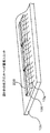
図5は、図4中の光プリントヘッド基板ユニットを示す斜視図である。
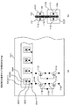
図6(a)、(b)は、図5中のドライバIC100及び発光サイリスタアレイ200からなる半導体複合装置のチップの構成を示す回路図であり、同図(a)は全体の回路図、及び、同図(b)は同図(a)中のシフトレジスタの回路図である。
本発明の実施例1における図6のドライバIC100及び発光サイリスタアレイ200により構成される半導体複合装置からなる複合チップは、例えば、以下の(1)〜(5)の工程により製造される。
図7−1及び図7−2は、図6中のメサ型発光サイリスタ210の製造方法を示す模式的な断面図である。
図7−3は、半導体複合装置の製造方法を示す模式的な断面図である。
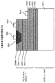
エピフィルム230−1は、n型A1GaAs層232と、n型GaAsコンタクト層233と、InGaPエッチングストップ層234と、p型A1GaAs層235と、n型A1GaAs層236と、InGaPエッチングストップ層237と、p型A1GaAs層238と、p型GaAsコンタクト層239とを順に積層させた構造を持つ。
図7−4(a)、(b)は、複合チップの模式的な平面を示す図であって、後述する配線工程の前の状態が模式的に示されている。このうち、図7−4(a)は複合チップの平面図、及び、図7−4(b)は図7−4(a)中のNチャネルMOSトランジスタ(以下「NMOS」という。)及びPチャネルMOSトランジスタ(以下「PMOS」という。)の平面図である。
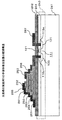
図1は、本発明の実施例1における図7−4の半導体複合装置の配線構造を示す模式的な断面図である。
図8(a)〜(c)は、図7−3及び図1におけるメサ型複合チップの概略の製造工程を示す図であり、同図(a)は処理工程図、同図(b)は概略の断面図、及び同図(c)は概略の平面図である。
図9は、図6の光プリントヘッド13の動作を説明するためのタイムチャートである。
図10は、実施例1の図6(a)における光プリントヘッド13の構成の変形例を示す回路図であり、図6(a)中の要素と共通の要素には共通の符号が付されている。
本実施例1の半導体複合装置とこれを用いた光プリントヘッド13及び画像形成装置1によれば、次のような効果がある。
本発明の実施例2における半導体複合装置からなる複合チップは、例えば、以下の(1)〜(5)の工程により製造される。
図12−1及び図12−2は、拡散型発光サイリスタ210Aの製造方法を示す模式的な断面図であり、実施例1の図7−1及び図7−2中の要素と共通の要素には共通の符号が付されている。
図12−3は、半導体複合装置の製造方法を示す模式的な断面図であり、実施例1の図7−3中の要素と共通の要素には共通の符号が付されている。
エピフィルム230A−1は、n型A1GaAs層232と、n型GaAsコンタクト層233と、InGaPエッチングストップ層234と、p型A1GaAs層235と、n型A1GaAs層236と、n型GaAsコンタクト層239Aとを順に積層させた構造を持つ。
図12−4(a)、(b)は、本実施例2における複合チップの模式的な平面を示す図であって、後述する配線工程の前の状態が模式的に示されている。このうち、図12−4(a)は複合チップの平面図、及び、図12−4(b)は図12−4(a)中のNMOS及びPMOSの平面図である。
図13は、本発明の実施例2における図12−4の半導体複合装置の配線構造を示す模式的な断面図であり、実施例1の図1中の要素と共通の要素には共通の符号が付されている。
図14(a)〜(c)は、図12−3及び図13における拡散型複合チップの概略の製造工程を示す図であり、同図(a)は処理工程図、同図(b)は概略の断面図、及び同図(c)は概略の平面図である。この図14(a)〜(c)は、実施例1の図8(a)〜(c)に対応している。
本実施例2の光プリントヘッド13は、実施例1の図9に示すタイムチャートと同様の動作を行う。
本実施例2の半導体複合装置とこれを用いた光プリントヘッド13及び画像形成装置1によれば、次のような効果がある。
本発明は、上記実施例1、2やこれらの変形例に限定されず、その他の利用形態や変形が可能である。この利用形態や変形例としては、例えば、次の(a)〜(c)のようなものがある。
13 光プリントヘッド
100 ドライバIC
101 シフトレジスタ
200 発光サイリスタアレイ
210,210A,210−1〜210−8 発光サイリスタ
230−1,230A−1 エピフィルム
240 ICウェハ
241 シリコン基板
242 パッシベーション膜
Claims (11)
- 駆動回路を構成する複数の回路構成素子が形成された基板と、
前記基板上に絶縁膜を介して貼着され、前記駆動回路により駆動される複数の被駆動素子が配列された結晶構造を持った半導体薄膜からなる被駆動素子アレイと、
前記複数の回路構成素子間を電気的に接続して前記駆動回路を形成すると共に、前記駆動回路及び前記複数の被駆動素子間を電気的に接続する配線と、
を有することを特徴とする半導体複合装置。 - 駆動回路を構成する複数の回路構成素子が形成された基板と、
前記基板上に絶縁膜を介して貼着され、前記駆動回路により駆動される複数の被駆動素子が配列された結晶構造を持った半導体薄膜からなる被駆動素子アレイと、
前記半導体薄膜中に拡散され、前記被駆動素子の主要部を形成する不純物拡散領域と、
前記複数の回路構成素子間を電気的に接続して前記駆動回路を形成すると共に、前記駆動回路及び前記複数の被駆動素子間を電気的に接続する配線と、
を有することを特徴とする半導体複合装置。 - 前記被駆動素子は、スイッチ素子であることを特徴とする請求項1又は2記載の半導体複合装置。
- 前記スイッチ素子は、電気信号により光を出射する発光素子であることを特徴とする請求項3記載の半導体複合装置。
- 前記発光素子は、PNPN構造又はPNPNPN構造を有する発光サイリスタであることを特徴とする請求項4記載の半導体複合装置。
- 前記駆動回路は、前記複数の被駆動素子を時分割駆動するシフトレジスタであることを特徴とする請求項1〜5のいずれか1項に記載の半導体複合装置。
- 前記複数の回路構成素子は、前記シフトレジスタを構成するためのトランジスタの集合であることを特徴とする請求項6記載の半導体複合装置。
- 駆動回路を構成する複数の回路構成素子が形成された基板を用意する工程と、
前記駆動回路により駆動される複数の被駆動素子が配列された結晶構造を持った半導体薄膜からなる被駆動素子アレイを、パッシベーション膜を介して前記基板上に貼着する工程と、
フォトリソグラフィ法により、前記複数の回路構成素子間を電気的に接続して前記駆動回路を形成すると共に、前記駆動回路及び前記複数の被駆動素子間を電気的に接続するメタル配線を形成する工程と、
を有することを特徴とする半導体複合装置の製造方法。 - 駆動回路を構成する複数の回路構成素子が形成された基板を用意する工程と、
前記駆動回路により駆動される複数の被駆動素子が配列された結晶構造を持った半導体薄膜からなる被駆動素子アレイを、パッシベーション膜を介して前記基板上に貼着する工程と、
前記被駆動素子の主要部を形成する不純物を前記半導体薄膜中に拡散する工程と、
フォトリソグラフィ法により、前記複数の回路構成素子間を電気的に接続して前記駆動回路を形成すると共に、前記駆動回路及び前記複数の被駆動素子間を電気的に接続するメタル配線を形成する工程と、
を有することを特徴とする半導体複合装置の製造方法。 - 請求項4〜7のいずれか1項に記載の半導体複合装置と、
前記複数の発光素子の出射光を収束するレンズアレイと、
を有することを特徴とする光プリントヘッド。 - 請求項10記載の光プリントヘッドを有し、
前記光プリントヘッドにより感光体を露光して静電潜像を形成し、前記静電潜像を現像して記録媒体に画像を形成することを特徴とする画像形成装置。
Priority Applications (2)
| Application Number | Priority Date | Filing Date | Title |
|---|---|---|---|
| JP2009202379A JP2011054760A (ja) | 2009-09-02 | 2009-09-02 | 半導体複合装置、この製造方法、光プリントヘッド及び画像形成装置 |
| US12/873,445 US8704862B2 (en) | 2009-09-02 | 2010-09-01 | Semiconductor composite device, method of manufacturing the same, optical print head and image forming apparatus |
Applications Claiming Priority (1)
| Application Number | Priority Date | Filing Date | Title |
|---|---|---|---|
| JP2009202379A JP2011054760A (ja) | 2009-09-02 | 2009-09-02 | 半導体複合装置、この製造方法、光プリントヘッド及び画像形成装置 |
Publications (2)
| Publication Number | Publication Date |
|---|---|
| JP2011054760A true JP2011054760A (ja) | 2011-03-17 |
| JP2011054760A5 JP2011054760A5 (ja) | 2012-05-17 |
Family
ID=43624280
Family Applications (1)
| Application Number | Title | Priority Date | Filing Date |
|---|---|---|---|
| JP2009202379A Pending JP2011054760A (ja) | 2009-09-02 | 2009-09-02 | 半導体複合装置、この製造方法、光プリントヘッド及び画像形成装置 |
Country Status (2)
| Country | Link |
|---|---|
| US (1) | US8704862B2 (ja) |
| JP (1) | JP2011054760A (ja) |
Cited By (6)
| Publication number | Priority date | Publication date | Assignee | Title |
|---|---|---|---|---|
| JP2014110291A (ja) * | 2012-11-30 | 2014-06-12 | Oki Data Corp | 発光デバイス、発光デバイスの製造方法、発光素子プリントヘッド、及び画像形成装置 |
| JP2015126189A (ja) * | 2013-12-27 | 2015-07-06 | 株式会社沖データ | 半導体装置、半導体装置の製造方法、光プリントヘッド及び画像形成装置 |
| JP2017084992A (ja) * | 2015-10-29 | 2017-05-18 | 株式会社沖データ | 半導体複合装置、光プリントヘッド及び画像形成装置 |
| JP2017135328A (ja) * | 2016-01-29 | 2017-08-03 | 株式会社沖データ | 発光素子装置及び光プリントヘッド |
| JP2019062046A (ja) * | 2017-09-26 | 2019-04-18 | 株式会社沖データ | 発光サイリスタ、光プリントヘッド、及び画像形成装置 |
| JP2019079939A (ja) * | 2017-10-25 | 2019-05-23 | 株式会社沖データ | 半導体装置、光プリントヘッド、及び画像形成装置 |
Families Citing this family (3)
| Publication number | Priority date | Publication date | Assignee | Title |
|---|---|---|---|---|
| JP5366511B2 (ja) * | 2008-11-14 | 2013-12-11 | 株式会社沖データ | 駆動回路、光プリントヘッド及び画像形成装置 |
| US8852994B2 (en) | 2010-05-24 | 2014-10-07 | Masimo Semiconductor, Inc. | Method of fabricating bifacial tandem solar cells |
| US8455290B2 (en) * | 2010-09-04 | 2013-06-04 | Masimo Semiconductor, Inc. | Method of fabricating epitaxial structures |
Citations (5)
| Publication number | Priority date | Publication date | Assignee | Title |
|---|---|---|---|---|
| JPH06123908A (ja) * | 1992-08-31 | 1994-05-06 | Matsushita Electric Ind Co Ltd | 光双安定素子を有するシフトレジスタ |
| JPH09283794A (ja) * | 1996-04-08 | 1997-10-31 | Nippon Sheet Glass Co Ltd | 面発光素子および自己走査型発光装置 |
| JP2001223319A (ja) * | 1999-11-30 | 2001-08-17 | Nissan Motor Co Ltd | 半導体実装構造およびこれに用いる半導体チップセット |
| JP2004128175A (ja) * | 2002-10-02 | 2004-04-22 | Nippon Sheet Glass Co Ltd | 発光素子および自己走査型発光素子アレイチップ |
| JP2004207444A (ja) * | 2002-12-25 | 2004-07-22 | Oki Data Corp | 半導体装置 |
Family Cites Families (1)
| Publication number | Priority date | Publication date | Assignee | Title |
|---|---|---|---|---|
| JP4817774B2 (ja) | 2005-09-14 | 2011-11-16 | 株式会社沖データ | 半導体複合装置光プリントヘッドおよび画像形成装置 |
-
2009
- 2009-09-02 JP JP2009202379A patent/JP2011054760A/ja active Pending
-
2010
- 2010-09-01 US US12/873,445 patent/US8704862B2/en not_active Expired - Fee Related
Patent Citations (5)
| Publication number | Priority date | Publication date | Assignee | Title |
|---|---|---|---|---|
| JPH06123908A (ja) * | 1992-08-31 | 1994-05-06 | Matsushita Electric Ind Co Ltd | 光双安定素子を有するシフトレジスタ |
| JPH09283794A (ja) * | 1996-04-08 | 1997-10-31 | Nippon Sheet Glass Co Ltd | 面発光素子および自己走査型発光装置 |
| JP2001223319A (ja) * | 1999-11-30 | 2001-08-17 | Nissan Motor Co Ltd | 半導体実装構造およびこれに用いる半導体チップセット |
| JP2004128175A (ja) * | 2002-10-02 | 2004-04-22 | Nippon Sheet Glass Co Ltd | 発光素子および自己走査型発光素子アレイチップ |
| JP2004207444A (ja) * | 2002-12-25 | 2004-07-22 | Oki Data Corp | 半導体装置 |
Cited By (6)
| Publication number | Priority date | Publication date | Assignee | Title |
|---|---|---|---|---|
| JP2014110291A (ja) * | 2012-11-30 | 2014-06-12 | Oki Data Corp | 発光デバイス、発光デバイスの製造方法、発光素子プリントヘッド、及び画像形成装置 |
| JP2015126189A (ja) * | 2013-12-27 | 2015-07-06 | 株式会社沖データ | 半導体装置、半導体装置の製造方法、光プリントヘッド及び画像形成装置 |
| JP2017084992A (ja) * | 2015-10-29 | 2017-05-18 | 株式会社沖データ | 半導体複合装置、光プリントヘッド及び画像形成装置 |
| JP2017135328A (ja) * | 2016-01-29 | 2017-08-03 | 株式会社沖データ | 発光素子装置及び光プリントヘッド |
| JP2019062046A (ja) * | 2017-09-26 | 2019-04-18 | 株式会社沖データ | 発光サイリスタ、光プリントヘッド、及び画像形成装置 |
| JP2019079939A (ja) * | 2017-10-25 | 2019-05-23 | 株式会社沖データ | 半導体装置、光プリントヘッド、及び画像形成装置 |
Also Published As
| Publication number | Publication date |
|---|---|
| US20110050838A1 (en) | 2011-03-03 |
| US8704862B2 (en) | 2014-04-22 |
Similar Documents
| Publication | Publication Date | Title |
|---|---|---|
| JP2011054760A (ja) | 半導体複合装置、この製造方法、光プリントヘッド及び画像形成装置 | |
| JP4817774B2 (ja) | 半導体複合装置光プリントヘッドおよび画像形成装置 | |
| US8035115B2 (en) | Semiconductor apparatus, print head, and image forming apparatus | |
| US8343848B2 (en) | Semiconductor device, LED print head and image-forming apparatus using same, and method of manufacturing semiconductor device | |
| US8542262B2 (en) | Light emitting element array, drive circuit, optical print head, and image forming apparatus | |
| US8497893B2 (en) | Semiconductor device, optical print head and image forming apparatus | |
| JP2006253370A (ja) | 半導体装置、プリントヘッド、及びそれを用いた画像形成装置 | |
| US8581946B2 (en) | Driving device, optical print head and image forming device | |
| JP4672329B2 (ja) | 半導体装置、及び、それを用いたledプリントヘッド、画像形成装置、半導体装置の製造方法 | |
| JP2009289836A (ja) | 発光素子アレイ、駆動制御装置、記録ヘッドおよび画像形成装置 | |
| US8471884B2 (en) | Driving device, print head and image forming device | |
| JP4731949B2 (ja) | 半導体装置、ledヘッド、及びこれを用いた画像形成装置 | |
| JP2011194810A (ja) | 駆動装置、プリントヘッド及び画像形成装置 | |
| JP2005079262A (ja) | 半導体装置、ledヘッド、及び画像形成装置 | |
| US8836743B2 (en) | Drive device, print head and image forming apparatus | |
| JP2015126189A (ja) | 半導体装置、半導体装置の製造方法、光プリントヘッド及び画像形成装置 | |
| JP2005167062A (ja) | 半導体装置、ledヘッド、及びプリンタ | |
| JP5197318B2 (ja) | 駆動回路、記録ヘッド、画像形成装置および表示装置 | |
| JP5460350B2 (ja) | 駆動回路、駆動装置及び画像形成装置 | |
| US8614728B2 (en) | Driver device, print head, and image formation apparatus | |
| US8587628B2 (en) | Driver apparatus, print head, and image forming apparatus | |
| JP6129777B2 (ja) | 半導体装置、半導体装置の製造方法、プリントヘッド、及び画像形成装置 |
Legal Events
| Date | Code | Title | Description |
|---|---|---|---|
| A521 | Request for written amendment filed |
Free format text: JAPANESE INTERMEDIATE CODE: A523 Effective date: 20120322 |
|
| A621 | Written request for application examination |
Free format text: JAPANESE INTERMEDIATE CODE: A621 Effective date: 20120322 |
|
| A131 | Notification of reasons for refusal |
Free format text: JAPANESE INTERMEDIATE CODE: A131 Effective date: 20131203 |
|
| A521 | Request for written amendment filed |
Free format text: JAPANESE INTERMEDIATE CODE: A523 Effective date: 20140115 |
|
| A131 | Notification of reasons for refusal |
Free format text: JAPANESE INTERMEDIATE CODE: A131 Effective date: 20140603 |
|
| A02 | Decision of refusal |
Free format text: JAPANESE INTERMEDIATE CODE: A02 Effective date: 20141111 |