JP2010537444A - エッチング剤組成物及び金属Cu/Moのためのエッチング方法 - Google Patents
エッチング剤組成物及び金属Cu/Moのためのエッチング方法 Download PDFInfo
- Publication number
- JP2010537444A JP2010537444A JP2010522406A JP2010522406A JP2010537444A JP 2010537444 A JP2010537444 A JP 2010537444A JP 2010522406 A JP2010522406 A JP 2010522406A JP 2010522406 A JP2010522406 A JP 2010522406A JP 2010537444 A JP2010537444 A JP 2010537444A
- Authority
- JP
- Japan
- Prior art keywords
- layer
- etching
- acid
- weight
- composition
- Prior art date
- Legal status (The legal status is an assumption and is not a legal conclusion. Google has not performed a legal analysis and makes no representation as to the accuracy of the status listed.)
- Pending
Links
- 239000000203 mixture Substances 0.000 title claims abstract description 79
- 238000005530 etching Methods 0.000 title claims abstract description 51
- 238000000034 method Methods 0.000 title claims abstract description 19
- 229910052751 metal Inorganic materials 0.000 title claims abstract description 14
- 239000002184 metal Substances 0.000 title claims abstract description 14
- MHAJPDPJQMAIIY-UHFFFAOYSA-N Hydrogen peroxide Chemical compound OO MHAJPDPJQMAIIY-UHFFFAOYSA-N 0.000 claims abstract description 16
- 230000002378 acidificating effect Effects 0.000 claims abstract description 11
- 150000001413 amino acids Chemical class 0.000 claims abstract description 11
- 239000003381 stabilizer Substances 0.000 claims abstract description 11
- 239000003002 pH adjusting agent Substances 0.000 claims abstract description 9
- 239000012736 aqueous medium Substances 0.000 claims abstract description 7
- 239000000758 substrate Substances 0.000 claims description 21
- 239000002253 acid Substances 0.000 claims description 12
- 239000003795 chemical substances by application Substances 0.000 claims description 12
- KRHYYFGTRYWZRS-UHFFFAOYSA-N Fluorane Chemical compound F KRHYYFGTRYWZRS-UHFFFAOYSA-N 0.000 claims description 10
- YCKRFDGAMUMZLT-UHFFFAOYSA-N Fluorine atom Chemical compound [F] YCKRFDGAMUMZLT-UHFFFAOYSA-N 0.000 claims description 10
- 235000001014 amino acid Nutrition 0.000 claims description 10
- 239000011737 fluorine Substances 0.000 claims description 10
- 229910052731 fluorine Inorganic materials 0.000 claims description 10
- 229910052802 copper Inorganic materials 0.000 claims description 9
- NBIIXXVUZAFLBC-UHFFFAOYSA-N Phosphoric acid Chemical group OP(O)(O)=O NBIIXXVUZAFLBC-UHFFFAOYSA-N 0.000 claims description 8
- DHMQDGOQFOQNFH-UHFFFAOYSA-N Glycine Chemical compound NCC(O)=O DHMQDGOQFOQNFH-UHFFFAOYSA-N 0.000 claims description 7
- 229920002120 photoresistant polymer Polymers 0.000 claims description 7
- QTBSBXVTEAMEQO-UHFFFAOYSA-N Acetic acid Chemical compound CC(O)=O QTBSBXVTEAMEQO-UHFFFAOYSA-N 0.000 claims description 6
- MUBZPKHOEPUJKR-UHFFFAOYSA-N Oxalic acid Chemical compound OC(=O)C(O)=O MUBZPKHOEPUJKR-UHFFFAOYSA-N 0.000 claims description 6
- KRKNYBCHXYNGOX-UHFFFAOYSA-N citric acid Chemical compound OC(=O)CC(O)(C(O)=O)CC(O)=O KRKNYBCHXYNGOX-UHFFFAOYSA-N 0.000 claims description 6
- 229910052750 molybdenum Inorganic materials 0.000 claims description 6
- 238000005240 physical vapour deposition Methods 0.000 claims description 5
- DDFHBQSCUXNBSA-UHFFFAOYSA-N 5-(5-carboxythiophen-2-yl)thiophene-2-carboxylic acid Chemical group S1C(C(=O)O)=CC=C1C1=CC=C(C(O)=O)S1 DDFHBQSCUXNBSA-UHFFFAOYSA-N 0.000 claims description 4
- 229910000147 aluminium phosphate Inorganic materials 0.000 claims description 4
- 238000005229 chemical vapour deposition Methods 0.000 claims description 4
- XLYOFNOQVPJJNP-UHFFFAOYSA-N water Chemical group O XLYOFNOQVPJJNP-UHFFFAOYSA-N 0.000 claims description 4
- 239000004254 Ammonium phosphate Substances 0.000 claims description 3
- -1 EDTA salt Chemical class 0.000 claims description 3
- 239000004471 Glycine Substances 0.000 claims description 3
- QNAYBMKLOCPYGJ-REOHCLBHSA-N L-alanine Chemical compound C[C@H](N)C(O)=O QNAYBMKLOCPYGJ-REOHCLBHSA-N 0.000 claims description 3
- 235000004279 alanine Nutrition 0.000 claims description 3
- 229910000148 ammonium phosphate Inorganic materials 0.000 claims description 3
- 235000019289 ammonium phosphates Nutrition 0.000 claims description 3
- 239000008367 deionised water Substances 0.000 claims description 3
- 229910021641 deionized water Inorganic materials 0.000 claims description 3
- MNNHAPBLZZVQHP-UHFFFAOYSA-N diammonium hydrogen phosphate Chemical compound [NH4+].[NH4+].OP([O-])([O-])=O MNNHAPBLZZVQHP-UHFFFAOYSA-N 0.000 claims description 3
- 229910000881 Cu alloy Inorganic materials 0.000 claims description 2
- KCXVZYZYPLLWCC-UHFFFAOYSA-N EDTA Chemical compound OC(=O)CN(CC(O)=O)CCN(CC(O)=O)CC(O)=O KCXVZYZYPLLWCC-UHFFFAOYSA-N 0.000 claims description 2
- 229910001182 Mo alloy Inorganic materials 0.000 claims description 2
- 229910017855 NH 4 F Inorganic materials 0.000 claims description 2
- KVBCYCWRDBDGBG-UHFFFAOYSA-N azane;dihydrofluoride Chemical compound [NH4+].F.[F-] KVBCYCWRDBDGBG-UHFFFAOYSA-N 0.000 claims description 2
- 238000007772 electroless plating Methods 0.000 claims description 2
- 238000009713 electroplating Methods 0.000 claims description 2
- 125000000896 monocarboxylic acid group Chemical group 0.000 claims description 2
- QPJSUIGXIBEQAC-UHFFFAOYSA-N n-(2,4-dichloro-5-propan-2-yloxyphenyl)acetamide Chemical compound CC(C)OC1=CC(NC(C)=O)=C(Cl)C=C1Cl QPJSUIGXIBEQAC-UHFFFAOYSA-N 0.000 claims description 2
- 235000006408 oxalic acid Nutrition 0.000 claims description 2
- 239000010949 copper Substances 0.000 description 41
- RYGMFSIKBFXOCR-UHFFFAOYSA-N Copper Chemical compound [Cu] RYGMFSIKBFXOCR-UHFFFAOYSA-N 0.000 description 8
- 239000011521 glass Substances 0.000 description 6
- 150000007513 acids Chemical class 0.000 description 3
- XUIMIQQOPSSXEZ-UHFFFAOYSA-N Silicon Chemical compound [Si] XUIMIQQOPSSXEZ-UHFFFAOYSA-N 0.000 description 2
- 238000004519 manufacturing process Methods 0.000 description 2
- 238000012986 modification Methods 0.000 description 2
- 230000004048 modification Effects 0.000 description 2
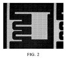
- 238000000879 optical micrograph Methods 0.000 description 2
- 239000010703 silicon Substances 0.000 description 2
- 229910052710 silicon Inorganic materials 0.000 description 2
- 239000004593 Epoxy Substances 0.000 description 1
- ZOKXTWBITQBERF-UHFFFAOYSA-N Molybdenum Chemical compound [Mo] ZOKXTWBITQBERF-UHFFFAOYSA-N 0.000 description 1
- 239000004642 Polyimide Substances 0.000 description 1
- 230000002411 adverse Effects 0.000 description 1
- 229910052782 aluminium Inorganic materials 0.000 description 1
- XAGFODPZIPBFFR-UHFFFAOYSA-N aluminium Chemical compound [Al] XAGFODPZIPBFFR-UHFFFAOYSA-N 0.000 description 1
- 230000005540 biological transmission Effects 0.000 description 1
- 239000011889 copper foil Substances 0.000 description 1
- 238000011161 development Methods 0.000 description 1
- 239000007769 metal material Substances 0.000 description 1
- 239000011733 molybdenum Substances 0.000 description 1
- 230000001590 oxidative effect Effects 0.000 description 1
- 229920001721 polyimide Polymers 0.000 description 1
- 230000001681 protective effect Effects 0.000 description 1
- 238000011160 research Methods 0.000 description 1
- 230000027756 respiratory electron transport chain Effects 0.000 description 1
- 239000004065 semiconductor Substances 0.000 description 1
Images


Classifications
-
- C—CHEMISTRY; METALLURGY
- C09—DYES; PAINTS; POLISHES; NATURAL RESINS; ADHESIVES; COMPOSITIONS NOT OTHERWISE PROVIDED FOR; APPLICATIONS OF MATERIALS NOT OTHERWISE PROVIDED FOR
- C09K—MATERIALS FOR MISCELLANEOUS APPLICATIONS, NOT PROVIDED FOR ELSEWHERE
- C09K13/00—Etching, surface-brightening or pickling compositions
- C09K13/04—Etching, surface-brightening or pickling compositions containing an inorganic acid
- C09K13/08—Etching, surface-brightening or pickling compositions containing an inorganic acid containing a fluorine compound
-
- C—CHEMISTRY; METALLURGY
- C23—COATING METALLIC MATERIAL; COATING MATERIAL WITH METALLIC MATERIAL; CHEMICAL SURFACE TREATMENT; DIFFUSION TREATMENT OF METALLIC MATERIAL; COATING BY VACUUM EVAPORATION, BY SPUTTERING, BY ION IMPLANTATION OR BY CHEMICAL VAPOUR DEPOSITION, IN GENERAL; INHIBITING CORROSION OF METALLIC MATERIAL OR INCRUSTATION IN GENERAL
- C23F—NON-MECHANICAL REMOVAL OF METALLIC MATERIAL FROM SURFACE; INHIBITING CORROSION OF METALLIC MATERIAL OR INCRUSTATION IN GENERAL; MULTI-STEP PROCESSES FOR SURFACE TREATMENT OF METALLIC MATERIAL INVOLVING AT LEAST ONE PROCESS PROVIDED FOR IN CLASS C23 AND AT LEAST ONE PROCESS COVERED BY SUBCLASS C21D OR C22F OR CLASS C25
- C23F1/00—Etching metallic material by chemical means
- C23F1/10—Etching compositions
- C23F1/14—Aqueous compositions
- C23F1/16—Acidic compositions
- C23F1/18—Acidic compositions for etching copper or alloys thereof
-
- C—CHEMISTRY; METALLURGY
- C23—COATING METALLIC MATERIAL; COATING MATERIAL WITH METALLIC MATERIAL; CHEMICAL SURFACE TREATMENT; DIFFUSION TREATMENT OF METALLIC MATERIAL; COATING BY VACUUM EVAPORATION, BY SPUTTERING, BY ION IMPLANTATION OR BY CHEMICAL VAPOUR DEPOSITION, IN GENERAL; INHIBITING CORROSION OF METALLIC MATERIAL OR INCRUSTATION IN GENERAL
- C23F—NON-MECHANICAL REMOVAL OF METALLIC MATERIAL FROM SURFACE; INHIBITING CORROSION OF METALLIC MATERIAL OR INCRUSTATION IN GENERAL; MULTI-STEP PROCESSES FOR SURFACE TREATMENT OF METALLIC MATERIAL INVOLVING AT LEAST ONE PROCESS PROVIDED FOR IN CLASS C23 AND AT LEAST ONE PROCESS COVERED BY SUBCLASS C21D OR C22F OR CLASS C25
- C23F1/00—Etching metallic material by chemical means
- C23F1/10—Etching compositions
- C23F1/14—Aqueous compositions
- C23F1/16—Acidic compositions
- C23F1/26—Acidic compositions for etching refractory metals
-
- H—ELECTRICITY
- H01—ELECTRIC ELEMENTS
- H01L—SEMICONDUCTOR DEVICES NOT COVERED BY CLASS H10
- H01L21/00—Processes or apparatus adapted for the manufacture or treatment of semiconductor or solid state devices or of parts thereof
- H01L21/02—Manufacture or treatment of semiconductor devices or of parts thereof
- H01L21/04—Manufacture or treatment of semiconductor devices or of parts thereof the devices having potential barriers, e.g. a PN junction, depletion layer or carrier concentration layer
- H01L21/18—Manufacture or treatment of semiconductor devices or of parts thereof the devices having potential barriers, e.g. a PN junction, depletion layer or carrier concentration layer the devices having semiconductor bodies comprising elements of Group IV of the Periodic Table or AIIIBV compounds with or without impurities, e.g. doping materials
- H01L21/30—Treatment of semiconductor bodies using processes or apparatus not provided for in groups H01L21/20 - H01L21/26
- H01L21/31—Treatment of semiconductor bodies using processes or apparatus not provided for in groups H01L21/20 - H01L21/26 to form insulating layers thereon, e.g. for masking or by using photolithographic techniques; After treatment of these layers; Selection of materials for these layers
- H01L21/3205—Deposition of non-insulating-, e.g. conductive- or resistive-, layers on insulating layers; After-treatment of these layers
- H01L21/321—After treatment
- H01L21/3213—Physical or chemical etching of the layers, e.g. to produce a patterned layer from a pre-deposited extensive layer
- H01L21/32133—Physical or chemical etching of the layers, e.g. to produce a patterned layer from a pre-deposited extensive layer by chemical means only
- H01L21/32134—Physical or chemical etching of the layers, e.g. to produce a patterned layer from a pre-deposited extensive layer by chemical means only by liquid etching only
Landscapes
- Chemical & Material Sciences (AREA)
- Engineering & Computer Science (AREA)
- Materials Engineering (AREA)
- Organic Chemistry (AREA)
- Chemical Kinetics & Catalysis (AREA)
- General Chemical & Material Sciences (AREA)
- Metallurgy (AREA)
- Mechanical Engineering (AREA)
- Condensed Matter Physics & Semiconductors (AREA)
- General Physics & Mathematics (AREA)
- Manufacturing & Machinery (AREA)
- Computer Hardware Design (AREA)
- Microelectronics & Electronic Packaging (AREA)
- Power Engineering (AREA)
- Physics & Mathematics (AREA)
- Inorganic Chemistry (AREA)
- Weting (AREA)
- ing And Chemical Polishing (AREA)
Applications Claiming Priority (3)
| Application Number | Priority Date | Filing Date | Title |
|---|---|---|---|
| TW96137710A TW200916605A (en) | 2007-10-08 | 2007-10-08 | Etchant compositions and etching method for metals Cu/Mo |
| CNA2007101673174A CN101418449A (zh) | 2007-10-22 | 2007-10-22 | 用于铜/钼金属的蚀刻液组成物及蚀刻方法 |
| PCT/EP2008/063221 WO2009047203A1 (en) | 2007-10-08 | 2008-10-02 | ETCHANT COMPOSITIONS AND ETCHING METHOD FOR METALS Cu/Mo |
Publications (2)
| Publication Number | Publication Date |
|---|---|
| JP2010537444A true JP2010537444A (ja) | 2010-12-02 |
| JP2010537444A5 JP2010537444A5 (enExample) | 2012-02-02 |
Family
ID=40219299
Family Applications (1)
| Application Number | Title | Priority Date | Filing Date |
|---|---|---|---|
| JP2010522406A Pending JP2010537444A (ja) | 2007-10-08 | 2008-10-02 | エッチング剤組成物及び金属Cu/Moのためのエッチング方法 |
Country Status (4)
| Country | Link |
|---|---|
| US (1) | US20100301010A1 (enExample) |
| JP (1) | JP2010537444A (enExample) |
| KR (1) | KR20100064361A (enExample) |
| WO (1) | WO2009047203A1 (enExample) |
Cited By (1)
| Publication number | Priority date | Publication date | Assignee | Title |
|---|---|---|---|---|
| JP2013060634A (ja) * | 2011-09-14 | 2013-04-04 | Tosoh Corp | エッチング液 |
Families Citing this family (12)
| Publication number | Priority date | Publication date | Assignee | Title |
|---|---|---|---|---|
| KR101153510B1 (ko) * | 2009-02-16 | 2012-06-11 | 히다치 가세고교 가부시끼가이샤 | 구리 연마용 연마제 및 이를 이용한 연마 방법 |
| JP5516426B2 (ja) | 2009-02-16 | 2014-06-11 | 日立化成株式会社 | 研磨剤及び研磨方法 |
| US20120319033A1 (en) * | 2010-02-15 | 2012-12-20 | Mitsubishi Gas Chemical Company, Inc. | Etching solution for multilayer thin film having copper layer and molybdenum layer contained therein |
| KR20120066950A (ko) | 2010-12-15 | 2012-06-25 | 삼성전자주식회사 | 식각액, 이를 이용한 표시 장치 및 그 제조 방법 |
| KR20140013310A (ko) | 2012-07-23 | 2014-02-05 | 삼성디스플레이 주식회사 | 식각액 조성물, 및 이를 이용한 금속 배선과 박막 트랜지스터 표시판 제조 방법 |
| KR20150124540A (ko) | 2014-04-28 | 2015-11-06 | 삼성디스플레이 주식회사 | 식각액 및 이를 이용한 표시 장치의 제조 방법 |
| KR102218353B1 (ko) * | 2014-06-26 | 2021-02-22 | 동우 화인켐 주식회사 | 금속막의 식각액 조성물 및 이를 이용한 액정표시장치용 어레이 기판의 제조방법 |
| KR102209680B1 (ko) * | 2014-06-27 | 2021-01-29 | 동우 화인켐 주식회사 | 금속막의 식각액 조성물 및 이를 이용한 액정 표시 장치용 어레이 기판의 제조방법 |
| TWI618817B (zh) * | 2015-12-29 | 2018-03-21 | Daxin Materials Corporation | 蝕刻液組成物及應用其之蝕刻方法 |
| WO2019054294A1 (ja) * | 2017-09-12 | 2019-03-21 | 株式会社 東芝 | セラミックス回路基板の製造方法 |
| TWI789741B (zh) * | 2020-04-14 | 2023-01-11 | 美商恩特葛瑞斯股份有限公司 | 蝕刻鉬之方法及組合物 |
| KR102889639B1 (ko) * | 2020-07-01 | 2025-11-21 | 삼성디스플레이 주식회사 | 표시 장치 및 그 제조 방법 |
Citations (4)
| Publication number | Priority date | Publication date | Assignee | Title |
|---|---|---|---|---|
| JP2004193620A (ja) * | 2002-12-12 | 2004-07-08 | Lg Phillips Lcd Co Ltd | 銅モリブデン膜で、モリブデンの残渣を除去するエッチング溶液及びそのエッチング方法 |
| WO2006138235A2 (en) * | 2005-06-13 | 2006-12-28 | Advanced Technology Materials, Inc. | Compositions and methods for selective removal of metal or metal alloy after metal silicide formation |
| JP2007005790A (ja) * | 2005-06-22 | 2007-01-11 | Samsung Electronics Co Ltd | エッチング液、これを用いた配線形成方法及び薄膜トランジスタ基板の製造方法 |
| WO2008121952A1 (en) * | 2007-03-31 | 2008-10-09 | Advanced Technology Materials, Inc. | Methods for stripping material for wafer reclamation |
Family Cites Families (3)
| Publication number | Priority date | Publication date | Assignee | Title |
|---|---|---|---|---|
| KR101190907B1 (ko) * | 2004-12-07 | 2012-10-12 | 가오 가부시키가이샤 | 박리제 조성물 |
| TWI378989B (en) * | 2006-09-01 | 2012-12-11 | Taiwan Tft Lcd Ass | Etchant for patterning composite layer and method of fabricating thin film transistor using the same |
| KR101326128B1 (ko) * | 2006-09-29 | 2013-11-06 | 삼성디스플레이 주식회사 | 표시 장치용 배선, 식각액, 박막 트랜지스터 표시판 및 그제조 방법 |
-
2008
- 2008-10-02 US US12/675,131 patent/US20100301010A1/en not_active Abandoned
- 2008-10-02 KR KR1020107004302A patent/KR20100064361A/ko not_active Withdrawn
- 2008-10-02 WO PCT/EP2008/063221 patent/WO2009047203A1/en not_active Ceased
- 2008-10-02 JP JP2010522406A patent/JP2010537444A/ja active Pending
Patent Citations (4)
| Publication number | Priority date | Publication date | Assignee | Title |
|---|---|---|---|---|
| JP2004193620A (ja) * | 2002-12-12 | 2004-07-08 | Lg Phillips Lcd Co Ltd | 銅モリブデン膜で、モリブデンの残渣を除去するエッチング溶液及びそのエッチング方法 |
| WO2006138235A2 (en) * | 2005-06-13 | 2006-12-28 | Advanced Technology Materials, Inc. | Compositions and methods for selective removal of metal or metal alloy after metal silicide formation |
| JP2007005790A (ja) * | 2005-06-22 | 2007-01-11 | Samsung Electronics Co Ltd | エッチング液、これを用いた配線形成方法及び薄膜トランジスタ基板の製造方法 |
| WO2008121952A1 (en) * | 2007-03-31 | 2008-10-09 | Advanced Technology Materials, Inc. | Methods for stripping material for wafer reclamation |
Cited By (1)
| Publication number | Priority date | Publication date | Assignee | Title |
|---|---|---|---|---|
| JP2013060634A (ja) * | 2011-09-14 | 2013-04-04 | Tosoh Corp | エッチング液 |
Also Published As
| Publication number | Publication date |
|---|---|
| KR20100064361A (ko) | 2010-06-14 |
| US20100301010A1 (en) | 2010-12-02 |
| WO2009047203A1 (en) | 2009-04-16 |
Similar Documents
| Publication | Publication Date | Title |
|---|---|---|
| JP2010537444A (ja) | エッチング剤組成物及び金属Cu/Moのためのエッチング方法 | |
| JP5913869B2 (ja) | エッチング液組成物およびエッチング方法 | |
| JP2010537444A5 (enExample) | ||
| TWI816635B (zh) | 半導體元件之洗淨用液體組成物、半導體元件之洗淨方法及半導體元件之製造方法 | |
| JPH09181028A (ja) | 半導体素子の洗浄液 | |
| TWI460311B (zh) | 用於撓性配線基板之鎳-鉻合金剝離劑 | |
| CN106952803A (zh) | 半导体元件的清洗用液体组合物及半导体元件的清洗方法、以及半导体元件的制造方法 | |
| CN101418449A (zh) | 用于铜/钼金属的蚀刻液组成物及蚀刻方法 | |
| JP4428995B2 (ja) | 金属膜のエッチング液組成物 | |
| KR20200098108A (ko) | 구리 또는 구리 함유 금속막 식각액 조성물 | |
| JP2004325918A (ja) | 剥離剤組成物 | |
| JP2007005656A (ja) | メタル材料用エッチング剤組成物及びそれを用いた半導体デバイスの製造方法 | |
| JP2008216843A (ja) | フォトレジスト剥離液組成物 | |
| CN100549840C (zh) | 剥离剂组合物 | |
| JP6378271B2 (ja) | タングステン膜エッチング液組成物、これを用いた電子デバイスの製造方法および電子デバイス | |
| JP7650265B2 (ja) | チタンおよび/またはチタン合金のエッチング液、該エッチング液を用いたチタンおよび/またはチタン合金のエッチング方法、および該エッチング液を用いた基板の製造方法 | |
| JP2013060634A (ja) | エッチング液 | |
| WO2019186624A1 (ja) | エッチング液 | |
| JP4632038B2 (ja) | 銅配線基板製造方法 | |
| TWI759450B (zh) | 蝕刻液、蝕刻方法、及顯示裝置之製造方法 | |
| KR20210032052A (ko) | 구리계 금속막 식각용 조성물 및 이를 이용한 식각방법 | |
| JP4577095B2 (ja) | 金属チタンのエッチング用組成物及びそれを用いたエッチング方法 | |
| TWI660030B (zh) | 含銅金屬用之蝕刻劑組成物 | |
| JP2010150609A (ja) | エッチング液及びエッチング方法 | |
| JPH02265932A (ja) | 有機重合体材料のエッチング方法 |
Legal Events
| Date | Code | Title | Description |
|---|---|---|---|
| RD04 | Notification of resignation of power of attorney |
Free format text: JAPANESE INTERMEDIATE CODE: A7424 Effective date: 20101228 |
|
| A521 | Request for written amendment filed |
Free format text: JAPANESE INTERMEDIATE CODE: A523 Effective date: 20111206 |
|
| A977 | Report on retrieval |
Free format text: JAPANESE INTERMEDIATE CODE: A971007 Effective date: 20120130 |
|
| A131 | Notification of reasons for refusal |
Free format text: JAPANESE INTERMEDIATE CODE: A131 Effective date: 20120203 |
|
| A02 | Decision of refusal |
Free format text: JAPANESE INTERMEDIATE CODE: A02 Effective date: 20120628 |