JP2010537444A - Etching composition and etching method for metal Cu / Mo - Google Patents
Etching composition and etching method for metal Cu / Mo Download PDFInfo
- Publication number
- JP2010537444A JP2010537444A JP2010522406A JP2010522406A JP2010537444A JP 2010537444 A JP2010537444 A JP 2010537444A JP 2010522406 A JP2010522406 A JP 2010522406A JP 2010522406 A JP2010522406 A JP 2010522406A JP 2010537444 A JP2010537444 A JP 2010537444A
- Authority
- JP
- Japan
- Prior art keywords
- layer
- etching
- acid
- weight
- composition
- Prior art date
- Legal status (The legal status is an assumption and is not a legal conclusion. Google has not performed a legal analysis and makes no representation as to the accuracy of the status listed.)
- Pending
Links
- 239000000203 mixture Substances 0.000 title claims abstract description 79
- 238000005530 etching Methods 0.000 title claims abstract description 51
- 238000000034 method Methods 0.000 title claims abstract description 19
- 229910052751 metal Inorganic materials 0.000 title claims abstract description 14
- 239000002184 metal Substances 0.000 title claims abstract description 14
- MHAJPDPJQMAIIY-UHFFFAOYSA-N Hydrogen peroxide Chemical compound OO MHAJPDPJQMAIIY-UHFFFAOYSA-N 0.000 claims abstract description 16
- 230000002378 acidificating effect Effects 0.000 claims abstract description 11
- 150000001413 amino acids Chemical class 0.000 claims abstract description 11
- 239000003381 stabilizer Substances 0.000 claims abstract description 11
- 239000003002 pH adjusting agent Substances 0.000 claims abstract description 9
- 239000012736 aqueous medium Substances 0.000 claims abstract description 7
- 239000000758 substrate Substances 0.000 claims description 21
- 239000002253 acid Substances 0.000 claims description 12
- 239000003795 chemical substances by application Substances 0.000 claims description 12
- KRHYYFGTRYWZRS-UHFFFAOYSA-N Fluorane Chemical compound F KRHYYFGTRYWZRS-UHFFFAOYSA-N 0.000 claims description 10
- YCKRFDGAMUMZLT-UHFFFAOYSA-N Fluorine atom Chemical compound [F] YCKRFDGAMUMZLT-UHFFFAOYSA-N 0.000 claims description 10
- 235000001014 amino acid Nutrition 0.000 claims description 10
- 239000011737 fluorine Substances 0.000 claims description 10
- 229910052731 fluorine Inorganic materials 0.000 claims description 10
- 229910052802 copper Inorganic materials 0.000 claims description 9
- NBIIXXVUZAFLBC-UHFFFAOYSA-N Phosphoric acid Chemical group OP(O)(O)=O NBIIXXVUZAFLBC-UHFFFAOYSA-N 0.000 claims description 8
- DHMQDGOQFOQNFH-UHFFFAOYSA-N Glycine Chemical compound NCC(O)=O DHMQDGOQFOQNFH-UHFFFAOYSA-N 0.000 claims description 7
- 229920002120 photoresistant polymer Polymers 0.000 claims description 7
- QTBSBXVTEAMEQO-UHFFFAOYSA-N Acetic acid Chemical compound CC(O)=O QTBSBXVTEAMEQO-UHFFFAOYSA-N 0.000 claims description 6
- MUBZPKHOEPUJKR-UHFFFAOYSA-N Oxalic acid Chemical compound OC(=O)C(O)=O MUBZPKHOEPUJKR-UHFFFAOYSA-N 0.000 claims description 6
- KRKNYBCHXYNGOX-UHFFFAOYSA-N citric acid Chemical compound OC(=O)CC(O)(C(O)=O)CC(O)=O KRKNYBCHXYNGOX-UHFFFAOYSA-N 0.000 claims description 6
- 229910052750 molybdenum Inorganic materials 0.000 claims description 6
- 238000005240 physical vapour deposition Methods 0.000 claims description 5
- DDFHBQSCUXNBSA-UHFFFAOYSA-N 5-(5-carboxythiophen-2-yl)thiophene-2-carboxylic acid Chemical group S1C(C(=O)O)=CC=C1C1=CC=C(C(O)=O)S1 DDFHBQSCUXNBSA-UHFFFAOYSA-N 0.000 claims description 4
- 229910000147 aluminium phosphate Inorganic materials 0.000 claims description 4
- 238000005229 chemical vapour deposition Methods 0.000 claims description 4
- XLYOFNOQVPJJNP-UHFFFAOYSA-N water Chemical group O XLYOFNOQVPJJNP-UHFFFAOYSA-N 0.000 claims description 4
- 239000004254 Ammonium phosphate Substances 0.000 claims description 3
- -1 EDTA salt Chemical class 0.000 claims description 3
- 239000004471 Glycine Substances 0.000 claims description 3
- QNAYBMKLOCPYGJ-REOHCLBHSA-N L-alanine Chemical compound C[C@H](N)C(O)=O QNAYBMKLOCPYGJ-REOHCLBHSA-N 0.000 claims description 3
- 235000004279 alanine Nutrition 0.000 claims description 3
- 229910000148 ammonium phosphate Inorganic materials 0.000 claims description 3
- 235000019289 ammonium phosphates Nutrition 0.000 claims description 3
- 239000008367 deionised water Substances 0.000 claims description 3
- 229910021641 deionized water Inorganic materials 0.000 claims description 3
- MNNHAPBLZZVQHP-UHFFFAOYSA-N diammonium hydrogen phosphate Chemical compound [NH4+].[NH4+].OP([O-])([O-])=O MNNHAPBLZZVQHP-UHFFFAOYSA-N 0.000 claims description 3
- 229910000881 Cu alloy Inorganic materials 0.000 claims description 2
- KCXVZYZYPLLWCC-UHFFFAOYSA-N EDTA Chemical compound OC(=O)CN(CC(O)=O)CCN(CC(O)=O)CC(O)=O KCXVZYZYPLLWCC-UHFFFAOYSA-N 0.000 claims description 2
- 229910001182 Mo alloy Inorganic materials 0.000 claims description 2
- 229910017855 NH 4 F Inorganic materials 0.000 claims description 2
- KVBCYCWRDBDGBG-UHFFFAOYSA-N azane;dihydrofluoride Chemical compound [NH4+].F.[F-] KVBCYCWRDBDGBG-UHFFFAOYSA-N 0.000 claims description 2
- 238000007772 electroless plating Methods 0.000 claims description 2
- 238000009713 electroplating Methods 0.000 claims description 2
- 125000000896 monocarboxylic acid group Chemical group 0.000 claims description 2
- QPJSUIGXIBEQAC-UHFFFAOYSA-N n-(2,4-dichloro-5-propan-2-yloxyphenyl)acetamide Chemical compound CC(C)OC1=CC(NC(C)=O)=C(Cl)C=C1Cl QPJSUIGXIBEQAC-UHFFFAOYSA-N 0.000 claims description 2
- 235000006408 oxalic acid Nutrition 0.000 claims description 2
- 239000010949 copper Substances 0.000 description 41
- RYGMFSIKBFXOCR-UHFFFAOYSA-N Copper Chemical compound [Cu] RYGMFSIKBFXOCR-UHFFFAOYSA-N 0.000 description 8
- 239000011521 glass Substances 0.000 description 6
- 150000007513 acids Chemical class 0.000 description 3
- XUIMIQQOPSSXEZ-UHFFFAOYSA-N Silicon Chemical compound [Si] XUIMIQQOPSSXEZ-UHFFFAOYSA-N 0.000 description 2
- 238000004519 manufacturing process Methods 0.000 description 2
- 238000012986 modification Methods 0.000 description 2
- 230000004048 modification Effects 0.000 description 2
- 238000000879 optical micrograph Methods 0.000 description 2
- 239000010703 silicon Substances 0.000 description 2
- 229910052710 silicon Inorganic materials 0.000 description 2
- 239000004593 Epoxy Substances 0.000 description 1
- ZOKXTWBITQBERF-UHFFFAOYSA-N Molybdenum Chemical compound [Mo] ZOKXTWBITQBERF-UHFFFAOYSA-N 0.000 description 1
- 239000004642 Polyimide Substances 0.000 description 1
- 230000002411 adverse Effects 0.000 description 1
- 229910052782 aluminium Inorganic materials 0.000 description 1
- XAGFODPZIPBFFR-UHFFFAOYSA-N aluminium Chemical compound [Al] XAGFODPZIPBFFR-UHFFFAOYSA-N 0.000 description 1
- 230000005540 biological transmission Effects 0.000 description 1
- 239000011889 copper foil Substances 0.000 description 1
- 238000011161 development Methods 0.000 description 1
- 239000007769 metal material Substances 0.000 description 1
- 239000011733 molybdenum Substances 0.000 description 1
- 230000001590 oxidative effect Effects 0.000 description 1
- 229920001721 polyimide Polymers 0.000 description 1
- 230000001681 protective effect Effects 0.000 description 1
- 238000011160 research Methods 0.000 description 1
- 230000027756 respiratory electron transport chain Effects 0.000 description 1
- 239000004065 semiconductor Substances 0.000 description 1
Images


Classifications
-
- C—CHEMISTRY; METALLURGY
- C09—DYES; PAINTS; POLISHES; NATURAL RESINS; ADHESIVES; COMPOSITIONS NOT OTHERWISE PROVIDED FOR; APPLICATIONS OF MATERIALS NOT OTHERWISE PROVIDED FOR
- C09K—MATERIALS FOR MISCELLANEOUS APPLICATIONS, NOT PROVIDED FOR ELSEWHERE
- C09K13/00—Etching, surface-brightening or pickling compositions
- C09K13/04—Etching, surface-brightening or pickling compositions containing an inorganic acid
- C09K13/08—Etching, surface-brightening or pickling compositions containing an inorganic acid containing a fluorine compound
-
- C—CHEMISTRY; METALLURGY
- C23—COATING METALLIC MATERIAL; COATING MATERIAL WITH METALLIC MATERIAL; CHEMICAL SURFACE TREATMENT; DIFFUSION TREATMENT OF METALLIC MATERIAL; COATING BY VACUUM EVAPORATION, BY SPUTTERING, BY ION IMPLANTATION OR BY CHEMICAL VAPOUR DEPOSITION, IN GENERAL; INHIBITING CORROSION OF METALLIC MATERIAL OR INCRUSTATION IN GENERAL
- C23F—NON-MECHANICAL REMOVAL OF METALLIC MATERIAL FROM SURFACE; INHIBITING CORROSION OF METALLIC MATERIAL OR INCRUSTATION IN GENERAL; MULTI-STEP PROCESSES FOR SURFACE TREATMENT OF METALLIC MATERIAL INVOLVING AT LEAST ONE PROCESS PROVIDED FOR IN CLASS C23 AND AT LEAST ONE PROCESS COVERED BY SUBCLASS C21D OR C22F OR CLASS C25
- C23F1/00—Etching metallic material by chemical means
- C23F1/10—Etching compositions
- C23F1/14—Aqueous compositions
- C23F1/16—Acidic compositions
- C23F1/18—Acidic compositions for etching copper or alloys thereof
-
- C—CHEMISTRY; METALLURGY
- C23—COATING METALLIC MATERIAL; COATING MATERIAL WITH METALLIC MATERIAL; CHEMICAL SURFACE TREATMENT; DIFFUSION TREATMENT OF METALLIC MATERIAL; COATING BY VACUUM EVAPORATION, BY SPUTTERING, BY ION IMPLANTATION OR BY CHEMICAL VAPOUR DEPOSITION, IN GENERAL; INHIBITING CORROSION OF METALLIC MATERIAL OR INCRUSTATION IN GENERAL
- C23F—NON-MECHANICAL REMOVAL OF METALLIC MATERIAL FROM SURFACE; INHIBITING CORROSION OF METALLIC MATERIAL OR INCRUSTATION IN GENERAL; MULTI-STEP PROCESSES FOR SURFACE TREATMENT OF METALLIC MATERIAL INVOLVING AT LEAST ONE PROCESS PROVIDED FOR IN CLASS C23 AND AT LEAST ONE PROCESS COVERED BY SUBCLASS C21D OR C22F OR CLASS C25
- C23F1/00—Etching metallic material by chemical means
- C23F1/10—Etching compositions
- C23F1/14—Aqueous compositions
- C23F1/16—Acidic compositions
- C23F1/26—Acidic compositions for etching refractory metals
-
- H—ELECTRICITY
- H01—ELECTRIC ELEMENTS
- H01L—SEMICONDUCTOR DEVICES NOT COVERED BY CLASS H10
- H01L21/00—Processes or apparatus adapted for the manufacture or treatment of semiconductor or solid state devices or of parts thereof
- H01L21/02—Manufacture or treatment of semiconductor devices or of parts thereof
- H01L21/04—Manufacture or treatment of semiconductor devices or of parts thereof the devices having potential barriers, e.g. a PN junction, depletion layer or carrier concentration layer
- H01L21/18—Manufacture or treatment of semiconductor devices or of parts thereof the devices having potential barriers, e.g. a PN junction, depletion layer or carrier concentration layer the devices having semiconductor bodies comprising elements of Group IV of the Periodic Table or AIIIBV compounds with or without impurities, e.g. doping materials
- H01L21/30—Treatment of semiconductor bodies using processes or apparatus not provided for in groups H01L21/20 - H01L21/26
- H01L21/31—Treatment of semiconductor bodies using processes or apparatus not provided for in groups H01L21/20 - H01L21/26 to form insulating layers thereon, e.g. for masking or by using photolithographic techniques; After treatment of these layers; Selection of materials for these layers
- H01L21/3205—Deposition of non-insulating-, e.g. conductive- or resistive-, layers on insulating layers; After-treatment of these layers
- H01L21/321—After treatment
- H01L21/3213—Physical or chemical etching of the layers, e.g. to produce a patterned layer from a pre-deposited extensive layer
- H01L21/32133—Physical or chemical etching of the layers, e.g. to produce a patterned layer from a pre-deposited extensive layer by chemical means only
- H01L21/32134—Physical or chemical etching of the layers, e.g. to produce a patterned layer from a pre-deposited extensive layer by chemical means only by liquid etching only
Landscapes
- Chemical & Material Sciences (AREA)
- Engineering & Computer Science (AREA)
- Materials Engineering (AREA)
- Organic Chemistry (AREA)
- Chemical Kinetics & Catalysis (AREA)
- General Chemical & Material Sciences (AREA)
- Metallurgy (AREA)
- Mechanical Engineering (AREA)
- Condensed Matter Physics & Semiconductors (AREA)
- General Physics & Mathematics (AREA)
- Manufacturing & Machinery (AREA)
- Computer Hardware Design (AREA)
- Microelectronics & Electronic Packaging (AREA)
- Power Engineering (AREA)
- Physics & Mathematics (AREA)
- Inorganic Chemistry (AREA)
- Weting (AREA)
- ing And Chemical Polishing (AREA)
Abstract
本発明は、金属Cu/Moをエッチングするのに適したエッチング剤組成物であって、該組成物の全質量に対して、1〜25質量%の過酸化水素;該組成物の全質量に対して、0.1〜15質量%のアミノ酸;該組成物の全質量に対して、0.1〜15質量%のpH安定剤;該組成物の全質量に対して、0.01〜2質量%のフッ素含有酸;該組成物の全質量に対して、0.01〜3質量%の酸性pH調整剤と、水性媒体とを含む組成物を提供する。本発明は、また、本発明のエッチング剤組成物を用いて金属Cu/Moをエッチングする方法を提供する。 The present invention relates to an etchant composition suitable for etching metal Cu / Mo, comprising 1 to 25% by mass of hydrogen peroxide based on the total mass of the composition; On the other hand, 0.1 to 15% by weight of amino acid; 0.1 to 15% by weight of pH stabilizer relative to the total weight of the composition; A composition comprising 0.01% by mass of an acidic pH adjuster and an aqueous medium with respect to the total mass of the composition is provided. The present invention also provides a method for etching metal Cu / Mo using the etchant composition of the present invention.
Description
本発明は、Cu/Mo二重層をエッチングするために、かつCu/Mo二重層のためのエッチングパターンを定義するために適したエッチング剤組成物に関する。本発明のエッチング剤組成物は、フラットパネルディスプレイ、集積回路、フリップチップ、プリント回路基板、カラーフィルタ、マイクロエレクトロマシン又はCu/Mo二重層の他の用途に適用できる。 The present invention relates to an etchant composition suitable for etching a Cu / Mo bilayer and for defining an etching pattern for a Cu / Mo bilayer. The etchant composition of the present invention can be applied to other uses of flat panel displays, integrated circuits, flip chips, printed circuit boards, color filters, microelectromachines or Cu / Mo bilayers.
従来の技術
半導体、フラットパネルディスプレイ及びマイクロエレクトロマシンは、より大きなサイズ及び高い応答速度に発展しているので、慣用のアルミニウムワイヤは、電子移行速度に関する要求を満たすことができない。従って、より低い抵抗を有する金属材料(例えば銅)であって、電流伝達速度を改善する利点を有するものが、ワイヤとして採用される。しかしながら、銅は低い抵抗という利点を有するものの、銅はさらに、酸化されやすいことと、ドライエッチングできないという2つの欠点を有する。更に、銅とガラス基板もしくはシリコン基板との間の付着も不十分である。実際には、銅ワイヤを適用することは困難である。それにもかかわらず、銅と前記の基板との間にモリブデン層を付加することで、銅ワイヤと該基板との付着の問題は解決できる。こうして、Cu/Mo二重層は、金属ワイヤの現像の間の主要な構造となる。
Prior Art As semiconductors, flat panel displays and microelectromachines have evolved to larger sizes and higher response speeds, conventional aluminum wires cannot meet the requirements for electron transfer rates. Therefore, a metal material having a lower resistance (for example, copper) having the advantage of improving the current transmission speed is adopted as the wire. However, while copper has the advantage of low resistance, copper also has two drawbacks: it is easily oxidized and cannot be dry etched. Furthermore, the adhesion between the copper and the glass or silicon substrate is also insufficient. In practice, it is difficult to apply copper wire. Nevertheless, the problem of adhesion between the copper wire and the substrate can be solved by adding a molybdenum layer between the copper and the substrate. Thus, the Cu / Mo bilayer becomes the primary structure during the development of metal wires.
しかしながら、Cu/Mo二重層を基礎とするエッチングプロセスにおいては、以下の問題が生じ、かつそれを解決する必要がある:
1.Cu/Moのエッチング速度の選択比における差を排除することが困難であること。
2.ワイヤのCDロスが大きすぎること。
3.ワイヤ側部の傾斜角が90゜より大きいかそれと等しいこと。
However, in the etching process based on a Cu / Mo bilayer, the following problems arise and need to be solved:
1. It is difficult to eliminate the difference in the selectivity of the Cu / Mo etching rate.
2. The CD loss of the wire is too large.
3. The angle of inclination of the wire side is greater than or equal to 90 °.
集中的な調査の末に、本発明の発明者は、本発明のエッチング剤組成物を用いてCu/Mo二重層のエッチングをすることで、効果的に前記の問題点が解決できることを見出した。 After intensive research, the inventors of the present invention have found that the above problems can be effectively solved by etching the Cu / Mo bilayer using the etching agent composition of the present invention. .
発明の要旨
従って、本発明は、金属Cu/Moをエッチングするのに適したエッチング剤組成物であって、該組成物の全質量に対して、1〜25質量%の過酸化水素;該組成物の全質量に対して、0.1〜15質量%のアミノ酸;該組成物の全質量に対して、0.1〜15質量%のpH安定剤;該組成物の全質量に対して、0.01〜2質量%のフッ素含有酸;該組成物の全質量に対して、0.01〜3質量%の酸性pH調整剤と、水性媒体とを含む組成物を提供する。
SUMMARY OF THE INVENTION Accordingly, the present invention is an etchant composition suitable for etching metal Cu / Mo, comprising 1 to 25% by weight of hydrogen peroxide relative to the total weight of the composition; 0.1 to 15% by weight of amino acid with respect to the total weight of the product; 0.1 to 15% by weight of pH stabilizer with respect to the total weight of the composition; Provided is a composition comprising 0.01 to 2% by mass of a fluorine-containing acid; 0.01 to 3% by mass of an acidic pH adjuster and an aqueous medium based on the total mass of the composition.
本発明のエッチング剤組成物は、Cu/Mo電気回路パターンの形成に使用する場合に、好適かつ均一なエッチング速度と、低いアンダーカットと、好適なアンダーカット縁角を達成するという利点を有する。 The etchant composition of the present invention has the advantage of achieving a suitable and uniform etch rate, a low undercut and a suitable undercut edge angle when used to form Cu / Mo electrical circuit patterns.
本発明は、また、本発明のエッチング剤組成物を用いて金属Cu/Moをエッチングする方法を提供する。 The present invention also provides a method for etching metal Cu / Mo using the etchant composition of the present invention.
発明の詳細な説明
本発明の金属Cu/Moをエッチングするのに適したエッチング剤組成物は、過酸化水素、アミノ酸、pH安定剤、フッ素含有酸、酸性pH調整剤、及び水性媒体を含む。
Detailed Description of the Invention An etchant composition suitable for etching metal Cu / Mo of the present invention comprises hydrogen peroxide, amino acids, pH stabilizers, fluorine-containing acids, acidic pH adjusters, and aqueous media.
理論に縛られることなく、本発明の組成物に使用される過酸化水素は、Cu及びMoを酸化できるものである。本発明の一実施態様によれば、過酸化水素は、エッチング剤組成物の全質量に対して、1〜25質量%、好ましくは3〜20質量%の範囲の量で存在する。 Without being bound by theory, the hydrogen peroxide used in the composition of the present invention is capable of oxidizing Cu and Mo. According to one embodiment of the invention, the hydrogen peroxide is present in an amount ranging from 1 to 25% by weight, preferably from 3 to 20% by weight, based on the total weight of the etchant composition.
理論に縛られることなく、本発明の組成物に使用されるアミノ酸は、Cu及びMoをエッチングできるものである。本発明の一実施態様によれば、本発明の組成物に適したアミノ酸は、それらに制限されることなく、グリシン、アラニンもしくはそれらの混合物を含む。ここで使用した用語"混合物"は、前記の任意のアミノ酸の1もしくはそれより多くの混合物を意味する。好ましくは、本発明で使用されるアミノ酸は、グリシンもしくはアラニンである。使用されるアミノ酸の量は、エッチング剤組成物の全質量に対して、0.1〜15質量%、好ましくは0.5〜5質量%の範囲である。 Without being bound by theory, the amino acids used in the compositions of the present invention are those that can etch Cu and Mo. According to one embodiment of the present invention, suitable amino acids for the compositions of the present invention include, but are not limited to, glycine, alanine or mixtures thereof. The term “mixture” as used herein means a mixture of one or more of any of the aforementioned amino acids. Preferably, the amino acid used in the present invention is glycine or alanine. The amount of amino acid used is in the range of 0.1 to 15% by mass, preferably 0.5 to 5% by mass, based on the total mass of the etchant composition.
本発明で使用されるpH安定剤は、エッチング剤組成物のpH値を安定化すべきである。本発明の一実施態様によれば、本発明の組成物に適したpH安定剤は、それらに制限されないが、フッ化アンモニウム(NH4F)、二フッ化アンモニウム((NH4)HF2)、エチレンジアミン四酢酸(EDTA塩)もしくはそれらの混合物を含む。ここで使用した用語"混合物"は、前記の任意のpH安定剤の1もしくはそれより多くの混合物を意味する。好ましくは、本発明で使用されるpH安定剤は、フッ化アンモニウムである。使用されるpH安定剤の量は、エッチング剤組成物の全質量に対して、0.1〜15質量%、好ましくは0.8〜3質量%の範囲である。 The pH stabilizer used in the present invention should stabilize the pH value of the etchant composition. According to one embodiment of the present invention, suitable pH stabilizers for the compositions of the present invention include, but are not limited to, ammonium fluoride (NH 4 F), ammonium difluoride ((NH 4 ) HF 2 ). , Ethylenediaminetetraacetic acid (EDTA salt) or mixtures thereof. The term “mixture” as used herein means a mixture of one or more of any of the above pH stabilizers. Preferably, the pH stabilizer used in the present invention is ammonium fluoride. The amount of the pH stabilizer used is in the range of 0.1 to 15% by mass, preferably 0.8 to 3% by mass, based on the total mass of the etchant composition.
理論に縛られることなく、本発明で使用されるフッ素含有酸は、Mo残分を基板から除去すべきである。本発明の一実施態様によれば、本発明の組成物に適したフッ素含有酸は、それらに制限されることなく、フッ化水素酸(HF)、フルオロケイ酸(H2SiF4)もしくはそれらの混合物を含む。ここで使用した用語"混合物"は、前記の任意のフッ素含有酸の1もしくはそれより多くの混合物を意味する。好ましくは、本発明で使用されるフッ素含有酸は、フッ化水素酸である。使用されるフッ素含有酸の量は、エッチング剤組成物の全質量に対して、0.01〜2質量%、好ましくは0.01〜0.3質量%の範囲である。 Without being bound by theory, the fluorine-containing acid used in the present invention should remove the Mo residue from the substrate. According to one embodiment of the present invention, suitable fluorine-containing acids for the compositions of the present invention include, but are not limited to, hydrofluoric acid (HF), fluorosilicic acid (H 2 SiF 4 ), or A mixture of As used herein, the term “mixture” means a mixture of one or more of any of the foregoing fluorine-containing acids. Preferably, the fluorine-containing acid used in the present invention is hydrofluoric acid. The amount of the fluorine-containing acid used is 0.01 to 2% by mass, preferably 0.01 to 0.3% by mass, based on the total mass of the etching agent composition.
本発明の一実施態様によれば、本発明の組成物に適した酸性pH調整剤は、それらに制限されないが、リン酸(H3PO4)、リン酸アンモニウム((NH4)H2PO4)、酢酸(CH3COOH)、シュウ酸(C2H2O4)、クエン酸(C6H8O7)もしくはそれらの混合物を含む。ここで使用した用語"混合物"は、前記の任意の酸性pH調整剤の1もしくはそれより多くの混合物を意味する。好ましくは、本発明で使用される酸性pH調整剤は、リン酸もしくはリン酸アンモニウムである。使用される酸性pH調整剤の量は、エッチング剤組成物の全質量に対して、0.01〜3質量%、好ましくは0.02〜0.5質量%の範囲である。 According to one embodiment of the present invention, acidic pH adjusters suitable for the composition of the present invention include, but are not limited to, phosphoric acid (H 3 PO 4 ), ammonium phosphate ((NH 4 ) H 2 PO 4 ), acetic acid (CH 3 COOH), oxalic acid (C 2 H 2 O 4 ), citric acid (C 6 H 8 O 7 ) or mixtures thereof. The term “mixture” as used herein means a mixture of one or more of any of the above acidic pH adjusting agents. Preferably, the acidic pH adjuster used in the present invention is phosphoric acid or ammonium phosphate. The amount of the acidic pH adjuster used is in the range of 0.01 to 3% by mass, preferably 0.02 to 0.5% by mass, based on the total mass of the etchant composition.
本発明で使用される酸性pH調整剤は、Cu/Moエッチング速度の適した選択比を得るために、エッチング剤組成物のpH値を調整することができる。本発明の一実施態様によれば、本発明のエッチング剤組成物のpHは、4〜6.5の範囲である。好ましくは、本発明のエッチング剤組成物のpHは、5である。 The acidic pH adjuster used in the present invention can adjust the pH value of the etchant composition in order to obtain a suitable selection ratio of Cu / Mo etching rate. According to one embodiment of the present invention, the pH of the etchant composition of the present invention is in the range of 4 to 6.5. Preferably, the pH of the etching agent composition of the present invention is 5.
本発明で使用される水性媒体は、当業者によく知られている。例えば、本発明のエッチング剤組成物の製造において、水、好ましくは脱イオン水を使用してよい。 The aqueous medium used in the present invention is well known to those skilled in the art. For example, water, preferably deionized water, may be used in the production of the etchant composition of the present invention.
場合により、本発明のエッチング剤組成物は、更に、当業者によく知られ、かつ本発明のエッチング剤組成物に悪影響をもたらさない他の成分を含むことができる。 Optionally, the etchant composition of the present invention may further comprise other components that are well known to those skilled in the art and do not adversely affect the etchant composition of the present invention.
本発明のエッチング剤組成物は、Cu/Mo電気回路パターンの形成に使用する場合に、好適かつ均一なエッチング速度と、低いアンダーカットと、好適なアンダーカット縁角を達成するという利点を有する。本発明の一実施態様によれば、本発明のエッチング剤組成物は、フラットパネルディスプレイ、集積回路、フリップチップ、プリント回路基板、カラーフィルタ、マイクロエレクトロマシン又はCu/Mo二重層の他の用途のエッチングプロセスに適用できる。 The etchant composition of the present invention has the advantage of achieving a suitable and uniform etch rate, a low undercut and a suitable undercut edge angle when used to form Cu / Mo electrical circuit patterns. According to one embodiment of the present invention, the inventive etchant composition is used for flat panel displays, integrated circuits, flip chips, printed circuit boards, color filters, microelectromachines or other applications of Cu / Mo bilayers. Applicable to etching process.
従って、本発明は、更に、金属Cu/Moのエッチング方法において、
基板を提供すること;
前記基板上にMo層を形成すること;
前記Mo層上にCu層を形成すること;
前記Cu層上にパターン形成されたマスク層を形成すること;及び
前記のCu層及びMo層を、前記定義の成分と割合を有するエッチング剤組成物によって前記のパターン形成されたマスク層によってエッチングすること;
を含む方法を提供する。
Therefore, the present invention further provides a method for etching a metal Cu / Mo,
Providing a substrate;
Forming a Mo layer on the substrate;
Forming a Cu layer on the Mo layer;
Forming a patterned mask layer on the Cu layer; and etching the Cu layer and Mo layer with the patterned mask layer with an etchant composition having the components and proportions defined above. thing;
A method comprising:
本発明の一実施態様によれば、本発明の金属Cu/Moのエッチング方法で使用されるMo層は、MoもしくはMo合金から形成され、かつ本発明のCu/Moのエッチング方法で使用されるCu層は、CuもしくはCu合金から形成される。更に、前記のMo層及びCu層は、物理蒸着(PVD)、化学蒸着(CVD)、電気メッキ又は無電解メッキによって形成される。 According to one embodiment of the present invention, the Mo layer used in the metal Cu / Mo etching method of the present invention is formed of Mo or Mo alloy and used in the Cu / Mo etching method of the present invention. The Cu layer is formed from Cu or a Cu alloy. Further, the Mo layer and the Cu layer are formed by physical vapor deposition (PVD), chemical vapor deposition (CVD), electroplating or electroless plating.
本発明の金属Cu/Moのエッチング方法で使用される基板は、当業者によく知られたものであり、例えばガラス基板、シリコンウェハ基板、ポリイミド基板又はエポキシ銅箔基板である。 The substrate used in the metal Cu / Mo etching method of the present invention is well known to those skilled in the art, such as a glass substrate, a silicon wafer substrate, a polyimide substrate, or an epoxy copper foil substrate.
本発明の一実施態様によれば、本発明の金属Cu/Moのエッチング方法で使用されるパターン形成されたマスク層は、ホトレジストによって形成される。 According to one embodiment of the present invention, the patterned mask layer used in the metal Cu / Mo etching method of the present invention is formed by a photoresist.
本発明の一実施態様によれば、前記のCu層及びMo層は、15〜40℃、好ましくは25〜30℃の範囲の温度でエッチングされる。 According to one embodiment of the present invention, the Cu layer and the Mo layer are etched at a temperature in the range of 15-40 ° C, preferably 25-30 ° C.
以下の実施例を使用して本発明を更に説明するが、これは本発明の範囲を制限することを意図するものではない。当業者によって容易になし得るいかなる変更もしくは改変も本願明細書及び特許請求の範囲の開示の範囲内に含まれる。 The following examples are used to further illustrate the invention, but are not intended to limit the scope of the invention. Any changes or modifications that can be easily made by those skilled in the art are included within the scope of the disclosure of the specification and claims.
実施例
(1)エッチング剤組成物の製造
以下の成分:
8質量%の過酸化水素;
3質量%のグリシン;
2質量%のフッ化アンモニウム;
0.02質量%のフッ化水素酸;
0.08質量%のリン酸;及び
86.9質量%の脱イオン水
を含むエッチング剤組成物を製造する。
Examples (1) Production of Etching Agent Composition The following components:
8% by weight hydrogen peroxide;
3% by weight of glycine;
2% by weight ammonium fluoride;
0.02% by weight of hydrofluoric acid;
An etchant composition is prepared comprising 0.08 wt% phosphoric acid; and 86.9 wt% deionized water.
(2)エッチング作業
Mo層とCu層は、ガラス基板上に、順番に物理蒸着によって形成され、次いで保護的ホトレジストが、Cu層上に形成され、それが、試験する基板を形成するためのエッチングパターンを定義する。試験する基板を、前記に挙げた成分を有するエッチング剤組成物中に浸して、エッチングプロセスを行う。エッチング作業のための詳しい条件は以下のとおりである:
Cu/Moの厚さ:Cu 3000Å/Mo 300Å;
エッチング温度:25℃;及び
エッチング時間:90秒
(3)結果
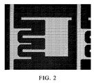
図1は、本発明のエッチング剤組成物でエッチングした後の積層物の側面図を示しており、その際、符号1はホトレジスト層を指し、符号2はCu層を指し、符号3はMo層を指し、かつ符号4はガラス基板を指す。図2は、本発明のエッチング剤組成物でエッチングした後の積層物の1000倍拡大した光学顕微鏡写真である。
(2) Etching operations Mo and Cu layers are formed on a glass substrate by physical vapor deposition in turn, and then a protective photoresist is formed on the Cu layer, which etches to form the substrate to be tested. Define the pattern. The substrate to be tested is immersed in an etchant composition having the components listed above and an etching process is performed. The detailed conditions for the etching operation are as follows:
Cu / Mo thickness: Cu 3000 mm / Mo 300 mm;
Etching temperature: 25 ° C .; and etching time: 90 seconds (3) Results FIG. 1 shows a side view of the laminate after etching with the etching agent composition of the present invention, where reference numeral 1 denotes a photoresist layer. , 2 indicates the Cu layer, 3 indicates the Mo layer, and 4 indicates the glass substrate. FIG. 2 is an optical micrograph magnified 1000 times of the laminate after etching with the etching agent composition of the present invention.
図1に示されるように、エッチング後のCu/MoワイヤのCDロスは小さい。ワイヤ側部は、傾斜台形であった。更に、Mo層からアンダーカットは観察されなかった。エッチング結果は優れていた。 As shown in FIG. 1, the CD loss of the Cu / Mo wire after etching is small. The wire side was an inclined trapezoid. Furthermore, no undercut was observed from the Mo layer. The etching result was excellent.
引き続き、ホトレジスト層を、エッチング後に試験する基板から除去する。試験する基板の走査型電子顕微鏡(SEM)の上面図を、図3に示す。図3に示されるように、Cu/Moワイヤの縁部は滑らかであった。ガラス基板の表面は清浄であり、金属残分を有さなかった。 Subsequently, the photoresist layer is removed from the substrate to be tested after etching. A top view of a scanning electron microscope (SEM) of the substrate to be tested is shown in FIG. As shown in FIG. 3, the edge of the Cu / Mo wire was smooth. The surface of the glass substrate was clean and had no metal residue.
本発明の様々な変更が可能であることはたやすく明らかとなり、当業者にはそれらはたやすく示唆され、考慮されるものである。 It will be readily apparent that various modifications of the present invention are possible and will be readily suggested and considered by those skilled in the art.
1 ホトレジスト層、 2 Cu層、 3 Mo層、 4 ガラス基板 1 photoresist layer, 2 Cu layer, 3 Mo layer, 4 glass substrate
Claims (14)
1〜25質量%の過酸化水素;
0.1〜15質量%のアミノ酸;
0.1〜15質量%のpH安定剤;
0.01〜2質量%のフッ素含有酸;
0.01〜3質量%の酸性pH調整剤;及び
水性媒体
を含有するエッチング剤組成物。 An etchant composition suitable for etching metal Cu / Mo, with respect to the total mass of the composition:
1 to 25% by weight of hydrogen peroxide;
0.1 to 15% by weight of amino acids;
0.1 to 15% by weight of a pH stabilizer;
0.01 to 2% by mass of a fluorine-containing acid;
Etching agent composition containing 0.01-3 mass% acidic pH adjuster; and an aqueous medium.
3〜20質量%の過酸化水素;
0.5〜5質量%のアミノ酸;
0.8〜3質量%のpH安定剤;
0.01〜0.3質量%のフッ素含有酸;
0.02〜0.5質量%の酸性pH調整剤;及び
水性媒体
を含有する前記エッチング剤組成物。 The etchant composition according to claim 1, wherein the total mass of the composition is:
3-20% by weight hydrogen peroxide;
0.5-5% by weight of amino acids;
0.8 to 3% by weight of a pH stabilizer;
0.01 to 0.3% by mass of a fluorine-containing acid;
The said etching agent composition containing 0.02-0.5 mass% acidic pH adjuster; and an aqueous medium.
基板を提供すること;
前記基板上にMo層を形成すること;
前記Mo層上にCu層を形成すること;
前記Cu層上にパターン形成されたマスク層を形成すること;及び
前記のCu層及びMo層を、請求項1から9までのいずれか1項に記載のエッチング剤組成物によって前記のパターン形成されたマスク層によってエッチングすること;
を含む前記方法。 In the etching method of metal Cu / Mo,
Providing a substrate;
Forming a Mo layer on the substrate;
Forming a Cu layer on the Mo layer;
A patterned mask layer is formed on the Cu layer; and the Cu layer and the Mo layer are patterned with the etchant composition according to any one of claims 1 to 9. Etching with a mask layer;
Including said method.
Applications Claiming Priority (3)
| Application Number | Priority Date | Filing Date | Title |
|---|---|---|---|
| TW96137710A TW200916605A (en) | 2007-10-08 | 2007-10-08 | Etchant compositions and etching method for metals Cu/Mo |
| CNA2007101673174A CN101418449A (en) | 2007-10-22 | 2007-10-22 | Etching liquid composition for copper/molybdenum metal and etching method |
| PCT/EP2008/063221 WO2009047203A1 (en) | 2007-10-08 | 2008-10-02 | ETCHANT COMPOSITIONS AND ETCHING METHOD FOR METALS Cu/Mo |
Publications (2)
| Publication Number | Publication Date |
|---|---|
| JP2010537444A true JP2010537444A (en) | 2010-12-02 |
| JP2010537444A5 JP2010537444A5 (en) | 2012-02-02 |
Family
ID=40219299
Family Applications (1)
| Application Number | Title | Priority Date | Filing Date |
|---|---|---|---|
| JP2010522406A Pending JP2010537444A (en) | 2007-10-08 | 2008-10-02 | Etching composition and etching method for metal Cu / Mo |
Country Status (4)
| Country | Link |
|---|---|
| US (1) | US20100301010A1 (en) |
| JP (1) | JP2010537444A (en) |
| KR (1) | KR20100064361A (en) |
| WO (1) | WO2009047203A1 (en) |
Cited By (1)
| Publication number | Priority date | Publication date | Assignee | Title |
|---|---|---|---|---|
| JP2013060634A (en) * | 2011-09-14 | 2013-04-04 | Tosoh Corp | Etching solution |
Families Citing this family (12)
| Publication number | Priority date | Publication date | Assignee | Title |
|---|---|---|---|---|
| WO2010093011A1 (en) | 2009-02-16 | 2010-08-19 | 日立化成工業株式会社 | Polishing agent for copper polishing and polishing method using same |
| US8845915B2 (en) | 2009-02-16 | 2014-09-30 | Hitachi Chemical Company, Ltd. | Abrading agent and abrading method |
| TWI405874B (en) * | 2010-02-15 | 2013-08-21 | Mitsubishi Gas Chemical Co | Etching liquid for multilayer thin films containing copper and molybdenum layers |
| KR20120066950A (en) | 2010-12-15 | 2012-06-25 | 삼성전자주식회사 | Echtant, display device and method for manufacturing display device using the same |
| KR20140013310A (en) | 2012-07-23 | 2014-02-05 | 삼성디스플레이 주식회사 | Etchant and manufacturing method of metal wiring and thin film transistor array panel using the same |
| KR20150043569A (en) * | 2013-10-07 | 2015-04-23 | 주식회사 이엔에프테크놀로지 | Etching composition for copper and molibdenum containing film |
| KR20150124540A (en) | 2014-04-28 | 2015-11-06 | 삼성디스플레이 주식회사 | Echtant and method for manufacturing display device using the same |
| KR102218353B1 (en) * | 2014-06-26 | 2021-02-22 | 동우 화인켐 주식회사 | Etching solution composition for metal layer and manufacturing method of an array substrate for Liquid crystal display using the same |
| KR102209680B1 (en) * | 2014-06-27 | 2021-01-29 | 동우 화인켐 주식회사 | Etching solution composition for metal layer and manufacturing method of an array substrate for Liquid crystal display using the same |
| TWI618817B (en) * | 2015-12-29 | 2018-03-21 | Daxin Materials Corporation | Etchant composition and etching method using thereof |
| CN117062326A (en) * | 2017-09-12 | 2023-11-14 | 株式会社东芝 | Method for manufacturing ceramic circuit board |
| EP4136273A4 (en) * | 2020-04-14 | 2024-05-01 | Entegris, Inc. | Method and composition for etching molybdenum |
Citations (4)
| Publication number | Priority date | Publication date | Assignee | Title |
|---|---|---|---|---|
| JP2004193620A (en) * | 2002-12-12 | 2004-07-08 | Lg Phillips Lcd Co Ltd | Etching solution for removing molybdenum residue from copper molybdenum film, and etching method therefore |
| WO2006138235A2 (en) * | 2005-06-13 | 2006-12-28 | Advanced Technology Materials, Inc. | Compositions and methods for selective removal of metal or metal alloy after metal silicide formation |
| JP2007005790A (en) * | 2005-06-22 | 2007-01-11 | Samsung Electronics Co Ltd | Etchant, method for forming wiring using this, and method for manufacturing thin film transistor substrate |
| WO2008121952A1 (en) * | 2007-03-31 | 2008-10-09 | Advanced Technology Materials, Inc. | Methods for stripping material for wafer reclamation |
Family Cites Families (3)
| Publication number | Priority date | Publication date | Assignee | Title |
|---|---|---|---|---|
| KR101190907B1 (en) * | 2004-12-07 | 2012-10-12 | 가오 가부시키가이샤 | Remover composition |
| TWI378989B (en) * | 2006-09-01 | 2012-12-11 | Taiwan Tft Lcd Ass | Etchant for patterning composite layer and method of fabricating thin film transistor using the same |
| KR101326128B1 (en) * | 2006-09-29 | 2013-11-06 | 삼성디스플레이 주식회사 | Wire for display device, etchant, thin film transistor array panel and method for manufacturing the same |
-
2008
- 2008-10-02 US US12/675,131 patent/US20100301010A1/en not_active Abandoned
- 2008-10-02 WO PCT/EP2008/063221 patent/WO2009047203A1/en active Application Filing
- 2008-10-02 JP JP2010522406A patent/JP2010537444A/en active Pending
- 2008-10-02 KR KR1020107004302A patent/KR20100064361A/en not_active Application Discontinuation
Patent Citations (4)
| Publication number | Priority date | Publication date | Assignee | Title |
|---|---|---|---|---|
| JP2004193620A (en) * | 2002-12-12 | 2004-07-08 | Lg Phillips Lcd Co Ltd | Etching solution for removing molybdenum residue from copper molybdenum film, and etching method therefore |
| WO2006138235A2 (en) * | 2005-06-13 | 2006-12-28 | Advanced Technology Materials, Inc. | Compositions and methods for selective removal of metal or metal alloy after metal silicide formation |
| JP2007005790A (en) * | 2005-06-22 | 2007-01-11 | Samsung Electronics Co Ltd | Etchant, method for forming wiring using this, and method for manufacturing thin film transistor substrate |
| WO2008121952A1 (en) * | 2007-03-31 | 2008-10-09 | Advanced Technology Materials, Inc. | Methods for stripping material for wafer reclamation |
Cited By (1)
| Publication number | Priority date | Publication date | Assignee | Title |
|---|---|---|---|---|
| JP2013060634A (en) * | 2011-09-14 | 2013-04-04 | Tosoh Corp | Etching solution |
Also Published As
| Publication number | Publication date |
|---|---|
| KR20100064361A (en) | 2010-06-14 |
| WO2009047203A1 (en) | 2009-04-16 |
| US20100301010A1 (en) | 2010-12-02 |
Similar Documents
| Publication | Publication Date | Title |
|---|---|---|
| JP2010537444A (en) | Etching composition and etching method for metal Cu / Mo | |
| JP5913869B2 (en) | Etching solution composition and etching method | |
| JP2010537444A5 (en) | ||
| JP4815406B2 (en) | Silicon oxide film selective wet etching solution and etching method | |
| TWI816635B (en) | Liquid composition for cleaning semiconductor components, cleaning method for semiconductor components, and manufacturing method for semiconductor components | |
| JPH09181028A (en) | Washing solution of semiconductor chip | |
| JP2007005656A (en) | Etchant composition for metal material and method of manufacturing semiconductor device using same | |
| WO2006068091A1 (en) | Fine treatment agent and fine treatment method using same | |
| TWI460311B (en) | Nickel-chromium alloy stripper for flexible wiring boards | |
| CN106555187B (en) | Etchant composition, method for etching copper-based metal layer, method for manufacturing array substrate and array substrate manufactured by same | |
| JP4428995B2 (en) | Etching solution composition for metal film | |
| JP2005162893A5 (en) | ||
| JP4632038B2 (en) | Copper wiring board manufacturing method | |
| JP6485587B1 (en) | Etching solution | |
| JP2004325918A (en) | Remover composition | |
| JP6378271B2 (en) | Tungsten film etchant composition, method for producing electronic device using the same, and electronic device | |
| JP2006191002A (en) | Remover composition | |
| WO2021210458A1 (en) | Etching liquid for titanium and/or titanium alloy, method for etching titanium and/or titanium alloy with use of said etching liquid, and method for producing substrate with use of said etching liquid | |
| JP2008216843A (en) | Photoresist stripping liquid composition | |
| TWI759450B (en) | Etching solution, etching method, and manufacturing method of display device | |
| JP6458913B1 (en) | Etching solution | |
| TWI660030B (en) | Etchant composition for copper-containing metal | |
| WO2011009764A1 (en) | Etchant composition and etching process for titanium-aluminum complex metal layer | |
| JP4577095B2 (en) | Etching composition for metal titanium and etching method using the same | |
| JP2013060634A (en) | Etching solution |
Legal Events
| Date | Code | Title | Description |
|---|---|---|---|
| RD04 | Notification of resignation of power of attorney |
Free format text: JAPANESE INTERMEDIATE CODE: A7424 Effective date: 20101228 |
|
| A521 | Written amendment |
Free format text: JAPANESE INTERMEDIATE CODE: A523 Effective date: 20111206 |
|
| A977 | Report on retrieval |
Free format text: JAPANESE INTERMEDIATE CODE: A971007 Effective date: 20120130 |
|
| A131 | Notification of reasons for refusal |
Free format text: JAPANESE INTERMEDIATE CODE: A131 Effective date: 20120203 |
|
| A02 | Decision of refusal |
Free format text: JAPANESE INTERMEDIATE CODE: A02 Effective date: 20120628 |