JP2010509769A - 発光ダイオードアセンブリ及び製造方法 - Google Patents
発光ダイオードアセンブリ及び製造方法 Download PDFInfo
- Publication number
- JP2010509769A JP2010509769A JP2009536220A JP2009536220A JP2010509769A JP 2010509769 A JP2010509769 A JP 2010509769A JP 2009536220 A JP2009536220 A JP 2009536220A JP 2009536220 A JP2009536220 A JP 2009536220A JP 2010509769 A JP2010509769 A JP 2010509769A
- Authority
- JP
- Japan
- Prior art keywords
- led
- lens
- light emitting
- array
- emitting surface
- Prior art date
- Legal status (The legal status is an assumption and is not a legal conclusion. Google has not performed a legal analysis and makes no representation as to the accuracy of the status listed.)
- Pending
Links
Images


Classifications
-
- H—ELECTRICITY
- H01—ELECTRIC ELEMENTS
- H01L—SEMICONDUCTOR DEVICES NOT COVERED BY CLASS H10
- H01L33/00—Semiconductor devices with at least one potential-jump barrier or surface barrier specially adapted for light emission; Processes or apparatus specially adapted for the manufacture or treatment thereof or of parts thereof; Details thereof
- H01L33/48—Semiconductor devices with at least one potential-jump barrier or surface barrier specially adapted for light emission; Processes or apparatus specially adapted for the manufacture or treatment thereof or of parts thereof; Details thereof characterised by the semiconductor body packages
- H01L33/52—Encapsulations
- H01L33/54—Encapsulations having a particular shape
-
- H—ELECTRICITY
- H01—ELECTRIC ELEMENTS
- H01L—SEMICONDUCTOR DEVICES NOT COVERED BY CLASS H10
- H01L25/00—Assemblies consisting of a plurality of individual semiconductor or other solid state devices ; Multistep manufacturing processes thereof
- H01L25/03—Assemblies consisting of a plurality of individual semiconductor or other solid state devices ; Multistep manufacturing processes thereof all the devices being of a type provided for in the same subgroup of groups H01L27/00 - H01L33/00, or in a single subclass of H10K, H10N, e.g. assemblies of rectifier diodes
- H01L25/04—Assemblies consisting of a plurality of individual semiconductor or other solid state devices ; Multistep manufacturing processes thereof all the devices being of a type provided for in the same subgroup of groups H01L27/00 - H01L33/00, or in a single subclass of H10K, H10N, e.g. assemblies of rectifier diodes the devices not having separate containers
- H01L25/075—Assemblies consisting of a plurality of individual semiconductor or other solid state devices ; Multistep manufacturing processes thereof all the devices being of a type provided for in the same subgroup of groups H01L27/00 - H01L33/00, or in a single subclass of H10K, H10N, e.g. assemblies of rectifier diodes the devices not having separate containers the devices being of a type provided for in group H01L33/00
- H01L25/0753—Assemblies consisting of a plurality of individual semiconductor or other solid state devices ; Multistep manufacturing processes thereof all the devices being of a type provided for in the same subgroup of groups H01L27/00 - H01L33/00, or in a single subclass of H10K, H10N, e.g. assemblies of rectifier diodes the devices not having separate containers the devices being of a type provided for in group H01L33/00 the devices being arranged next to each other
-
- H—ELECTRICITY
- H01—ELECTRIC ELEMENTS
- H01L—SEMICONDUCTOR DEVICES NOT COVERED BY CLASS H10
- H01L2924/00—Indexing scheme for arrangements or methods for connecting or disconnecting semiconductor or solid-state bodies as covered by H01L24/00
- H01L2924/0001—Technical content checked by a classifier
- H01L2924/0002—Not covered by any one of groups H01L24/00, H01L24/00 and H01L2224/00
-
- H—ELECTRICITY
- H01—ELECTRIC ELEMENTS
- H01L—SEMICONDUCTOR DEVICES NOT COVERED BY CLASS H10
- H01L33/00—Semiconductor devices with at least one potential-jump barrier or surface barrier specially adapted for light emission; Processes or apparatus specially adapted for the manufacture or treatment thereof or of parts thereof; Details thereof
- H01L33/48—Semiconductor devices with at least one potential-jump barrier or surface barrier specially adapted for light emission; Processes or apparatus specially adapted for the manufacture or treatment thereof or of parts thereof; Details thereof characterised by the semiconductor body packages
- H01L33/50—Wavelength conversion elements
Landscapes
- Engineering & Computer Science (AREA)
- Microelectronics & Electronic Packaging (AREA)
- Manufacturing & Machinery (AREA)
- Computer Hardware Design (AREA)
- Power Engineering (AREA)
- Led Device Packages (AREA)
Abstract
Description

本発明の一つの実施態様では、レンズアレイの個々の要素(レンズ)は、LEDウェハ上のLEDダイスのサイズに実質的に合致する寸法を有することができ、特に、各アレイ要素は、対応するLEDダイスの発光面に投影された断面積がLEDの発光面の面積に実質的に等しい又はそれ未満である1個のレンズを含んでいる。このような構成では、レンズとチップとが一対一に対応して対をなす。あるいはまた、レンズアレイ中の個々のレンズの寸法は、LEDウェハ上の対応するダイスの外周よりも大きくてもよい。これらはまた、空間的に互いに合うようにして、レンズのサイズが約50μmから約5mmまでの範囲とすることもできる。レンズアレイの要素とLEDアレイのLEDダイスとのこの一対一の合致が図1に示されている。
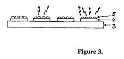
本LEDレンズアセンブリを製造する例示的な方法が図5(a)〜5(g)に示されている。この例では、レンズアレイがウェハ上のLEDダイスのアレイであって、二つのアレイの間にリン光体層は介在しないアレイに適合されている。ウェハ上のLEDアレイの上にレンズアレイを製造するために用いられる一つの方法は、リソグラフィー刷込み(インプリンティング)法である。図5(a)は、一つ以上の電極領域6を有するLEDウェハ3を示す。LEDアレイの個々のLEDは図5に示されていないことに留意すべきである。
ステップ1―図5(b)
透明なレンズ材料7がLEDウェハ3の上に塗布される又はさもなくば配置される。透明なレンズ材料7は、シリコーン、エポキシ、ポリマー、ガラス、プラスチック材料又はそれらの混合物であり得る。
材料をスタンプ8の形状にさせるために、透明なレンズ材料からレンズを成形するようにデザインされたパターンを有するスタンプ8を透明なレンズ材料7に適用する。図示された実施態様では、LEDウェハの各LEDダイスに対応する1個のレンズが存在している。スタンプ8はまた、LEDアレイの一つ以上の電極6へのその後の電気的アクセスを可能にするための電極ウィンドウパターン9を提供するように構成されている。
レンズ材料をUV線10又は熱処理にさらし、パターン化されたレンズアレイ及び電極ウィンドウを硬化させる(このステップは省略可能であり、使用されるレンズ材料に依存する)。レンズ材料をUVにさらすことを可能にするために、マスク8は、有利には、UV放射に対して透過性である材料でできている。
スタンプ8を除去する。
残留ケイ素又はエポキシレンズ材料をアッシングするため、及び/又はLEDを駆動し、制御するために必要な電極6への電気的アクセスを提供するために、透明な材料の選択領域9をエッチング、たとえば酸素プラズマ又はウェットエッチングにさらす。図5(g)は、完成したLEDレンズアセンブリを示す平面図である。
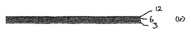
ステップ1―図6(b)
リン光体層12をLEDウェハ3全体の上に塗布する又はさもなくば配置する。
透明なレンズ材料7をリン光体層12の上に塗布する又はさもなくば配置する。ある実施態様では、透明なレンズ材料は、シリコーン、エポキシ、ポリマー、プラスチック材料、ガラス又はそれらの混合物である。
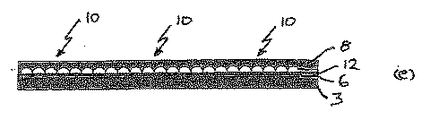
材料をスタンプ8の形状にさせるために、透明なレンズ材料からレンズを成形するようにデザインされたパターンを有するスタンプ8を透明なレンズ材料7に適用する。図示された実施態様では、LEDウェハの各LEDダイスに対応する1個のレンズが存在している。スタンプ8はまた、LEDアレイの一つ以上の電極6へのその後の電気的アクセスを可能にするための電極ウィンドウパターン9を提供するように構成されている。
レンズ材料をUV線10又は熱処理にさらし、パターン化されたレンズアレイ及び電極ウィンドウを硬化させる(このステップは省略可能であり、使用されるレンズ材料に依存する)。
スタンプ8を除去する。
場合によっては、残留ケイ素、リン光体又はエポキシレンズ材料をアッシングするため、及び/又はLEDを駆動し、制御するための電極6への電気的アクセスを提供するために、透明な材料の選択領域をエッチング、たとえば酸素プラズマ又はウェットエッチングにさらす。図6(h)は、完成したLEDレンズアセンブリを示す平面図である。
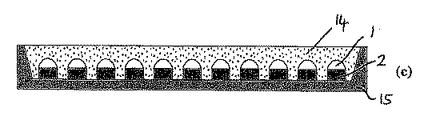
LEDレンズ装置(個々のアセンブリ及び適合されたアレイパターン)に付随するリン光体を構成する代替方法が、図7及び8に示されている。図7(a)〜7(d)に示す構成では、リン光体14が透明なマトリックス材料(たとえばエポキシ)中に埋め込まれ、LEDレンズアセンブリ2、1及び/又は適合されたレンズアレイ及びLEDアレイ5、2そのものが、ハウジング15内部のリン光/マトリックス材料14中に埋め込まれ、リン光/マトリックス材料14に包囲される。よって、図7(a)〜7(d)に示されている構成では、LED2からの光は、リン光体含浸エポキシ又はシリコーン材料14に入射する前に、LEDに付随するレンズ1によって集束及び/又は増強され、リン光体含浸エポキシ又はシリコーン材料14で光は、1)リン光体を励起し、2)リン光体によって発っせられた光と組み合わさって最終生成光を形成する。
Claims (20)
- LED2及びLEDの発光面に隣接して配置されたレンズ1を含むLEDアセンブリであって、LEDの発光面に投影されるレンズの断面積がLEDの発光面の面積に実質的に等しいか又はそれ未満であることを特徴とするLEDアセンブリ。
- 透明な材料の中に封入されたリン光体14をさらに含み、その透明な材料がLEDの発光面の少なくとも一部分を包囲している、請求項1記載のLEDアセンブリ。
- レンズとLEDの発光面の少なくとも一部分との間に配置されたリン光体層4をさらに含む、請求項1記載のLEDアセンブリ。
- LED2の発光面に隣接して配置された少なくとも二つのレンズ5を含むLEDアセンブリであって、LEDの発光面に投影されるレンズの断面積がLEDの発光面の面積に実質的に等しいか又はそれ未満であることを特徴とするLEDアセンブリ。
- 透明な材料の中に封入されたリン光体14をさらに含み、透明な材料がLEDの発光面の少なくとも一部分を包囲している、請求項4記載のLEDアセンブリ。
- 前記少なくとも二つのレンズとLEDの発光面の少なくとも一部分との間に配置されたリン光体層4をさらに含む、請求項4記載のLEDアセンブリ。
- LEDのアレイ及びレンズのアレイを含み、LEDアレイの各メンバーに付随する少なくとも一つのレンズが存在する発光装置であって、その付随するLEDの発光面に投影された各レンズの断面積がLEDの発光面の面積に実質的に等しい又はそれ未満であることを特徴とする発光装置。
- 透明な材料の中に封入されたリン光体をさらに含み、その透明な材料がレンズアレイの少なくとも一部分を包囲している、請求項7記載の発光装置。
- レンズアレイのレンズの少なくとも一つとLEDアレイのLEDの少なくとも一つとの間に配置されたリン光体層をさらに含む、請求項7記載の発光装置。
- 発光面から第一の波長で放射を発するように構成されたLEDと、LEDからの放射を光学的に集束させるように構成されたレンズと、LEDに隣接して配置され、LEDによって発された放射の少なくとも一部分を吸収し、第二の波長で放射を発するように構成されたリン光体と、を含むフォトニック装置であって、LEDの発光面に投影されるレンズの断面積がLEDの発光面の面積に実質的に等しい又はそれ未満であることを特徴とする装置。
- リン光体が透明な材料の中に封入され、その透明な材料がLEDの発光面の少なくとも一部分を包囲している、請求項10記載のフォトニック装置。
- リン光体がレンズとLEDの発光面の少なくとも一部分との間に層として配置される、請求項10記載のフォトニック装置。
- LEDアセンブリを製造する方法であって、a)LEDアレイを含む基板の上に透明なレンズ材料を配置するステップと、及びb)透明なレンズ材料を、所望のレンズパターンに成形し、LEDアレイのパターンに適合させるステップと、を含む方法。
- 透明なレンズ材料を硬化させるステップをさらに含み、そのステップが、UV硬化ステップ及び熱硬化ステップからなる群より選択される、請求項13記載の方法。
- LEDアレイの電極への電気的アクセスを提供するために、透明なレンズ材料の選択領域を除去するステップをさらに含む、請求項13又は14記載の方法。
- エッチング、酸素プラズマエッチング及びウェットエッチングからなる群より選択される工程によって透明なレンズ材料の選択領域を除去するステップを含む、請求項15記載の方法。
- LEDアレイ基板上に透明なレンズ材料を配置する前に、LEDアレイ基板の実質的に全面にわたってリン光体層を配置するステップをさらに含む、請求項13乃至16のいずれか1項記載の方法。
- リン光体を配置する前に、LEDアレイの電極領域を覆う離型剤を提供するステップをさらに含む、請求項17記載の方法。
- LEDアレイの電極領域への電気的アクセスを提供するために、離型剤を処理し、リフトオフ工程を使用してリン光体層及び透明なレンズ材料の選択領域を除去するステップをさらに含む、請求項18記載の方法。
- 成形されたレンズ材料及びLEDアレイを、リン光体を含む透明なマトリックスに埋め込むステップをさらに含む、請求項13乃至16のいずれか1項記載の方法。
Applications Claiming Priority (3)
| Application Number | Priority Date | Filing Date | Title |
|---|---|---|---|
| US85821106P | 2006-11-09 | 2006-11-09 | |
| US11/800,977 US7737636B2 (en) | 2006-11-09 | 2007-05-07 | LED assembly with an LED and adjacent lens and method of making same |
| PCT/US2007/011187 WO2008063216A2 (en) | 2006-11-09 | 2007-05-08 | Light emitting diode assembly and method of fabrication |
Publications (2)
| Publication Number | Publication Date |
|---|---|
| JP2010509769A true JP2010509769A (ja) | 2010-03-25 |
| JP2010509769A5 JP2010509769A5 (ja) | 2010-05-06 |
Family
ID=39368374
Family Applications (1)
| Application Number | Title | Priority Date | Filing Date |
|---|---|---|---|
| JP2009536220A Pending JP2010509769A (ja) | 2006-11-09 | 2007-05-08 | 発光ダイオードアセンブリ及び製造方法 |
Country Status (5)
| Country | Link |
|---|---|
| US (1) | US7737636B2 (ja) |
| EP (1) | EP2098099A4 (ja) |
| JP (1) | JP2010509769A (ja) |
| KR (1) | KR20090082469A (ja) |
| WO (1) | WO2008063216A2 (ja) |
Families Citing this family (42)
| Publication number | Priority date | Publication date | Assignee | Title |
|---|---|---|---|---|
| US8035612B2 (en) * | 2002-05-28 | 2011-10-11 | Intellectual Ventures Holding 67 Llc | Self-contained interactive video display system |
| US8300042B2 (en) | 2001-06-05 | 2012-10-30 | Microsoft Corporation | Interactive video display system using strobed light |
| US7710391B2 (en) * | 2002-05-28 | 2010-05-04 | Matthew Bell | Processing an image utilizing a spatially varying pattern |
| US20050122308A1 (en) * | 2002-05-28 | 2005-06-09 | Matthew Bell | Self-contained interactive video display system |
| AU2003301043A1 (en) * | 2002-12-13 | 2004-07-09 | Reactrix Systems | Interactive directed light/sound system |
| CN1902930B (zh) | 2003-10-24 | 2010-12-15 | 瑞克楚斯系统公司 | 管理交互式视频显示系统的方法和系统 |
| US9128519B1 (en) | 2005-04-15 | 2015-09-08 | Intellectual Ventures Holding 67 Llc | Method and system for state-based control of objects |
| US8081822B1 (en) | 2005-05-31 | 2011-12-20 | Intellectual Ventures Holding 67 Llc | System and method for sensing a feature of an object in an interactive video display |
| US8098277B1 (en) | 2005-12-02 | 2012-01-17 | Intellectual Ventures Holding 67 Llc | Systems and methods for communication between a reactive video system and a mobile communication device |
| US20080064131A1 (en) * | 2006-09-12 | 2008-03-13 | Mutual-Tek Industries Co., Ltd. | Light emitting apparatus and method for the same |
| JP2009032882A (ja) * | 2007-07-26 | 2009-02-12 | Sanken Electric Co Ltd | 半導体発光素子及び半導体発光素子製造方法 |
| AU2008299883B2 (en) | 2007-09-14 | 2012-03-15 | Facebook, Inc. | Processing of gesture-based user interactions |
| KR101361575B1 (ko) * | 2007-09-17 | 2014-02-13 | 삼성전자주식회사 | 발광 다이오드 패키지 및 그 제조방법 |
| US8159682B2 (en) | 2007-11-12 | 2012-04-17 | Intellectual Ventures Holding 67 Llc | Lens system |
| TW201442280A (zh) * | 2007-11-30 | 2014-11-01 | Univ California | 利用表面粗糙之高度光取出效率之氮化物基發光二極體 |
| US20100039500A1 (en) * | 2008-02-15 | 2010-02-18 | Matthew Bell | Self-Contained 3D Vision System Utilizing Stereo Camera and Patterned Illuminator |
| US8259163B2 (en) | 2008-03-07 | 2012-09-04 | Intellectual Ventures Holding 67 Llc | Display with built in 3D sensing |
| US8595218B2 (en) | 2008-06-12 | 2013-11-26 | Intellectual Ventures Holding 67 Llc | Interactive display management systems and methods |
| KR101039957B1 (ko) * | 2008-11-18 | 2011-06-09 | 엘지이노텍 주식회사 | 발광 장치 및 이를 구비한 디스플레이 장치 |
| TWI462350B (zh) * | 2008-12-24 | 2014-11-21 | Ind Tech Res Inst | 多晶發光二極體 |
| US20110089447A1 (en) * | 2009-10-19 | 2011-04-21 | Wu-Cheng Kuo | Light-emiting device chip with micro-lenses and method for fabricating the same |
| KR20110043864A (ko) * | 2009-10-22 | 2011-04-28 | 포항공과대학교 산학협력단 | 색 혼합 렌즈 및 이를 가지는 액정 표시 장치 |
| US10500770B2 (en) * | 2010-03-02 | 2019-12-10 | So-Semi Technologies, Llc | LED packaging with integrated optics and methods of manufacturing the same |
| CN101814572A (zh) * | 2010-03-05 | 2010-08-25 | 矽畿科技股份有限公司 | 光二极管封装结构 |
| CN102906877A (zh) * | 2010-05-27 | 2013-01-30 | 奥斯兰姆施尔凡尼亚公司 | 包括全氮化物发光二极管的发光二极管光源 |
| JP2012028749A (ja) * | 2010-07-22 | 2012-02-09 | Seoul Opto Devices Co Ltd | 発光ダイオード |
| TW201208143A (en) * | 2010-08-06 | 2012-02-16 | Semileds Optoelectronics Co | White LED device and manufacturing method thereof |
| US8534901B2 (en) | 2010-09-13 | 2013-09-17 | Teledyne Reynolds, Inc. | Collimating waveguide apparatus and method |
| US8608328B2 (en) | 2011-05-06 | 2013-12-17 | Teledyne Technologies Incorporated | Light source with secondary emitter conversion element |
| DE102011078572B4 (de) * | 2011-07-04 | 2016-06-02 | Osram Gmbh | Beleuchtungsvorrichtung |
| US9115865B1 (en) | 2012-06-19 | 2015-08-25 | Forever Gifts, Inc. | Lighting device having light-distributing void |
| US20140307431A1 (en) * | 2013-04-16 | 2014-10-16 | Xeralux, Inc. | Field Configurable Industrial LED Light Fixture |
| DE102013209919A1 (de) * | 2013-05-28 | 2014-12-04 | Osram Opto Semiconductors Gmbh | Optoelektronisches Bauelement mit einem Gehäuse mit mehreren Öffnungen |
| US20150133753A1 (en) * | 2013-11-14 | 2015-05-14 | General Electric Company | Arrays of emitters for pulse oximetry devices and methods of making the same |
| US9465175B2 (en) * | 2014-07-23 | 2016-10-11 | Sifotonics Technologies Co., Ltd. | Integrated lens-array-on-substrate for optical coupling system and fabrication method thereof |
| US10066160B2 (en) | 2015-05-01 | 2018-09-04 | Intematix Corporation | Solid-state white light generating lighting arrangements including photoluminescence wavelength conversion components |
| US20180073686A1 (en) * | 2016-09-14 | 2018-03-15 | Osram Sylvania Inc. | Solid state lighting device with electronically adjustable light beam distribution |
| DE102016224090B4 (de) * | 2016-12-05 | 2024-03-28 | OSRAM Opto Semiconductors Gesellschaft mit beschränkter Haftung | Optoelektronisches Bauelement, Modul mit mindestens zwei optoelektronischen Bauelementen und Verfahren zum Herstellen eines optoelektronischen Bauelements |
| DE102018101786A1 (de) * | 2018-01-26 | 2019-08-01 | Osram Opto Semiconductors Gmbh | Lichtemittierendes Halbleiterbauteil |
| CN109411460B (zh) * | 2018-12-20 | 2024-03-29 | 广州美锐健康产业股份有限公司 | 多光谱固态发光器件及多光谱照射光源 |
| KR20210083587A (ko) | 2019-12-27 | 2021-07-07 | 에스엘 주식회사 | 렌즈어셈블리 및 이의 제작방법 |
| KR20220048604A (ko) * | 2020-10-13 | 2022-04-20 | 주식회사 루멘스 | 칩 스케일 패키지 엘이디 및 그 제조방법 |
Citations (12)
| Publication number | Priority date | Publication date | Assignee | Title |
|---|---|---|---|---|
| JPH04239781A (ja) * | 1991-01-23 | 1992-08-27 | Eastman Kodak Japan Kk | Ledアレイチップ |
| JPH05251485A (ja) * | 1992-03-06 | 1993-09-28 | Sharp Corp | 発光装置のレンズ成形方法 |
| JPH06151972A (ja) * | 1992-11-09 | 1994-05-31 | Omron Corp | レンズ・オン・チップ型発光装置及びその製造方法 |
| JPH1146015A (ja) * | 1997-07-28 | 1999-02-16 | Nichia Chem Ind Ltd | 発光ダイオード及びその形成方法 |
| JP2001111109A (ja) * | 1999-10-07 | 2001-04-20 | Sharp Corp | 窒化ガリウム系化合物半導体発光素子 |
| JP2003209286A (ja) * | 2001-11-08 | 2003-07-25 | Nichia Chem Ind Ltd | 発光装置およびその製造方法 |
| JP2005109059A (ja) * | 2003-09-30 | 2005-04-21 | Sanyo Electric Co Ltd | 発光素子およびその製造方法 |
| JP2005175417A (ja) * | 2003-07-28 | 2005-06-30 | Ricoh Co Ltd | 発光素子アレイ、光書込ユニットおよび画像形成装置 |
| JP2005268431A (ja) * | 2004-03-17 | 2005-09-29 | Nichia Chem Ind Ltd | 発光装置及びその製造方法 |
| WO2006038648A1 (ja) * | 2004-10-06 | 2006-04-13 | Matsushita Electric Industrial Co., Ltd. | マイクロレンズ、マイクロレンズアレイ及びその製造方法 |
| JP2006190955A (ja) * | 2004-12-30 | 2006-07-20 | Ind Technol Res Inst | 準全方向反射器を有する発光ダイオード |
| WO2006089508A1 (de) * | 2005-02-28 | 2006-08-31 | Osram Opto Semiconductors Gmbh | Led-array |
Family Cites Families (7)
| Publication number | Priority date | Publication date | Assignee | Title |
|---|---|---|---|---|
| JPH07115244A (ja) * | 1993-10-19 | 1995-05-02 | Toyota Motor Corp | 半導体レーザー及びその製造方法 |
| US5803579A (en) * | 1996-06-13 | 1998-09-08 | Gentex Corporation | Illuminator assembly incorporating light emitting diodes |
| US6501091B1 (en) * | 1998-04-01 | 2002-12-31 | Massachusetts Institute Of Technology | Quantum dot white and colored light emitting diodes |
| US6429583B1 (en) * | 1998-11-30 | 2002-08-06 | General Electric Company | Light emitting device with ba2mgsi2o7:eu2+, ba2sio4:eu2+, or (srxcay ba1-x-y)(a1zga1-z)2sr:eu2+phosphors |
| US7374807B2 (en) * | 2004-01-15 | 2008-05-20 | Nanosys, Inc. | Nanocrystal doped matrixes |
| JP2006049657A (ja) * | 2004-08-06 | 2006-02-16 | Citizen Electronics Co Ltd | Ledランプ |
| KR100790741B1 (ko) | 2006-09-07 | 2008-01-02 | 삼성전기주식회사 | 엘이디 패키지용 렌즈의 제작 방법 |
-
2007
- 2007-05-07 US US11/800,977 patent/US7737636B2/en not_active Expired - Fee Related
- 2007-05-08 WO PCT/US2007/011187 patent/WO2008063216A2/en active Application Filing
- 2007-05-08 JP JP2009536220A patent/JP2010509769A/ja active Pending
- 2007-05-08 KR KR1020097011885A patent/KR20090082469A/ko active Search and Examination
- 2007-05-08 EP EP07794684A patent/EP2098099A4/en not_active Withdrawn
Patent Citations (12)
| Publication number | Priority date | Publication date | Assignee | Title |
|---|---|---|---|---|
| JPH04239781A (ja) * | 1991-01-23 | 1992-08-27 | Eastman Kodak Japan Kk | Ledアレイチップ |
| JPH05251485A (ja) * | 1992-03-06 | 1993-09-28 | Sharp Corp | 発光装置のレンズ成形方法 |
| JPH06151972A (ja) * | 1992-11-09 | 1994-05-31 | Omron Corp | レンズ・オン・チップ型発光装置及びその製造方法 |
| JPH1146015A (ja) * | 1997-07-28 | 1999-02-16 | Nichia Chem Ind Ltd | 発光ダイオード及びその形成方法 |
| JP2001111109A (ja) * | 1999-10-07 | 2001-04-20 | Sharp Corp | 窒化ガリウム系化合物半導体発光素子 |
| JP2003209286A (ja) * | 2001-11-08 | 2003-07-25 | Nichia Chem Ind Ltd | 発光装置およびその製造方法 |
| JP2005175417A (ja) * | 2003-07-28 | 2005-06-30 | Ricoh Co Ltd | 発光素子アレイ、光書込ユニットおよび画像形成装置 |
| JP2005109059A (ja) * | 2003-09-30 | 2005-04-21 | Sanyo Electric Co Ltd | 発光素子およびその製造方法 |
| JP2005268431A (ja) * | 2004-03-17 | 2005-09-29 | Nichia Chem Ind Ltd | 発光装置及びその製造方法 |
| WO2006038648A1 (ja) * | 2004-10-06 | 2006-04-13 | Matsushita Electric Industrial Co., Ltd. | マイクロレンズ、マイクロレンズアレイ及びその製造方法 |
| JP2006190955A (ja) * | 2004-12-30 | 2006-07-20 | Ind Technol Res Inst | 準全方向反射器を有する発光ダイオード |
| WO2006089508A1 (de) * | 2005-02-28 | 2006-08-31 | Osram Opto Semiconductors Gmbh | Led-array |
Also Published As
| Publication number | Publication date |
|---|---|
| WO2008063216A3 (en) | 2008-10-30 |
| EP2098099A4 (en) | 2012-10-10 |
| US7737636B2 (en) | 2010-06-15 |
| WO2008063216A2 (en) | 2008-05-29 |
| KR20090082469A (ko) | 2009-07-30 |
| US20080111141A1 (en) | 2008-05-15 |
| EP2098099A2 (en) | 2009-09-09 |
Similar Documents
| Publication | Publication Date | Title |
|---|---|---|
| JP2010509769A (ja) | 発光ダイオードアセンブリ及び製造方法 | |
| US7863635B2 (en) | Semiconductor light emitting devices with applied wavelength conversion materials | |
| US8564004B2 (en) | Complex primary optics with intermediate elements | |
| EP2279535B1 (en) | Semiconductor light emitting devices with separated wavelength conversion materials and methods of forming the same | |
| KR102222215B1 (ko) | 기판내에 산란 특징을 갖는 led | |
| JP5243436B2 (ja) | 半導体チップおよび半導体チップの製造方法 | |
| US20150014708A1 (en) | Package for light emitting and receiving devices | |
| KR20160029030A (ko) | 광전자 컴포넌트를 제조하기 위한 방법 | |
| KR20180127292A (ko) | 경사 반사기를 갖는 발광 디바이스 및 그 제조 방법 | |
| TWI497774B (zh) | 發光元件及其製造方法 | |
| TWI636584B (zh) | 發光二極體組件、包括該發光二極體組件的發光二極體、及微光學多層結構 | |
| KR20090002835A (ko) | 질화물계 발광 소자 및 그 제조방법 | |
| JP2012529766A (ja) | 遠隔の蛍燐光体の層及び反射性のサブマウントを備えたled | |
| KR20130093640A (ko) | 발광 변환 물질 층을 형성하는 방법, 발광 변환 물질 층을 위한 조성물 및 발광 변환 물질 층을 포함하는 소자 | |
| TW202101730A (zh) | 超光滑側壁畫素陣列led | |
| TWI381522B (zh) | 發光二極體組件及其製造方法 | |
| KR20190092556A (ko) | 높은 근거리 콘트라스트 비를 갖는 led 모듈 | |
| US20230106479A1 (en) | Lumiphoric material arrangements for multiple-junction light-emitting diodes | |
| TWI835720B (zh) | 發光二極體模組及其製造方法及相關之閃光燈模組、汽車頭燈或投影發光二極體系統 | |
| KR20230138023A (ko) | 광학 배열을 갖는 커버 구조를 갖는 발광 다이오드 패키지 및 제조 방법 | |
| WO2023046431A1 (en) | Semiconductor light source, cover body and method to produce the same |
Legal Events
| Date | Code | Title | Description |
|---|---|---|---|
| A521 | Written amendment |
Free format text: JAPANESE INTERMEDIATE CODE: A523 Effective date: 20100302 |
|
| A621 | Written request for application examination |
Free format text: JAPANESE INTERMEDIATE CODE: A621 Effective date: 20100302 |
|
| A977 | Report on retrieval |
Free format text: JAPANESE INTERMEDIATE CODE: A971007 Effective date: 20120312 |
|
| A131 | Notification of reasons for refusal |
Free format text: JAPANESE INTERMEDIATE CODE: A131 Effective date: 20120508 |
|
| A521 | Written amendment |
Free format text: JAPANESE INTERMEDIATE CODE: A523 Effective date: 20120808 |
|
| A131 | Notification of reasons for refusal |
Free format text: JAPANESE INTERMEDIATE CODE: A131 Effective date: 20130226 |
|
| A601 | Written request for extension of time |
Free format text: JAPANESE INTERMEDIATE CODE: A601 Effective date: 20130515 |
|
| A602 | Written permission of extension of time |
Free format text: JAPANESE INTERMEDIATE CODE: A602 Effective date: 20130522 |
|
| A601 | Written request for extension of time |
Free format text: JAPANESE INTERMEDIATE CODE: A601 Effective date: 20130626 |
|
| RD03 | Notification of appointment of power of attorney |
Free format text: JAPANESE INTERMEDIATE CODE: A7423 Effective date: 20130626 |
|
| A521 | Written amendment |
Free format text: JAPANESE INTERMEDIATE CODE: A523 Effective date: 20130726 |
|
| A601 | Written request for extension of time |
Free format text: JAPANESE INTERMEDIATE CODE: A601 Effective date: 20130726 |
|
| A602 | Written permission of extension of time |
Free format text: JAPANESE INTERMEDIATE CODE: A602 Effective date: 20130802 |
|
| A521 | Written amendment |
Free format text: JAPANESE INTERMEDIATE CODE: A523 Effective date: 20130826 |
|
| RD04 | Notification of resignation of power of attorney |
Free format text: JAPANESE INTERMEDIATE CODE: A7424 Effective date: 20130816 |
|
| A02 | Decision of refusal |
Free format text: JAPANESE INTERMEDIATE CODE: A02 Effective date: 20131001 |