JP2010171402A - Thermosetting die-bonding film - Google Patents
Thermosetting die-bonding film Download PDFInfo
- Publication number
- JP2010171402A JP2010171402A JP2009288001A JP2009288001A JP2010171402A JP 2010171402 A JP2010171402 A JP 2010171402A JP 2009288001 A JP2009288001 A JP 2009288001A JP 2009288001 A JP2009288001 A JP 2009288001A JP 2010171402 A JP2010171402 A JP 2010171402A
- Authority
- JP
- Japan
- Prior art keywords
- die
- film
- thermosetting
- weight
- resin
- Prior art date
- Legal status (The legal status is an assumption and is not a legal conclusion. Google has not performed a legal analysis and makes no representation as to the accuracy of the status listed.)
- Pending
Links
Images


Classifications
-
- H—ELECTRICITY
- H01—ELECTRIC ELEMENTS
- H01L—SEMICONDUCTOR DEVICES NOT COVERED BY CLASS H10
- H01L24/00—Arrangements for connecting or disconnecting semiconductor or solid-state bodies; Methods or apparatus related thereto
- H01L24/01—Means for bonding being attached to, or being formed on, the surface to be connected, e.g. chip-to-package, die-attach, "first-level" interconnects; Manufacturing methods related thereto
- H01L24/26—Layer connectors, e.g. plate connectors, solder or adhesive layers; Manufacturing methods related thereto
- H01L24/28—Structure, shape, material or disposition of the layer connectors prior to the connecting process
- H01L24/29—Structure, shape, material or disposition of the layer connectors prior to the connecting process of an individual layer connector
-
- H—ELECTRICITY
- H01—ELECTRIC ELEMENTS
- H01L—SEMICONDUCTOR DEVICES NOT COVERED BY CLASS H10
- H01L23/00—Details of semiconductor or other solid state devices
- H01L23/28—Encapsulations, e.g. encapsulating layers, coatings, e.g. for protection
- H01L23/31—Encapsulations, e.g. encapsulating layers, coatings, e.g. for protection characterised by the arrangement or shape
- H01L23/3107—Encapsulations, e.g. encapsulating layers, coatings, e.g. for protection characterised by the arrangement or shape the device being completely enclosed
- H01L23/3121—Encapsulations, e.g. encapsulating layers, coatings, e.g. for protection characterised by the arrangement or shape the device being completely enclosed a substrate forming part of the encapsulation
-
- C—CHEMISTRY; METALLURGY
- C08—ORGANIC MACROMOLECULAR COMPOUNDS; THEIR PREPARATION OR CHEMICAL WORKING-UP; COMPOSITIONS BASED THEREON
- C08L—COMPOSITIONS OF MACROMOLECULAR COMPOUNDS
- C08L33/00—Compositions of homopolymers or copolymers of compounds having one or more unsaturated aliphatic radicals, each having only one carbon-to-carbon double bond, and only one being terminated by only one carboxyl radical, or of salts, anhydrides, esters, amides, imides or nitriles thereof; Compositions of derivatives of such polymers
- C08L33/04—Homopolymers or copolymers of esters
- C08L33/06—Homopolymers or copolymers of esters of esters containing only carbon, hydrogen and oxygen, which oxygen atoms are present only as part of the carboxyl radical
- C08L33/08—Homopolymers or copolymers of acrylic acid esters
-
- C—CHEMISTRY; METALLURGY
- C08—ORGANIC MACROMOLECULAR COMPOUNDS; THEIR PREPARATION OR CHEMICAL WORKING-UP; COMPOSITIONS BASED THEREON
- C08L—COMPOSITIONS OF MACROMOLECULAR COMPOUNDS
- C08L63/00—Compositions of epoxy resins; Compositions of derivatives of epoxy resins
-
- C—CHEMISTRY; METALLURGY
- C09—DYES; PAINTS; POLISHES; NATURAL RESINS; ADHESIVES; COMPOSITIONS NOT OTHERWISE PROVIDED FOR; APPLICATIONS OF MATERIALS NOT OTHERWISE PROVIDED FOR
- C09J—ADHESIVES; NON-MECHANICAL ASPECTS OF ADHESIVE PROCESSES IN GENERAL; ADHESIVE PROCESSES NOT PROVIDED FOR ELSEWHERE; USE OF MATERIALS AS ADHESIVES
- C09J133/00—Adhesives based on homopolymers or copolymers of compounds having one or more unsaturated aliphatic radicals, each having only one carbon-to-carbon double bond, and at least one being terminated by only one carboxyl radical, or of salts, anhydrides, esters, amides, imides, or nitriles thereof; Adhesives based on derivatives of such polymers
- C09J133/04—Homopolymers or copolymers of esters
- C09J133/06—Homopolymers or copolymers of esters of esters containing only carbon, hydrogen and oxygen, the oxygen atom being present only as part of the carboxyl radical
- C09J133/08—Homopolymers or copolymers of acrylic acid esters
-
- C—CHEMISTRY; METALLURGY
- C09—DYES; PAINTS; POLISHES; NATURAL RESINS; ADHESIVES; COMPOSITIONS NOT OTHERWISE PROVIDED FOR; APPLICATIONS OF MATERIALS NOT OTHERWISE PROVIDED FOR
- C09J—ADHESIVES; NON-MECHANICAL ASPECTS OF ADHESIVE PROCESSES IN GENERAL; ADHESIVE PROCESSES NOT PROVIDED FOR ELSEWHERE; USE OF MATERIALS AS ADHESIVES
- C09J161/00—Adhesives based on condensation polymers of aldehydes or ketones; Adhesives based on derivatives of such polymers
- C09J161/04—Condensation polymers of aldehydes or ketones with phenols only
- C09J161/06—Condensation polymers of aldehydes or ketones with phenols only of aldehydes with phenols
-
- C—CHEMISTRY; METALLURGY
- C09—DYES; PAINTS; POLISHES; NATURAL RESINS; ADHESIVES; COMPOSITIONS NOT OTHERWISE PROVIDED FOR; APPLICATIONS OF MATERIALS NOT OTHERWISE PROVIDED FOR
- C09J—ADHESIVES; NON-MECHANICAL ASPECTS OF ADHESIVE PROCESSES IN GENERAL; ADHESIVE PROCESSES NOT PROVIDED FOR ELSEWHERE; USE OF MATERIALS AS ADHESIVES
- C09J163/00—Adhesives based on epoxy resins; Adhesives based on derivatives of epoxy resins
-
- C—CHEMISTRY; METALLURGY
- C09—DYES; PAINTS; POLISHES; NATURAL RESINS; ADHESIVES; COMPOSITIONS NOT OTHERWISE PROVIDED FOR; APPLICATIONS OF MATERIALS NOT OTHERWISE PROVIDED FOR
- C09J—ADHESIVES; NON-MECHANICAL ASPECTS OF ADHESIVE PROCESSES IN GENERAL; ADHESIVE PROCESSES NOT PROVIDED FOR ELSEWHERE; USE OF MATERIALS AS ADHESIVES
- C09J7/00—Adhesives in the form of films or foils
- C09J7/10—Adhesives in the form of films or foils without carriers
-
- H—ELECTRICITY
- H01—ELECTRIC ELEMENTS
- H01L—SEMICONDUCTOR DEVICES NOT COVERED BY CLASS H10
- H01L21/00—Processes or apparatus adapted for the manufacture or treatment of semiconductor or solid state devices or of parts thereof
- H01L21/02—Manufacture or treatment of semiconductor devices or of parts thereof
- H01L21/04—Manufacture or treatment of semiconductor devices or of parts thereof the devices having at least one potential-jump barrier or surface barrier, e.g. PN junction, depletion layer or carrier concentration layer
- H01L21/50—Assembly of semiconductor devices using processes or apparatus not provided for in a single one of the subgroups H01L21/06 - H01L21/326, e.g. sealing of a cap to a base of a container
- H01L21/56—Encapsulations, e.g. encapsulation layers, coatings
- H01L21/565—Moulds
-
- H—ELECTRICITY
- H01—ELECTRIC ELEMENTS
- H01L—SEMICONDUCTOR DEVICES NOT COVERED BY CLASS H10
- H01L23/00—Details of semiconductor or other solid state devices
- H01L23/28—Encapsulations, e.g. encapsulating layers, coatings, e.g. for protection
- H01L23/29—Encapsulations, e.g. encapsulating layers, coatings, e.g. for protection characterised by the material, e.g. carbon
- H01L23/293—Organic, e.g. plastic
- H01L23/296—Organo-silicon compounds
-
- H—ELECTRICITY
- H01—ELECTRIC ELEMENTS
- H01L—SEMICONDUCTOR DEVICES NOT COVERED BY CLASS H10
- H01L24/00—Arrangements for connecting or disconnecting semiconductor or solid-state bodies; Methods or apparatus related thereto
- H01L24/01—Means for bonding being attached to, or being formed on, the surface to be connected, e.g. chip-to-package, die-attach, "first-level" interconnects; Manufacturing methods related thereto
- H01L24/26—Layer connectors, e.g. plate connectors, solder or adhesive layers; Manufacturing methods related thereto
- H01L24/27—Manufacturing methods
-
- H—ELECTRICITY
- H01—ELECTRIC ELEMENTS
- H01L—SEMICONDUCTOR DEVICES NOT COVERED BY CLASS H10
- H01L24/00—Arrangements for connecting or disconnecting semiconductor or solid-state bodies; Methods or apparatus related thereto
- H01L24/01—Means for bonding being attached to, or being formed on, the surface to be connected, e.g. chip-to-package, die-attach, "first-level" interconnects; Manufacturing methods related thereto
- H01L24/26—Layer connectors, e.g. plate connectors, solder or adhesive layers; Manufacturing methods related thereto
- H01L24/31—Structure, shape, material or disposition of the layer connectors after the connecting process
- H01L24/32—Structure, shape, material or disposition of the layer connectors after the connecting process of an individual layer connector
-
- H—ELECTRICITY
- H01—ELECTRIC ELEMENTS
- H01L—SEMICONDUCTOR DEVICES NOT COVERED BY CLASS H10
- H01L24/00—Arrangements for connecting or disconnecting semiconductor or solid-state bodies; Methods or apparatus related thereto
- H01L24/01—Means for bonding being attached to, or being formed on, the surface to be connected, e.g. chip-to-package, die-attach, "first-level" interconnects; Manufacturing methods related thereto
- H01L24/26—Layer connectors, e.g. plate connectors, solder or adhesive layers; Manufacturing methods related thereto
- H01L24/31—Structure, shape, material or disposition of the layer connectors after the connecting process
- H01L24/33—Structure, shape, material or disposition of the layer connectors after the connecting process of a plurality of layer connectors
-
- H—ELECTRICITY
- H01—ELECTRIC ELEMENTS
- H01L—SEMICONDUCTOR DEVICES NOT COVERED BY CLASS H10
- H01L24/00—Arrangements for connecting or disconnecting semiconductor or solid-state bodies; Methods or apparatus related thereto
- H01L24/80—Methods for connecting semiconductor or other solid state bodies using means for bonding being attached to, or being formed on, the surface to be connected
- H01L24/83—Methods for connecting semiconductor or other solid state bodies using means for bonding being attached to, or being formed on, the surface to be connected using a layer connector
-
- H—ELECTRICITY
- H01—ELECTRIC ELEMENTS
- H01L—SEMICONDUCTOR DEVICES NOT COVERED BY CLASS H10
- H01L25/00—Assemblies consisting of a plurality of individual semiconductor or other solid state devices ; Multistep manufacturing processes thereof
- H01L25/03—Assemblies consisting of a plurality of individual semiconductor or other solid state devices ; Multistep manufacturing processes thereof all the devices being of a type provided for in the same subgroup of groups H01L27/00 - H01L33/00, or in a single subclass of H10K, H10N, e.g. assemblies of rectifier diodes
- H01L25/04—Assemblies consisting of a plurality of individual semiconductor or other solid state devices ; Multistep manufacturing processes thereof all the devices being of a type provided for in the same subgroup of groups H01L27/00 - H01L33/00, or in a single subclass of H10K, H10N, e.g. assemblies of rectifier diodes the devices not having separate containers
- H01L25/065—Assemblies consisting of a plurality of individual semiconductor or other solid state devices ; Multistep manufacturing processes thereof all the devices being of a type provided for in the same subgroup of groups H01L27/00 - H01L33/00, or in a single subclass of H10K, H10N, e.g. assemblies of rectifier diodes the devices not having separate containers the devices being of a type provided for in group H01L27/00
- H01L25/0657—Stacked arrangements of devices
-
- C—CHEMISTRY; METALLURGY
- C08—ORGANIC MACROMOLECULAR COMPOUNDS; THEIR PREPARATION OR CHEMICAL WORKING-UP; COMPOSITIONS BASED THEREON
- C08L—COMPOSITIONS OF MACROMOLECULAR COMPOUNDS
- C08L2666/00—Composition of polymers characterized by a further compound in the blend, being organic macromolecular compounds, natural resins, waxes or and bituminous materials, non-macromolecular organic substances, inorganic substances or characterized by their function in the composition
- C08L2666/02—Organic macromolecular compounds, natural resins, waxes or and bituminous materials
- C08L2666/14—Macromolecular compounds according to C08L59/00 - C08L87/00; Derivatives thereof
- C08L2666/22—Macromolecular compounds not provided for in C08L2666/16 - C08L2666/20
-
- C—CHEMISTRY; METALLURGY
- C09—DYES; PAINTS; POLISHES; NATURAL RESINS; ADHESIVES; COMPOSITIONS NOT OTHERWISE PROVIDED FOR; APPLICATIONS OF MATERIALS NOT OTHERWISE PROVIDED FOR
- C09J—ADHESIVES; NON-MECHANICAL ASPECTS OF ADHESIVE PROCESSES IN GENERAL; ADHESIVE PROCESSES NOT PROVIDED FOR ELSEWHERE; USE OF MATERIALS AS ADHESIVES
- C09J2203/00—Applications of adhesives in processes or use of adhesives in the form of films or foils
- C09J2203/326—Applications of adhesives in processes or use of adhesives in the form of films or foils for bonding electronic components such as wafers, chips or semiconductors
-
- C—CHEMISTRY; METALLURGY
- C09—DYES; PAINTS; POLISHES; NATURAL RESINS; ADHESIVES; COMPOSITIONS NOT OTHERWISE PROVIDED FOR; APPLICATIONS OF MATERIALS NOT OTHERWISE PROVIDED FOR
- C09J—ADHESIVES; NON-MECHANICAL ASPECTS OF ADHESIVE PROCESSES IN GENERAL; ADHESIVE PROCESSES NOT PROVIDED FOR ELSEWHERE; USE OF MATERIALS AS ADHESIVES
- C09J2301/00—Additional features of adhesives in the form of films or foils
- C09J2301/20—Additional features of adhesives in the form of films or foils characterized by the structural features of the adhesive itself
- C09J2301/208—Additional features of adhesives in the form of films or foils characterized by the structural features of the adhesive itself the adhesive layer being constituted by at least two or more adjacent or superposed adhesive layers, e.g. multilayer adhesive
-
- C—CHEMISTRY; METALLURGY
- C09—DYES; PAINTS; POLISHES; NATURAL RESINS; ADHESIVES; COMPOSITIONS NOT OTHERWISE PROVIDED FOR; APPLICATIONS OF MATERIALS NOT OTHERWISE PROVIDED FOR
- C09J—ADHESIVES; NON-MECHANICAL ASPECTS OF ADHESIVE PROCESSES IN GENERAL; ADHESIVE PROCESSES NOT PROVIDED FOR ELSEWHERE; USE OF MATERIALS AS ADHESIVES
- C09J2433/00—Presence of (meth)acrylic polymer
-
- C—CHEMISTRY; METALLURGY
- C09—DYES; PAINTS; POLISHES; NATURAL RESINS; ADHESIVES; COMPOSITIONS NOT OTHERWISE PROVIDED FOR; APPLICATIONS OF MATERIALS NOT OTHERWISE PROVIDED FOR
- C09J—ADHESIVES; NON-MECHANICAL ASPECTS OF ADHESIVE PROCESSES IN GENERAL; ADHESIVE PROCESSES NOT PROVIDED FOR ELSEWHERE; USE OF MATERIALS AS ADHESIVES
- C09J2463/00—Presence of epoxy resin
-
- H—ELECTRICITY
- H01—ELECTRIC ELEMENTS
- H01L—SEMICONDUCTOR DEVICES NOT COVERED BY CLASS H10
- H01L2224/00—Indexing scheme for arrangements for connecting or disconnecting semiconductor or solid-state bodies and methods related thereto as covered by H01L24/00
- H01L2224/01—Means for bonding being attached to, or being formed on, the surface to be connected, e.g. chip-to-package, die-attach, "first-level" interconnects; Manufacturing methods related thereto
- H01L2224/26—Layer connectors, e.g. plate connectors, solder or adhesive layers; Manufacturing methods related thereto
- H01L2224/2612—Auxiliary members for layer connectors, e.g. spacers
-
- H—ELECTRICITY
- H01—ELECTRIC ELEMENTS
- H01L—SEMICONDUCTOR DEVICES NOT COVERED BY CLASS H10
- H01L2224/00—Indexing scheme for arrangements for connecting or disconnecting semiconductor or solid-state bodies and methods related thereto as covered by H01L24/00
- H01L2224/01—Means for bonding being attached to, or being formed on, the surface to be connected, e.g. chip-to-package, die-attach, "first-level" interconnects; Manufacturing methods related thereto
- H01L2224/26—Layer connectors, e.g. plate connectors, solder or adhesive layers; Manufacturing methods related thereto
- H01L2224/28—Structure, shape, material or disposition of the layer connectors prior to the connecting process
- H01L2224/29—Structure, shape, material or disposition of the layer connectors prior to the connecting process of an individual layer connector
- H01L2224/29001—Core members of the layer connector
- H01L2224/29099—Material
- H01L2224/291—Material with a principal constituent of the material being a metal or a metalloid, e.g. boron [B], silicon [Si], germanium [Ge], arsenic [As], antimony [Sb], tellurium [Te] and polonium [Po], and alloys thereof
- H01L2224/29101—Material with a principal constituent of the material being a metal or a metalloid, e.g. boron [B], silicon [Si], germanium [Ge], arsenic [As], antimony [Sb], tellurium [Te] and polonium [Po], and alloys thereof the principal constituent melting at a temperature of less than 400°C
-
- H—ELECTRICITY
- H01—ELECTRIC ELEMENTS
- H01L—SEMICONDUCTOR DEVICES NOT COVERED BY CLASS H10
- H01L2224/00—Indexing scheme for arrangements for connecting or disconnecting semiconductor or solid-state bodies and methods related thereto as covered by H01L24/00
- H01L2224/01—Means for bonding being attached to, or being formed on, the surface to be connected, e.g. chip-to-package, die-attach, "first-level" interconnects; Manufacturing methods related thereto
- H01L2224/26—Layer connectors, e.g. plate connectors, solder or adhesive layers; Manufacturing methods related thereto
- H01L2224/28—Structure, shape, material or disposition of the layer connectors prior to the connecting process
- H01L2224/29—Structure, shape, material or disposition of the layer connectors prior to the connecting process of an individual layer connector
- H01L2224/29001—Core members of the layer connector
- H01L2224/29099—Material
- H01L2224/2919—Material with a principal constituent of the material being a polymer, e.g. polyester, phenolic based polymer, epoxy
-
- H—ELECTRICITY
- H01—ELECTRIC ELEMENTS
- H01L—SEMICONDUCTOR DEVICES NOT COVERED BY CLASS H10
- H01L2224/00—Indexing scheme for arrangements for connecting or disconnecting semiconductor or solid-state bodies and methods related thereto as covered by H01L24/00
- H01L2224/01—Means for bonding being attached to, or being formed on, the surface to be connected, e.g. chip-to-package, die-attach, "first-level" interconnects; Manufacturing methods related thereto
- H01L2224/26—Layer connectors, e.g. plate connectors, solder or adhesive layers; Manufacturing methods related thereto
- H01L2224/28—Structure, shape, material or disposition of the layer connectors prior to the connecting process
- H01L2224/29—Structure, shape, material or disposition of the layer connectors prior to the connecting process of an individual layer connector
- H01L2224/29001—Core members of the layer connector
- H01L2224/29099—Material
- H01L2224/29198—Material with a principal constituent of the material being a combination of two or more materials in the form of a matrix with a filler, i.e. being a hybrid material, e.g. segmented structures, foams
- H01L2224/29199—Material of the matrix
- H01L2224/2929—Material of the matrix with a principal constituent of the material being a polymer, e.g. polyester, phenolic based polymer, epoxy
-
- H—ELECTRICITY
- H01—ELECTRIC ELEMENTS
- H01L—SEMICONDUCTOR DEVICES NOT COVERED BY CLASS H10
- H01L2224/00—Indexing scheme for arrangements for connecting or disconnecting semiconductor or solid-state bodies and methods related thereto as covered by H01L24/00
- H01L2224/01—Means for bonding being attached to, or being formed on, the surface to be connected, e.g. chip-to-package, die-attach, "first-level" interconnects; Manufacturing methods related thereto
- H01L2224/26—Layer connectors, e.g. plate connectors, solder or adhesive layers; Manufacturing methods related thereto
- H01L2224/28—Structure, shape, material or disposition of the layer connectors prior to the connecting process
- H01L2224/29—Structure, shape, material or disposition of the layer connectors prior to the connecting process of an individual layer connector
- H01L2224/29001—Core members of the layer connector
- H01L2224/29099—Material
- H01L2224/29198—Material with a principal constituent of the material being a combination of two or more materials in the form of a matrix with a filler, i.e. being a hybrid material, e.g. segmented structures, foams
- H01L2224/29298—Fillers
- H01L2224/29299—Base material
- H01L2224/29386—Base material with a principal constituent of the material being a non metallic, non metalloid inorganic material
-
- H—ELECTRICITY
- H01—ELECTRIC ELEMENTS
- H01L—SEMICONDUCTOR DEVICES NOT COVERED BY CLASS H10
- H01L2224/00—Indexing scheme for arrangements for connecting or disconnecting semiconductor or solid-state bodies and methods related thereto as covered by H01L24/00
- H01L2224/01—Means for bonding being attached to, or being formed on, the surface to be connected, e.g. chip-to-package, die-attach, "first-level" interconnects; Manufacturing methods related thereto
- H01L2224/26—Layer connectors, e.g. plate connectors, solder or adhesive layers; Manufacturing methods related thereto
- H01L2224/31—Structure, shape, material or disposition of the layer connectors after the connecting process
- H01L2224/32—Structure, shape, material or disposition of the layer connectors after the connecting process of an individual layer connector
- H01L2224/3201—Structure
- H01L2224/32012—Structure relative to the bonding area, e.g. bond pad
- H01L2224/32014—Structure relative to the bonding area, e.g. bond pad the layer connector being smaller than the bonding area, e.g. bond pad
-
- H—ELECTRICITY
- H01—ELECTRIC ELEMENTS
- H01L—SEMICONDUCTOR DEVICES NOT COVERED BY CLASS H10
- H01L2224/00—Indexing scheme for arrangements for connecting or disconnecting semiconductor or solid-state bodies and methods related thereto as covered by H01L24/00
- H01L2224/01—Means for bonding being attached to, or being formed on, the surface to be connected, e.g. chip-to-package, die-attach, "first-level" interconnects; Manufacturing methods related thereto
- H01L2224/26—Layer connectors, e.g. plate connectors, solder or adhesive layers; Manufacturing methods related thereto
- H01L2224/31—Structure, shape, material or disposition of the layer connectors after the connecting process
- H01L2224/32—Structure, shape, material or disposition of the layer connectors after the connecting process of an individual layer connector
- H01L2224/321—Disposition
- H01L2224/32135—Disposition the layer connector connecting between different semiconductor or solid-state bodies, i.e. chip-to-chip
- H01L2224/32145—Disposition the layer connector connecting between different semiconductor or solid-state bodies, i.e. chip-to-chip the bodies being stacked
-
- H—ELECTRICITY
- H01—ELECTRIC ELEMENTS
- H01L—SEMICONDUCTOR DEVICES NOT COVERED BY CLASS H10
- H01L2224/00—Indexing scheme for arrangements for connecting or disconnecting semiconductor or solid-state bodies and methods related thereto as covered by H01L24/00
- H01L2224/01—Means for bonding being attached to, or being formed on, the surface to be connected, e.g. chip-to-package, die-attach, "first-level" interconnects; Manufacturing methods related thereto
- H01L2224/26—Layer connectors, e.g. plate connectors, solder or adhesive layers; Manufacturing methods related thereto
- H01L2224/31—Structure, shape, material or disposition of the layer connectors after the connecting process
- H01L2224/32—Structure, shape, material or disposition of the layer connectors after the connecting process of an individual layer connector
- H01L2224/321—Disposition
- H01L2224/32151—Disposition the layer connector connecting between a semiconductor or solid-state body and an item not being a semiconductor or solid-state body, e.g. chip-to-substrate, chip-to-passive
- H01L2224/32221—Disposition the layer connector connecting between a semiconductor or solid-state body and an item not being a semiconductor or solid-state body, e.g. chip-to-substrate, chip-to-passive the body and the item being stacked
- H01L2224/32225—Disposition the layer connector connecting between a semiconductor or solid-state body and an item not being a semiconductor or solid-state body, e.g. chip-to-substrate, chip-to-passive the body and the item being stacked the item being non-metallic, e.g. insulating substrate with or without metallisation
-
- H—ELECTRICITY
- H01—ELECTRIC ELEMENTS
- H01L—SEMICONDUCTOR DEVICES NOT COVERED BY CLASS H10
- H01L2224/00—Indexing scheme for arrangements for connecting or disconnecting semiconductor or solid-state bodies and methods related thereto as covered by H01L24/00
- H01L2224/01—Means for bonding being attached to, or being formed on, the surface to be connected, e.g. chip-to-package, die-attach, "first-level" interconnects; Manufacturing methods related thereto
- H01L2224/42—Wire connectors; Manufacturing methods related thereto
- H01L2224/44—Structure, shape, material or disposition of the wire connectors prior to the connecting process
- H01L2224/45—Structure, shape, material or disposition of the wire connectors prior to the connecting process of an individual wire connector
- H01L2224/45001—Core members of the connector
- H01L2224/4501—Shape
- H01L2224/45012—Cross-sectional shape
- H01L2224/45015—Cross-sectional shape being circular
-
- H—ELECTRICITY
- H01—ELECTRIC ELEMENTS
- H01L—SEMICONDUCTOR DEVICES NOT COVERED BY CLASS H10
- H01L2224/00—Indexing scheme for arrangements for connecting or disconnecting semiconductor or solid-state bodies and methods related thereto as covered by H01L24/00
- H01L2224/01—Means for bonding being attached to, or being formed on, the surface to be connected, e.g. chip-to-package, die-attach, "first-level" interconnects; Manufacturing methods related thereto
- H01L2224/42—Wire connectors; Manufacturing methods related thereto
- H01L2224/44—Structure, shape, material or disposition of the wire connectors prior to the connecting process
- H01L2224/45—Structure, shape, material or disposition of the wire connectors prior to the connecting process of an individual wire connector
- H01L2224/45001—Core members of the connector
- H01L2224/45099—Material
- H01L2224/451—Material with a principal constituent of the material being a metal or a metalloid, e.g. boron (B), silicon (Si), germanium (Ge), arsenic (As), antimony (Sb), tellurium (Te) and polonium (Po), and alloys thereof
- H01L2224/45117—Material with a principal constituent of the material being a metal or a metalloid, e.g. boron (B), silicon (Si), germanium (Ge), arsenic (As), antimony (Sb), tellurium (Te) and polonium (Po), and alloys thereof the principal constituent melting at a temperature of greater than or equal to 400°C and less than 950°C
- H01L2224/45124—Aluminium (Al) as principal constituent
-
- H—ELECTRICITY
- H01—ELECTRIC ELEMENTS
- H01L—SEMICONDUCTOR DEVICES NOT COVERED BY CLASS H10
- H01L2224/00—Indexing scheme for arrangements for connecting or disconnecting semiconductor or solid-state bodies and methods related thereto as covered by H01L24/00
- H01L2224/01—Means for bonding being attached to, or being formed on, the surface to be connected, e.g. chip-to-package, die-attach, "first-level" interconnects; Manufacturing methods related thereto
- H01L2224/42—Wire connectors; Manufacturing methods related thereto
- H01L2224/44—Structure, shape, material or disposition of the wire connectors prior to the connecting process
- H01L2224/45—Structure, shape, material or disposition of the wire connectors prior to the connecting process of an individual wire connector
- H01L2224/45001—Core members of the connector
- H01L2224/45099—Material
- H01L2224/451—Material with a principal constituent of the material being a metal or a metalloid, e.g. boron (B), silicon (Si), germanium (Ge), arsenic (As), antimony (Sb), tellurium (Te) and polonium (Po), and alloys thereof
- H01L2224/45138—Material with a principal constituent of the material being a metal or a metalloid, e.g. boron (B), silicon (Si), germanium (Ge), arsenic (As), antimony (Sb), tellurium (Te) and polonium (Po), and alloys thereof the principal constituent melting at a temperature of greater than or equal to 950°C and less than 1550°C
- H01L2224/45144—Gold (Au) as principal constituent
-
- H—ELECTRICITY
- H01—ELECTRIC ELEMENTS
- H01L—SEMICONDUCTOR DEVICES NOT COVERED BY CLASS H10
- H01L2224/00—Indexing scheme for arrangements for connecting or disconnecting semiconductor or solid-state bodies and methods related thereto as covered by H01L24/00
- H01L2224/01—Means for bonding being attached to, or being formed on, the surface to be connected, e.g. chip-to-package, die-attach, "first-level" interconnects; Manufacturing methods related thereto
- H01L2224/42—Wire connectors; Manufacturing methods related thereto
- H01L2224/44—Structure, shape, material or disposition of the wire connectors prior to the connecting process
- H01L2224/45—Structure, shape, material or disposition of the wire connectors prior to the connecting process of an individual wire connector
- H01L2224/45001—Core members of the connector
- H01L2224/45099—Material
- H01L2224/451—Material with a principal constituent of the material being a metal or a metalloid, e.g. boron (B), silicon (Si), germanium (Ge), arsenic (As), antimony (Sb), tellurium (Te) and polonium (Po), and alloys thereof
- H01L2224/45138—Material with a principal constituent of the material being a metal or a metalloid, e.g. boron (B), silicon (Si), germanium (Ge), arsenic (As), antimony (Sb), tellurium (Te) and polonium (Po), and alloys thereof the principal constituent melting at a temperature of greater than or equal to 950°C and less than 1550°C
- H01L2224/45147—Copper (Cu) as principal constituent
-
- H—ELECTRICITY
- H01—ELECTRIC ELEMENTS
- H01L—SEMICONDUCTOR DEVICES NOT COVERED BY CLASS H10
- H01L2224/00—Indexing scheme for arrangements for connecting or disconnecting semiconductor or solid-state bodies and methods related thereto as covered by H01L24/00
- H01L2224/01—Means for bonding being attached to, or being formed on, the surface to be connected, e.g. chip-to-package, die-attach, "first-level" interconnects; Manufacturing methods related thereto
- H01L2224/42—Wire connectors; Manufacturing methods related thereto
- H01L2224/47—Structure, shape, material or disposition of the wire connectors after the connecting process
- H01L2224/48—Structure, shape, material or disposition of the wire connectors after the connecting process of an individual wire connector
- H01L2224/4805—Shape
- H01L2224/4809—Loop shape
- H01L2224/48091—Arched
-
- H—ELECTRICITY
- H01—ELECTRIC ELEMENTS
- H01L—SEMICONDUCTOR DEVICES NOT COVERED BY CLASS H10
- H01L2224/00—Indexing scheme for arrangements for connecting or disconnecting semiconductor or solid-state bodies and methods related thereto as covered by H01L24/00
- H01L2224/01—Means for bonding being attached to, or being formed on, the surface to be connected, e.g. chip-to-package, die-attach, "first-level" interconnects; Manufacturing methods related thereto
- H01L2224/42—Wire connectors; Manufacturing methods related thereto
- H01L2224/47—Structure, shape, material or disposition of the wire connectors after the connecting process
- H01L2224/48—Structure, shape, material or disposition of the wire connectors after the connecting process of an individual wire connector
- H01L2224/481—Disposition
- H01L2224/48151—Connecting between a semiconductor or solid-state body and an item not being a semiconductor or solid-state body, e.g. chip-to-substrate, chip-to-passive
- H01L2224/48221—Connecting between a semiconductor or solid-state body and an item not being a semiconductor or solid-state body, e.g. chip-to-substrate, chip-to-passive the body and the item being stacked
- H01L2224/48225—Connecting between a semiconductor or solid-state body and an item not being a semiconductor or solid-state body, e.g. chip-to-substrate, chip-to-passive the body and the item being stacked the item being non-metallic, e.g. insulating substrate with or without metallisation
- H01L2224/48227—Connecting between a semiconductor or solid-state body and an item not being a semiconductor or solid-state body, e.g. chip-to-substrate, chip-to-passive the body and the item being stacked the item being non-metallic, e.g. insulating substrate with or without metallisation connecting the wire to a bond pad of the item
-
- H—ELECTRICITY
- H01—ELECTRIC ELEMENTS
- H01L—SEMICONDUCTOR DEVICES NOT COVERED BY CLASS H10
- H01L2224/00—Indexing scheme for arrangements for connecting or disconnecting semiconductor or solid-state bodies and methods related thereto as covered by H01L24/00
- H01L2224/73—Means for bonding being of different types provided for in two or more of groups H01L2224/10, H01L2224/18, H01L2224/26, H01L2224/34, H01L2224/42, H01L2224/50, H01L2224/63, H01L2224/71
- H01L2224/732—Location after the connecting process
- H01L2224/73251—Location after the connecting process on different surfaces
- H01L2224/73265—Layer and wire connectors
-
- H—ELECTRICITY
- H01—ELECTRIC ELEMENTS
- H01L—SEMICONDUCTOR DEVICES NOT COVERED BY CLASS H10
- H01L2224/00—Indexing scheme for arrangements for connecting or disconnecting semiconductor or solid-state bodies and methods related thereto as covered by H01L24/00
- H01L2224/80—Methods for connecting semiconductor or other solid state bodies using means for bonding being attached to, or being formed on, the surface to be connected
- H01L2224/83—Methods for connecting semiconductor or other solid state bodies using means for bonding being attached to, or being formed on, the surface to be connected using a layer connector
- H01L2224/838—Bonding techniques
- H01L2224/8385—Bonding techniques using a polymer adhesive, e.g. an adhesive based on silicone, epoxy, polyimide, polyester
- H01L2224/83855—Hardening the adhesive by curing, i.e. thermosetting
-
- H—ELECTRICITY
- H01—ELECTRIC ELEMENTS
- H01L—SEMICONDUCTOR DEVICES NOT COVERED BY CLASS H10
- H01L2224/00—Indexing scheme for arrangements for connecting or disconnecting semiconductor or solid-state bodies and methods related thereto as covered by H01L24/00
- H01L2224/80—Methods for connecting semiconductor or other solid state bodies using means for bonding being attached to, or being formed on, the surface to be connected
- H01L2224/85—Methods for connecting semiconductor or other solid state bodies using means for bonding being attached to, or being formed on, the surface to be connected using a wire connector
- H01L2224/852—Applying energy for connecting
- H01L2224/85201—Compression bonding
- H01L2224/85205—Ultrasonic bonding
- H01L2224/85207—Thermosonic bonding
-
- H—ELECTRICITY
- H01—ELECTRIC ELEMENTS
- H01L—SEMICONDUCTOR DEVICES NOT COVERED BY CLASS H10
- H01L2224/00—Indexing scheme for arrangements for connecting or disconnecting semiconductor or solid-state bodies and methods related thereto as covered by H01L24/00
- H01L2224/91—Methods for connecting semiconductor or solid state bodies including different methods provided for in two or more of groups H01L2224/80 - H01L2224/90
- H01L2224/92—Specific sequence of method steps
- H01L2224/922—Connecting different surfaces of the semiconductor or solid-state body with connectors of different types
- H01L2224/9222—Sequential connecting processes
- H01L2224/92242—Sequential connecting processes the first connecting process involving a layer connector
- H01L2224/92247—Sequential connecting processes the first connecting process involving a layer connector the second connecting process involving a wire connector
-
- H—ELECTRICITY
- H01—ELECTRIC ELEMENTS
- H01L—SEMICONDUCTOR DEVICES NOT COVERED BY CLASS H10
- H01L2225/00—Details relating to assemblies covered by the group H01L25/00 but not provided for in its subgroups
- H01L2225/03—All the devices being of a type provided for in the same subgroup of groups H01L27/00 - H01L33/648 and H10K99/00
- H01L2225/04—All the devices being of a type provided for in the same subgroup of groups H01L27/00 - H01L33/648 and H10K99/00 the devices not having separate containers
- H01L2225/065—All the devices being of a type provided for in the same subgroup of groups H01L27/00 - H01L33/648 and H10K99/00 the devices not having separate containers the devices being of a type provided for in group H01L27/00
- H01L2225/06503—Stacked arrangements of devices
- H01L2225/0651—Wire or wire-like electrical connections from device to substrate
-
- H—ELECTRICITY
- H01—ELECTRIC ELEMENTS
- H01L—SEMICONDUCTOR DEVICES NOT COVERED BY CLASS H10
- H01L2225/00—Details relating to assemblies covered by the group H01L25/00 but not provided for in its subgroups
- H01L2225/03—All the devices being of a type provided for in the same subgroup of groups H01L27/00 - H01L33/648 and H10K99/00
- H01L2225/04—All the devices being of a type provided for in the same subgroup of groups H01L27/00 - H01L33/648 and H10K99/00 the devices not having separate containers
- H01L2225/065—All the devices being of a type provided for in the same subgroup of groups H01L27/00 - H01L33/648 and H10K99/00 the devices not having separate containers the devices being of a type provided for in group H01L27/00
- H01L2225/06503—Stacked arrangements of devices
- H01L2225/06575—Auxiliary carrier between devices, the carrier having no electrical connection structure
-
- H—ELECTRICITY
- H01—ELECTRIC ELEMENTS
- H01L—SEMICONDUCTOR DEVICES NOT COVERED BY CLASS H10
- H01L24/00—Arrangements for connecting or disconnecting semiconductor or solid-state bodies; Methods or apparatus related thereto
- H01L24/01—Means for bonding being attached to, or being formed on, the surface to be connected, e.g. chip-to-package, die-attach, "first-level" interconnects; Manufacturing methods related thereto
- H01L24/42—Wire connectors; Manufacturing methods related thereto
- H01L24/44—Structure, shape, material or disposition of the wire connectors prior to the connecting process
- H01L24/45—Structure, shape, material or disposition of the wire connectors prior to the connecting process of an individual wire connector
-
- H—ELECTRICITY
- H01—ELECTRIC ELEMENTS
- H01L—SEMICONDUCTOR DEVICES NOT COVERED BY CLASS H10
- H01L24/00—Arrangements for connecting or disconnecting semiconductor or solid-state bodies; Methods or apparatus related thereto
- H01L24/01—Means for bonding being attached to, or being formed on, the surface to be connected, e.g. chip-to-package, die-attach, "first-level" interconnects; Manufacturing methods related thereto
- H01L24/42—Wire connectors; Manufacturing methods related thereto
- H01L24/47—Structure, shape, material or disposition of the wire connectors after the connecting process
- H01L24/48—Structure, shape, material or disposition of the wire connectors after the connecting process of an individual wire connector
-
- H—ELECTRICITY
- H01—ELECTRIC ELEMENTS
- H01L—SEMICONDUCTOR DEVICES NOT COVERED BY CLASS H10
- H01L24/00—Arrangements for connecting or disconnecting semiconductor or solid-state bodies; Methods or apparatus related thereto
- H01L24/73—Means for bonding being of different types provided for in two or more of groups H01L24/10, H01L24/18, H01L24/26, H01L24/34, H01L24/42, H01L24/50, H01L24/63, H01L24/71
-
- H—ELECTRICITY
- H01—ELECTRIC ELEMENTS
- H01L—SEMICONDUCTOR DEVICES NOT COVERED BY CLASS H10
- H01L2924/00—Indexing scheme for arrangements or methods for connecting or disconnecting semiconductor or solid-state bodies as covered by H01L24/00
- H01L2924/0001—Technical content checked by a classifier
- H01L2924/00013—Fully indexed content
-
- H—ELECTRICITY
- H01—ELECTRIC ELEMENTS
- H01L—SEMICONDUCTOR DEVICES NOT COVERED BY CLASS H10
- H01L2924/00—Indexing scheme for arrangements or methods for connecting or disconnecting semiconductor or solid-state bodies as covered by H01L24/00
- H01L2924/013—Alloys
- H01L2924/014—Solder alloys
-
- H—ELECTRICITY
- H01—ELECTRIC ELEMENTS
- H01L—SEMICONDUCTOR DEVICES NOT COVERED BY CLASS H10
- H01L2924/00—Indexing scheme for arrangements or methods for connecting or disconnecting semiconductor or solid-state bodies as covered by H01L24/00
- H01L2924/049—Nitrides composed of metals from groups of the periodic table
- H01L2924/0495—5th Group
- H01L2924/04953—TaN
-
- H—ELECTRICITY
- H01—ELECTRIC ELEMENTS
- H01L—SEMICONDUCTOR DEVICES NOT COVERED BY CLASS H10
- H01L2924/00—Indexing scheme for arrangements or methods for connecting or disconnecting semiconductor or solid-state bodies as covered by H01L24/00
- H01L2924/06—Polymers
- H01L2924/0665—Epoxy resin
-
- H—ELECTRICITY
- H01—ELECTRIC ELEMENTS
- H01L—SEMICONDUCTOR DEVICES NOT COVERED BY CLASS H10
- H01L2924/00—Indexing scheme for arrangements or methods for connecting or disconnecting semiconductor or solid-state bodies as covered by H01L24/00
- H01L2924/06—Polymers
- H01L2924/078—Adhesive characteristics other than chemical
- H01L2924/07802—Adhesive characteristics other than chemical not being an ohmic electrical conductor
-
- H—ELECTRICITY
- H01—ELECTRIC ELEMENTS
- H01L—SEMICONDUCTOR DEVICES NOT COVERED BY CLASS H10
- H01L2924/00—Indexing scheme for arrangements or methods for connecting or disconnecting semiconductor or solid-state bodies as covered by H01L24/00
- H01L2924/10—Details of semiconductor or other solid state devices to be connected
- H01L2924/102—Material of the semiconductor or solid state bodies
- H01L2924/1025—Semiconducting materials
- H01L2924/10251—Elemental semiconductors, i.e. Group IV
- H01L2924/10253—Silicon [Si]
-
- H—ELECTRICITY
- H01—ELECTRIC ELEMENTS
- H01L—SEMICONDUCTOR DEVICES NOT COVERED BY CLASS H10
- H01L2924/00—Indexing scheme for arrangements or methods for connecting or disconnecting semiconductor or solid-state bodies as covered by H01L24/00
- H01L2924/15—Details of package parts other than the semiconductor or other solid state devices to be connected
- H01L2924/151—Die mounting substrate
- H01L2924/156—Material
- H01L2924/15786—Material with a principal constituent of the material being a non metallic, non metalloid inorganic material
- H01L2924/15788—Glasses, e.g. amorphous oxides, nitrides or fluorides
-
- H—ELECTRICITY
- H01—ELECTRIC ELEMENTS
- H01L—SEMICONDUCTOR DEVICES NOT COVERED BY CLASS H10
- H01L2924/00—Indexing scheme for arrangements or methods for connecting or disconnecting semiconductor or solid-state bodies as covered by H01L24/00
- H01L2924/15—Details of package parts other than the semiconductor or other solid state devices to be connected
- H01L2924/181—Encapsulation
-
- H—ELECTRICITY
- H01—ELECTRIC ELEMENTS
- H01L—SEMICONDUCTOR DEVICES NOT COVERED BY CLASS H10
- H01L2924/00—Indexing scheme for arrangements or methods for connecting or disconnecting semiconductor or solid-state bodies as covered by H01L24/00
- H01L2924/30—Technical effects
- H01L2924/301—Electrical effects
- H01L2924/3025—Electromagnetic shielding
Abstract
Description
本発明は、例えば半導体チップ等の半導体素子を基板やリードフレーム等の被着体上に固着する際に用いられる熱硬化型ダイボンドフィルムに関する。また本発明は、当該熱硬化型ダイボンドフィルムがダイシングフィルム上に積層されたダイシング・ダイボンドフィルムに関する。 The present invention relates to a thermosetting die-bonding film used when a semiconductor element such as a semiconductor chip is fixed on an adherend such as a substrate or a lead frame. The present invention also relates to a dicing die bond film in which the thermosetting die bond film is laminated on the dicing film.
従来、半導体装置の製造の際に於けるリードフレームや電極部材への半導体チップの固着には、銀ペーストが用いられている。かかる固着処理は、リードフレームのダイパッド等の上にペースト状接着剤を塗工し、それに半導体チップを搭載してペースト状接着剤層を硬化させて行っている。 Conventionally, a silver paste is used for fixing a semiconductor chip to a lead frame or an electrode member in manufacturing a semiconductor device. Such a fixing process is performed by applying a paste-like adhesive on a die pad or the like of the lead frame, mounting a semiconductor chip thereon, and curing the paste-like adhesive layer.
しかしながら、ペースト状接着剤はその粘度挙動や劣化等により塗工量や塗工形状等に大きなバラツキを生じる。その結果、形成されるペースト状接着剤厚は不均一となる為、半導体チップに係わる固着強度の信頼性が乏しい。即ち、ペースト状接着剤の塗工量が不足すると、半導体チップと電極部材との間の固着強度が低くなり、その後のワイヤーボンディング工程で半導体チップが剥離する。一方、ペースト状接着剤の塗工量が多すぎると半導体チップの上までペースト状接着剤が流延して特性不良を生じ、歩留まりや信頼性が低下する。この様な固着処理に於ける問題は、半導体チップの大型化に伴って特に顕著なものとなっている。その為、ペースト状接着剤の塗工量の制御を頻繁に行う必要があり、作業性や生産性に支障をきたしている。 However, paste adhesives have large variations in coating amount, coating shape, etc. due to their viscosity behavior and deterioration. As a result, the thickness of the paste-like adhesive formed is not uniform, and the reliability of the bonding strength related to the semiconductor chip is poor. That is, when the application amount of the paste adhesive is insufficient, the bonding strength between the semiconductor chip and the electrode member is lowered, and the semiconductor chip is peeled off in the subsequent wire bonding process. On the other hand, when the application amount of the paste adhesive is too large, the paste adhesive is cast onto the semiconductor chip, resulting in poor characteristics, and the yield and reliability are lowered. Such a problem in the adhering process becomes particularly remarkable as the semiconductor chip becomes larger. Therefore, it is necessary to frequently control the amount of paste adhesive applied, which hinders workability and productivity.
このペースト状接着剤の塗工工程に於いて、ペースト状接着剤をリードフレームや形成チップに別途塗布する方法がある。しかし、この方法では、ペースト状接着剤層の均一化が困難であり、またペースト状接着剤の塗布に特殊装置や長時間を必要とする。この為、ダイシングエ程で半導体ウェハを接着保持するとともに、マウント工程に必要なチップ固着用の接着剤層をも付与するダイシング・ダイボンドフィルムが開示されている(例えば、下記特許文献1参照)。 In this paste adhesive application step, there is a method in which the paste adhesive is separately applied to a lead frame or a formed chip. However, in this method, it is difficult to make the paste adhesive layer uniform, and a special apparatus and a long time are required for applying the paste adhesive. For this reason, a dicing die-bonding film is disclosed in which a semiconductor wafer is adhered and held in the dicing process and also an adhesive layer for chip fixation necessary for the mounting process is provided (see, for example, Patent Document 1 below).
この種のダイシング・ダイボンドフィルムは、ダイシングフィルム上に接着剤層(ダイボンドフィルム)が積層された構造を有している。また、ダイシングフィルムは支持基材上に粘着剤層積層された構造である。このダイシング・ダイボンドフィルムは次のようにして使用される。即ち、ダイボンドフィルムによる保持下に半導体ウェハをダイシングした後、支持基材を延伸して半導体チップをダイボンドフィルムと共に剥離しこれを個々に回収する。更に、半導体チップを、ダイボンドフィルムを介して、BT基板やリードフレーム等の被着体に接着固定させる。 This type of dicing die-bonding film has a structure in which an adhesive layer (die-bonding film) is laminated on the dicing film. The dicing film has a structure in which an adhesive layer is laminated on a supporting substrate. This dicing die-bonding film is used as follows. That is, after the semiconductor wafer is diced while being held by the die bond film, the support base is stretched, the semiconductor chip is peeled off together with the die bond film, and these are individually collected. Further, the semiconductor chip is bonded and fixed to an adherend such as a BT substrate or a lead frame through a die bond film.
ここで、従来のダイボンドフィルムは、ダイボンド工程の際のダイボンド温度(例えば、80〜140℃)下での貯蔵弾性率が高いため、前記被着体に対し十分な濡れ性を示さず、接着力が小さくなる場合がある。その結果、工程内又は各工程間の搬送中に加えられる振動や被着体の湾曲により、半導体チップが被着体から脱落するという問題がある。 Here, since the conventional die-bonding film has a high storage elastic modulus under a die-bonding temperature (for example, 80 to 140 ° C.) during the die-bonding process, the conventional die-bonding film does not exhibit sufficient wettability with respect to the adherend and has an adhesive strength. May become smaller. As a result, there is a problem that the semiconductor chip falls off the adherend due to vibrations applied during the process or during conveyance between the processes and the curvature of the adherend.
また、ワイヤーボンディング工程の際のワイヤーボンディング温度(例えば、175℃)下においても高い貯蔵弾性率を示すため、接着力が不十分な場合がある。その結果、ダイボンドフィルム上に接着固定された半導体チップに対してワイヤーボンディングを行う際にも、超音波振動や加熱によりダイボンドフィルムと被着体との接着面でずり変形が生じ、ワイヤーボンディングの成功率が低下するという問題がある。 Moreover, since the high storage elastic modulus is shown also under the wire bonding temperature (for example, 175 degreeC) in the case of a wire bonding process, adhesive force may be inadequate. As a result, even when wire bonding is performed on a semiconductor chip bonded and fixed on a die bond film, shear deformation occurs on the bonding surface between the die bond film and the adherend due to ultrasonic vibration or heating, and wire bonding succeeds. There is a problem that the rate decreases.
更に、被着体にダイボンドされた半導体チップを封止(モールド)樹脂により封止するモールド工程の際、当該半導体チップが封止樹脂の注入の際に押し流され、歩留まりが低下するという問題がある。 Furthermore, in the molding process of sealing the semiconductor chip die-bonded to the adherend with a sealing (mold) resin, there is a problem that the semiconductor chip is washed away during the injection of the sealing resin and the yield is lowered. .
本発明は前記の問題点に鑑みなされたものであり、半導体装置の製造に必要な貯蔵弾性率と高い接着力を併せ持つ熱硬化型ダイボンドフィルム、及び当該熱硬化型ダイボンドフィルムを備えたダイシング・ダイボンドフィルムの提供を目的とする。 The present invention has been made in view of the above problems, and a thermosetting die-bonding film having both a storage elastic modulus and high adhesive force necessary for manufacturing a semiconductor device, and a dicing die bond provided with the thermosetting die-bonding film. The purpose is to provide a film.
本願発明者等は、前記従来の課題を解決すべく、熱硬化型ダイボンドフィルムについて検討した。その結果、貯蔵弾性率を所定の数値範囲に制御することにより、当該熱硬化型ダイボンドフィルムが、半導体装置を製造する為の所定の各工程において良好な濡れ性及び接着性を示すことを見出し、本発明を完成させるに至った。 The inventors of the present application have studied a thermosetting die-bonding film in order to solve the conventional problems. As a result, by controlling the storage elastic modulus within a predetermined numerical range, the thermosetting die-bonding film is found to exhibit good wettability and adhesiveness in each predetermined process for manufacturing a semiconductor device, The present invention has been completed.
即ち、本発明に係る熱硬化型ダイボンドフィルムは、半導体装置の製造の際に用いる熱硬化型ダイボンドフィルムであって、エポキシ樹脂、フェノール樹脂、アクリル共重合体及びフィラーを少なくとも含み、80℃〜140℃における熱硬化前の貯蔵弾性率が10kPa〜10MPaの範囲内であり、175℃における熱硬化前の貯蔵弾性率が0.1MPa〜3MPaの範囲内であることを特徴とする。 That is, the thermosetting die-bonding film according to the present invention is a thermosetting die-bonding film used in manufacturing a semiconductor device, and includes at least an epoxy resin, a phenol resin, an acrylic copolymer, and a filler, and is 80 ° C. to 140 ° C. The storage elastic modulus before thermosetting at 10 ° C. is in the range of 10 kPa to 10 MPa, and the storage elastic modulus before thermosetting at 175 ° C. is in the range of 0.1 MPa to 3 MPa.
前記構成であると、80℃〜140℃における貯蔵弾性率を10kPa〜10MPaにすることにより、熱硬化型ダイボンドフィルム(以下、「ダイボンドフィルム」という場合がある。)を介して半導体チップをBT基板やリードフレーム等の被着体にダイボンドする際に、当該被着体に対し十分な濡れ性を示し、接着力の低下を防止する。その結果、ダイボンド後の搬送中に加えられる振動や被着体の湾曲により、半導体チップが被着体から脱落するのを防止することができる。 With the above configuration, by setting the storage elastic modulus at 80 ° C. to 140 ° C. to 10 kPa to 10 MPa, the semiconductor chip is placed on the BT substrate via a thermosetting die bond film (hereinafter sometimes referred to as “die bond film”). When die-bonding to an adherend such as a lead frame or the like, the substrate exhibits sufficient wettability and prevents a decrease in adhesive strength. As a result, it is possible to prevent the semiconductor chip from falling off the adherend due to vibrations applied during conveyance after die bonding or the curvature of the adherend.
また、前記構成においては175℃における貯蔵弾性率を0.1MPa〜3MPaにすることにより、半導体チップに対するワイヤーボンディングの際にも十分な接着力を維持させることができる。その結果、ダイボンドフィルム上に接着固定した半導体チップに対してワイヤーボンディングを行う際にも、超音波振動や加熱によるダイボンドフィルムと被着体との接着面でのずり変形を防止し、ワイヤーボンディングの成功率を向上させることができる。 Moreover, in the said structure, sufficient adhesive force can be maintained also in the case of the wire bonding with respect to a semiconductor chip by making the storage elastic modulus in 175 degreeC into 0.1 Mpa-3 Mpa. As a result, even when wire bonding is performed on a semiconductor chip bonded and fixed on a die bond film, shear deformation on the bonding surface between the die bond film and the adherend due to ultrasonic vibration or heating is prevented, and wire bonding is prevented. The success rate can be improved.
更に、被着体にダイボンドされた半導体チップを封止(モールド)樹脂により封止する際にも、当該半導体チップが封止樹脂の注入の際に押し流されるのを防止することができる。 Furthermore, when the semiconductor chip die-bonded to the adherend is sealed with a sealing (mold) resin, the semiconductor chip can be prevented from being washed away during the injection of the sealing resin.
前記構成に於いては、前記エポキシ樹脂とフェノール樹脂の合計重量をX重量部とし、アクリル共重合体の重量をY重量部としたときの比率X/Yが、0.11〜4であることが好ましい。エポキシ樹脂及びフェノール樹脂の合計重量(X重量部)と、アクリル共重合体の重量(Y重量部)との重量の比率X/Yを0.11以上にすることにより、175℃で1時間の熱処理をした後の260℃における貯蔵弾性率を0.1MPa以上にすることができる。その結果、半導体関連部品の信頼性評価に用いられる耐湿半田リフロー試験においても、ダイボンドフィルムの剥離の発生を防止することができ、信頼性の向上が図れる。その一方、前記X/Yを4以下にすることにより、ダイボンドフィルムのフィルムとしての機械的強度を増し自己支持性を確保することができる。 In the above configuration, the ratio X / Y when the total weight of the epoxy resin and the phenol resin is X parts by weight and the weight of the acrylic copolymer is Y parts by weight is 0.11-4. Is preferred. By setting the ratio X / Y of the weight of the total weight (X parts by weight) of the epoxy resin and the phenol resin and the weight of the acrylic copolymer (Y parts by weight) to 0.11 or more, 175 ° C. for 1 hour The storage elastic modulus at 260 ° C. after the heat treatment can be made 0.1 MPa or more. As a result, even in a moisture-resistant solder reflow test used for reliability evaluation of semiconductor-related components, the occurrence of peeling of the die bond film can be prevented, and the reliability can be improved. On the other hand, by setting the X / Y to 4 or less, the mechanical strength of the die bond film as a film can be increased and the self-supporting property can be secured.
また、前記構成に於いては、前記エポキシ樹脂、フェノール樹脂及びアクリル共重合体の合計重量をA重量部とし、フィラーの重量をB重量部としたときのB/(A+B)が、0.8以下であることが好ましい。フィラーの含有量を、エポキシ樹脂、フェノール樹脂及びアクリル共重合体の合計重量に対し0.8以下にすることにより、貯蔵弾性率が大きくなり過ぎるのを抑制し、被着体に対する濡れ性及び接着性を一層良好に維持することができる。 Moreover, in the said structure, B / (A + B) when the total weight of the said epoxy resin, a phenol resin, and an acrylic copolymer is A weight part, and the weight of a filler is B weight part is 0.8. The following is preferable. By making the filler content 0.8 or less with respect to the total weight of the epoxy resin, phenol resin and acrylic copolymer, the storage elastic modulus is prevented from becoming too large, and wettability and adhesion to the adherend. Property can be maintained better.
前記構成に於いては、前記エポキシ樹脂が芳香族環を有するエポキシ樹脂であり、前記フェノール樹脂がフェノールノボラック樹脂、フェノールビフェニル樹脂又はフェノールアラルキル樹脂の少なくとも何れかであり、前記アクリル共重合体がカルボキシル基含有アクリル共重合体又はエポキシ基含有アクリル共重合体の少なくとも何れかであることが好ましい。 In the above configuration, the epoxy resin is an epoxy resin having an aromatic ring, the phenol resin is at least one of a phenol novolac resin, a phenol biphenyl resin, and a phenol aralkyl resin, and the acrylic copolymer is a carboxyl group. It is preferably at least one of a group-containing acrylic copolymer or an epoxy group-containing acrylic copolymer.
前記構成に於いては、前記フィラーの平均粒径が0.005μm〜10μmの範囲内であることが好ましい。フィラーの平均粒径を0.005μm以上にすることにより、貯蔵弾性率が大きくなり過ぎるのを抑制し、被着体に対する濡れ性及び接着性を一層良好に維持することができる。その一方、前記平均粒径を10μm以下にすることにより、ダイボンドフィルムに対する補強効果を付与し、耐熱性の向上が図れる。
In the said structure, it is preferable that the average particle diameter of the said filler exists in the range of 0.005 micrometer-10 micrometers. By setting the average particle size of the filler to 0.005 μm or more, it is possible to suppress the storage elastic modulus from becoming too large and to maintain better wettability and adhesion to the adherend. On the other hand, by making the
また前記構成に於いては、前記エポキシ樹脂の重量平均分子量が300〜1500の範囲内であることが好ましい。エポキシ樹脂の重量平均分子量を300以上にすることにより、熱硬化後のダイボンドフィルムの機械的強度、耐熱性、耐湿性が低下するのを防止することができる。その一方、前記重量平均分子量を1500以下にすることにより、熱硬化後のダイボンドフィルムが剛直になって脆弱となるのを防止することができる。 Moreover, in the said structure, it is preferable that the weight average molecular weights of the said epoxy resin are in the range of 300-1500. By setting the weight average molecular weight of the epoxy resin to 300 or more, it is possible to prevent the mechanical strength, heat resistance, and moisture resistance of the die-bonded film after thermosetting from being lowered. On the other hand, by making the weight average molecular weight 1500 or less, it is possible to prevent the die-bonded film after thermosetting from becoming rigid and fragile.
また前記構成においては、前記フェノール樹脂の重量平均分子量が300〜1500の範囲内であることが好ましい。フェノール樹脂の重量平均分子量を300以上にすることにより、前記エポキシ樹脂の硬化物に対し十分な強靱性を付与することができる。その一方、前記重量平均分子量を1500以下にすることにより、高粘度となるのを抑制して、良好な作業性を維持することができる。 Moreover, in the said structure, it is preferable that the weight average molecular weight of the said phenol resin exists in the range of 300-1500. By setting the weight average molecular weight of the phenol resin to 300 or more, sufficient toughness can be imparted to the cured product of the epoxy resin. On the other hand, by setting the weight average molecular weight to 1500 or less, high workability can be suppressed and good workability can be maintained.
また前記構成においては、前記アクリル共重合体の重量平均分子量が10万〜100万の範囲内であることが好ましい。アクリル共重合体の重量平均分子量を10万以上にすることにより、配線基板等の被着体表面に対する高温時の接着性に優れ、かつ、耐熱性も向上させることができる。その一方、前記重量平均分子量を100万以下にすることにより、容易に有機溶剤への溶解することができる。 Moreover, in the said structure, it is preferable that the weight average molecular weights of the said acrylic copolymer exist in the range of 100,000-1 million. By setting the weight average molecular weight of the acrylic copolymer to 100,000 or more, it is excellent in adhesion at high temperatures to the surface of an adherend such as a wiring board and the heat resistance can be improved. On the other hand, by making the weight average molecular weight 1 million or less, it can be easily dissolved in an organic solvent.
また前記構成に於いては、ガラス転移温度が10℃〜50℃以下の範囲内であることが好ましい。ダイボンドフィルムのガラス転移温度を10℃以上にすることで、半導体チップのダイボンドの際にダイボンドフィルムを構成する接着剤のはみ出しが生じるのを防止することができる。その一方、前記ガラス転移温度を50℃以下にすることにより、被着体に対する濡れ性及び接着性を一層良好に維持することができる。 Moreover, in the said structure, it is preferable that a glass transition temperature exists in the range of 10 to 50 degreeC. By setting the glass transition temperature of the die bond film to 10 ° C. or more, it is possible to prevent the adhesive constituting the die bond film from protruding when the semiconductor chip is die bonded. On the other hand, by setting the glass transition temperature to 50 ° C. or lower, the wettability and adhesion to the adherend can be maintained better.
本発明に係るダイシング・ダイボンドフィルムは、前記の課題を解決する為に、前記の何れか1項に記載の熱硬化型ダイボンドフィルムが、ダイシングフィルム上に積層された構造であることを特徴とする。 The dicing die-bonding film according to the present invention has a structure in which the thermosetting die-bonding film described in any one of the above is laminated on a dicing film in order to solve the above-described problems. .
本発明は、前記に説明した手段により、以下に述べるような効果を奏する。
即ち、本発明によれば、80℃〜140℃における貯蔵弾性率を10kPa〜10MPaの範囲内とし、175℃における貯蔵弾性率を0.1MPa〜3MPaの範囲内とするので、BT基板やリードフレーム等の被着体に対し良好な濡れ性及び接着性を発揮することができる。その結果、例えば、本発明の熱硬化型ダイボンドフィルムを介して半導体チップを被着体にダイボンドする場合や、ダイボンド後の半導体チップに対しワイヤーボンディングをする場合、更に被着体にダイボンドされた半導体チップを樹脂封止する場合にも、半導体チップを被着体に接着固定させ続けることができる。即ち、本発明の構成であると、歩留まりを向上させて半導体装置を製造することが可能な熱硬化型ダイボンドフィルムを提供することができる。
The present invention has the following effects by the means described above.
That is, according to the present invention, the storage elastic modulus at 80 ° C. to 140 ° C. is in the range of 10 kPa to 10 MPa, and the storage elastic modulus at 175 ° C. is in the range of 0.1 MPa to 3 MPa. Good wettability and adhesiveness can be exerted on adherends such as these. As a result, for example, when a semiconductor chip is die-bonded to an adherend via the thermosetting die-bonding film of the present invention, or when wire bonding is performed on a semiconductor chip after die bonding, the semiconductor die-bonded to the adherend Even when the chip is resin-sealed, the semiconductor chip can be continuously adhered and fixed to the adherend. That is, with the configuration of the present invention, a thermosetting die-bonding film capable of improving the yield and manufacturing a semiconductor device can be provided.
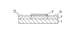
本発明の熱硬化型ダイボンドフィルム(以下、「ダイボンドフィルム」という。)について、ダイシング・ダイボンドフィルムの態様を例にして以下に説明する。本実施の形態に係るダイシング・ダイボンドフィルム10は、ダイシングフィルム上にダイボンドフィルム3が積層された構造である(図1参照)。前記ダイシングフィルムは、基材1上に粘着剤層2が積層された構造である。ダイボンドフィルム3はダイシングフィルムの粘着剤層2上に積層されている。
The thermosetting die-bonding film of the present invention (hereinafter referred to as “die-bonding film”) will be described below by taking an embodiment of a dicing die-bonding film as an example. A dicing die-
本発明のダイボンドフィルム3は、エポキシ樹脂、フェノール樹脂、アクリル共重合体及びフィラーを少なくとも含み構成される。前記ダイボンドフィルム3の80℃〜140℃における熱硬化前の貯蔵弾性率は、10kPa〜10MPaの範囲内であり、好ましくは10kPa〜5MPa、より好ましくは10kPa〜3MPaである。前記貯蔵弾性率を10kPa以上にすることにより、フィルムとしての機械的強度を増し自己支持性を確保することができる。その一方、前記貯蔵弾性率を10MPa以下にすることにより、被着体に対する濡れ性を確保し、接着力の維持が図れる。その結果、ダイボンド後の搬送中に加えられる振動や被着体の湾曲により、半導体チップが被着体から脱落するのを防止することができる。 The die bond film 3 of the present invention includes at least an epoxy resin, a phenol resin, an acrylic copolymer, and a filler. The storage elastic modulus before thermosetting at 80 ° C. to 140 ° C. of the die bond film 3 is in the range of 10 kPa to 10 MPa, preferably 10 kPa to 5 MPa, more preferably 10 kPa to 3 MPa. By setting the storage elastic modulus to 10 kPa or more, the mechanical strength as a film can be increased and the self-supporting property can be ensured. On the other hand, by setting the storage elastic modulus to 10 MPa or less, the wettability with respect to the adherend can be ensured and the adhesive force can be maintained. As a result, it is possible to prevent the semiconductor chip from falling off the adherend due to vibrations applied during conveyance after die bonding or the curvature of the adherend.
また、ダイボンドフィルム3の175℃における熱硬化前の貯蔵弾性率は0.1MPa〜3MPaの範囲内であり、好ましくは0.5kPa〜2.5MPa、より好ましくは0.7kPa〜2.3MPaである。175℃における熱硬化前の貯蔵弾性率を前記数値範囲内にすることにより、半導体チップに対するワイヤーボンディングの際にも十分な接着力を維持させることができる。その結果、ダイボンドフィルム上に接着固定した半導体チップに対してワイヤーボンディングを行う際にも、超音波振動や加熱によるダイボンドフィルムと被着体との接着面でのずり変形を防止し、ワイヤーボンディングの成功率を向上させることができる。 Moreover, the storage elastic modulus before thermosetting of the die-bonding film 3 at 175 ° C. is in the range of 0.1 MPa to 3 MPa, preferably 0.5 kPa to 2.5 MPa, more preferably 0.7 kPa to 2.3 MPa. . By setting the storage elastic modulus before thermosetting at 175 ° C. within the above numerical range, it is possible to maintain a sufficient adhesive force even during wire bonding to a semiconductor chip. As a result, even when wire bonding is performed on a semiconductor chip bonded and fixed on a die bond film, shear deformation on the bonding surface between the die bond film and the adherend due to ultrasonic vibration or heating is prevented, and wire bonding is prevented. The success rate can be improved.
前記ダイボンドフィルム3のガラス転移温度は10℃〜50℃であることが好ましく、20℃〜45℃であることがより好ましい。前記ガラス転移温度が10℃以上にすることにより、半導体チップのダイボンドの際にダイボンドフィルムを構成する接着剤のはみ出しが生じるのを防止することができる。その一方、前記ガラス転移温度を50℃以下にすることにより、被着体に対する濡れ性及び接着性を一層良好に維持することができる。 The glass transition temperature of the die bond film 3 is preferably 10 ° C. to 50 ° C., and more preferably 20 ° C. to 45 ° C. By setting the glass transition temperature to 10 ° C. or higher, it is possible to prevent the adhesive constituting the die bond film from protruding when the semiconductor chip is die bonded. On the other hand, by setting the glass transition temperature to 50 ° C. or lower, the wettability and adhesion to the adherend can be maintained better.
また、エポキシ樹脂とフェノール樹脂の合計重量をX重量部とし、アクリル共重合体の重量をY重量部とした場合に、その配合比率X/Y(−)は0.11〜4が好ましく、0.11〜1.5がより好ましく、0.11〜1.4が更に好ましく、0.11〜1が特に好ましく、0.11〜0.5が一層好ましい。配合比率X/Yを0.11以上にすることにより、175℃で1時間の熱処理を行った後の260℃に於ける貯蔵弾性率を0.1MPa以上にすることができ、耐湿半田リフロー試験においてもダイボンドフィルム3の剥離の発生を防止することができ、信頼性の向上が図れる。その一方、配合比率を4以下にすることにより、ダイボンドフィルム3のフィルムとしての機械的強度を増し、その自己支持性を確保することができる。 Further, when the total weight of the epoxy resin and the phenol resin is X parts by weight and the weight of the acrylic copolymer is Y parts by weight, the blending ratio X / Y (−) is preferably 0.11 to 4, and 0 .11 to 1.5 is more preferable, 0.11 to 1.4 is still more preferable, 0.11 to 1 is particularly preferable, and 0.11 to 0.5 is still more preferable. By setting the blending ratio X / Y to 0.11 or more, the storage elastic modulus at 260 ° C. after heat treatment at 175 ° C. for 1 hour can be made 0.1 MPa or more, and the moisture-resistant solder reflow test Also, the occurrence of peeling of the die bond film 3 can be prevented, and the reliability can be improved. On the other hand, by setting the blending ratio to 4 or less, the mechanical strength of the die bond film 3 as a film can be increased, and the self-supporting property can be secured.
前記エポキシ樹脂は、接着剤組成物として一般に用いられるものであれば特に限定は無く、例えばビスフェノールA型、ビスフェノールF型、ビスフェノールS型、臭素化ビスフェノールA型、水添ビスフェノールA型、ビスフェノールAF型、ビフェニル型、ナフタレン型、フルオンレン型、フェノールノボラック型、オルソクレゾールノボラック型、トリスヒドロキシフェニルメタン型、テトラフェニロールエタン型等の二官能エポキシ樹脂や多官能エポキシ樹脂、又はヒダントイン型、トリスグリシジルイソシアヌレート型若しくはグリシジルアミン型等のエポキシ樹脂が用いられる。これらは単独で、又は2種以上を併用して用いることができる。これらのエポキシ樹脂のうち本発明においては、ベンゼン環、ビフェニル環、ナフタレン環等の芳香族環を有するエポキシ樹脂が特に好ましい。具体的には、例えば、ノボラック型エポキシ樹脂、キシリレン骨格含有フェノールノボラック型エポキシ樹脂、ビフェニル骨格含有ノボラック型エポキシ樹脂、ビスフェノールA型エポキシ樹脂、ビスフェノールF型エポキシ樹脂、テトラメチルビフェノール型エポキシ樹脂、トリフェニルメタン型エポキシ樹脂などが挙げられる。これらのエポキシ樹脂は、硬化剤としてのフェノール樹脂との反応性に富み、耐熱性等に優れるからである。尚、エポキシ樹脂は、半導体素子を腐食させるイオン性不純物等の含有が少ない。 The epoxy resin is not particularly limited as long as it is generally used as an adhesive composition, for example, bisphenol A type, bisphenol F type, bisphenol S type, brominated bisphenol A type, hydrogenated bisphenol A type, bisphenol AF type. Biphenyl type, naphthalene type, fluorene type, phenol novolak type, orthocresol novolak type, trishydroxyphenylmethane type, tetraphenylolethane type, etc., bifunctional epoxy resin or polyfunctional epoxy resin, or hydantoin type, trisglycidyl isocyanurate Type or glycidylamine type epoxy resin is used. These can be used alone or in combination of two or more. Among these epoxy resins, in the present invention, an epoxy resin having an aromatic ring such as a benzene ring, a biphenyl ring, and a naphthalene ring is particularly preferable. Specifically, for example, novolak type epoxy resin, xylylene skeleton-containing phenol novolak type epoxy resin, biphenyl skeleton containing novolak type epoxy resin, bisphenol A type epoxy resin, bisphenol F type epoxy resin, tetramethylbiphenol type epoxy resin, triphenyl Examples include methane type epoxy resins. This is because these epoxy resins are rich in reactivity with a phenol resin as a curing agent and are excellent in heat resistance and the like. The epoxy resin contains little ionic impurities that corrode semiconductor elements.
前記エポキシ樹脂の重量平均分子量が300〜1500の範囲内であることが好ましく、350〜1000の範囲内であることがより好ましい。重量平均分子量が300未満であると、熱硬化後のダイボンドフィルム3の機械的強度、耐熱性、耐湿性が低下する場合がある。その一方、1500より大きいと、熱硬化後のダイボンドフィルムが剛直になって脆弱になる場合がある。尚、本発明に於ける重量平均分子量とは、ゲルパーミエーションクロトマトグラフィー法(GPC)で標準ポリスチレンによる検量線を用いたポリスチレン換算値を意味する。 The weight average molecular weight of the epoxy resin is preferably in the range of 300 to 1500, and more preferably in the range of 350 to 1000. When the weight average molecular weight is less than 300, the mechanical strength, heat resistance, and moisture resistance of the die-bonding film 3 after thermosetting may be lowered. On the other hand, if it is larger than 1500, the die-bonded film after thermosetting may become rigid and brittle. In addition, the weight average molecular weight in this invention means the polystyrene conversion value using the calibration curve by a standard polystyrene by the gel permeation chromatography method (GPC).
更に、前記フェノール樹脂は、前記エポキシ樹脂の硬化剤として作用するものであり、例えば、フェノールノボラック樹脂、フェノールビフェニル樹脂、フェノールアラルキル樹脂、クレゾールノボラック樹脂、tert−ブチルフェノールノボラック樹脂、ノニルフェノールノボラック樹脂等のノボラック型フェノール樹脂、レゾール型フェノール樹脂、ポリパラオキシスチレン等のポリオキシスチレン等が挙げられる。これらは単独で、又は2種以上を併用して用いることができる。これらのフェノール樹脂のうち、下記化学式で表されるビフェニル型フェノールノボラック樹脂や、フェノールアラルキル樹脂が好ましい。半導体装置の接続信頼性を向上させることができるからである。 Further, the phenol resin acts as a curing agent for the epoxy resin. For example, the novolak such as phenol novolak resin, phenol biphenyl resin, phenol aralkyl resin, cresol novolak resin, tert-butylphenol novolak resin, nonylphenol novolak resin, etc. And polyoxystyrene such as polyphenol styrene, resol type phenol resin, and polyparaoxystyrene. These can be used alone or in combination of two or more. Of these phenol resins, biphenyl type phenol novolac resins and phenol aralkyl resins represented by the following chemical formula are preferred. This is because the connection reliability of the semiconductor device can be improved.

尚、前記nは0〜10の自然数であることが好ましく、0〜5の自然数であることがより好ましい。前記数値範囲内にすることにより、ダイボンドフィルム3の流動性の確保が図れる。 The n is preferably a natural number of 0 to 10, and more preferably a natural number of 0 to 5. By making it within the numerical range, the fluidity of the die bond film 3 can be ensured.
前記フェノール樹脂の重量平均分子量が300〜1500の範囲内であることが好ましく、350〜1000の範囲内であることがより好ましい。重量平均分子量が300未満であると、前記エポキシ樹脂の熱硬化が不十分となり十分な強靱性が得られない場合がある。その一方、重量平均分子量が1500より大きいと、高粘度となって、ダイボンドフィルムの作製時の作業性が低下する場合がある。 The weight average molecular weight of the phenol resin is preferably in the range of 300 to 1500, and more preferably in the range of 350 to 1000. When the weight average molecular weight is less than 300, the epoxy resin is not sufficiently cured by heat and sufficient toughness may not be obtained. On the other hand, when the weight average molecular weight is larger than 1500, the viscosity becomes high, and workability at the time of producing the die bond film may be lowered.
前記エポキシ樹脂とフェノール樹脂の配合割合は、例えば、前記エポキシ樹脂成分中のエポキシ基1当量当たりフェノール樹脂中の水酸基が0.5〜2.0当量になるように配合することが好適である。より好適なのは、0.8〜1.2当量である。即ち、両者の配合割合が前記範囲を外れると、十分な硬化反応が進まず、エポキシ樹脂硬化物の特性が劣化し易くなるからである。 The mixing ratio of the epoxy resin and the phenol resin is preferably such that, for example, the hydroxyl group in the phenol resin is 0.5 to 2.0 equivalents per equivalent of epoxy group in the epoxy resin component. More preferred is 0.8 to 1.2 equivalents. That is, if the blending ratio of both is out of the above range, sufficient curing reaction does not proceed and the properties of the cured epoxy resin are likely to deteriorate.
前記アクリル共重合体としては特に限定されないが、本発明においてはカルボキシル基含有アクリル共重合体、エポキシ基含有アクリル共重合体が好ましい。前記カルボキシル基含有アクリル共重合体に用いる官能基モノマーとしてはアクリル酸又はメタクリル酸が挙げられる。アクリル酸又はメタクリル酸の含有量は酸価が1〜4の範囲内となる様に調節される。その残部は、メチルアクリレート、メチルメタクリレートなどの炭素数1〜8のアルキル基を有するアルキルアクリレート、アルキルメタクリレート、スチレン、又はアクリロニトリル等の混合物を用いることができる。これらの中でも、エチル(メタ)アクリレート及び/又はブチル(メタ)アクリレートが特に好ましい。混合比率は、後述する前記アクリル共重合体のガラス転移点(Tg)を考慮して調整することが好ましい。また、重合方法としては特に限定されず、例えば、溶液重合法、隗状重合法、懸濁重合法、乳化重合法等の従来公知の方法を採用することができる。 The acrylic copolymer is not particularly limited, but in the present invention, a carboxyl group-containing acrylic copolymer and an epoxy group-containing acrylic copolymer are preferable. Examples of the functional group monomer used in the carboxyl group-containing acrylic copolymer include acrylic acid and methacrylic acid. The content of acrylic acid or methacrylic acid is adjusted so that the acid value is in the range of 1-4. As the balance, a mixture of alkyl acrylate having 1 to 8 carbon atoms such as methyl acrylate and methyl methacrylate, alkyl methacrylate, styrene, or acrylonitrile can be used. Among these, ethyl (meth) acrylate and / or butyl (meth) acrylate are particularly preferable. The mixing ratio is preferably adjusted in consideration of the glass transition point (Tg) of the acrylic copolymer described later. Moreover, it does not specifically limit as a polymerization method, For example, conventionally well-known methods, such as a solution polymerization method, a cage-like polymerization method, a suspension polymerization method, and an emulsion polymerization method, are employable.
また、前記モノマー成分と共重合可能な他のモノマー成分としては特に限定されず、例えば、アクリロニトリル等が挙げられる。これら共重合可能なモノマー成分の使用量は、全モノマー成分に対し1〜20重量%の範囲内であることが好ましい。当該数値範囲内の他のモノマー成分を含有させることにより、凝集力、接着性などの改質が図れる。 Moreover, it does not specifically limit as another monomer component copolymerizable with the said monomer component, For example, an acrylonitrile etc. are mentioned. These copolymerizable monomer components are preferably used in an amount of 1 to 20% by weight based on the total monomer components. By incorporating other monomer components within the numerical range, modification of cohesive force, adhesiveness, etc. can be achieved.
アクリル共重合体の重合方法としては特に限定されず、例えば、溶液重合法、隗状重合法、懸濁重合法、乳化重合法等の従来公知の方法を採用することができる。 The polymerization method of the acrylic copolymer is not particularly limited, and conventionally known methods such as a solution polymerization method, a cage polymerization method, a suspension polymerization method, and an emulsion polymerization method can be employed.
前記アクリル共重合体のガラス転移点(Tg)は、−30〜30℃であることが好ましく、−20〜15℃であることがより好ましい。ガラス転移点が−30℃以上にすることにより耐熱性が確保され得る。その一方、30℃以下にすることにより、表面状態が粗いウェハにおけるダイシング後のチップ飛びの防止効果が向上する。 The glass transition point (Tg) of the acrylic copolymer is preferably -30 to 30 ° C, and more preferably -20 to 15 ° C. Heat resistance can be ensured by setting the glass transition point to -30 ° C or higher. On the other hand, when the temperature is 30 ° C. or less, the effect of preventing chip jump after dicing in a wafer having a rough surface state is improved.
前記アクリル共重合体の重量平均分子量は、10万〜100万であることが好ましく、35万〜90万であることがより好ましい。重量平均分子量を10万以上にすることにより、被着体表面に対する高温時の接着性に優れ、かつ、耐熱性も向上させることができる。その一方、重量平均分子量を100万以下にすることにより、容易に有機溶剤への溶解することができる。 The weight average molecular weight of the acrylic copolymer is preferably 100,000 to 1,000,000, and more preferably 350,000 to 900,000. By setting the weight average molecular weight to 100,000 or more, it is excellent in adhesiveness at high temperature to the adherend surface, and heat resistance can also be improved. On the other hand, by making the weight average molecular weight 1 million or less, it can be easily dissolved in an organic solvent.
前記フィラーとしては、無機フィラー又は有機フィラーが挙げられる。取り扱い性及び熱伝導性の向上、溶融粘度の調整、並びにチキソトロピック性の付与等の観点からは、無機フィラーが好ましい。 Examples of the filler include inorganic fillers and organic fillers. Inorganic fillers are preferred from the standpoints of improving handleability and thermal conductivity, adjusting melt viscosity, and imparting thixotropic properties.
前記無機フィラーとしては特に限定されず、例えば、シリカ、水酸化アルミニウム、水酸化カルシウム、水酸化マグネシウム、三酸化アンチモン、炭酸カルシウム、炭酸マグネシウム、ケイ酸カルシウム、ケイ酸マグネシウム、酸化カルシウム、酸化マグネシウム、酸化アルミニウム、窒化アルミニウム、ホウ酸アルミニウム、窒化ホウ素、結晶質シリカ、非晶質シリカ等が挙げられる。これらは単独で、又は2種以上を併用して用いることができる。熱伝導性の向上の観点からは、酸化アルミニウム、窒化アルミニウム、窒化ホウ素、結晶性シリカ、非晶質シリカ等が好ましい。また、ダイボンドフィルム3の接着性とのバランスの観点からは、シリカが好ましい。また、前記有機フィラーとしては、ポリイミド、ポリアミドイミド、ポリエーテルエーテルケトン、ポリエーテルイミド、ポリエステルイミド、ナイロン、シリコーン等が挙げられる。これらは単独で、又は2種以上を併用して用いることができる。 The inorganic filler is not particularly limited, for example, silica, aluminum hydroxide, calcium hydroxide, magnesium hydroxide, antimony trioxide, calcium carbonate, magnesium carbonate, calcium silicate, magnesium silicate, calcium oxide, magnesium oxide, Examples thereof include aluminum oxide, aluminum nitride, aluminum borate, boron nitride, crystalline silica, and amorphous silica. These can be used alone or in combination of two or more. From the viewpoint of improving thermal conductivity, aluminum oxide, aluminum nitride, boron nitride, crystalline silica, amorphous silica and the like are preferable. Further, from the viewpoint of balance with the adhesiveness of the die bond film 3, silica is preferable. Examples of the organic filler include polyimide, polyamideimide, polyetheretherketone, polyetherimide, polyesterimide, nylon, and silicone. These can be used alone or in combination of two or more.
前記フィラーの平均粒径は、0.005〜10μmが好ましく、0.05〜1μmがより好ましい。フィラーの平均粒径が0.005μm以上であると、被着体に対する濡れ性を良好なものにし、接着性の低下を抑制することができる。その一方、前記平均粒径を10μm以下にすることにより、フィラーの添加によるダイボンドフィルム3に対する補強効果を高め、耐熱性の向上が図れる。尚、平均粒径が相互に異なるフィラー同士を組み合わせて使用してもよい。また、フィラーの平均粒径は、例えば、光度式の粒度分布計(HORIBA製、装置名;LA−910)により求めた値である。 The average particle diameter of the filler is preferably 0.005 to 10 μm, and more preferably 0.05 to 1 μm. When the average particle size of the filler is 0.005 μm or more, the wettability with respect to the adherend can be improved, and a decrease in adhesiveness can be suppressed. On the other hand, by setting the average particle size to 10 μm or less, the reinforcing effect on the die-bonding film 3 due to the addition of the filler can be enhanced, and the heat resistance can be improved. In addition, you may use it combining the fillers from which an average particle diameter differs mutually. Moreover, the average particle diameter of a filler is the value calculated | required, for example with the photometric type particle size distribution meter (The product made from HORIBA, apparatus name; LA-910).
前記フィラーの形状は特に限定されず、例えば球状、楕円体状のものを使用することができる。 The shape of the filler is not particularly limited, and for example, a spherical or ellipsoidal shape can be used.
また、エポキシ、フェノール樹脂及びアクリル共重合体の合計重量をA重量部とし、フィラーの重量をB重量部とした場合に、比率B/(A+B)は0を超えて0.8以下であることが好ましく、0を超えて7以下であることがより好ましい。前記比率が0であるとフィラー添加による補強効果がなく、ダイボンドフィルム3の耐熱性が低下する傾向がある。その一方、前記比率が0.8を超えると、被着体に対する濡れ性及び接着性が低下する場合がある。 Further, when the total weight of the epoxy, phenol resin and acrylic copolymer is A parts by weight and the weight of the filler is B parts by weight, the ratio B / (A + B) is more than 0 and 0.8 or less. Is more preferable, and more preferably 0 to 7 or less. When the ratio is 0, there is no reinforcing effect due to the filler addition, and the heat resistance of the die bond film 3 tends to decrease. On the other hand, when the ratio exceeds 0.8, wettability and adhesion to the adherend may be deteriorated.
また、ダイボンドフィルム3、3’には、必要に応じて他の添加剤を適宜に配合することができる。他の添加剤としては、例えば難燃剤、シランカップリング剤又はイオントラップ剤等が挙げられる。 In addition, other additives can be appropriately blended in the die bond films 3 and 3 ′ as necessary. Examples of other additives include flame retardants, silane coupling agents, ion trapping agents, and the like.
前記難燃剤としては、例えば、三酸化アンチモン、五酸化アンチモン、臭素化エポキシ樹脂等が挙げられる。これらは、単独で、又は2種以上を併用して用いることができる。 Examples of the flame retardant include antimony trioxide, antimony pentoxide, brominated epoxy resin, and the like. These can be used alone or in combination of two or more.
前記シランカップリング剤としては、例えば、β−(3、4−エポキシシクロヘキシル)エチルトリメトキシシラン、γ−グリシドキシプロピルトリメトキシシラン、γ−グリシドキシプロピルメチルジエトキシシラン等が挙げられる。これらの化合物は、単独で又は2種以上を併用して用いることができる。 Examples of the silane coupling agent include β- (3,4-epoxycyclohexyl) ethyltrimethoxysilane, γ-glycidoxypropyltrimethoxysilane, γ-glycidoxypropylmethyldiethoxysilane, and the like. These compounds can be used alone or in combination of two or more.
前記イオントラップ剤としては、例えばハイドロタルサイト類、水酸化ビスマス等が挙げられる。これらは、単独で又は2種以上を併用して用いることができる。 Examples of the ion trapping agent include hydrotalcites and bismuth hydroxide. These can be used alone or in combination of two or more.
前記エポキシ樹脂とフェノール樹脂の熱硬化促進触媒としては特に限定されず、例えば、トリフェニルフォスフィン骨格、アミン骨格、トリフェニルボラン骨格、トリハロゲンボラン骨格等の何れかからなる塩が好ましい。 The thermosetting acceleration catalyst for the epoxy resin and the phenol resin is not particularly limited, and for example, a salt composed of any one of a triphenylphosphine skeleton, an amine skeleton, a triphenylborane skeleton, a trihalogenborane skeleton, and the like is preferable.
ダイボンドフィルム3の厚さ(積層体の場合は、総厚)は特に限定されないが、例えば、5〜100μm程度、好ましくは5〜50μm程度である。 Although the thickness (in the case of a laminated body) of the die-bonding film 3 is not specifically limited, For example, it is about 5-100 micrometers, Preferably it is about 5-50 micrometers.
尚、ダイボンドフィルムは、例えば接着剤層の単層のみからなる構成とすることができる。また、ガラス転移温度の異なる熱可塑性樹脂、熱硬化温度の異なる熱硬化性樹脂を適宜に組み合わせて、2層以上の多層構造にしてもよい。尚、半導体ウェハのダイシング工程では切削水を使用することから、ダイボンドフィルムが吸湿して、常態以上の含水率になる場合がある。この様な高含水率のまま、基板等に接着させると、アフターキュアの段階で接着界面に水蒸気が溜まり、浮きが発生する場合がある。従って、ダイボンドフィルムとしては、透湿性の高いコア材料を接着剤層で挟んだ構成とすることにより、アフターキュアの段階では、水蒸気がフィルムを通じて拡散して、かかる問題を回避することが可能となる。かかる観点から、ダイボンドフィルムはコア材料の片面又は両面に接着剤層を形成した多層構造にしてもよい。 In addition, a die-bonding film can be made into the structure which consists only of a single layer of an adhesive bond layer, for example. Alternatively, a thermoplastic resin having a different glass transition temperature and a thermosetting resin having a different thermosetting temperature may be appropriately combined to form a multilayer structure having two or more layers. In addition, since cutting water is used in the dicing process of the semiconductor wafer, the die-bonding film may absorb moisture and have a moisture content higher than that of the normal state. When bonded to a substrate or the like with such a high water content, water vapor may accumulate at the bonding interface at the stage of after-curing and float may occur. Therefore, the die bond film has a structure in which a core material having high moisture permeability is sandwiched between adhesive layers, so that water vapor diffuses through the film at the after-curing stage, and this problem can be avoided. . From this viewpoint, the die bond film may have a multilayer structure in which an adhesive layer is formed on one side or both sides of the core material.
前記コア材料としては、フィルム(例えばポリイミドフィルム、ポリエステルフィルム、ポリエチレンテレフタレートフィルム、ポリエチレンナフタレートフィルム、ポリカーボネートフィルム等)、ガラス繊維やプラスチック製不織繊維で強化された樹脂基板、ミラーシリコンウェハ、シリコン基板又はガラス基板等が挙げられる。 Examples of the core material include films (for example, polyimide films, polyester films, polyethylene terephthalate films, polyethylene naphthalate films, polycarbonate films), resin substrates reinforced with glass fibers and plastic non-woven fibers, mirror silicon wafers, silicon substrates Or a glass substrate etc. are mentioned.
また、ダイボンドフィルム3は、セパレータにより保護されていることが好ましい(図示せず)。セパレータは、実用に供するまでダイボンドフィルムを保護する保護材としての機能を有している。また、セパレータは、更に、ダイシングフィルムにダイボンドフィルム3、3’を転写する際の支持基材として用いることができる。セパレータはダイボンドフィルム上にワークを貼着する際に剥がされる。セパレータとしては、ポリエチレンテレフタレート(PET)、ポリエチレン、ポリプロピレンや、フッ素系剥離剤、長鎖アルキルアクリレート系剥離剤等の剥離剤により表面コートされたプラスチックフィルムや紙等も使用可能である。 The die bond film 3 is preferably protected by a separator (not shown). The separator has a function as a protective material for protecting the die bond film until it is put into practical use. Further, the separator can be used as a supporting substrate when transferring the die bond films 3 and 3 ′ to the dicing film. The separator is peeled off when the workpiece is stuck on the die bond film. As the separator, a plastic film or paper surface-coated with a release agent such as polyethylene terephthalate (PET), polyethylene, polypropylene, a fluorine release agent, or a long-chain alkyl acrylate release agent can be used.
尚、本発明に係るダイシング・ダイボンドフィルムとしては、図1に示すダイボンドフィルム3の他に、図2に示す様に半導体ウェハ貼り付け部分にのみダイボンドフィルム3’を積層したダイシング・ダイボンドフィルム11の構成であってもよい。
As the dicing die-bonding film according to the present invention, in addition to the die-bonding film 3 shown in FIG. 1, as shown in FIG. 2, a dicing die-
前記基材1はダイシング・ダイボンドフィルム10、11の強度母体となるものである。例えば、低密度ポリエチレン、直鎖状ポリエチレン、中密度ポリエチレン、高密度ポリエチレン、超低密度ポリエチレン、ランダム共重合ポリプロピレン、ブロック共重合ポリプロピレン、ホモポリプロレン、ポリブテン、ポリメチルペンテン等のポリオレフィン、エチレン−酢酸ビニル共重合体、アイオノマー樹脂、エチレン−(メタ)アクリル酸共重合体、エチレン−(メタ)アクリル酸エステル(ランダム、交互)共重合体、エチレン−ブテン共重合体、エチレン−ヘキセン共重合体、ポリウレタン、ポリエチレンテレフタレート、ポリエチレンナフタレート等のポリエステル、ポリカーボネート、ポリイミド、ポリエーテルエーテルケトン、ポリイミド、ポリエーテルイミド、ポリアミド、全芳香族ポリアミド、ポリフェニルスルフイド、アラミド(紙)、ガラス、ガラスクロス、フッ素樹脂、ポリ塩化ビニル、ポリ塩化ビニリデン、セルロース系樹脂、シリコーン樹脂、金属(箔)、紙等が挙げられる。粘着剤層2が紫外線硬化型である場合、基材1は紫外線に対し透過性を有するものが好ましい。
The substrate 1 serves as a strength matrix for the dicing die-
また基材1の材料としては、前記樹脂の架橋体等のポリマーが挙げられる。前記プラスチックフィルムは、無延伸で用いてもよく、必要に応じて一軸又は二軸の延伸処理を施したものを用いてもよい。延伸処理等により熱収縮性を付与した樹脂シートによれば、ダイシング後にその基材1を熱収縮させることにより粘着剤層2とダイボンドフィルム3、3’との接着面積を低下させて、半導体チップの回収の容易化を図ることができる。
Moreover, as a material of the base material 1, polymers, such as the crosslinked body of the said resin, are mentioned. The plastic film may be used unstretched or may be uniaxially or biaxially stretched as necessary. According to the resin sheet to which heat shrinkability is imparted by stretching treatment or the like, the adhesive area between the pressure-
基材1の表面は、隣接する層との密着性、保持性等を高める為、慣用の表面処理、例えば、クロム酸処理、オゾン暴露、火炎暴露、高圧電撃暴露、イオン化放射線処理等の化学的又は物理的処理、下塗剤(例えば、後述する粘着物質)によるコーティング処理を施すことができる。 The surface of the substrate 1 is chemically treated by conventional surface treatments such as chromic acid treatment, ozone exposure, flame exposure, high piezoelectric impact exposure, ionizing radiation treatment, etc. in order to improve adhesion and retention with adjacent layers. Alternatively, a physical treatment or a coating treatment with a primer (for example, an adhesive substance described later) can be performed.
前記基材1は、同種又は異種のものを適宜に選択して使用することができ、必要に応じて数種をブレンドしたものを用いることができる。また、基材1には、帯電防止能を付与する為、前記の基材1上に金属、合金、これらの酸化物等からなる厚さが30〜500Å程度の導電性物質の蒸着層を設けることができる。基材1は単層又は2種以上の複層でもよい。 The base material 1 can be used by appropriately selecting the same kind or different kinds, and a blend of several kinds can be used as necessary. Further, in order to impart antistatic ability to the base material 1, a conductive material vapor deposition layer having a thickness of about 30 to 500 mm made of metal, alloy, oxides thereof, or the like is provided on the base material 1. be able to. The substrate 1 may be a single layer or two or more layers.
基材1の厚さは、特に制限されず適宜に決定できるが、一般的には5〜200μm程度である。 The thickness of the substrate 1 is not particularly limited and can be appropriately determined, but is generally about 5 to 200 μm.
前記粘着剤層2は紫外線硬化型粘着剤を含み構成されている。紫外線硬化型粘着剤は、紫外線の照射により架橋度を増大させてその粘着力を容易に低下させることができ、図2に示す粘着剤層2の半導体ウェハ貼り付け部分に対応する部分2aのみを紫外線照射することにより他の部分2bとの粘着力の差を設けることができる。
The pressure-
また、図2に示すダイボンドフィルム3’に合わせて紫外線硬化型の粘着剤層2を硬化させることにより、粘着力が著しく低下した前記部分2aを容易に形成できる。硬化し、粘着力の低下した前記部分2aにダイボンドフィルム3’が貼付けられる為、粘着剤層2の前記部分2aとダイボンドフィルム3’との界面は、ピックアップ時に容易に剥がれる性質を有する。一方、紫外線を照射していない部分は十分な粘着力を有しており、前記部分2bを形成する。
Further, by curing the ultraviolet curable pressure-
前述の通り、図1に示すダイシング・ダイボンドフィルム10の粘着剤層2に於いて、未硬化の紫外線硬化型粘着剤により形成されている前記部分2bはダイボンドフィルム3と粘着し、ダイシングする際の保持力を確保できる。この様に紫外線硬化型粘着剤は、半導体チップを被着体に固着する為のダイボンドフィルム3を、接着・剥離のバランスよく支持することができる。図2に示すダイシング・ダイボンドフィルム11の粘着剤層2に於いては、前記部分2bがウェハリング16を固定することができる。前記被着体6としては特に限定されず、例えば、BGA基板等の各種基板、リードフレーム、半導体素子、スペーサ等が挙げられる。
As described above, in the pressure-
前記紫外線硬化型粘着剤は、炭素−炭素二重結合等の紫外線硬化性の官能基を有し、かつ粘着性を示すものを特に制限なく使用することができる。紫外線硬化型粘着剤としては、例えば、アクリル系粘着剤、ゴム系粘着剤等の一般的な感圧性粘着剤に、紫外線硬化性のモノマー成分やオリゴマー成分を配合した添加型の紫外線硬化型粘着剤を例示できる。 As the ultraviolet curable pressure-sensitive adhesive, those having an ultraviolet curable functional group such as a carbon-carbon double bond and exhibiting adhesiveness can be used without particular limitation. Examples of the ultraviolet curable pressure-sensitive adhesive include an additive-type ultraviolet curable pressure-sensitive adhesive in which an ultraviolet curable monomer component or an oligomer component is blended with a general pressure-sensitive adhesive such as an acrylic pressure-sensitive adhesive or a rubber-based pressure-sensitive adhesive. Can be illustrated.
前記感圧性粘着剤としては、半導体ウェハやガラス等の汚染をきらう電子部品の超純水やアルコール等の有機溶剤による清浄洗浄性等の点から、アクリル系ポリマーをベースポリマーとするアクリル系粘着剤が好ましい。 The pressure-sensitive adhesive is an acrylic pressure-sensitive adhesive based on an acrylic polymer from the standpoint of cleanability with an organic solvent such as ultrapure water or alcohol for electronic components that are difficult to contaminate semiconductor wafers and glass. Is preferred.
前記アクリル系ポリマーとしては、例えば、(メタ)アクリル酸アルキルエステル(例えば、メチルエステル、エチルエステル、プロピルエステル、イソプロピルエステル、ブチルエステル、イソブチルエステル、s−ブチルエステル、t−ブチルエステル、ペンチルエステル、イソペンチルエステル、ヘキシルエステル、ヘプチルエステル、オクチルエステル、2−エチルヘキシルエステル、イソオクチルエステル、ノニルエステル、デシルエステル、イソデシルエステル、ウンデシルエステル、ドデシルエステル、トリデシルエステル、テトラデシルエステル、ヘキサデシルエステル、オクタデシルエステル、エイコシルエステル等のアルキル基の炭素数1〜30、特に炭素数4〜18の直鎖状又は分岐鎖状のアルキルエステル等)及び(メタ)アクリル酸シクロアルキルエステル(例えば、シクロペンチルエステル、シクロヘキシルエステル等)の1種又は2種以上を単量体成分として用いたアクリル系ポリマー等が挙げられる。尚、(メタ)アクリル酸エステルとはアクリル酸エステル及び/又はメタクリル酸エステルをいい、本発明の(メタ)とは全て同様の意味である。 Examples of the acrylic polymer include (meth) acrylic acid alkyl esters (for example, methyl ester, ethyl ester, propyl ester, isopropyl ester, butyl ester, isobutyl ester, s-butyl ester, t-butyl ester, pentyl ester, Isopentyl ester, hexyl ester, heptyl ester, octyl ester, 2-ethylhexyl ester, isooctyl ester, nonyl ester, decyl ester, isodecyl ester, undecyl ester, dodecyl ester, tridecyl ester, tetradecyl ester, hexadecyl ester , Octadecyl esters, eicosyl esters, etc., alkyl groups having 1 to 30 carbon atoms, especially 4 to 18 carbon linear or branched alkyl esters, etc.) and Meth) acrylic acid cycloalkyl esters (e.g., cyclopentyl ester, acrylic polymers such as one or more was used as a monomer component of the cyclohexyl ester etc.). In addition, (meth) acrylic acid ester means acrylic acid ester and / or methacrylic acid ester, and (meth) of the present invention has the same meaning.
前記アクリル系ポリマーは、凝集力、耐熱性等の改質を目的として、必要に応じ、前記(メタ)アクリル酸アルキルエステル又はシクロアルキルエステルと共重合可能な他のモノマー成分に対応する単位を含んでいてもよい。この様なモノマー成分として、例えば、アクリル酸、メタクリル酸、カルボキシエチル(メタ)アクリレート、カルボキシペンチル(メタ)アクリレート、イタコン酸、マレイン酸、フマル酸、クロトン酸等のカルボキシル基含有モノマー;無水マレイン酸、無水イタコン酸等の酸無水物モノマー;(メタ)アクリル酸2−ヒドロキシエチル、(メタ)アクリル酸2−ヒドロキシプロピル、(メタ)アクリル酸4−ヒドロキシブチル、(メタ)アクリル酸6−ヒドロキシヘキシル、(メタ)アクリル酸8−ヒドロキシオクチル、(メタ)アクリル酸10−ヒドロキシデシル、(メタ)アクリル酸12−ヒドロキシラウリル、(4−ヒドロキシメチルシクロヘキシル)メチル(メタ)アクリレート等のヒドロキシル基含有モノマー;スチレンスルホン酸、アリルスルホン酸、2−(メタ)アクリルアミド−2−メチルプロパンスルホン酸、(メタ)アクリルアミドプロパンスルホン酸、スルホプロピル(メタ)アクリレート、(メタ)アクリロイルオキシナフタレンスルホン酸等のスルホン酸基含有モノマー;2−ヒドロキシエチルアクリロイルホスフェート等のリン酸基含有モノマー;アクリルアミド、アクリロニトリル等が挙げられる。これら共重合可能なモノマー成分は、1種又は2種以上使用できる。これら共重合可能なモノマーの使用量は、全モノマー成分の40重量%以下が好ましい。 The acrylic polymer contains units corresponding to other monomer components copolymerizable with the (meth) acrylic acid alkyl ester or cycloalkyl ester, if necessary, for the purpose of modifying cohesive force, heat resistance and the like. You may go out. Examples of such monomer components include, for example, carboxyl group-containing monomers such as acrylic acid, methacrylic acid, carboxyethyl (meth) acrylate, carboxypentyl (meth) acrylate, itaconic acid, maleic acid, fumaric acid, and crotonic acid; maleic anhydride Acid anhydride monomers such as itaconic anhydride; 2-hydroxyethyl (meth) acrylate, 2-hydroxypropyl (meth) acrylate, 4-hydroxybutyl (meth) acrylate, 6-hydroxyhexyl (meth) acrylate Hydroxyl group-containing monomers such as 8-hydroxyoctyl (meth) acrylate, 10-hydroxydecyl (meth) acrylate, 12-hydroxylauryl (meth) acrylate, (4-hydroxymethylcyclohexyl) methyl (meth) acrylate; Styrene Contains sulfonic acid groups such as phonic acid, allylsulfonic acid, 2- (meth) acrylamide-2-methylpropanesulfonic acid, (meth) acrylamidepropanesulfonic acid, sulfopropyl (meth) acrylate, (meth) acryloyloxynaphthalenesulfonic acid Monomers; Phosphoric acid group-containing monomers such as 2-hydroxyethyl acryloyl phosphate; acrylamide, acrylonitrile and the like. One or more of these copolymerizable monomer components can be used. The amount of these copolymerizable monomers used is preferably 40% by weight or less based on the total monomer components.
更に、前記アクリル系ポリマーは、架橋させる為、多官能性モノマー等も、必要に応じて共重合用モノマー成分として含むことができる。この様な多官能性モノマーとして、例えば、ヘキサンジオールジ(メタ)アクリレート、(ポリ)エチレングリコールジ(メタ)アクリレート、(ポリ)プロピレングリコールジ(メタ)アクリレート、ネオペンチルグリコールジ(メタ)アクリレート、ペンタエリスリトールジ(メタ)アクリレート、トリメチロールプロパントリ(メタ)アクリレート、ペンタエリスリトールトリ(メタ)アクリレート、ジペンタエリスリトールヘキサ(メタ)アクリレート、エポキシ(メタ)アクリレート、ポリエステル(メタ)アクリレート、ウレタン(メタ)アクリレート等が挙げられる。これらの多官能性モノマーも1種又は2種以上用いることができる。多官能性モノマーの使用量は、粘着特性等の点から、全モノマー成分の30重量%以下が好ましい。 Furthermore, since the acrylic polymer is crosslinked, a polyfunctional monomer or the like can be included as a monomer component for copolymerization, if necessary. Examples of such polyfunctional monomers include hexanediol di (meth) acrylate, (poly) ethylene glycol di (meth) acrylate, (poly) propylene glycol di (meth) acrylate, neopentyl glycol di (meth) acrylate, Pentaerythritol di (meth) acrylate, trimethylolpropane tri (meth) acrylate, pentaerythritol tri (meth) acrylate, dipentaerythritol hexa (meth) acrylate, epoxy (meth) acrylate, polyester (meth) acrylate, urethane (meth) An acrylate etc. are mentioned. These polyfunctional monomers can also be used alone or in combination of two or more. The amount of the polyfunctional monomer used is preferably 30% by weight or less of the total monomer components from the viewpoint of adhesive properties and the like.
前記アクリル系ポリマーは、単一モノマー又は2種以上のモノマー混合物を重合に付すことにより得られる。重合は、溶液重合、乳化重合、塊状重合、懸濁重合等の何れの方式で行うこともできる。清浄な被着体への汚染防止等の点から、低分子量物質の含有量が小さいのが好ましい。この点から、アクリル系ポリマーの数平均分子量は、好ましくは30万以上、更に好ましくは40万〜300万程度である。 The acrylic polymer can be obtained by subjecting a single monomer or a mixture of two or more monomers to polymerization. The polymerization can be performed by any method such as solution polymerization, emulsion polymerization, bulk polymerization, suspension polymerization and the like. From the viewpoint of preventing contamination of a clean adherend, the content of the low molecular weight substance is preferably small. From this point, the number average molecular weight of the acrylic polymer is preferably 300,000 or more, more preferably about 400,000 to 3,000,000.
また、前記粘着剤には、ベースポリマーであるアクリル系ポリマー等の数平均分子量を高める為、外部架橋剤を適宜に採用することもできる。外部架橋方法の具体的手段としては、ポリイソシアネート化合物、エポキシ化合物、アジリジン化合物、メラミン系架橋剤等のいわゆる架橋剤を添加し反応させる方法が挙げられる。外部架橋剤を使用する場合、その使用量は、架橋すべきベースポリマーとのバランスにより、更には、粘着剤としての使用用途によって適宜決定される。一般的には、前記ベースポリマー100重量部に対して、5重量部程度以下、更には0.1〜5重量部配合するのが好ましい。更に、粘着剤には、必要により、前記成分のほかに、従来公知の各種の粘着付与剤、老化防止剤等の添加剤を用いてもよい。 In addition, an external cross-linking agent can be appropriately employed for the pressure-sensitive adhesive in order to increase the number average molecular weight of an acrylic polymer as a base polymer. Specific examples of the external crosslinking method include a method of adding a so-called crosslinking agent such as a polyisocyanate compound, an epoxy compound, an aziridine compound, a melamine crosslinking agent, and reacting them. When using an external cross-linking agent, the amount used is appropriately determined depending on the balance with the base polymer to be cross-linked and further depending on the intended use as an adhesive. Generally, it is preferable to add about 5 parts by weight or less, and further 0.1 to 5 parts by weight with respect to 100 parts by weight of the base polymer. Furthermore, you may use additives, such as conventionally well-known various tackifier and anti-aging agent, other than the said component as needed to an adhesive.
配合する前記紫外線硬化性のモノマー成分としては、例えば、ウレタンオリゴマー、ウレタン(メタ)アクリレート、トリメチロールプロパントリ(メタ)アクリレート、テトラメチロールメタンテトラ(メタ)アクリレート、ペンタエリスリトールトリ(メタ)アクリレート、ペンタエリストールテトラ(メタ)アクリレート、ジペンタエリストールモノヒドロキシペンタ(メタ)アクリレート、ジペンタエリスリトールヘキサ(メタ)アクリレート、1,4−ブタンジオールジ(メタ)アクリレート等が挙げられる。また紫外線硬化性のオリゴマー成分はウレタン系、ポリエーテル系、ポリエステル系、ポリカーボネート系、ポリブタジエン系等種々のオリゴマーがあげられ、その分子量が100〜30000程度の範囲のものが適当である。紫外線硬化性のモノマー成分やオリゴマー成分の配合量は、前記粘着剤層の種類に応じて、粘着剤層の粘着力を低下できる量を、適宜に決定することができる。一般的には、粘着剤を構成するアクリル系ポリマー等のベースポリマー100重量部に対して、例えば5〜500重量部、好ましくは40〜150重量部程度である。 Examples of the ultraviolet curable monomer component to be blended include urethane oligomer, urethane (meth) acrylate, trimethylolpropane tri (meth) acrylate, tetramethylolmethanetetra (meth) acrylate, pentaerythritol tri (meth) acrylate, and penta. Examples include erythritol tetra (meth) acrylate, dipentaerythritol monohydroxypenta (meth) acrylate, dipentaerythritol hexa (meth) acrylate, 1,4-butanediol di (meth) acrylate, and the like. Examples of the ultraviolet curable oligomer component include urethane, polyether, polyester, polycarbonate, and polybutadiene oligomers, and those having a molecular weight in the range of about 100 to 30000 are suitable. The blending amount of the ultraviolet curable monomer component and oligomer component can be appropriately determined in accordance with the type of the pressure-sensitive adhesive layer, and the amount capable of reducing the pressure-sensitive adhesive strength of the pressure-sensitive adhesive layer. Generally, the amount is, for example, about 5 to 500 parts by weight, preferably about 40 to 150 parts by weight with respect to 100 parts by weight of the base polymer such as an acrylic polymer constituting the pressure-sensitive adhesive.
また、紫外線硬化型粘着剤としては、前記説明した添加型の紫外線硬化型粘着剤のほかに、ベースポリマーとして、炭素−炭素二重結合をポリマー側鎖又は主鎖中もしくは主鎖末端に有するものを用いた内在型の紫外線硬化型粘着剤が挙げられる。内在型の紫外線硬化型粘着剤は、低分子量成分であるオリゴマー成分等を含有する必要がなく、又は多くは含まない為、経時的にオリゴマー成分等が粘着剤中を移動することなく、安定した層構造の粘着剤層を形成することができる為好ましい。 In addition to the additive-type UV-curable pressure-sensitive adhesive described above, the UV-curable pressure-sensitive adhesive has a carbon-carbon double bond in the polymer side chain, main chain, or main chain terminal as a base polymer. Intrinsic ultraviolet curable pressure sensitive adhesives using Intrinsic UV curable pressure-sensitive adhesive does not need to contain an oligomer component or the like, which is a low molecular weight component, or does not contain much, so that the oligomer component or the like does not move through the pressure-sensitive adhesive over time and is stable. It is preferable because an adhesive layer having a layer structure can be formed.
前記炭素−炭素二重結合を有するベースポリマーは、炭素−炭素二重結合を有し、かつ粘着性を有するものを特に制限なく使用できる。この様なベースポリマーとしては、アクリル系ポリマーを基本骨格とするものが好ましい。アクリル系ポリマーの基本骨格としては、前記例示したアクリル系ポリマーが挙げられる。 As the base polymer having a carbon-carbon double bond, those having a carbon-carbon double bond and having adhesiveness can be used without particular limitation. As such a base polymer, those having an acrylic polymer as a basic skeleton are preferable. Examples of the basic skeleton of the acrylic polymer include the acrylic polymers exemplified above.
前記アクリル系ポリマーへの炭素−炭素二重結合の導入法は特に制限されず、様々な方法を採用できるが、炭素−炭素二重結合はポリマー側鎖に導入するのが分子設計において容易である。例えば、予め、アクリル系ポリマーに官能基を有するモノマーを共重合した後、この官能基と反応しうる官能基及び炭素−炭素二重結合を有する化合物を、炭素−炭素二重結合の紫外線硬化性を維持したまま縮合又は付加反応させる方法が挙げられる。 The method for introducing a carbon-carbon double bond into the acrylic polymer is not particularly limited, and various methods can be adopted. However, it is easy in molecular design to introduce a carbon-carbon double bond into a polymer side chain. . For example, after a monomer having a functional group is previously copolymerized with an acrylic polymer, a compound having a functional group capable of reacting with the functional group and a carbon-carbon double bond is converted into an ultraviolet curable carbon-carbon double bond. A method of performing condensation or addition reaction while maintaining the above.
これら官能基の組合せの例としては、カルボン酸基とエポキシ基、カルボン酸基とアジリジル基、ヒドロキシル基とイソシアネート基等が挙げられる。これら官能基の組合せのなかでも反応追跡の容易さから、ヒドロキシル基とイソシアネート基との組合せが好適である。また、これら官能基の組み合わせにより、前記炭素−炭素二重結合を有するアクリル系ポリマーを生成するような組合せであれば、官能基はアクリル系ポリマーと前記化合物のいずれの側にあってもよいが、前記の好ましい組み合わせでは、アクリル系ポリマーがヒドロキシル基を有し、前記化合物がイソシアネート基を有する場合が好適である。この場合、炭素−炭素二重結合を有するイソシアネート化合物としては、例えば、メタクリロイルイソシアネート、2−メタクリロイルオキシエチルイソシアネート、m−イソプロペニル−α,α−ジメチルベンジルイソシアネート等が挙げられる。また、アクリル系ポリマーとしては、前記例示のヒドロキシ基含有モノマーや2−ヒドロキシエチルビニルエーテル、4−ヒドロキシブチルビニルエーテル、ジエチレングルコールモノビニルエーテルのエーテル系化合物等を共重合したものが用いられる。 Examples of combinations of these functional groups include carboxylic acid groups and epoxy groups, carboxylic acid groups and aziridyl groups, hydroxyl groups and isocyanate groups, and the like. Among these combinations of functional groups, a combination of a hydroxyl group and an isocyanate group is preferable because of easy tracking of the reaction. Moreover, the functional group may be on either side of the acrylic polymer and the compound as long as the acrylic polymer having the carbon-carbon double bond is generated by a combination of these functional groups. In the preferable combination, it is preferable that the acrylic polymer has a hydroxyl group and the compound has an isocyanate group. In this case, examples of the isocyanate compound having a carbon-carbon double bond include methacryloyl isocyanate, 2-methacryloyloxyethyl isocyanate, m-isopropenyl-α, α-dimethylbenzyl isocyanate, and the like. Further, as the acrylic polymer, those obtained by copolymerizing the above-exemplified hydroxy group-containing monomers, ether compounds of 2-hydroxyethyl vinyl ether, 4-hydroxybutyl vinyl ether, diethylene glycol monovinyl ether, or the like are used.
前記内在型の紫外線硬化型粘着剤は、前記炭素−炭素二重結合を有するベースポリマー(特にアクリル系ポリマー)を単独で使用することができるが、特性を悪化させない程度に前記紫外線硬化性のモノマー成分やオリゴマー成分を配合することもできる。紫外線硬化性のオリゴマー成分等は、通常ベースポリマー100重量部に対して30重量部の範囲内であり、好ましくは0〜10重量部の範囲である。 As the intrinsic ultraviolet curable pressure-sensitive adhesive, the base polymer (particularly acrylic polymer) having the carbon-carbon double bond can be used alone, but the ultraviolet curable monomer does not deteriorate the characteristics. Components and oligomer components can also be blended. The UV-curable oligomer component or the like is usually in the range of 30 parts by weight, preferably in the range of 0 to 10 parts by weight with respect to 100 parts by weight of the base polymer.
前記紫外線硬化型粘着剤には、紫外線等により硬化させる場合には光重合開始剤を含有させる。光重合開始剤としては、例えば、4−(2−ヒドロキシエトキシ)フェニル(2−ヒドロキシ−2−プロピル)ケトン、α−ヒドロキシ−α,α’−ジメチルアセトフェノン、2−メチル−2−ヒドロキシプロピオフェノン、1−ヒドロキシシクロヘキシルフェニルケトン等のα−ケトール系化合物;メトキシアセトフェノン、2,2−ジメトキシ−2−フェニルアセトフェノン、2,2−ジエトキシアセトフェノン、2−メチル−1−[4−(メチルチオ)−フェニル]−2−モルホリノプロパン−1等のアセトフェノン系化合物;ベンゾインエチルエーテル、ベンゾインイソプロピルエーテル、アニソインメチルエーテル等のベンゾインエーテル系化合物;ベンジルジメチルケタール等のケタール系化合物;2−ナフタレンスルホニルクロリド等の芳香族スルホニルクロリド系化合物;1−フェノン−1,1―プロパンジオン−2−(o−エトキシカルボニル)オキシム等の光活性オキシム系化合物;ベンゾフェノン、ベンゾイル安息香酸、3,3’−ジメチル−4−メトキシベンゾフェノン等のベンゾフェノン系化合物;チオキサンソン、2−クロロチオキサンソン、2−メチルチオキサンソン、2,4−ジメチルチオキサンソン、イソプロピルチオキサンソン、2,4−ジクロロチオキサンソン、2,4−ジエチルチオキサンソン、2,4−ジイソプロピルチオキサンソン等のチオキサンソン系化合物;カンファーキノン;ハロゲン化ケトン;アシルホスフィノキシド;アシルホスフォナート等が挙げられる。光重合開始剤の配合量は、粘着剤を構成するアクリル系ポリマー等のベースポリマー100重量部に対して、例えば0.05〜20重量部程度である。 The ultraviolet curable pressure-sensitive adhesive contains a photopolymerization initiator when cured by ultraviolet rays or the like. Examples of the photopolymerization initiator include 4- (2-hydroxyethoxy) phenyl (2-hydroxy-2-propyl) ketone, α-hydroxy-α, α′-dimethylacetophenone, 2-methyl-2-hydroxypropio Α-ketol compounds such as phenone and 1-hydroxycyclohexyl phenyl ketone; methoxyacetophenone, 2,2-dimethoxy-2-phenylacetophenone, 2,2-diethoxyacetophenone, 2-methyl-1- [4- (methylthio) Acetophenone compounds such as -phenyl] -2-morpholinopropane-1; benzoin ether compounds such as benzoin ethyl ether, benzoin isopropyl ether and anisoin methyl ether; ketal compounds such as benzyldimethyl ketal; 2-naphthalenesulfonyl chloride Aromatic sulfonyl chloride compounds such as 1; photoactive oxime compounds such as 1-phenone-1,1-propanedione-2- (o-ethoxycarbonyl) oxime; benzophenone, benzoylbenzoic acid, 3,3′-dimethyl Benzophenone compounds such as -4-methoxybenzophenone; thioxanthone, 2-chlorothioxanthone, 2-methylthioxanthone, 2,4-dimethylthioxanthone, isopropylthioxanthone, 2,4-dichlorothioxanthone, 2 Thioxanthone compounds such as 1,4-diethylthioxanthone and 2,4-diisopropylthioxanthone; camphorquinone; halogenated ketone; acyl phosphinoxide; acyl phosphonate. The compounding quantity of a photoinitiator is about 0.05-20 weight part with respect to 100 weight part of base polymers, such as an acryl-type polymer which comprises an adhesive.
また紫外線硬化型粘着剤としては、例えば、特開昭60−196956号公報に開示されている、不飽和結合を2個以上有する付加重合性化合物、エポキシ基を有するアルコキシシラン等の光重合性化合物と、カルボニル化合物、有機硫黄化合物、過酸化物、アミン、オニウム塩系化合物等の光重合開始剤とを含有するゴム系粘着剤やアクリル系粘着剤等が挙げられる。 Examples of the ultraviolet curable pressure-sensitive adhesive include photopolymerizable compounds such as addition polymerizable compounds having two or more unsaturated bonds and alkoxysilanes having an epoxy group disclosed in JP-A-60-196956. And a rubber-based pressure-sensitive adhesive and an acrylic pressure-sensitive adhesive containing a photopolymerization initiator such as a carbonyl compound, an organic sulfur compound, a peroxide, an amine, and an onium salt-based compound.
前記粘着剤層2に前記部分2aを形成する方法としては、基材1に紫外線硬化型の粘着剤層2を形成した後、前記部分2aに部分的に紫外線を照射し硬化させる方法が挙げられる。部分的な紫外線照射は、半導体ウェハ貼り付け部分3a以外の部分3b等に対応するパターンを形成したフォトマスクを介して行うことができる。また、スポット的に紫外線を照射し硬化させる方法等が挙げられる。紫外線硬化型の粘着剤層2の形成は、セパレータ上に設けたものを基材1上に転写することにより行うことができる。部分的な紫外線硬化はセパレータ上に設けた紫外線硬化型の粘着剤層2に行うこともできる。
Examples of the method for forming the
ダイシング・ダイボンドフィルム10の粘着剤層2に於いては、前記部分2aの粘着力<その他の部分2bの粘着力、となるように粘着剤層2の一部を紫外線照射してもよい。即ち、基材1の少なくとも片面の、半導体ウェハ貼り付け部分3aに対応する部分以外の部分の全部又は一部が遮光されたものを用い、これに紫外線硬化型の粘着剤層2を形成した後に紫外線照射して、半導体ウェハ貼り付け部分3aに対応する部分を硬化させ、粘着力を低下させた前記部分2aを形成することができる。遮光材料としては、支持フィルム上でフォトマスクになりえるものを印刷や蒸着等で作製することができる。これにより、効率よく本発明のダイシング・ダイボンドフィルム10を製造可能である。
In the pressure-
尚、紫外線照射の際に、酸素による硬化阻害が起こる場合は、紫外線硬化型の粘着剤層2の表面から酸素(空気)を遮断するのが望ましい。その方法としては、例えば粘着剤層2の表面をセパレータで被覆する方法や、窒素ガス雰囲気中で紫外線等の紫外線の照射を行う方法等が挙げられる。
In the case where curing inhibition by oxygen occurs during ultraviolet irradiation, it is desirable to block oxygen (air) from the surface of the ultraviolet curable pressure-
粘着剤層2の厚さは、特に限定されないが、チップ切断面の欠け防止や接着層の固定保持の両立性等の点よりは、1〜50μm程度であるのが好ましい。好ましくは2〜30μm、更には5〜25μmが好ましい。
The thickness of the pressure-
(半導体装置の製造方法)
次に、本実施の形態に係るダイシング・ダイボンドフィルム10を用いた半導体装置の製造方法について、以下に説明する。
(Method for manufacturing semiconductor device)
Next, a method for manufacturing a semiconductor device using the dicing die
先ず、図1に示すように、ダイシング・ダイボンドフィルム10に於ける接着剤層3の半導体ウェハ貼り付け部分3a上に半導体ウェハ4を圧着し、これを接着保持させて固定する(マウント工程)。本工程は、圧着ロール等の押圧手段により押圧しながら行う。
First, as shown in FIG. 1, the semiconductor wafer 4 is pressure-bonded onto the semiconductor
次に、半導体ウェハ4のダイシングを行う。これにより、半導体ウェハ4を所定のサイズに切断して個片化し、半導体チップ5を製造する。ダイシングは、例えば半導体ウェハ4の回路面側から常法に従い行われる。また、本工程では、例えばダイシング・ダイボンドフィルム10まで切込みを行なうフルカットと呼ばれる切断方式等を採用できる。本工程で用いるダイシング装置としては特に限定されず、従来公知のものを用いることができる。また、半導体ウェハは、ダイシング・ダイボンドフィルム10により接着固定されているので、チップ欠けやチップ飛びを抑制できると共に、半導体ウェハ4の破損も抑制できる。
Next, dicing of the semiconductor wafer 4 is performed. Thereby, the semiconductor wafer 4 is cut into a predetermined size and separated into individual pieces, and the
ダイシング・ダイボンドフィルム10に接着固定された半導体チップを剥離する為に、半導体チップ5のピックアップを行う。ピックアップの方法としては特に限定されず、従来公知の種々の方法を採用できる。例えば、個々の半導体チップ5をダイシング・ダイボンドフィルム10側からニードルによって突き上げ、突き上げられた半導体チップ5をピックアップ装置によってピックアップする方法等が挙げられる。
In order to peel off the semiconductor chip adhered and fixed to the dicing die
ここでピックアップは、粘着剤層2が紫外線硬化型の場合、該粘着剤層2に紫外線を照射した後に行う。これにより、粘着剤層2の接着剤層3aに対する粘着力が低下し、半導体チップ5の剥離が容易になる。その結果、半導体チップを損傷させることなくピックアップが可能となる。紫外線照射の際の照射強度、照射時間等の条件は特に限定されず、適宜必要に応じて設定すればよい。また、紫外線照射に使用する光源としては、前述のものを使用することができる。
Here, when the pressure-
次に、図3に示すように、ダイシングにより形成された半導体チップ5を、ダイボンドフィルム3aを介して被着体6にダイボンドする。ダイボンドは圧着により行われる。ダイボンドの条件としては特に限定されず、適宜必要に応じて設定することができる。具体的には、例えば、ダイボンド温度80〜160℃、ボンディング圧力5N〜15N、ボンディング時間1〜10秒の範囲内で行うことができる。
Next, as shown in FIG. 3, the
続いて、ダイボンドフィルム3aを加熱処理することによりこれを熱硬化させ、半導体チップ5と被着体6とを接着させる。加熱処理条件としては、温度80〜180℃の範囲内であり、かつ、加熱時間0.1〜24時間、好ましくは0.1〜4時間、より好ましくは0.1〜1時間の範囲内であることが好ましい。
Subsequently, the die-
次に、被着体6の端子部(インナーリード)の先端と半導体チップ5上の電極パッド(図示しない)とをボンディングワイヤー7で電気的に接続するワイヤーボンディング工程を行う。前記ボンディングワイヤー7としては、例えば金線、アルミニウム線又は銅線等が用いられる。ワイヤーボンディングを行う際の温度は、80〜250℃、好ましくは80〜220℃の範囲内で行われる。また、その加熱時間は数秒〜数分間行われる。結線は、前記温度範囲内となる様に加熱された状態で、超音波による振動エネルギーと印加加圧による圧着エネルギーの併用により行われる。
Next, a wire bonding step of electrically connecting the tip of the terminal portion (inner lead) of the
ここで、熱硬化後のダイボンドフィルム3aは、175℃において0.01MPa以上の剪断接着力を有していることが好ましく、0.01〜5MPaがより好ましい。熱硬化後の175℃における剪断接着力を0.01MPa以上にすることにより、ワイヤーボンディング工程の際の超音波振動や加熱に起因して、ダイボンドフィルム3aと半導体チップ5又は被着体6との接着面でずり変形が生じるのを防止できる。即ち、ワイヤーボンディングの際の超音波振動により半導体素子が動くことがなく、これにより、ワイヤーボンディングの成功率が低下するのを防止する。
Here, it is preferable that the die-
尚、ワイヤーボンディング工程は、加熱処理によりダイボンドフィルム3を熱硬化させることなく行ってもよい。この場合、ダイボンドフィルム3aの25℃における剪断接着力は、被着体6に対し0.2MPa以上であることが好ましく、0.2〜10MPaであることがより好ましい。前記剪断接着力を0.2MPa以上にすることにより、ダイボンドフィルム3aを熱硬化させることなくワイヤーボンディング工程を行っても、当該工程に於ける超音波振動や加熱により、ダイボンドフィルム3aと半導体チップ5又は被着体6との接着面でずり変形を生じることがない。即ち、ワイヤーボンディングの際の超音波振動により半導体素子が動くことがなく、これにより、ワイヤーボンディングの成功率が低下するのを防止する。
In addition, you may perform a wire bonding process, without thermosetting the die-bonding film 3 by heat processing. In this case, the shear bond strength of the
また、未硬化のダイボンドフィルム3aは、ワイヤーボンディング工程を行っても完全に熱硬化することはない。更に、ダイボンドフィルム3aの剪断接着力は、80〜250℃の温度範囲内であっても、0.2MPa以上であることが必要である。当該温度範囲内で剪断接着力が0.2MPa未満であると、ワイヤーボンディングの際の超音波振動により半導体素子が動き、ワイヤーボンディングを行うことができず、歩留まりが低下するからである。
Further, the uncured
続いて、封止樹脂8により半導体チップ5を封止する封止工程を行う。本工程は、被着体6に搭載された半導体チップ5やボンディングワイヤー7を保護する為に行われる。本工程は、封止用の樹脂を金型で成型することにより行う。封止樹脂8としては、例えばエポキシ系の樹脂を使用する。樹脂封止の際の加熱温度は、通常175℃で60〜90秒間行われるが、本発明はこれに限定されず、例えば165〜185℃で、数分間キュアすることができる。これにより、封止樹脂を硬化させると共に、ダイボンドフィルム3aが熱硬化されていない場合は当該ダイボンドフィルム3aも熱硬化させる。即ち、本発明に於いては、後述する後硬化工程が行われない場合に於いても、本工程に於いてダイボンドフィルム3aを熱硬化させて接着させることが可能であり、製造工程数の減少及び半導体装置の製造期間の短縮に寄与することができる。
Subsequently, a sealing step for sealing the
前記後硬化工程に於いては、前記封止工程で硬化不足の封止樹脂8を完全に硬化させる。封止工程に於いてダイボンドフィルム3aが熱硬化されない場合でも、本工程に於いて封止樹脂8の硬化と共にダイボンドフィルム3aを熱硬化させて接着固定が可能になる。本工程に於ける加熱温度は、封止樹脂の種類により異なるが、例えば165〜185℃の範囲内であり、加熱時間は0.5〜8時間程度である。
In the post-curing step, the sealing
また、本発明のダイシング・ダイボンドフィルムは、図4に示すように、複数の半導体チップを積層して3次元実装をする場合にも好適に用いることができる。図4は、ダイボンドフィルムを介して半導体チップを3次元実装した例を示す断面模式図である。図4に示す3次元実装の場合、先ず半導体チップと同サイズとなる様に切り出した少なくとも1つのダイボンドフィルム3aを被着体6上に貼り付けた後、ダイボンドフィルム3aを介して半導体チップ5を、そのワイヤーボンド面が上側となる様にしてダイボンドする。次に、ダイボンドフィルム13を半導体チップ5の電極パッド部分を避けて貼り付ける。更に、他の半導体チップ15をダイボンドフィルム13上に、そのワイヤーボンド面が上側となる様にしてダイボンドする。その後、ダイボンドフィルム3a、13を加熱することにより熱硬化させて接着固定し、耐熱強度を向上させる。加熱条件としては、前述と同様、温度80〜200℃の範囲内であり、かつ、加熱時間0.1〜24時間の範囲内であることが好ましい。
Further, as shown in FIG. 4, the dicing die-bonding film of the present invention can also be suitably used when a plurality of semiconductor chips are stacked and three-dimensionally mounted. FIG. 4 is a schematic cross-sectional view showing an example in which a semiconductor chip is three-dimensionally mounted through a die bond film. In the case of the three-dimensional mounting shown in FIG. 4, first, at least one
また本発明においては、ダイボンドフィルム3a、13を熱硬化させず、単にダイボンドさせてもよい。その後、加熱工程を経ることなくワイヤーボンディングを行い、更に半導体チップを封止樹脂で封止して、当該封止樹脂をアフターキュアすることもできる。
In the present invention, the
次に、ワイヤーボンディング工程を行う。これにより、半導体チップ5及び他の半導体チップ15に於けるそれぞれの電極パッドと、被着体6とをボンディングワイヤー7で電気的に接続する。尚、本工程は、ダイボンドフィルム3a、13の加熱工程を経ることなく実施される。
Next, a wire bonding process is performed. Thereby, each electrode pad in the
続いて、封止樹脂8により半導体チップ5等を封止する封止工程を行い、封止樹脂を硬化させる。それと共に、熱硬化が行われていない場合は、ダイボンドフィルム3aの熱硬化により被着体6と半導体チップ5との間を接着固定する。また、ダイボンドフィルム13の熱硬化により、半導体チップ5と他の半導体チップ15との間も接着固定させる。尚、封止工程の後、後硬化工程を行ってもよい。
Subsequently, a sealing process for sealing the
半導体チップの3次元実装の場合に於いても、ダイボンドフィルム3a、13の加熱による加熱処理を行わないので、製造工程の簡素化及び歩留まりの向上が図れる。また、被着体6に反りが生じたり、半導体チップ5及び他の半導体チップ15にクラックが発生したりすることもないので、半導体素子の一層の薄型化が可能になる。
Even in the case of three-dimensional mounting of semiconductor chips, since the heat treatment by heating the
また、図5に示すように、半導体チップ間にダイボンドフィルムを介してスペーサを積層させた3次元実装としてもよい。図5は、2つの半導体チップをスペーサを介してダイボンドフィルムにより3次元実装した例を示す断面模式図である。 Moreover, as shown in FIG. 5, it is good also as three-dimensional mounting which laminated | stacked the spacer via the die-bonding film between the semiconductor chips. FIG. 5 is a schematic cross-sectional view showing an example in which two semiconductor chips are three-dimensionally mounted with a die bond film via a spacer.
図5に示す3次元実装の場合、先ず被着体6上にダイボンドフィルム3、半導体チップ5及びダイボンドフィルム21を順次積層してダイボンドする。更に、ダイボンドフィルム21上に、スペーサ9、ダイボンドフィルム21、ダイボンドフィルム3a及び半導体チップ5を順次積層してダイボンドする。その後、ダイボンドフィルム3a、21を加熱することにより熱硬化させて接着固定し、耐熱強度を向上させる。加熱条件としては、前述と同様、温度80〜200℃の範囲内であり、かつ、加熱時間0.1〜24時間の範囲内であることが好ましい。
In the case of the three-dimensional mounting shown in FIG. 5, first, the die bond film 3, the
また本発明においては、ダイボンドフィルム3a、21を熱硬化させず、単にダイボンドさせてもよい。その後、加熱工程を経ることなくワイヤーボンディングを行い、更に半導体チップを封止樹脂で封止して、当該封止樹脂をアフターキュアすることもできる。
In the present invention, the
次に、図5に示すように、ワイヤーボンディング工程を行う。これにより、半導体チップ5に於ける電極パッドと被着体6とをボンディングワイヤー7で電気的に接続する。尚、本工程は、ダイボンドフィルム3a、21の加熱工程を経ることなく実施される。
Next, as shown in FIG. 5, a wire bonding process is performed. Thereby, the electrode pad in the
続いて、封止樹脂8により半導体チップ5を封止する封止工程を行い、封止樹脂8を硬化させると共に、ダイボンドフィルム3a、21が未硬化の場合は、これらを熱硬化させることにより、被着体6と半導体チップ5との間、及び半導体チップ5とスペーサ9との間を接着固定させる。これにより、半導体パッケージが得られる。封止工程は、半導体チップ5側のみを片面封止する一括封止法が好ましい。封止は粘着シート上に貼り付けられた半導体チップ5を保護するために行われ、その方法としては封止樹脂8を用いて金型中で成型されるのが代表的である。その際、複数のキャビティを有する上金型と下金型からなる金型を用いて、同時に封止工程を行うのが一般的である。樹脂封止時の加熱温度は、例えば170〜180℃の範囲内であることが好ましい。封止工程の後に、後硬化工程を行ってもよい。
Subsequently, a sealing step of sealing the
尚、前記スペーサ9としては、特に限定されるものではなく、例えば従来公知のシリコンチップ、ポリイミドフィルム等を用いることができる。また、前記スペーサとしてコア材料を用いることができる。コア材料としては特に限定されるものではなく、従来公知のものを用いることができる。具体的には、フィルム(例えばポリイミドフィルム、ポリエステルフィルム、ポリエチレンテレフタレートフィルム、ポリエチレンナフタレートフィルム、ポリカーボネートフィルム等)、ガラス繊維やプラスチック製不織繊維で強化された樹脂基板、ミラーシリコンウェハ、シリコン基板又はガラス被着体を使用できる。
The
(その他の事項)
前記被着体上に半導体素子を3次元実装する場合、半導体素子の回路が形成される面側には、バッファーコート膜が形成されている。当該バッファーコート膜としては、例えば窒化珪素膜やポリイミド樹脂等の耐熱樹脂からなるものが挙げられる。
(Other matters)
When a semiconductor element is three-dimensionally mounted on the adherend, a buffer coat film is formed on the surface side where the circuit of the semiconductor element is formed. Examples of the buffer coat film include those made of a heat resistant resin such as a silicon nitride film or a polyimide resin.
また、半導体素子の3次元実装の際に、各段で使用されるダイボンドフィルムは同一組成からなるものに限定されるものではなく、製造条件や用途等に応じて適宜変更可能である。 Moreover, the die-bonding film used at each stage when the semiconductor element is three-dimensionally mounted is not limited to the one having the same composition, and can be appropriately changed according to the manufacturing conditions and applications.
また、前記実施の形態に於いては、被着体に複数の半導体素子を積層させた後に、一括してワイヤーボンディング工程を行う態様について述べたが、本発明はこれに限定されるものではない。例えば、半導体素子を被着体の上に積層する度にワイヤーボンディング工程を行うことも可能である。 Further, in the above-described embodiment, the mode in which the wire bonding process is performed collectively after laminating a plurality of semiconductor elements on the adherend has been described, but the present invention is not limited to this. . For example, it is possible to perform a wire bonding process every time a semiconductor element is stacked on an adherend.
以下に、この発明の好適な実施例を例示的に詳しく説明する。但し、この実施例に記載されている材料や配合量等は、特に限定的な記載がない限りは、この発明の範囲をそれらのみに限定する趣旨のものではなく、単なる説明例に過ぎない。また、部とあるのは、重量部を意味する。 Hereinafter, preferred embodiments of the present invention will be described in detail by way of example. However, the materials, blending amounts, and the like described in the examples are not intended to limit the scope of the present invention only to them, but are merely illustrative examples, unless otherwise specified. The term “parts” means parts by weight.
(実施例1)
アクリル酸エチル−メチルメタクリレートを主成分とするアクリル共重合体としてのアクリル酸エステル系ポリマー(ナガセケムテックス(株)製、テイサンレジン SG−708−6、重量平均分子量80万)100部に対して、エポキシ樹脂(JER(株)製、エピコート834、重量平均分子量470)6.25部、フェノール樹脂(荒川化学(株)製、タマノル100S、重量平均分子量900)12.5部、平均粒径500nmの球状シリカ(アドマテックス(株)製、SO−25R)54部をメチルエチルケトンに溶解させ、濃度20.7重量%の接着剤組成物を調製した。
Example 1
For 100 parts of an acrylic ester polymer (manufactured by Nagase ChemteX Corp., Teisan Resin SG-708-6, weight average molecular weight 800,000) as an acrylic copolymer mainly composed of ethyl acrylate-methyl methacrylate , Epoxy resin (JER Co., Ltd., Epicoat 834, weight average molecular weight 470) 6.25 parts, phenol resin (Arakawa Chemical Co., Ltd., Tamanol 100S, weight average molecular weight 900) 12.5 parts, average particle size 500 nm 54 parts of spherical silica (manufactured by Admatechs Co., Ltd., SO-25R) was dissolved in methyl ethyl ketone to prepare an adhesive composition having a concentration of 20.7% by weight.
この接着剤組成物溶液を、シリコーン離型処理した厚さが50μmのポリエチレンテレフタレートフィルムからなる離型処理フィルム(剥離ライナー)上に塗布した後、130℃で2分間乾燥させた。これにより、厚さ40μmの熱硬化型ダイボンドフィルムAを作製した。 The adhesive composition solution was applied on a release film (release liner) made of a polyethylene terephthalate film having a thickness of 50 μm after the silicone release treatment, and then dried at 130 ° C. for 2 minutes. Thus, a thermosetting die bond film A having a thickness of 40 μm was produced.
(実施例2)
アクリル酸エチル−メチルメタクリレートを主成分とするアクリル共重合体としてのアクリル酸エステル系ポリマー(ナガセケムテックス(株)製、テイサンレジン SG−708−6、重量平均分子量80万)100部に対して、エポキシ樹脂(JER(株)製、エピコート834、重量平均分子量470)12.5部、フェノール樹脂(荒川化学(株)製、タマノル100S、重量平均分子量900)12.5部、平均粒径500nmの球状シリカ(アドマテックス(株)製、SO−25R)83部をメチルエチルケトンに溶解させ、濃度21.5重量%の接着剤組成物を調製した。
(Example 2)
For 100 parts of an acrylic ester polymer (manufactured by Nagase ChemteX Corp., Teisan Resin SG-708-6, weight average molecular weight 800,000) as an acrylic copolymer mainly composed of ethyl acrylate-methyl methacrylate 12.5 parts of epoxy resin (manufactured by JER Corporation, Epicoat 834, weight average molecular weight 470), 12.5 parts of phenol resin (manufactured by Arakawa Chemical Co., Ltd., Tamanol 100S, weight average molecular weight 900), average particle diameter of 500 nm Of spherical silica (manufactured by Admatechs Co., Ltd., SO-25R) was dissolved in methyl ethyl ketone to prepare an adhesive composition having a concentration of 21.5% by weight.
この接着剤組成物溶液を、シリコーン離型処理した厚さが50μmのポリエチレンテレフタレートフィルムからなる離型処理フィルム(剥離ライナー)上に塗布した後、130℃で2分間乾燥させた。これにより、厚さ40μmの熱硬化型ダイボンドフィルムBを作製した。 The adhesive composition solution was applied on a release film (release liner) made of a polyethylene terephthalate film having a thickness of 50 μm after the silicone release treatment, and then dried at 130 ° C. for 2 minutes. Thus, a thermosetting die bond film B having a thickness of 40 μm was produced.
(実施例3)
アクリル酸エチル−メチルメタクリレートを主成分とするアクリル共重合体としてのアクリル酸エステル系ポリマー(ナガセケムテックス(株)製、テイサンレジン SG−708−6、重量平均分子量80万)100部に対して、エポキシ樹脂(JER(株)製、エピコート834、重量平均分子量470)7部、フェノール樹脂(荒川化学(株)製、タマノル100S、重量平均分子量900)7部、平均粒径500nmの球状シリカ(アドマテックス(株)製、SO−25R)85部をメチルエチルケトンに溶解させ、濃度20.5重量%の接着剤組成物を調製した。
(Example 3)
For 100 parts of an acrylic ester polymer (manufactured by Nagase ChemteX Corp., Teisan Resin SG-708-6, weight average molecular weight 800,000) as an acrylic copolymer mainly composed of ethyl acrylate-methyl methacrylate , 7 parts of an epoxy resin (manufactured by JER Corporation, Epicoat 834, weight average molecular weight 470), 7 parts of a phenol resin (manufactured by Arakawa Chemical Co., Ltd., Tamanol 100S, weight average molecular weight 900), spherical silica having an average particle diameter of 500 nm ( 85 parts of Admatechs Co., Ltd., SO-25R) was dissolved in methyl ethyl ketone to prepare an adhesive composition having a concentration of 20.5% by weight.
この接着剤組成物溶液を、シリコーン離型処理した厚さが50μmのポリエチレンテレフタレートフィルムからなる離型処理フィルム(剥離ライナー)上に塗布した後、130℃で2分間乾燥させた。これにより、厚さ40μmの熱硬化型ダイボンドフィルムCを作製した。 The adhesive composition solution was applied on a release film (release liner) made of a polyethylene terephthalate film having a thickness of 50 μm after the silicone release treatment, and then dried at 130 ° C. for 2 minutes. Thus, a thermosetting die bond film C having a thickness of 40 μm was produced.
(実施例4)
アクリル酸エチル−メチルメタクリレートを主成分とするアクリル共重合体としてのアクリル酸エステル系ポリマー(ナガセケムテックス(株)製、テイサンレジン SG−708−6、重量平均分子量40万)100部に対して、エポキシ樹脂(JER(株)製、エピコート834、重量平均分子量470)85部、フェノール樹脂(荒川化学(株)製、タマノル100S、重量平均分子量900)47部、平均粒径500nmの球状シリカ(アドマテックス(株)製、SO−25R)232部をメチルエチルケトンに溶解させ、濃度21.0重量%の接着剤組成物を調製した。
Example 4
To 100 parts of an acrylic ester polymer (manufactured by Nagase ChemteX Corporation, Teisan Resin SG-708-6, weight average molecular weight 400,000) as an acrylic copolymer mainly composed of ethyl acrylate-methyl methacrylate 85 parts of epoxy resin (manufactured by JER Co., Ltd., Epicoat 834, weight average molecular weight 470), 47 parts of phenol resin (manufactured by Arakawa Chemical Co., Ltd., Tamanol 100S, weight average molecular weight 900), spherical silica having an average particle diameter of 500 nm ( 232 parts (manufactured by Admatechs Co., Ltd., SO-25R) were dissolved in methyl ethyl ketone to prepare an adhesive composition having a concentration of 21.0% by weight.
この接着剤組成物溶液を、シリコーン離型処理した厚さが50μmのポリエチレンテレフタレートフィルムからなる離型処理フィルム(剥離ライナー)上に塗布した後、130℃で2分間乾燥させた。これにより、厚さ40μmの熱硬化型ダイボンドフィルムDを作製した。 The adhesive composition solution was applied on a release film (release liner) made of a polyethylene terephthalate film having a thickness of 50 μm after the silicone release treatment, and then dried at 130 ° C. for 2 minutes. Thereby, a thermosetting die-bonding film D having a thickness of 40 μm was produced.
(実施例5)
アクリル酸エチル−メチルメタクリレートを主成分とするアクリル共重合体としてのアクリル酸エステル系ポリマー(ナガセケムテックス(株)製、テイサンレジン SG−708−6、重量平均分子量40万)100部に対して、エポキシ樹脂(JER(株)製、エピコート834、重量平均分子量470)43部、フェノール樹脂(荒川化学(株)製、タマノル100S、重量平均分子量900)23部、平均粒径500nmの球状シリカ(アドマテックス(株)製、SO−25R)588部をメチルエチルケトンに溶解させ、濃度21.0重量%の接着剤組成物を調製した。
(Example 5)
To 100 parts of an acrylic ester polymer (manufactured by Nagase ChemteX Corporation, Teisan Resin SG-708-6, weight average molecular weight 400,000) as an acrylic copolymer mainly composed of ethyl acrylate-methyl methacrylate , 43 parts of epoxy resin (manufactured by JER Corporation, Epicoat 834, weight average molecular weight 470), 23 parts of phenol resin (manufactured by Arakawa Chemical Co., Ltd., Tamanol 100S, weight average molecular weight 900), spherical silica having an average particle diameter of 500 nm ( 588 parts of Admatechs Co., Ltd., SO-25R) were dissolved in methyl ethyl ketone to prepare an adhesive composition having a concentration of 21.0% by weight.
この接着剤組成物溶液を、シリコーン離型処理した厚さが50μmのポリエチレンテレフタレートフィルムからなる離型処理フィルム(剥離ライナー)上に塗布した後、130℃で2分間乾燥させた。これにより、厚さ40μmの熱硬化型ダイボンドフィルムDを作製した。 The adhesive composition solution was applied on a release film (release liner) made of a polyethylene terephthalate film having a thickness of 50 μm after the silicone release treatment, and then dried at 130 ° C. for 2 minutes. Thereby, a thermosetting die-bonding film D having a thickness of 40 μm was produced.
(比較例1)
本比較例1においては、球状シリカの含有量を1125部に変更したこと以外は、実施例1と同様にして本比較例1に係る熱硬化型ダイボンドフィルムDを作製した。
(Comparative Example 1)
In this comparative example 1, the thermosetting die-bonding film D which concerns on this comparative example 1 was produced like the example 1 except having changed the content of spherical silica into 1125 parts.
(比較例2)
アクリル酸エチル−メチルメタクリレートを主成分とするアクリル共重合体としてのアクリル酸エステル系ポリマー(根上工業(株)製、パラクロンW−197CM、重量平均分子量40万)100部に対して、エポキシ樹脂1(JER(株)製、エピコート1004、重量平均分子量1400)250部、エポキシ樹脂2(JER(株)製、エピコート827、重量平均分子量370)250部、フェノール樹脂(三井化学(株)製、レミックスXLC−4L、重量平均分子量1385)500部、平均粒径500nmの球状シリカ(アドマテックス(株)製、SO−25R)667部をメチルエチルケトンに溶解させ、濃度21.4重量%の接着剤組成物を調製した。
(Comparative Example 2)
Epoxy resin 1 with respect to 100 parts of an acrylic ester polymer as an acrylic copolymer mainly composed of ethyl acrylate-methyl methacrylate (Negami Kogyo Co., Ltd., Paracron W-197CM, weight average molecular weight 400,000) (JER Co., Ltd., Epicoat 1004, weight average molecular weight 1400) 250 parts, Epoxy resin 2 (JER Co., Ltd., Epicoat 827, weight average molecular weight 370) 250 parts, phenol resin (Mitsui Chemicals, Remix) 500 parts of XLC-4L, weight average molecular weight 1385), 667 parts of spherical silica (manufactured by Admatechs Co., Ltd., SO-25R) having an average particle diameter of 500 nm are dissolved in methyl ethyl ketone, and an adhesive composition having a concentration of 21.4% by weight Was prepared.
この接着剤組成物溶液を、シリコーン離型処理した厚さが50μmのポリエチレンテレフタレートフィルムからなる離型処理フィルム(剥離ライナー)上に塗布した後、130℃で2分間乾燥させた。これにより、厚さ40μmの熱硬化型ダイボンドフィルムEを作製した。 The adhesive composition solution was applied on a release film (release liner) made of a polyethylene terephthalate film having a thickness of 50 μm after the silicone release treatment, and then dried at 130 ° C. for 2 minutes. Thereby, a thermosetting die bond film E having a thickness of 40 μm was produced.
(比較例3)
アクリル酸エチル−メチルメタクリレートを主成分とするアクリル共重合体としてのアクリル酸エステル系ポリマー(ナガセケムテックス(株)製、テイサンレジン SG−708−6、重量平均分子量40万)100部に対して、エポキシ樹脂(JER(株)製、エピコート834、重量平均分子量470)3.3部、フェノール樹脂(荒川化学(株)製、タマノル100S、重量平均分子量900)1.9部、平均粒径500nmの球状シリカ(アドマテックス(株)製、SO−25R)45部をメチルエチルケトンに溶解させ、濃度20.9重量%の接着剤組成物を調製した。
(Comparative Example 3)
To 100 parts of an acrylic ester polymer (manufactured by Nagase ChemteX Corporation, Teisan Resin SG-708-6, weight average molecular weight 400,000) as an acrylic copolymer mainly composed of ethyl acrylate-methyl methacrylate , 3.3 parts of epoxy resin (manufactured by JER Corporation, Epicoat 834, weight average molecular weight 470), 1.9 parts of phenol resin (manufactured by Arakawa Chemical Co., Ltd., Tamanol 100S, weight average molecular weight 900), average particle diameter of 500 nm 45 parts of spherical silica (manufactured by Admatechs Co., Ltd., SO-25R) was dissolved in methyl ethyl ketone to prepare an adhesive composition having a concentration of 20.9% by weight.
この接着剤組成物溶液を、シリコーン離型処理した厚さが50μmのポリエチレンテレフタレートフィルムからなる離型処理フィルム(剥離ライナー)上に塗布した後、130℃で2分間乾燥させた。これにより、厚さ40μmの熱硬化型ダイボンドフィルムGを作製した。 The adhesive composition solution was applied on a release film (release liner) made of a polyethylene terephthalate film having a thickness of 50 μm after the silicone release treatment, and then dried at 130 ° C. for 2 minutes. Thus, a thermosetting die bond film G having a thickness of 40 μm was produced.
(比較例4)
アクリル酸エチル−メチルメタクリレートを主成分とするアクリル共重合体としてのアクリル酸エステル系ポリマー(ナガセケムテックス(株)製、テイサンレジン SG−708−6、重量平均分子量40万)100部に対して、エポキシ樹脂(JER(株)製、エピコート828、重量平均分子量370)300部、フェノール樹脂(明和化成(株)製、MEH−7500−3S、重量平均分子量500)165部、平均粒径500nmの球状シリカ(アドマテックス(株)製、SO−25R)253部をメチルエチルケトンに溶解させ、濃度20.9重量%の接着剤組成物を調製した。
(Comparative Example 4)
To 100 parts of an acrylic ester polymer (manufactured by Nagase ChemteX Corporation, Teisan Resin SG-708-6, weight average molecular weight 400,000) as an acrylic copolymer mainly composed of ethyl acrylate-methyl methacrylate , 300 parts of epoxy resin (manufactured by JER Corporation, Epicoat 828, weight average molecular weight 370), 165 parts of phenol resin (manufactured by Meiwa Kasei Co., Ltd., MEH-7500-3S, weight average molecular weight 500), and average particle diameter of 500 nm 253 parts of spherical silica (manufactured by Admatechs Co., Ltd., SO-25R) was dissolved in methyl ethyl ketone to prepare an adhesive composition having a concentration of 20.9% by weight.
この接着剤組成物溶液を、シリコーン離型処理した厚さが50μmのポリエチレンテレフタレートフィルムからなる離型処理フィルム(剥離ライナー)上に塗布した後、130℃で2分間乾燥させた。これにより、厚さ40μmの熱硬化型ダイボンドフィルムGを作製した。 The adhesive composition solution was applied on a release film (release liner) made of a polyethylene terephthalate film having a thickness of 50 μm after the silicone release treatment, and then dried at 130 ° C. for 2 minutes. Thus, a thermosetting die bond film G having a thickness of 40 μm was produced.
(重量平均分子量の測定方法)
アクリル共重合体の重量平均分子量は、ゲルパーミエーションクロマトグラフィーによるポリスチレン換算の値である。ゲルパーミエーションクロマトグラフィーは、TSK G2000H HR、G3000H HR、G4000H HR、及びGMH−H HRの4本のカラム(いずれも東ソ株式会社製)を直列に接続して使用し、溶雛液にテトラヒドロフランを用いて、流速1ml/分、温度40℃、サンプル濃度0.1重量%テトラヒドロフラン溶液、サンプル注入量500μlの条件で行い、検出器には示差屈折計を用いた。
(Measurement method of weight average molecular weight)
The weight average molecular weight of the acrylic copolymer is a value in terms of polystyrene by gel permeation chromatography. In gel permeation chromatography, four columns of TSK G2000H HR, G3000H HR, G4000H HR, and GMH-H HR (all manufactured by Tosoh Corporation) are connected in series and tetrahydrofuran is used as the solution. Was used under the conditions of a flow rate of 1 ml / min, a temperature of 40 ° C., a sample concentration of 0.1 wt% tetrahydrofuran solution, and a sample injection amount of 500 μl, and a differential refractometer was used as the detector.
(80℃、140℃、175℃における貯蔵弾性率の測定)
各実施例及び比較例の熱硬化型ダイボンドフィルムから、厚さ200μm、長さ25mm(測定長さ)、幅10mmの短冊状にカッターナイフで切り出し、固体粘弾性測定装置(RSAIII、レオメトリックサイエンティフィック(株)製)を用いて、−50〜300℃における貯蔵弾性率を測定した。測定条件は、周波数1Hz、昇温速度10℃/minとした。80℃、140℃、175℃における貯蔵弾性率E1’、E2’、E3’の値を下記表1に示す。
(Measurement of storage elastic modulus at 80 ° C, 140 ° C and 175 ° C)
From the thermosetting die-bonding films of each Example and Comparative Example, a strip of 200 μm thickness, 25 mm length (measurement length) and 10 mm width was cut out with a cutter knife, and a solid viscoelasticity measuring device (RSAIII, rheometric science) Storage modulus at −50 to 300 ° C. was measured using Fick Co., Ltd. The measurement conditions were a frequency of 1 Hz and a heating rate of 10 ° C./min. The values of the storage elastic modulus E 1 ′, E 2 ′, E 3 ′ at 80 ° C., 140 ° C., and 175 ° C. are shown in Table 1 below.
(ガラス転移温度(Tg)の測定)
各実施例及び比較例に係る熱硬化型ダイボンドフィルムのガラス転移点は、先ず、前記貯蔵弾性率の場合と同様にして貯蔵弾性率を測定した。更に、損失弾性率も測定した後、tanδ(G”(損失弾性率)/G’(貯蔵弾性率))の値を算出することにより、ガラス転移温度を求めた。結果を下記表1に示す。
(Measurement of glass transition temperature (Tg))
As for the glass transition point of the thermosetting die-bonding film according to each example and comparative example, first, the storage elastic modulus was measured in the same manner as in the case of the storage elastic modulus. Further, after measuring the loss elastic modulus, the glass transition temperature was determined by calculating the value of tan δ (G ″ (loss elastic modulus) / G ′ (storage elastic modulus)). .
(室温における剪断接着力の測定)
前記実施例及び比較例に於いて作製した熱硬化型ダイボンドフィルムについて、半導体素子に対する剪断接着力を以下の通り測定した。
(Measurement of shear adhesive strength at room temperature)
About the thermosetting die-bonding film produced in the said Example and comparative example, the shear adhesive force with respect to a semiconductor element was measured as follows.
先ず、各熱硬化型ダイボンドフィルムを、貼り付け温度40℃にて半導体チップ(縦10mm×横10mm×厚さ0.5mm)に貼り付けた。次に、BGA基板上に、ダイボンド温度120℃、ボンディング圧力0.1MPa、ボンディング時間1秒の条件下でダイアタッチした。次に、ボンドテスター(デイジ社製、dagy4000)を用いて、室温下における剪断接着力をそれぞれ測定した。結果を下記表1に示す。
First, each thermosetting die bond film was attached to a semiconductor chip (
(175℃における剪断接着力の測定)
前記実施例及び比較例に於いて作製した熱硬化型ダイボンドフィルムについて、半導体素子に対する剪断接着力を以下の通り測定した。
(Measurement of shear adhesive strength at 175 ° C.)
About the thermosetting die-bonding film produced in the said Example and comparative example, the shear adhesive force with respect to a semiconductor element was measured as follows.
前記室温下における剪断接着力の測定の場合と同様にして、BGA基板上に、各実施例及び比較例に係る熱硬化型ダイボンドフィルムを介して半導体チップ(縦10mm×横10mm×厚さ0.5mm)をダイアタッチした。次に、ボンドテスター(デイジ社製、dagy4000)を用いて、175℃における剪断接着力をそれぞれ測定した。結果を下記表1に示す。
In the same manner as in the measurement of the shear adhesive strength at room temperature, a semiconductor chip (
(ワイヤーボンディング性の評価)
前記実施例及び比較例に於いて作製した熱硬化型ダイボンドフィルムを用い、BGA基板上にダイボンドしたミラーチップにワイヤーボンディングをした場合のワイヤーボンディング性を評価した。
(Evaluation of wire bonding)
Using the thermosetting die-bonding films prepared in the examples and comparative examples, the wire bonding property when wire bonding was performed on a mirror chip die-bonded on a BGA substrate was evaluated.
先ず、表面にAl蒸着したシリコンウェハをダイシングして、10mm角のミラーチップを作製した。このミラーチップを、熱硬化型ダイボンドフィルムを介してBGA基板上にダイボンドした。ダイボンドは、温度120℃、0.1MPa、1秒間の条件下で、ダイボンダー((株)新川製SPA−300)を用いて行った。 First, a silicon wafer with Al deposited on the surface was diced to produce a 10 mm square mirror chip. This mirror chip was die-bonded on the BGA substrate through a thermosetting die-bonding film. The die bonding was performed using a die bonder (SPA-300 manufactured by Shinkawa Co., Ltd.) under conditions of a temperature of 120 ° C., 0.1 MPa, and 1 second.
次に、ワイヤーボンディング装置(ASM社製、商品名;Eagle60)を用いて、直径25μmのAuワイヤーでミラーチップの一辺にそれぞれ50回のワイヤーボンディングを行った。ワイヤーボンディング条件は、超音波出力時間2.5msec、超音波出力0.75W、ボンド荷重60g、ステージ温度は175℃とした。ワイヤーボンディング性の評価は、ミラーチップの位置ズレ及びチップの割れの発生有無を確認することで行った。位置ズレ及びチップ割れが発生していない場合を○、発生した場合を×とした。 Next, using a wire bonding apparatus (manufactured by ASM, trade name: Eagle 60), wire bonding was performed 50 times on one side of the mirror chip with an Au wire having a diameter of 25 μm. The wire bonding conditions were an ultrasonic output time of 2.5 msec, an ultrasonic output of 0.75 W, a bond load of 60 g, and a stage temperature of 175 ° C. The wire bonding property was evaluated by confirming the positional deviation of the mirror chip and the occurrence of cracking of the chip. The case where no positional deviation and chip cracking occurred was marked with ◯, and the case where it occurred was marked with ×.
(モールド性の評価)
前記剪断接着力の測定の場合と同様にして、BGA基板上に、各実施例及び比較例に係る熱硬化型ダイボンドフィルムを介して半導体チップ(縦10mm×横10mm×厚さ0.5mm)をダイアタッチした。次に、モールドマシン(TOWAプレス社製、マニュアルプレスY−1)を用いて、成形温度175℃、クランプ圧力184kN、トランスファー圧力5kN、時間120秒、封止樹脂GE−100(日東電工(株)製)の条件下で封止工程を行った。
(Evaluation of moldability)
In the same manner as in the measurement of the shear adhesive force, a semiconductor chip (vertical 10 mm ×
その後、BGA基板上に固定されている半導体チップの状態を、超音波映像装置(日立ファインテック社製、FS200II)を用いて観察した。結果を表1に示す。尚、表1においては、半導体チップの位置ズレや剥離による浮きが無い場合を○、何れかが確認された場合を×とした。 Thereafter, the state of the semiconductor chip fixed on the BGA substrate was observed using an ultrasonic imaging device (manufactured by Hitachi Finetech, FS200II). The results are shown in Table 1. In Table 1, the case where there was no position shift or peeling due to peeling of the semiconductor chip was indicated as ◯, and the case where any one was confirmed was indicated as ×.
(結果)
下記表1の結果から分かる通り、実施例1〜5の熱硬化型ダイボンドフィルムであると、ダイボンド後の半導体チップが搬送中にBGA基板から脱落することがない。また、ワイヤーボンディング工程の際にも、BGA基板に対してずり変形による位置ズレやチップ割れが生じず、その結果、ワイヤーボンディング工程の際にも歩留まりの向上が図れる。更に、封止樹脂による封止の際にも半導体チップが当該封止樹脂により押し流されることがなかった。これにより、本実施例に係る熱硬化型ダイボンドフィルムが半導体装置の製造に必要な貯蔵弾性率と高い接着力を併せ持つことが確認された。
(result)
As can be seen from the results in Table 1 below, when the thermosetting die-bonding films of Examples 1 to 5 are used, the semiconductor chip after die-bonding does not fall off the BGA substrate during transportation. In addition, even during the wire bonding process, positional displacement and chip cracking due to shear deformation do not occur with respect to the BGA substrate, and as a result, the yield can be improved also during the wire bonding process. Furthermore, the semiconductor chip was not washed away by the sealing resin even when sealing with the sealing resin. Thereby, it was confirmed that the thermosetting die-bonding film which concerns on a present Example has both the storage elastic modulus required for manufacture of a semiconductor device, and high adhesive force.
1 基材
2 粘着剤層
3、3’、13、21 熱硬化型ダイボンドフィルム
4 半導体ウェハ
5 半導体チップ
6 被着体
7 ボンディングワイヤー
8 封止樹脂
9 スペーサ
10、11 ダイシング・ダイボンドフィルム
15 半導体チップ
16 ウェハリング
DESCRIPTION OF SYMBOLS 1
Claims (10)
エポキシ樹脂、フェノール樹脂、アクリル共重合体及びフィラーを少なくとも含み、80℃〜140℃における熱硬化前の貯蔵弾性率が10kPa〜10MPaの範囲内であり、175℃における熱硬化前の貯蔵弾性率が0.1MPa〜3MPaの範囲内である熱硬化型ダイボンドフィルム。 A thermosetting die-bonding film used for manufacturing a semiconductor device,
It contains at least an epoxy resin, a phenol resin, an acrylic copolymer, and a filler, and the storage elastic modulus before thermosetting at 80 ° C. to 140 ° C. is in the range of 10 kPa to 10 MPa, and the storage elastic modulus before thermosetting at 175 ° C. A thermosetting die-bonding film in the range of 0.1 MPa to 3 MPa.
Priority Applications (7)
| Application Number | Priority Date | Filing Date | Title |
|---|---|---|---|
| JP2009288001A JP2010171402A (en) | 2008-12-24 | 2009-12-18 | Thermosetting die-bonding film |
| PCT/JP2009/071292 WO2010074060A1 (en) | 2008-12-24 | 2009-12-22 | Thermosetting die-bonding film |
| KR20117014623A KR20110099116A (en) | 2008-12-24 | 2009-12-22 | Thermosetting die-bonding film |
| US13/141,765 US20120153508A1 (en) | 2008-12-24 | 2009-12-22 | Thermosetting die-bonding film |
| CN200980152612XA CN102265388A (en) | 2008-12-24 | 2009-12-22 | Thermosetting die-bonding film |
| TW103116730A TWI538976B (en) | 2008-12-24 | 2009-12-23 | Thermal setting type die-bond film |
| TW098144526A TWI504715B (en) | 2008-12-24 | 2009-12-23 | Thermal setting type die-bond film |
Applications Claiming Priority (2)
| Application Number | Priority Date | Filing Date | Title |
|---|---|---|---|
| JP2008328341 | 2008-12-24 | ||
| JP2009288001A JP2010171402A (en) | 2008-12-24 | 2009-12-18 | Thermosetting die-bonding film |
Related Child Applications (1)
| Application Number | Title | Priority Date | Filing Date |
|---|---|---|---|
| JP2014089485A Division JP5976716B2 (en) | 2008-12-24 | 2014-04-23 | Thermosetting die bond film |
Publications (2)
| Publication Number | Publication Date |
|---|---|
| JP2010171402A true JP2010171402A (en) | 2010-08-05 |
| JP2010171402A5 JP2010171402A5 (en) | 2013-09-12 |
Family
ID=42287669
Family Applications (1)
| Application Number | Title | Priority Date | Filing Date |
|---|---|---|---|
| JP2009288001A Pending JP2010171402A (en) | 2008-12-24 | 2009-12-18 | Thermosetting die-bonding film |
Country Status (6)
| Country | Link |
|---|---|
| US (1) | US20120153508A1 (en) |
| JP (1) | JP2010171402A (en) |
| KR (1) | KR20110099116A (en) |
| CN (1) | CN102265388A (en) |
| TW (2) | TWI538976B (en) |
| WO (1) | WO2010074060A1 (en) |
Cited By (2)
| Publication number | Priority date | Publication date | Assignee | Title |
|---|---|---|---|---|
| JP2010265453A (en) * | 2009-04-17 | 2010-11-25 | Furukawa Electric Co Ltd:The | Adhesive film and tape for wafer processing |
| JP2013038214A (en) * | 2011-08-08 | 2013-02-21 | Renesas Electronics Corp | Semiconductor device manufacturing method |
Families Citing this family (20)
| Publication number | Priority date | Publication date | Assignee | Title |
|---|---|---|---|---|
| JP2012241063A (en) * | 2011-05-17 | 2012-12-10 | Nitto Denko Corp | Adhesive sheet for producing semiconductor device |
| TW201305306A (en) * | 2011-07-25 | 2013-02-01 | Nitto Denko Corp | Adhesive sheet and use thereof |
| JP5888805B2 (en) * | 2011-09-01 | 2016-03-22 | 日東電工株式会社 | Adhesive film and dicing die bond film |
| JP5951207B2 (en) * | 2011-09-14 | 2016-07-13 | リンテック株式会社 | Dicing die bonding sheet |
| JP6144548B2 (en) * | 2012-08-01 | 2017-06-07 | 日東電工株式会社 | Transparent conductive laminated film, method for producing the same, and touch panel |
| JP6435088B2 (en) | 2013-04-09 | 2018-12-05 | 日東電工株式会社 | Adhesive sheet used for manufacturing semiconductor device, dicing tape integrated adhesive sheet, semiconductor device, and manufacturing method of semiconductor device |
| JP2014216488A (en) * | 2013-04-25 | 2014-11-17 | 日東電工株式会社 | Adhesive film, dicing/die bonding film, method of manufacturing semiconductor device and semiconductor device |
| JP6322026B2 (en) * | 2014-03-31 | 2018-05-09 | 日東電工株式会社 | Die bond film, die bond film with dicing sheet, semiconductor device, and method for manufacturing semiconductor device |
| JP6068386B2 (en) * | 2014-03-31 | 2017-01-25 | 日東電工株式会社 | Thermosetting die bond film, dicing die bond film, and semiconductor device manufacturing method |
| JP6431343B2 (en) * | 2014-11-21 | 2018-11-28 | 日東電工株式会社 | Adhesive sheet, adhesive sheet with dicing sheet, laminated sheet, and method for manufacturing semiconductor device |
| US20190055396A1 (en) | 2015-11-04 | 2019-02-21 | Lintec Corporation | Curable resin film and first protective film forming sheet |
| JP6883019B2 (en) * | 2016-03-30 | 2021-06-02 | リンテック株式会社 | Semiconductor processing sheet |
| WO2017169896A1 (en) * | 2016-03-30 | 2017-10-05 | 三井化学東セロ株式会社 | Semiconductor device manufacturing method |
| JP6879690B2 (en) | 2016-08-05 | 2021-06-02 | スリーエム イノベイティブ プロパティズ カンパニー | Resin composition for heat dissipation, its cured product, and how to use them |
| TWI723211B (en) * | 2016-09-23 | 2021-04-01 | 日商住友電木股份有限公司 | Thermosetting resin composition, resin encapsulating substrate and electronic device |
| CN108780782A (en) * | 2017-01-25 | 2018-11-09 | 深圳市汇顶科技股份有限公司 | Chip package structure and packaging method |
| JP6889398B2 (en) * | 2017-07-20 | 2021-06-18 | 昭和電工マテリアルズ株式会社 | Heat dissipation die bonding film and dicing die bonding film |
| JP7033004B2 (en) * | 2018-05-24 | 2022-03-09 | 日東電工株式会社 | Dicing Diebond film and semiconductor device manufacturing method |
| JP2021190695A (en) * | 2020-05-26 | 2021-12-13 | 日東電工株式会社 | Die-bonding film and dicing die-bonding film |
| CN115260963B (en) * | 2022-09-27 | 2022-12-27 | 武汉市三选科技有限公司 | Low-modulus vertical stack packaging film die attach adhesive, and preparation method and application thereof |
Citations (5)
| Publication number | Priority date | Publication date | Assignee | Title |
|---|---|---|---|---|
| JP2005322853A (en) * | 2004-05-11 | 2005-11-17 | Lintec Corp | Manufacturing method of semiconductor chip having adhesive layer |
| JP2006261657A (en) * | 2005-02-21 | 2006-09-28 | Nitto Denko Corp | Manufacturing method for semiconductor device |
| JP2007002173A (en) * | 2005-06-27 | 2007-01-11 | Hitachi Chem Co Ltd | Adhesive sheet and method for producing the sheet, and, method for producing semiconductor device, and the semiconductor device |
| JP2008081734A (en) * | 2006-08-31 | 2008-04-10 | Hitachi Chem Co Ltd | Adhesive sheet, integrated sheet, semiconductor device, and method for manufacturing semiconductor device |
| JP2008258429A (en) * | 2007-04-05 | 2008-10-23 | Sekisui Chem Co Ltd | Insulating film, method of manufacturing electronic component apparatus, and electronic component apparatus |
Family Cites Families (3)
| Publication number | Priority date | Publication date | Assignee | Title |
|---|---|---|---|---|
| EP1858069A1 (en) * | 2005-02-21 | 2007-11-21 | Nitto Denko Corporation | Semiconductor device manufacturing method |
| JP2006303472A (en) * | 2005-03-23 | 2006-11-02 | Nitto Denko Corp | Dicing die bond film |
| JP4620028B2 (en) * | 2006-10-19 | 2011-01-26 | 日東電工株式会社 | Adhesive sheet for substrate processing |
-
2009
- 2009-12-18 JP JP2009288001A patent/JP2010171402A/en active Pending
- 2009-12-22 US US13/141,765 patent/US20120153508A1/en not_active Abandoned
- 2009-12-22 WO PCT/JP2009/071292 patent/WO2010074060A1/en active Application Filing
- 2009-12-22 KR KR20117014623A patent/KR20110099116A/en not_active Application Discontinuation
- 2009-12-22 CN CN200980152612XA patent/CN102265388A/en active Pending
- 2009-12-23 TW TW103116730A patent/TWI538976B/en active
- 2009-12-23 TW TW098144526A patent/TWI504715B/en active
Patent Citations (5)
| Publication number | Priority date | Publication date | Assignee | Title |
|---|---|---|---|---|
| JP2005322853A (en) * | 2004-05-11 | 2005-11-17 | Lintec Corp | Manufacturing method of semiconductor chip having adhesive layer |
| JP2006261657A (en) * | 2005-02-21 | 2006-09-28 | Nitto Denko Corp | Manufacturing method for semiconductor device |
| JP2007002173A (en) * | 2005-06-27 | 2007-01-11 | Hitachi Chem Co Ltd | Adhesive sheet and method for producing the sheet, and, method for producing semiconductor device, and the semiconductor device |
| JP2008081734A (en) * | 2006-08-31 | 2008-04-10 | Hitachi Chem Co Ltd | Adhesive sheet, integrated sheet, semiconductor device, and method for manufacturing semiconductor device |
| JP2008258429A (en) * | 2007-04-05 | 2008-10-23 | Sekisui Chem Co Ltd | Insulating film, method of manufacturing electronic component apparatus, and electronic component apparatus |
Cited By (2)
| Publication number | Priority date | Publication date | Assignee | Title |
|---|---|---|---|---|
| JP2010265453A (en) * | 2009-04-17 | 2010-11-25 | Furukawa Electric Co Ltd:The | Adhesive film and tape for wafer processing |
| JP2013038214A (en) * | 2011-08-08 | 2013-02-21 | Renesas Electronics Corp | Semiconductor device manufacturing method |
Also Published As
| Publication number | Publication date |
|---|---|
| TWI504715B (en) | 2015-10-21 |
| KR20110099116A (en) | 2011-09-06 |
| CN102265388A (en) | 2011-11-30 |
| US20120153508A1 (en) | 2012-06-21 |
| TW201033319A (en) | 2010-09-16 |
| TWI538976B (en) | 2016-06-21 |
| WO2010074060A1 (en) | 2010-07-01 |
| TW201439273A (en) | 2014-10-16 |
Similar Documents
| Publication | Publication Date | Title |
|---|---|---|
| WO2010074060A1 (en) | Thermosetting die-bonding film | |
| JP5305501B2 (en) | Thermosetting die bond film | |
| JP4939574B2 (en) | Thermosetting die bond film | |
| JP4954569B2 (en) | Manufacturing method of semiconductor device | |
| JP5398083B2 (en) | Die bond film and its use | |
| JP4976522B2 (en) | Thermosetting die bond film, dicing die bond film, and semiconductor device manufacturing method | |
| JP4430085B2 (en) | Dicing die bond film | |
| JP5174092B2 (en) | Adhesive film with dicing sheet and method for producing the same | |
| JP5561949B2 (en) | Thermosetting die bond film | |
| JP2011187571A (en) | Dicing die-bonding film | |
| JP4976481B2 (en) | Thermosetting die bond film, dicing die bond film, and semiconductor device | |
| JP6445315B2 (en) | Dicing sheet, dicing die-bonding film, and semiconductor device manufacturing method | |
| JP2011023607A (en) | Exoergic die-bonding film | |
| JP2009049400A (en) | Thermoset die bond film | |
| JP6193663B2 (en) | Die-bonding film with dicing tape and method for manufacturing semiconductor device | |
| JP6356458B2 (en) | Die bond film, die bond film with dicing sheet, semiconductor device, and method for manufacturing semiconductor device | |
| JP2013038181A (en) | Dicing die-bonding film | |
| JP5749314B2 (en) | Heat dissipation die bond film | |
| JP5976716B2 (en) | Thermosetting die bond film | |
| JP6013709B2 (en) | Thermosetting die bond film, dicing die bond film, and semiconductor device manufacturing method | |
| JP5456712B2 (en) | Thermosetting die bond film | |
| JP5328631B2 (en) | Thermosetting die bond film | |
| JP2017098316A (en) | Dicing tape integrated adhesive sheet | |
| JP4954568B2 (en) | Dicing die-bonding film and method for manufacturing semiconductor device using the same | |
| JP2012069953A (en) | Semiconductor device manufacturing adhesive sheet, and method of manufacturing semiconductor device using same |
Legal Events
| Date | Code | Title | Description |
|---|---|---|---|
| A621 | Written request for application examination |
Free format text: JAPANESE INTERMEDIATE CODE: A621 Effective date: 20111205 |
|
| A521 | Request for written amendment filed |
Free format text: JAPANESE INTERMEDIATE CODE: A523 Effective date: 20130731 |
|
| A871 | Explanation of circumstances concerning accelerated examination |
Free format text: JAPANESE INTERMEDIATE CODE: A871 Effective date: 20130731 |
|
| A975 | Report on accelerated examination |
Free format text: JAPANESE INTERMEDIATE CODE: A971005 Effective date: 20130827 |
|
| A131 | Notification of reasons for refusal |
Free format text: JAPANESE INTERMEDIATE CODE: A131 Effective date: 20130829 |
|
| A521 | Request for written amendment filed |
Free format text: JAPANESE INTERMEDIATE CODE: A523 Effective date: 20131023 |
|
| A131 | Notification of reasons for refusal |
Free format text: JAPANESE INTERMEDIATE CODE: A131 Effective date: 20131112 |
|
| A02 | Decision of refusal |
Free format text: JAPANESE INTERMEDIATE CODE: A02 Effective date: 20140124 |
|
| A521 | Request for written amendment filed |
Free format text: JAPANESE INTERMEDIATE CODE: A523 Effective date: 20150831 |
|
| A521 | Request for written amendment filed |
Free format text: JAPANESE INTERMEDIATE CODE: A523 Effective date: 20151214 |