JP2010094793A - 窒化物半導体基板及び窒化物半導体基板の製造方法 - Google Patents
窒化物半導体基板及び窒化物半導体基板の製造方法 Download PDFInfo
- Publication number
- JP2010094793A JP2010094793A JP2008269880A JP2008269880A JP2010094793A JP 2010094793 A JP2010094793 A JP 2010094793A JP 2008269880 A JP2008269880 A JP 2008269880A JP 2008269880 A JP2008269880 A JP 2008269880A JP 2010094793 A JP2010094793 A JP 2010094793A
- Authority
- JP
- Japan
- Prior art keywords
- nitride semiconductor
- semiconductor substrate
- chamfered portion
- edge
- substrate
- Prior art date
- Legal status (The legal status is an assumption and is not a legal conclusion. Google has not performed a legal analysis and makes no representation as to the accuracy of the status listed.)
- Granted
Links
- 239000000758 substrate Substances 0.000 title claims abstract description 185
- 239000004065 semiconductor Substances 0.000 title claims abstract description 141
- 150000004767 nitrides Chemical class 0.000 title claims abstract description 136
- 238000004519 manufacturing process Methods 0.000 title claims abstract description 20
- 230000003746 surface roughness Effects 0.000 claims abstract description 60
- 238000000034 method Methods 0.000 claims abstract description 31
- 238000002834 transmittance Methods 0.000 claims description 37
- 238000012545 processing Methods 0.000 claims description 19
- 230000000052 comparative effect Effects 0.000 description 20
- JMASRVWKEDWRBT-UHFFFAOYSA-N Gallium nitride Chemical compound [Ga]#N JMASRVWKEDWRBT-UHFFFAOYSA-N 0.000 description 7
- 238000012986 modification Methods 0.000 description 7
- 230000004048 modification Effects 0.000 description 7
- 239000006061 abrasive grain Substances 0.000 description 6
- 229910002601 GaN Inorganic materials 0.000 description 5
- 230000002159 abnormal effect Effects 0.000 description 3
- 238000005286 illumination Methods 0.000 description 3
- 238000005498 polishing Methods 0.000 description 3
- 239000002994 raw material Substances 0.000 description 3
- QGZKDVFQNNGYKY-UHFFFAOYSA-N Ammonia Chemical compound N QGZKDVFQNNGYKY-UHFFFAOYSA-N 0.000 description 2
- IJGRMHOSHXDMSA-UHFFFAOYSA-N Atomic nitrogen Chemical compound N#N IJGRMHOSHXDMSA-UHFFFAOYSA-N 0.000 description 2
- 229910001218 Gallium arsenide Inorganic materials 0.000 description 2
- 238000012790 confirmation Methods 0.000 description 2
- 238000011156 evaluation Methods 0.000 description 2
- 238000002248 hydride vapour-phase epitaxy Methods 0.000 description 2
- 230000003287 optical effect Effects 0.000 description 2
- 229910052594 sapphire Inorganic materials 0.000 description 2
- 239000010980 sapphire Substances 0.000 description 2
- XCZXGTMEAKBVPV-UHFFFAOYSA-N trimethylgallium Chemical compound C[Ga](C)C XCZXGTMEAKBVPV-UHFFFAOYSA-N 0.000 description 2
- UFHFLCQGNIYNRP-UHFFFAOYSA-N Hydrogen Chemical compound [H][H] UFHFLCQGNIYNRP-UHFFFAOYSA-N 0.000 description 1
- 208000012868 Overgrowth Diseases 0.000 description 1
- 229910021529 ammonia Inorganic materials 0.000 description 1
- 239000012159 carrier gas Substances 0.000 description 1
- 238000005229 chemical vapour deposition Methods 0.000 description 1
- 150000001875 compounds Chemical class 0.000 description 1
- 238000001514 detection method Methods 0.000 description 1
- 230000000694 effects Effects 0.000 description 1
- 239000007789 gas Substances 0.000 description 1
- 238000009499 grossing Methods 0.000 description 1
- 239000001257 hydrogen Substances 0.000 description 1
- 229910052739 hydrogen Inorganic materials 0.000 description 1
- 238000007689 inspection Methods 0.000 description 1
- 230000001678 irradiating effect Effects 0.000 description 1
- 239000000463 material Substances 0.000 description 1
- 229910052751 metal Inorganic materials 0.000 description 1
- 239000002184 metal Substances 0.000 description 1
- 229910052757 nitrogen Inorganic materials 0.000 description 1
- 125000002524 organometallic group Chemical group 0.000 description 1
- 238000002360 preparation method Methods 0.000 description 1
- 238000003672 processing method Methods 0.000 description 1
- 238000001179 sorption measurement Methods 0.000 description 1
- 239000004575 stone Substances 0.000 description 1
- 238000012546 transfer Methods 0.000 description 1
Images


Classifications
-
- B—PERFORMING OPERATIONS; TRANSPORTING
- B24—GRINDING; POLISHING
- B24B—MACHINES, DEVICES, OR PROCESSES FOR GRINDING OR POLISHING; DRESSING OR CONDITIONING OF ABRADING SURFACES; FEEDING OF GRINDING, POLISHING, OR LAPPING AGENTS
- B24B9/00—Machines or devices designed for grinding edges or bevels on work or for removing burrs; Accessories therefor
- B24B9/02—Machines or devices designed for grinding edges or bevels on work or for removing burrs; Accessories therefor characterised by a special design with respect to properties of materials specific to articles to be ground
- B24B9/06—Machines or devices designed for grinding edges or bevels on work or for removing burrs; Accessories therefor characterised by a special design with respect to properties of materials specific to articles to be ground of non-metallic inorganic material, e.g. stone, ceramics, porcelain
- B24B9/065—Machines or devices designed for grinding edges or bevels on work or for removing burrs; Accessories therefor characterised by a special design with respect to properties of materials specific to articles to be ground of non-metallic inorganic material, e.g. stone, ceramics, porcelain of thin, brittle parts, e.g. semiconductors, wafers
Landscapes
- Engineering & Computer Science (AREA)
- Chemical & Material Sciences (AREA)
- Ceramic Engineering (AREA)
- Inorganic Chemistry (AREA)
- Mechanical Engineering (AREA)
- Mechanical Treatment Of Semiconductor (AREA)
- Grinding And Polishing Of Tertiary Curved Surfaces And Surfaces With Complex Shapes (AREA)
Abstract
【解決手段】本発明に係る窒化物半導体基板1は、窒化物半導体からなる基板であって、基板は、表面10と、表面10の反対側の裏面20と、基板の表面10側の縁が面取り加工されて形成される第1のエッジ部とを備え、第1のエッジ部の平均表面粗さに対する表面10の平均表面粗さの比が0.01以下である。
【選択図】図1
Description
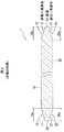
図1(a)は、本発明の実施の形態に係る窒化物半導体基板の表面の概要を示し、(b)は、本発明の実施の形態に係る窒化物半導体基板の裏面の概要を示す。
図1(a)及び(b)を参照する。本実施の形態に係る窒化物半導体基板1は、鏡面加工された表面10と、窒化物半導体基板1の表面10側の縁の少なくとも一部が面取り加工されて形成される第1のエッジ部としての面取り部15と、表面10の反対側の鏡面加工された裏面20と、窒化物半導体基板1の裏面20側の縁の少なくとも一部が面取り加工されて形成される第2のエッジ部としての面取り部25とを備える。面取り部15は所定の面取り幅15aを有して形成される。面取り部25も面取り部15と同様にして、所定の面取り幅25aを有して形成される。
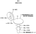
図3は、本発明の実施の形態に係る窒化物半導体基板の製造工程の流れの一例を示す。
本実施の形態に係る窒化物半導体基板1は、表面10の端から窒化物半導体基板1の中心方向に向かって所定の範囲に面取り部15を形成すると共に、面取り部15の表面粗さに対する表面10の表面粗さの比を0.01以下にすると共に、面取り部15の可視光透過率を表面10の可視光透過率の0.2倍以下としたので、可視光又は赤外光が表面10及び面取り部15に照射された場合に、表面10と面取り部15との境界において窒化物半導体基板1の輪郭を光学的に明瞭に把握できる。これにより、本実施の形態に係る窒化物半導体基板1によれば、例えば、光学顕微鏡によって、若しくはステッパー装置、マスクアライナー装置等に搭載された画像処理装置によって、窒化物半導体基板1の輪郭を容易に把握できると共に、窒化物半導体基板1の端部(縁部)を容易に認識できる。
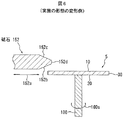
図5は、本発明の実施の形態の変形例に係る窒化物半導体基板の断面の概要を示す。
表面10、面取り部15、裏面20、及び面取り部25のそれぞれを鏡面化すると共に、面取り幅15a及び面取り幅25aを0.5mmにした。そして、面取り部15の平均表面粗さ(Ra)に対する表面10の平均表面粗さ(Ra)の比を0.001にした。なお、表面10のRaは、3nmにした。
面取り部15の平均表面粗さ(Ra)に対する表面10の平均表面粗さ(Ra)の比を0.01にした点を除き、実施例1と同様にして窒化物半導体基板を製造した。
面取り幅15a及び面取り幅25aを0.9mmにすると共に、面取り部15の平均表面粗さ(Ra)に対する表面10の平均表面粗さ(Ra)の比を0.01にした点を除き、実施例1と同様にして窒化物半導体基板を製造した。
一方、比較例1として、面取り部15を形成する面取り加工時に用いる砥石150を#200にすることにより、表面10の平均表面粗さ(Ra)の面取り部15の平均表面粗さ(Ra)に対する比を0.03にした窒化物半導体基板を製造した。
また、比較例2として、表面10及び裏面20に鏡面加工を施す一方で、面取り加工を施さない窒化物半導体基板を製造した(面取り幅15a及び面取り幅25a=0.0mm)。
更に、比較例3として、面取り部15を形成する面取り加工時の用いる砥石150を#3000にすることにより、面取り部15の平均表面粗さ(Ra)に対する表面10の平均表面粗さ(Ra)の比を0.0005にした窒化物半導体基板を製造した。

5 表裏面鏡面加工済み窒化物半導体基板
10 表面
15、25 面取り部
15a、25a 面取り幅
17、27 面取り部表面
20 裏面
30 端部
32 ラウンド部
100 基板吸着ステージ
100a θ方向
100b X方向
100c Y方向
150、152 砥石
150a ω方向
150b Z方向
152a 方向
152b、152c 砥石表面
152d 砥石端部
Claims (6)
- 窒化物半導体からなる基板であって、
前記基板は、表面と、前記表面の反対側の裏面と、前記基板の表面側の縁が面取り加工されて形成される第1のエッジ部とを備え、
前記第1のエッジ部の平均表面粗さに対する前記表面の平均表面粗さの比が0.01以下である窒化物半導体基板。 - 前記基板の裏面側の縁が面取り加工されて形成される第2のエッジ部を
更に備え、
前記第2のエッジ部の平均表面粗さに対する前記裏面の平均表面粗さの比が、0.01以下である請求項1に記載の窒化物半導体基板。 - 前記第1のエッジ部は、前記表面の可視光透過率の0.2倍以下の可視光透過率を有する請求項2に記載の窒化物半導体基板。
- 前記第2のエッジ部は、前記裏面の可視光透過率の0.2倍以下の可視光透過率を有するである請求項3に記載の窒化物半導体基板。
- 窒化物半導体からなる基板の表面を鏡面加工する表面加工工程と、
前記基板の表面側の縁を面取り加工することにより第1のエッジ部を形成する第1エッジ形成工程と
を備え、
前記第1エッジ形成工程は、前記第1のエッジ部の平均表面粗さに対する前記表面の平均表面粗さの比が0.01以下であり、前記第1のエッジ部の可視光透過率が前記表面の可視光透過率の0.2倍以下である前記第1のエッジを形成する窒化物半導体基板の製造方法。 - 前記基板の前記表面とは反対側の裏面を鏡面加工する裏面加工工程と、
前記基板の裏面側の縁を面取り加工することにより第2のエッジ部を形成する第2エッジ形成工程と
を更に備え、
前記第2エッジ形成工程は、前記第2のエッジ部の平均表面粗さに対する前記裏面の平均表面粗さの比が0.01以下であり、前記第2のエッジ部の可視光透過率が前記裏面の可視光透過率の0.2倍以下である前記第2のエッジを形成する請求項5に記載の窒化物半導体基板の製造方法。
Priority Applications (2)
| Application Number | Priority Date | Filing Date | Title |
|---|---|---|---|
| JP2008269880A JP5293074B2 (ja) | 2008-10-20 | 2008-10-20 | 窒化物半導体基板及び窒化物半導体基板の製造方法 |
| US12/585,109 US8120059B2 (en) | 2008-10-20 | 2009-09-03 | Nitride semiconductor substrate and method of fabricating the same |
Applications Claiming Priority (1)
| Application Number | Priority Date | Filing Date | Title |
|---|---|---|---|
| JP2008269880A JP5293074B2 (ja) | 2008-10-20 | 2008-10-20 | 窒化物半導体基板及び窒化物半導体基板の製造方法 |
Publications (2)
| Publication Number | Publication Date |
|---|---|
| JP2010094793A true JP2010094793A (ja) | 2010-04-30 |
| JP5293074B2 JP5293074B2 (ja) | 2013-09-18 |
Family
ID=42107986
Family Applications (1)
| Application Number | Title | Priority Date | Filing Date |
|---|---|---|---|
| JP2008269880A Active JP5293074B2 (ja) | 2008-10-20 | 2008-10-20 | 窒化物半導体基板及び窒化物半導体基板の製造方法 |
Country Status (2)
| Country | Link |
|---|---|
| US (1) | US8120059B2 (ja) |
| JP (1) | JP5293074B2 (ja) |
Cited By (1)
| Publication number | Priority date | Publication date | Assignee | Title |
|---|---|---|---|---|
| JP2023121090A (ja) * | 2022-02-18 | 2023-08-30 | 三安ジャパンテクノロジー株式会社 | 接合ウエハ |
Families Citing this family (2)
| Publication number | Priority date | Publication date | Assignee | Title |
|---|---|---|---|---|
| JP6244962B2 (ja) * | 2014-02-17 | 2017-12-13 | 株式会社Sumco | 半導体ウェーハの製造方法 |
| JP7562994B2 (ja) * | 2020-06-08 | 2024-10-08 | 株式会社Sumco | ウェーハ外周部の研磨装置 |
Citations (7)
| Publication number | Priority date | Publication date | Assignee | Title |
|---|---|---|---|---|
| JP2000074631A (ja) * | 1998-08-31 | 2000-03-14 | Toshiba Ceramics Co Ltd | 面取り幅測定装置 |
| JP2004050347A (ja) * | 2002-07-19 | 2004-02-19 | Mitsutoyo Corp | 研削加工方法、及びこの方法を用いた平面研削盤またはグラインディングセンタ |
| JP2004319951A (ja) * | 2003-04-02 | 2004-11-11 | Sumitomo Electric Ind Ltd | エッジ研磨した窒化物半導体基板とエッジ研磨したGaN自立基板及び窒化物半導体基板のエッジ加工方法 |
| JP2006038983A (ja) * | 2004-07-23 | 2006-02-09 | Seiko Epson Corp | 電気光学装置用基板及びその製造方法、電気光学装置並びに電子機器 |
| JP2006099041A (ja) * | 2004-08-30 | 2006-04-13 | Hoya Corp | マスクブランク用ガラス基板の製造方法、マスクブランクの製造方法、及び露光用マスクの製造方法 |
| JP2007216355A (ja) * | 2006-02-17 | 2007-08-30 | Nidek Co Ltd | カップ取付け装置及び該装置にて使用するためのパターン板 |
| JP2008042213A (ja) * | 2006-08-09 | 2008-02-21 | Siltronic Ag | 極めて正確なエッジプロフィルを備えた半導体ウェハ及びこれを製造する方法 |
Family Cites Families (4)
| Publication number | Priority date | Publication date | Assignee | Title |
|---|---|---|---|---|
| WO2001062436A1 (fr) * | 2000-02-23 | 2001-08-30 | Shin-Etsu Handotai Co., Ltd. | Procede et appareil permettant de polir une partie circulaire exterieure a chanfrein d'une tranche |
| KR100818683B1 (ko) * | 2000-07-10 | 2008-04-01 | 신에츠 한도타이 가부시키가이샤 | 경면 면취 웨이퍼, 경면 면취용 연마 클로스 및 경면 면취연마장치 및 방법 |
| JP4034682B2 (ja) * | 2002-10-21 | 2008-01-16 | 株式会社東芝 | 半導体ウェーハ及び半導体ウェーハ製造方法 |
| JP2010092975A (ja) * | 2008-10-06 | 2010-04-22 | Hitachi Cable Ltd | 窒化物半導体基板 |
-
2008
- 2008-10-20 JP JP2008269880A patent/JP5293074B2/ja active Active
-
2009
- 2009-09-03 US US12/585,109 patent/US8120059B2/en active Active
Patent Citations (7)
| Publication number | Priority date | Publication date | Assignee | Title |
|---|---|---|---|---|
| JP2000074631A (ja) * | 1998-08-31 | 2000-03-14 | Toshiba Ceramics Co Ltd | 面取り幅測定装置 |
| JP2004050347A (ja) * | 2002-07-19 | 2004-02-19 | Mitsutoyo Corp | 研削加工方法、及びこの方法を用いた平面研削盤またはグラインディングセンタ |
| JP2004319951A (ja) * | 2003-04-02 | 2004-11-11 | Sumitomo Electric Ind Ltd | エッジ研磨した窒化物半導体基板とエッジ研磨したGaN自立基板及び窒化物半導体基板のエッジ加工方法 |
| JP2006038983A (ja) * | 2004-07-23 | 2006-02-09 | Seiko Epson Corp | 電気光学装置用基板及びその製造方法、電気光学装置並びに電子機器 |
| JP2006099041A (ja) * | 2004-08-30 | 2006-04-13 | Hoya Corp | マスクブランク用ガラス基板の製造方法、マスクブランクの製造方法、及び露光用マスクの製造方法 |
| JP2007216355A (ja) * | 2006-02-17 | 2007-08-30 | Nidek Co Ltd | カップ取付け装置及び該装置にて使用するためのパターン板 |
| JP2008042213A (ja) * | 2006-08-09 | 2008-02-21 | Siltronic Ag | 極めて正確なエッジプロフィルを備えた半導体ウェハ及びこれを製造する方法 |
Cited By (1)
| Publication number | Priority date | Publication date | Assignee | Title |
|---|---|---|---|---|
| JP2023121090A (ja) * | 2022-02-18 | 2023-08-30 | 三安ジャパンテクノロジー株式会社 | 接合ウエハ |
Also Published As
| Publication number | Publication date |
|---|---|
| US8120059B2 (en) | 2012-02-21 |
| US20100096728A1 (en) | 2010-04-22 |
| JP5293074B2 (ja) | 2013-09-18 |
Similar Documents
| Publication | Publication Date | Title |
|---|---|---|
| US11911842B2 (en) | Laser-assisted method for parting crystalline material | |
| US7118813B2 (en) | Vicinal gallium nitride substrate for high quality homoepitaxy | |
| US8062960B2 (en) | Compound semiconductor device and method of manufacturing compound semiconductor device | |
| CN100424817C (zh) | 半导体用氮化物衬底的制备方法及氮化物半导体衬底 | |
| EP2543752A1 (en) | Internal reforming substrate for epitaxial growth, internal reforming substrate with multilayer film, semiconductor device, bulk semiconductor substrate, and production methods therefor | |
| CN1090382C (zh) | Iii-v族化合物半导体晶片 | |
| US7986030B2 (en) | Nitride semiconductor substrate | |
| CN109312491B (zh) | 氮化物半导体模板、氮化物半导体模板的制造方法以及氮化物半导体自支撑基板的制造方法 | |
| US9938638B2 (en) | Method for producing semiconductor epitaxial wafer and semiconductor epitaxial wafer | |
| EP2378542A1 (en) | Substrate and method for manufacturing substrate | |
| JP5293074B2 (ja) | 窒化物半導体基板及び窒化物半導体基板の製造方法 | |
| US7374618B2 (en) | Group III nitride semiconductor substrate | |
| JP2008115074A (ja) | 窒化ガリウム単結晶基板及び表面加工方法 | |
| WO2022004046A1 (ja) | エピタキシャル結晶成長用自立基板および機能素子 | |
| JP5332691B2 (ja) | 窒化物半導体基板の加工方法 | |
| JP6978641B1 (ja) | Iii族元素窒化物半導体基板 | |
| JP2005032804A (ja) | 半導体ウェハの加工方法 | |
| JP5126108B2 (ja) | 窒化物半導体基板 | |
| WO2022059244A1 (ja) | Iii族元素窒化物半導体基板 | |
| CN105097893A (zh) | Iii族氮化物衬底以及制备工艺 | |
| JP2004165484A (ja) | 半導体ウェハの加工方法 | |
| HK1122140A (en) | Method of manufacturing nitride substrate for semiconductors, and nitride semiconductor substrate |
Legal Events
| Date | Code | Title | Description |
|---|---|---|---|
| A621 | Written request for application examination |
Free format text: JAPANESE INTERMEDIATE CODE: A621 Effective date: 20101217 |
|
| A131 | Notification of reasons for refusal |
Free format text: JAPANESE INTERMEDIATE CODE: A131 Effective date: 20120911 |
|
| A977 | Report on retrieval |
Free format text: JAPANESE INTERMEDIATE CODE: A971007 Effective date: 20120913 |
|
| A521 | Request for written amendment filed |
Free format text: JAPANESE INTERMEDIATE CODE: A523 Effective date: 20121106 |
|
| TRDD | Decision of grant or rejection written | ||
| A01 | Written decision to grant a patent or to grant a registration (utility model) |
Free format text: JAPANESE INTERMEDIATE CODE: A01 Effective date: 20130514 |
|
| A61 | First payment of annual fees (during grant procedure) |
Free format text: JAPANESE INTERMEDIATE CODE: A61 Effective date: 20130527 |
|
| R150 | Certificate of patent or registration of utility model |
Ref document number: 5293074 Country of ref document: JP Free format text: JAPANESE INTERMEDIATE CODE: R150 Free format text: JAPANESE INTERMEDIATE CODE: R150 |
|
| S111 | Request for change of ownership or part of ownership |
Free format text: JAPANESE INTERMEDIATE CODE: R313111 |
|
| R350 | Written notification of registration of transfer |
Free format text: JAPANESE INTERMEDIATE CODE: R350 |
|
| S111 | Request for change of ownership or part of ownership |
Free format text: JAPANESE INTERMEDIATE CODE: R313111 |
|
| R350 | Written notification of registration of transfer |
Free format text: JAPANESE INTERMEDIATE CODE: R350 |
|
| S111 | Request for change of ownership or part of ownership |
Free format text: JAPANESE INTERMEDIATE CODE: R313113 |
|
| R350 | Written notification of registration of transfer |
Free format text: JAPANESE INTERMEDIATE CODE: R350 |
|
| S531 | Written request for registration of change of domicile |
Free format text: JAPANESE INTERMEDIATE CODE: R313531 |
|
| R350 | Written notification of registration of transfer |
Free format text: JAPANESE INTERMEDIATE CODE: R350 |