JP2010074158A - ローカルインタコネクトを備えた半導体装置 - Google Patents
ローカルインタコネクトを備えた半導体装置 Download PDFInfo
- Publication number
- JP2010074158A JP2010074158A JP2009207011A JP2009207011A JP2010074158A JP 2010074158 A JP2010074158 A JP 2010074158A JP 2009207011 A JP2009207011 A JP 2009207011A JP 2009207011 A JP2009207011 A JP 2009207011A JP 2010074158 A JP2010074158 A JP 2010074158A
- Authority
- JP
- Japan
- Prior art keywords
- pair
- gate line
- line structure
- semiconductor device
- gate
- Prior art date
- Legal status (The legal status is an assumption and is not a legal conclusion. Google has not performed a legal analysis and makes no representation as to the accuracy of the status listed.)
- Granted
Links
Images


Classifications
-
- H10W20/0698—
-
- H—ELECTRICITY
- H10—SEMICONDUCTOR DEVICES; ELECTRIC SOLID-STATE DEVICES NOT OTHERWISE PROVIDED FOR
- H10D—INORGANIC ELECTRIC SEMICONDUCTOR DEVICES
- H10D64/00—Electrodes of devices having potential barriers
- H10D64/20—Electrodes characterised by their shapes, relative sizes or dispositions
- H10D64/23—Electrodes carrying the current to be rectified, amplified, oscillated or switched, e.g. sources, drains, anodes or cathodes
- H10D64/251—Source or drain electrodes for field-effect devices
-
- H—ELECTRICITY
- H10—SEMICONDUCTOR DEVICES; ELECTRIC SOLID-STATE DEVICES NOT OTHERWISE PROVIDED FOR
- H10D—INORGANIC ELECTRIC SEMICONDUCTOR DEVICES
- H10D64/00—Electrodes of devices having potential barriers
- H10D64/20—Electrodes characterised by their shapes, relative sizes or dispositions
- H10D64/27—Electrodes not carrying the current to be rectified, amplified, oscillated or switched, e.g. gates
- H10D64/311—Gate electrodes for field-effect devices
- H10D64/411—Gate electrodes for field-effect devices for FETs
- H10D64/511—Gate electrodes for field-effect devices for FETs for IGFETs
- H10D64/517—Gate electrodes for field-effect devices for FETs for IGFETs characterised by the conducting layers
- H10D64/519—Gate electrodes for field-effect devices for FETs for IGFETs characterised by the conducting layers characterised by their top-view geometrical layouts
-
- H—ELECTRICITY
- H10—SEMICONDUCTOR DEVICES; ELECTRIC SOLID-STATE DEVICES NOT OTHERWISE PROVIDED FOR
- H10D—INORGANIC ELECTRIC SEMICONDUCTOR DEVICES
- H10D84/00—Integrated devices formed in or on semiconductor substrates that comprise only semiconducting layers, e.g. on Si wafers or on GaAs-on-Si wafers
- H10D84/01—Manufacture or treatment
- H10D84/0123—Integrating together multiple components covered by H10D12/00 or H10D30/00, e.g. integrating multiple IGBTs
- H10D84/0126—Integrating together multiple components covered by H10D12/00 or H10D30/00, e.g. integrating multiple IGBTs the components including insulated gates, e.g. IGFETs
- H10D84/0149—Manufacturing their interconnections or electrodes, e.g. source or drain electrodes
-
- H—ELECTRICITY
- H10—SEMICONDUCTOR DEVICES; ELECTRIC SOLID-STATE DEVICES NOT OTHERWISE PROVIDED FOR
- H10D—INORGANIC ELECTRIC SEMICONDUCTOR DEVICES
- H10D84/00—Integrated devices formed in or on semiconductor substrates that comprise only semiconducting layers, e.g. on Si wafers or on GaAs-on-Si wafers
- H10D84/01—Manufacture or treatment
- H10D84/02—Manufacture or treatment characterised by using material-based technologies
- H10D84/03—Manufacture or treatment characterised by using material-based technologies using Group IV technology, e.g. silicon technology or silicon-carbide [SiC] technology
- H10D84/038—Manufacture or treatment characterised by using material-based technologies using Group IV technology, e.g. silicon technology or silicon-carbide [SiC] technology using silicon technology, e.g. SiGe
-
- H—ELECTRICITY
- H10—SEMICONDUCTOR DEVICES; ELECTRIC SOLID-STATE DEVICES NOT OTHERWISE PROVIDED FOR
- H10D—INORGANIC ELECTRIC SEMICONDUCTOR DEVICES
- H10D84/00—Integrated devices formed in or on semiconductor substrates that comprise only semiconducting layers, e.g. on Si wafers or on GaAs-on-Si wafers
- H10D84/80—Integrated devices formed in or on semiconductor substrates that comprise only semiconducting layers, e.g. on Si wafers or on GaAs-on-Si wafers characterised by the integration of at least one component covered by groups H10D12/00 or H10D30/00, e.g. integration of IGFETs
- H10D84/82—Integrated devices formed in or on semiconductor substrates that comprise only semiconducting layers, e.g. on Si wafers or on GaAs-on-Si wafers characterised by the integration of at least one component covered by groups H10D12/00 or H10D30/00, e.g. integration of IGFETs of only field-effect components
- H10D84/83—Integrated devices formed in or on semiconductor substrates that comprise only semiconducting layers, e.g. on Si wafers or on GaAs-on-Si wafers characterised by the integration of at least one component covered by groups H10D12/00 or H10D30/00, e.g. integration of IGFETs of only field-effect components of only insulated-gate FETs [IGFET]
Landscapes
- Internal Circuitry In Semiconductor Integrated Circuit Devices (AREA)
- Semiconductor Integrated Circuits (AREA)
- Electrodes Of Semiconductors (AREA)
- Metal-Oxide And Bipolar Metal-Oxide Semiconductor Integrated Circuits (AREA)
- Insulated Gate Type Field-Effect Transistor (AREA)
Abstract
【解決手段】ローカルインタコネクトを備えた半導体装置であって、基板上に配置され、実質的に同一線上にある第1ゲート線構造と第2ゲート線構造、前記第1ゲート線構造の両側の前記基板に形成された第1対ソース/ドレイン領域と前記第2ゲート線構造の両側の前記基板に形成された第2対ソース/ドレイン領域、及び前記第1ゲート線構造と前記第2ゲート線構造の両側の前記基板上に配置され、それらが前記第1対ソース/ドレイン領域のうちの1つと前記第2対ソース/ドレイン領域のうちの1つに接続された一対の導電線を含む半導体装置。
【選択図】図1
Description
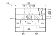
100a、100b 活性層
101 第1対ソース/ドレイン領域
103 第2対ソース/ドレイン領域
110 分離構造
111 ゲート誘電体層
112 導電線
113 ゲート電極
115 ゲートスペーサ
116 第1ゲート線構造
118 第2ゲート線構造
120、130 誘電体層
132 導電プラグ
136 金属層
200 半導体装置
Claims (10)
- ローカルインタコネクトを備えた半導体装置であって、
基板上に配置され、実質的に同一線上にある第1ゲート線構造と第2ゲート線構造、
前記第1ゲート線構造の両側の前記基板に形成された第1対ソース/ドレイン領域と前記第2ゲート線構造の両側の前記基板に形成された第2対ソース/ドレイン領域、及び
前記第1ゲート線構造と前記第2ゲート線構造の両側の前記基板上に配置され、それらが前記第1対ソース/ドレイン領域のうちの1つと前記第2対ソース/ドレイン領域のうちの1つに接続された一対の導電線を含む半導体装置。 - 前記第1ゲート線構造と前記第2ゲート線構造のそれぞれは、
前記基板上に配置されたゲート誘電体層、
前記ゲート誘電体層上に配置されたゲート電極、及び
前記ゲート電極の側壁に配置されたゲートスペーサを含む請求項1に記載の半導体装置。 - 前記ゲート電極は、ポリシリコンを含む請求項2に記載の半導体装置。
- 前記一対の導電線は、前記ゲート電極と同じレベルにある請求項2に記載の半導体装置。
- 前記第1と第2対ソース/ドレイン領域は、同じ導電型を有する請求項2に記載の半導体装置。
- 前記第1ゲート線構造と前記第2ゲート線構造の前記ゲート電極は、一体成形される請求項5に記載の半導体装置。
- 前記第1と第2対ソース/ドレイン領域は、異なる導電型を有する請求項1に記載の半導体装置。
- 前記一対の導電線は、実質的に前記第1ゲート線構造と前記第2ゲート線構造に平行する請求項1に記載の半導体装置。
- 前記一対のインタコネクト層は、タングステンを含む請求項1に記載の半導体装置。
- 前記一対の導電線に配置され、前記一対の導電線のうちの1つに接続された少なくとも1つの導電プラグ、及び
前記導電プラグに配置され、そこに接続される金属層を更に含む請求項1に記載の半導体装置。
Applications Claiming Priority (2)
| Application Number | Priority Date | Filing Date | Title |
|---|---|---|---|
| US12/212,034 | 2008-09-17 | ||
| US12/212,034 US8138554B2 (en) | 2008-09-17 | 2008-09-17 | Semiconductor device with local interconnects |
Publications (2)
| Publication Number | Publication Date |
|---|---|
| JP2010074158A true JP2010074158A (ja) | 2010-04-02 |
| JP5388768B2 JP5388768B2 (ja) | 2014-01-15 |
Family
ID=42006445
Family Applications (1)
| Application Number | Title | Priority Date | Filing Date |
|---|---|---|---|
| JP2009207011A Active JP5388768B2 (ja) | 2008-09-17 | 2009-09-08 | ローカルインターコネクトを備えた半導体装置 |
Country Status (5)
| Country | Link |
|---|---|
| US (1) | US8138554B2 (ja) |
| JP (1) | JP5388768B2 (ja) |
| KR (1) | KR101203936B1 (ja) |
| CN (1) | CN101677102B (ja) |
| TW (1) | TWI396254B (ja) |
Cited By (4)
| Publication number | Priority date | Publication date | Assignee | Title |
|---|---|---|---|---|
| JP2014220501A (ja) * | 2013-05-02 | 2014-11-20 | 台湾積體電路製造股▲ふん▼有限公司Taiwan Semiconductor Manufacturing Company,Ltd. | ポリシリコン構造の真上の標準セル金属構造物 |
| JP2016507909A (ja) * | 2013-03-14 | 2016-03-10 | クアルコム,インコーポレイテッド | 高密度用ローカルインターコネクト構造 |
| JP2017510069A (ja) * | 2014-03-03 | 2017-04-06 | クアルコム,インコーポレイテッド | 高性能標準セル |
| US10692808B2 (en) | 2017-09-18 | 2020-06-23 | Qualcomm Incorporated | High performance cell design in a technology with high density metal routing |
Families Citing this family (7)
| Publication number | Priority date | Publication date | Assignee | Title |
|---|---|---|---|---|
| DE102013110607B4 (de) * | 2013-05-02 | 2020-02-27 | Taiwan Semiconductor Manufacturing Company, Ltd. | Standardzellen-Metallstruktur direkt über Polysiliziumstruktur |
| US10177133B2 (en) | 2014-05-16 | 2019-01-08 | Taiwan Semiconductor Manufacturing Co., Ltd. | Semiconductor device including source/drain contact having height below gate stack |
| US9349859B1 (en) | 2015-01-29 | 2016-05-24 | Taiwan Semiconductor Manufacturing Company, Ltd. | Top metal pads as local interconnectors of vertical transistors |
| US10510688B2 (en) * | 2015-10-26 | 2019-12-17 | Taiwan Semiconductor Manufacturing Co., Ltd. | Via rail solution for high power electromigration |
| CN106653679A (zh) * | 2015-11-03 | 2017-05-10 | 中芯国际集成电路制造(上海)有限公司 | 半导体器件及其形成方法 |
| US10672708B2 (en) | 2015-11-30 | 2020-06-02 | Taiwan Semiconductor Manufacturing Co., Ltd. | Standard-cell layout structure with horn power and smart metal cut |
| DE102016114779B4 (de) * | 2016-05-19 | 2025-08-07 | Taiwan Semiconductor Manufacturing Company, Ltd. | Halbleiterstruktur und verfahren zu ihrer herstellung |
Citations (7)
| Publication number | Priority date | Publication date | Assignee | Title |
|---|---|---|---|---|
| JPH0395957A (ja) * | 1989-09-08 | 1991-04-22 | Toshiba Corp | 半導体論理集積回路 |
| JPH06204438A (ja) * | 1992-12-28 | 1994-07-22 | Kawasaki Steel Corp | 半導体装置 |
| JPH07245396A (ja) * | 1994-03-04 | 1995-09-19 | Sharp Corp | 半導体装置及びその製造方法 |
| JP2000114262A (ja) * | 1998-10-05 | 2000-04-21 | Toshiba Corp | 半導体装置及びその製造方法 |
| JP2006157044A (ja) * | 2001-01-30 | 2006-06-15 | Renesas Technology Corp | 半導体集積回路装置の製造方法 |
| JP2006202908A (ja) * | 2005-01-19 | 2006-08-03 | Matsushita Electric Ind Co Ltd | 半導体装置の配線構造、その製造方法および回路基板 |
| US20070181942A1 (en) * | 2006-01-16 | 2007-08-09 | Gerhard Knoblinger | Semiconductor circuit arrangement |
Family Cites Families (5)
| Publication number | Priority date | Publication date | Assignee | Title |
|---|---|---|---|---|
| JP2004111746A (ja) | 2002-09-19 | 2004-04-08 | Fujitsu Ltd | 半導体装置及びその製造方法 |
| US20050064629A1 (en) * | 2003-09-22 | 2005-03-24 | Chen-Hua Yu | Tungsten-copper interconnect and method for fabricating the same |
| US7701034B2 (en) * | 2005-01-21 | 2010-04-20 | Taiwan Semiconductor Manufacturing Company, Ltd. | Dummy patterns in integrated circuit fabrication |
| US7345344B2 (en) * | 2006-02-16 | 2008-03-18 | Freescale Semiconductor, Inc. | Embedded substrate interconnect for underside contact to source and drain regions |
| US7733698B2 (en) * | 2007-03-21 | 2010-06-08 | Qimonda Ag | Memory device, a non-volatile semiconductor memory device and a method of forming a memory device |
-
2008
- 2008-09-17 US US12/212,034 patent/US8138554B2/en active Active
-
2009
- 2009-09-08 JP JP2009207011A patent/JP5388768B2/ja active Active
- 2009-09-16 CN CN2009101734177A patent/CN101677102B/zh active Active
- 2009-09-16 KR KR1020090087579A patent/KR101203936B1/ko active Active
- 2009-09-17 TW TW098131332A patent/TWI396254B/zh active
Patent Citations (7)
| Publication number | Priority date | Publication date | Assignee | Title |
|---|---|---|---|---|
| JPH0395957A (ja) * | 1989-09-08 | 1991-04-22 | Toshiba Corp | 半導体論理集積回路 |
| JPH06204438A (ja) * | 1992-12-28 | 1994-07-22 | Kawasaki Steel Corp | 半導体装置 |
| JPH07245396A (ja) * | 1994-03-04 | 1995-09-19 | Sharp Corp | 半導体装置及びその製造方法 |
| JP2000114262A (ja) * | 1998-10-05 | 2000-04-21 | Toshiba Corp | 半導体装置及びその製造方法 |
| JP2006157044A (ja) * | 2001-01-30 | 2006-06-15 | Renesas Technology Corp | 半導体集積回路装置の製造方法 |
| JP2006202908A (ja) * | 2005-01-19 | 2006-08-03 | Matsushita Electric Ind Co Ltd | 半導体装置の配線構造、その製造方法および回路基板 |
| US20070181942A1 (en) * | 2006-01-16 | 2007-08-09 | Gerhard Knoblinger | Semiconductor circuit arrangement |
Cited By (5)
| Publication number | Priority date | Publication date | Assignee | Title |
|---|---|---|---|---|
| JP2016507909A (ja) * | 2013-03-14 | 2016-03-10 | クアルコム,インコーポレイテッド | 高密度用ローカルインターコネクト構造 |
| JP2014220501A (ja) * | 2013-05-02 | 2014-11-20 | 台湾積體電路製造股▲ふん▼有限公司Taiwan Semiconductor Manufacturing Company,Ltd. | ポリシリコン構造の真上の標準セル金属構造物 |
| US9158877B2 (en) | 2013-05-02 | 2015-10-13 | Taiwan Semiconductor Manufacturing Company, Ltd. | Standard cell metal structure directly over polysilicon structure |
| JP2017510069A (ja) * | 2014-03-03 | 2017-04-06 | クアルコム,インコーポレイテッド | 高性能標準セル |
| US10692808B2 (en) | 2017-09-18 | 2020-06-23 | Qualcomm Incorporated | High performance cell design in a technology with high density metal routing |
Also Published As
| Publication number | Publication date |
|---|---|
| KR101203936B1 (ko) | 2012-11-23 |
| CN101677102B (zh) | 2012-02-08 |
| TW201013842A (en) | 2010-04-01 |
| US8138554B2 (en) | 2012-03-20 |
| KR20100032344A (ko) | 2010-03-25 |
| US20100065921A1 (en) | 2010-03-18 |
| JP5388768B2 (ja) | 2014-01-15 |
| TWI396254B (zh) | 2013-05-11 |
| CN101677102A (zh) | 2010-03-24 |
Similar Documents
| Publication | Publication Date | Title |
|---|---|---|
| JP5388768B2 (ja) | ローカルインターコネクトを備えた半導体装置 | |
| TW202115849A (zh) | 半導體元件及其製造方法 | |
| KR100491458B1 (ko) | 반도체 장치 | |
| CN100559579C (zh) | 具有自对准接触的半导体器件及其制造方法 | |
| CN106033741B (zh) | 金属内连线结构及其制作方法 | |
| KR100499175B1 (ko) | 반도체 장치 및 이의 제조 방법 | |
| US8624328B2 (en) | Semiconductor device | |
| US20100032810A1 (en) | Through wafer vias and method of making same | |
| US11437313B2 (en) | Structure and method of forming a semiconductor device with resistive elements | |
| JP3590034B2 (ja) | 半導体容量素子及びその製造方法 | |
| KR100791339B1 (ko) | 평탄화 저항 패턴을 포함하는 복합칩 반도체 소자 및 그제조 방법 | |
| US6642604B2 (en) | Semiconductor device with resistor layer having heat radiation path to semiconductor substrate | |
| WO2000067324A1 (fr) | Circuit integre, son procede de fabrication, et procede de production d'un dessin de masque | |
| CN107706233B (zh) | 半导体元件及其制作方法 | |
| US7768128B2 (en) | Semiconductor memory devices including a damascene wiring line | |
| CN102122651B (zh) | 半导体器件及其制造方法 | |
| KR100650192B1 (ko) | 반도체 소자 및 그의 형성 방법 | |
| CN114944360A (zh) | 半导体装置及其制造方法 | |
| US6776622B2 (en) | Conductive contact structure and process for producing the same | |
| KR20220071569A (ko) | 3차원 적층 반도체 소자 및 그 제조 방법 | |
| JP2004104136A (ja) | 半導体集積回路装置の製造方法およびマスクパターンの生成方法 | |
| TWI555122B (zh) | 半導體元件之內連線結構其製備方法 | |
| JP4201156B2 (ja) | 半導体装置及びその製造方法 | |
| KR20240163457A (ko) | 반도체 장치 및 그 제조 방법 | |
| KR0172725B1 (ko) | 반도체 소자의 다층 금속배선 형성방법 |
Legal Events
| Date | Code | Title | Description |
|---|---|---|---|
| A131 | Notification of reasons for refusal |
Free format text: JAPANESE INTERMEDIATE CODE: A131 Effective date: 20120522 |
|
| A977 | Report on retrieval |
Free format text: JAPANESE INTERMEDIATE CODE: A971007 Effective date: 20120524 |
|
| A601 | Written request for extension of time |
Free format text: JAPANESE INTERMEDIATE CODE: A601 Effective date: 20120820 |
|
| A602 | Written permission of extension of time |
Free format text: JAPANESE INTERMEDIATE CODE: A602 Effective date: 20120823 |
|
| A521 | Request for written amendment filed |
Free format text: JAPANESE INTERMEDIATE CODE: A523 Effective date: 20120924 |
|
| A131 | Notification of reasons for refusal |
Free format text: JAPANESE INTERMEDIATE CODE: A131 Effective date: 20130319 |
|
| A521 | Request for written amendment filed |
Free format text: JAPANESE INTERMEDIATE CODE: A523 Effective date: 20130617 |
|
| TRDD | Decision of grant or rejection written | ||
| A01 | Written decision to grant a patent or to grant a registration (utility model) |
Free format text: JAPANESE INTERMEDIATE CODE: A01 Effective date: 20130910 |
|
| A61 | First payment of annual fees (during grant procedure) |
Free format text: JAPANESE INTERMEDIATE CODE: A61 Effective date: 20131008 |
|
| R150 | Certificate of patent or registration of utility model |
Ref document number: 5388768 Country of ref document: JP Free format text: JAPANESE INTERMEDIATE CODE: R150 Free format text: JAPANESE INTERMEDIATE CODE: R150 |
|
| R250 | Receipt of annual fees |
Free format text: JAPANESE INTERMEDIATE CODE: R250 |
|
| R250 | Receipt of annual fees |
Free format text: JAPANESE INTERMEDIATE CODE: R250 |
|
| R250 | Receipt of annual fees |
Free format text: JAPANESE INTERMEDIATE CODE: R250 |
|
| R250 | Receipt of annual fees |
Free format text: JAPANESE INTERMEDIATE CODE: R250 |
|
| R250 | Receipt of annual fees |
Free format text: JAPANESE INTERMEDIATE CODE: R250 |
|
| R250 | Receipt of annual fees |
Free format text: JAPANESE INTERMEDIATE CODE: R250 |
|
| R250 | Receipt of annual fees |
Free format text: JAPANESE INTERMEDIATE CODE: R250 |
|
| R250 | Receipt of annual fees |
Free format text: JAPANESE INTERMEDIATE CODE: R250 |
|
| R250 | Receipt of annual fees |
Free format text: JAPANESE INTERMEDIATE CODE: R250 |
|
| R250 | Receipt of annual fees |
Free format text: JAPANESE INTERMEDIATE CODE: R250 |