JP2010074158A - Semiconductor device with local interconnect - Google Patents
Semiconductor device with local interconnect Download PDFInfo
- Publication number
- JP2010074158A JP2010074158A JP2009207011A JP2009207011A JP2010074158A JP 2010074158 A JP2010074158 A JP 2010074158A JP 2009207011 A JP2009207011 A JP 2009207011A JP 2009207011 A JP2009207011 A JP 2009207011A JP 2010074158 A JP2010074158 A JP 2010074158A
- Authority
- JP
- Japan
- Prior art keywords
- pair
- line structure
- gate line
- semiconductor device
- gate
- Prior art date
- Legal status (The legal status is an assumption and is not a legal conclusion. Google has not performed a legal analysis and makes no representation as to the accuracy of the status listed.)
- Granted
Links
- 239000004065 semiconductor Substances 0.000 title claims abstract description 32
- 239000000758 substrate Substances 0.000 claims abstract description 27
- 229910052751 metal Inorganic materials 0.000 claims description 7
- 239000002184 metal Substances 0.000 claims description 7
- 125000006850 spacer group Chemical group 0.000 claims description 3
- WFKWXMTUELFFGS-UHFFFAOYSA-N tungsten Chemical compound [W] WFKWXMTUELFFGS-UHFFFAOYSA-N 0.000 claims description 3
- 229910052721 tungsten Inorganic materials 0.000 claims description 3
- 239000010937 tungsten Substances 0.000 claims description 3
- 229910021420 polycrystalline silicon Inorganic materials 0.000 claims description 2
- 229920005591 polysilicon Polymers 0.000 claims description 2
- 239000010410 layer Substances 0.000 description 34
- 238000000034 method Methods 0.000 description 6
- RYGMFSIKBFXOCR-UHFFFAOYSA-N Copper Chemical compound [Cu] RYGMFSIKBFXOCR-UHFFFAOYSA-N 0.000 description 3
- 229910052802 copper Inorganic materials 0.000 description 3
- 239000010949 copper Substances 0.000 description 3
- 230000009977 dual effect Effects 0.000 description 3
- 238000002955 isolation Methods 0.000 description 3
- VYPSYNLAJGMNEJ-UHFFFAOYSA-N Silicium dioxide Chemical compound O=[Si]=O VYPSYNLAJGMNEJ-UHFFFAOYSA-N 0.000 description 2
- 239000005380 borophosphosilicate glass Substances 0.000 description 2
- 238000005530 etching Methods 0.000 description 2
- 239000011229 interlayer Substances 0.000 description 2
- 239000000463 material Substances 0.000 description 2
- 239000005360 phosphosilicate glass Substances 0.000 description 2
- 238000000206 photolithography Methods 0.000 description 2
- 229910052581 Si3N4 Inorganic materials 0.000 description 1
- XUIMIQQOPSSXEZ-UHFFFAOYSA-N Silicon Chemical compound [Si] XUIMIQQOPSSXEZ-UHFFFAOYSA-N 0.000 description 1
- 229910052782 aluminium Inorganic materials 0.000 description 1
- XAGFODPZIPBFFR-UHFFFAOYSA-N aluminium Chemical compound [Al] XAGFODPZIPBFFR-UHFFFAOYSA-N 0.000 description 1
- 230000015572 biosynthetic process Effects 0.000 description 1
- 239000003990 capacitor Substances 0.000 description 1
- 230000007423 decrease Effects 0.000 description 1
- 238000011982 device technology Methods 0.000 description 1
- 238000001459 lithography Methods 0.000 description 1
- 238000004519 manufacturing process Methods 0.000 description 1
- 238000012986 modification Methods 0.000 description 1
- 230000004048 modification Effects 0.000 description 1
- 238000000059 patterning Methods 0.000 description 1
- 229910052710 silicon Inorganic materials 0.000 description 1
- 239000010703 silicon Substances 0.000 description 1
- 235000012239 silicon dioxide Nutrition 0.000 description 1
- 239000000377 silicon dioxide Substances 0.000 description 1
- HQVNEWCFYHHQES-UHFFFAOYSA-N silicon nitride Chemical compound N12[Si]34N5[Si]62N3[Si]51N64 HQVNEWCFYHHQES-UHFFFAOYSA-N 0.000 description 1
- 239000002356 single layer Substances 0.000 description 1
Images


Classifications
-
- H—ELECTRICITY
- H01—ELECTRIC ELEMENTS
- H01L—SEMICONDUCTOR DEVICES NOT COVERED BY CLASS H10
- H01L21/00—Processes or apparatus adapted for the manufacture or treatment of semiconductor or solid state devices or of parts thereof
- H01L21/70—Manufacture or treatment of devices consisting of a plurality of solid state components formed in or on a common substrate or of parts thereof; Manufacture of integrated circuit devices or of parts thereof
- H01L21/71—Manufacture of specific parts of devices defined in group H01L21/70
- H01L21/768—Applying interconnections to be used for carrying current between separate components within a device comprising conductors and dielectrics
- H01L21/76838—Applying interconnections to be used for carrying current between separate components within a device comprising conductors and dielectrics characterised by the formation and the after-treatment of the conductors
- H01L21/76895—Local interconnects; Local pads, as exemplified by patent document EP0896365
-
- H—ELECTRICITY
- H01—ELECTRIC ELEMENTS
- H01L—SEMICONDUCTOR DEVICES NOT COVERED BY CLASS H10
- H01L21/00—Processes or apparatus adapted for the manufacture or treatment of semiconductor or solid state devices or of parts thereof
- H01L21/70—Manufacture or treatment of devices consisting of a plurality of solid state components formed in or on a common substrate or of parts thereof; Manufacture of integrated circuit devices or of parts thereof
- H01L21/77—Manufacture or treatment of devices consisting of a plurality of solid state components or integrated circuits formed in, or on, a common substrate
- H01L21/78—Manufacture or treatment of devices consisting of a plurality of solid state components or integrated circuits formed in, or on, a common substrate with subsequent division of the substrate into plural individual devices
- H01L21/82—Manufacture or treatment of devices consisting of a plurality of solid state components or integrated circuits formed in, or on, a common substrate with subsequent division of the substrate into plural individual devices to produce devices, e.g. integrated circuits, each consisting of a plurality of components
- H01L21/822—Manufacture or treatment of devices consisting of a plurality of solid state components or integrated circuits formed in, or on, a common substrate with subsequent division of the substrate into plural individual devices to produce devices, e.g. integrated circuits, each consisting of a plurality of components the substrate being a semiconductor, using silicon technology
- H01L21/8232—Field-effect technology
- H01L21/8234—MIS technology, i.e. integration processes of field effect transistors of the conductor-insulator-semiconductor type
- H01L21/823475—MIS technology, i.e. integration processes of field effect transistors of the conductor-insulator-semiconductor type interconnection or wiring or contact manufacturing related aspects
-
- H—ELECTRICITY
- H01—ELECTRIC ELEMENTS
- H01L—SEMICONDUCTOR DEVICES NOT COVERED BY CLASS H10
- H01L27/00—Devices consisting of a plurality of semiconductor or other solid-state components formed in or on a common substrate
- H01L27/02—Devices consisting of a plurality of semiconductor or other solid-state components formed in or on a common substrate including semiconductor components specially adapted for rectifying, oscillating, amplifying or switching and having at least one potential-jump barrier or surface barrier; including integrated passive circuit elements with at least one potential-jump barrier or surface barrier
- H01L27/04—Devices consisting of a plurality of semiconductor or other solid-state components formed in or on a common substrate including semiconductor components specially adapted for rectifying, oscillating, amplifying or switching and having at least one potential-jump barrier or surface barrier; including integrated passive circuit elements with at least one potential-jump barrier or surface barrier the substrate being a semiconductor body
- H01L27/08—Devices consisting of a plurality of semiconductor or other solid-state components formed in or on a common substrate including semiconductor components specially adapted for rectifying, oscillating, amplifying or switching and having at least one potential-jump barrier or surface barrier; including integrated passive circuit elements with at least one potential-jump barrier or surface barrier the substrate being a semiconductor body including only semiconductor components of a single kind
- H01L27/085—Devices consisting of a plurality of semiconductor or other solid-state components formed in or on a common substrate including semiconductor components specially adapted for rectifying, oscillating, amplifying or switching and having at least one potential-jump barrier or surface barrier; including integrated passive circuit elements with at least one potential-jump barrier or surface barrier the substrate being a semiconductor body including only semiconductor components of a single kind including field-effect components only
- H01L27/088—Devices consisting of a plurality of semiconductor or other solid-state components formed in or on a common substrate including semiconductor components specially adapted for rectifying, oscillating, amplifying or switching and having at least one potential-jump barrier or surface barrier; including integrated passive circuit elements with at least one potential-jump barrier or surface barrier the substrate being a semiconductor body including only semiconductor components of a single kind including field-effect components only the components being field-effect transistors with insulated gate
-
- H—ELECTRICITY
- H01—ELECTRIC ELEMENTS
- H01L—SEMICONDUCTOR DEVICES NOT COVERED BY CLASS H10
- H01L29/00—Semiconductor devices adapted for rectifying, amplifying, oscillating or switching, or capacitors or resistors with at least one potential-jump barrier or surface barrier, e.g. PN junction depletion layer or carrier concentration layer; Details of semiconductor bodies or of electrodes thereof ; Multistep manufacturing processes therefor
- H01L29/40—Electrodes ; Multistep manufacturing processes therefor
- H01L29/41—Electrodes ; Multistep manufacturing processes therefor characterised by their shape, relative sizes or dispositions
- H01L29/417—Electrodes ; Multistep manufacturing processes therefor characterised by their shape, relative sizes or dispositions carrying the current to be rectified, amplified or switched
- H01L29/41725—Source or drain electrodes for field effect devices
-
- H—ELECTRICITY
- H01—ELECTRIC ELEMENTS
- H01L—SEMICONDUCTOR DEVICES NOT COVERED BY CLASS H10
- H01L29/00—Semiconductor devices adapted for rectifying, amplifying, oscillating or switching, or capacitors or resistors with at least one potential-jump barrier or surface barrier, e.g. PN junction depletion layer or carrier concentration layer; Details of semiconductor bodies or of electrodes thereof ; Multistep manufacturing processes therefor
- H01L29/40—Electrodes ; Multistep manufacturing processes therefor
- H01L29/41—Electrodes ; Multistep manufacturing processes therefor characterised by their shape, relative sizes or dispositions
- H01L29/423—Electrodes ; Multistep manufacturing processes therefor characterised by their shape, relative sizes or dispositions not carrying the current to be rectified, amplified or switched
- H01L29/42312—Gate electrodes for field effect devices
- H01L29/42316—Gate electrodes for field effect devices for field-effect transistors
- H01L29/4232—Gate electrodes for field effect devices for field-effect transistors with insulated gate
- H01L29/42372—Gate electrodes for field effect devices for field-effect transistors with insulated gate characterised by the conducting layer, e.g. the length, the sectional shape or the lay-out
- H01L29/4238—Gate electrodes for field effect devices for field-effect transistors with insulated gate characterised by the conducting layer, e.g. the length, the sectional shape or the lay-out characterised by the surface lay-out
Abstract
Description
本発明は、半導体装置技術に関し、特に、低接触抵抗を有するローカルインタコネクト(local interconnects)を備えた半導体装置に関するものである。 The present invention relates to semiconductor device technology, and more particularly to a semiconductor device having local interconnects having low contact resistance.
半導体集積回路の形成では、当技術分野で周知のように装置の密度を増加するために、例えばトランジスタ、レジスタ、コンデンサ、または他の半導体素子の集積回路の半導体装置のサイズが絶え間なく減少されている。よって、多層配線構造(multilayered interconnect structure)が個別の半導体装置の電気的接続に通常求められる。半導体装置のサイズの減少とともに、より多くの構成要素が集積回路またはダイに配置され、多層配線構造の設計の複雑さを増加している。 In the formation of semiconductor integrated circuits, the size of semiconductor devices, such as transistors, resistors, capacitors, or other semiconductor element integrated circuits, is continually reduced to increase device density as is well known in the art. Yes. Therefore, a multilayered interconnect structure is usually required for electrical connection of individual semiconductor devices. As the size of semiconductor devices decreases, more components are placed on the integrated circuit or die, increasing the complexity of the design of the multilayer interconnect structure.
通常、多層配線構造は、プラグと金属層を含み、従来のデュアルダマシンプロセスによって提供される。デュアルダマシンプロセスでは、まず、従来のフォトリソグラフィーとエッチングプロセスによって、ビア開口(via opening)が金属配線層間絶縁体(IMD)/層間絶縁膜(ILD)に異方性エッチングされる。続いて、トレンチ開口(trench opening)と言われる第2異方性エッチングされた開口が第2フォトリソグラフィーとエッチングプロセスによって、1つ以上のビア開口の上方に形成される。ビア開口とトレンチ開口は、一緒にデュアルダマシン構造を作り、実質的に金属で充填されてプラグと金属層を形成する。半導体装置のサイズが減少された時、プラグのサイズも減少されるため、ビア開口のアスペクト比を増加し、製造歩留まりを減少する。アスペクト比は、ビア開口の縦/横比として定義される。アスペクト比が増加した時、プラグの接触抵抗が増加する。そのため、装置の密度が増加した時、装置の電気的特性と信頼度の保持または増加がより難しくなる。 A multilayer interconnect structure typically includes a plug and a metal layer and is provided by a conventional dual damascene process. In the dual damascene process, a via opening is anisotropically etched into a metal wiring interlayer dielectric (IMD) / interlayer dielectric (ILD) by a conventional photolithography and etching process. Subsequently, a second anisotropically etched opening, referred to as a trench opening, is formed above the one or more via openings by a second photolithography and etching process. The via opening and the trench opening together make a dual damascene structure and are substantially filled with metal to form a plug and a metal layer. When the size of the semiconductor device is reduced, the size of the plug is also reduced, thereby increasing the aspect ratio of the via opening and reducing the manufacturing yield. Aspect ratio is defined as the aspect ratio of the via opening. As the aspect ratio increases, the plug contact resistance increases. Therefore, when the density of the device increases, it becomes more difficult to maintain or increase the electrical characteristics and reliability of the device.
よって、装置のサイズが減少されて、装置の密度を増加する時に接触抵抗を減少できる、改善されたインタコネクト(interconnect)構造の必要がある。 Thus, there is a need for an improved interconnect structure that can reduce the contact resistance when the device size is reduced and the device density is increased.
ローカルインタコネクトを備えた半導体装置を提供する。 A semiconductor device having a local interconnect is provided.
ローカルインタコネクトを備えた半導体装置の実施例は、基板上に配置されて、実質的に同一線上にある第1ゲート線構造と第2ゲート線構造を含む。第1対ソース/ドレイン領域は、第1ゲート線構造の両側の基板に形成され、第2対ソース/ドレイン領域は、第2ゲート線構造の両側の基板に形成される。一対の導電線は、第1ゲート線構造と第2ゲート線構造の両側の基板上に配置され、各導電線が第1対ソース/ドレイン領域のうちの1つと第2対ソース/ドレイン領域のうちの1つに接続される。 An embodiment of a semiconductor device with a local interconnect includes a first gate line structure and a second gate line structure disposed on a substrate and substantially collinear. The first pair of source / drain regions are formed on the substrates on both sides of the first gate line structure, and the second pair of source / drain regions are formed on the substrates on both sides of the second gate line structure. A pair of conductive lines are disposed on the substrate on both sides of the first gate line structure and the second gate line structure, and each conductive line is connected to one of the first pair of source / drain regions and the second pair of source / drain regions. Connected to one of them.
本発明についての目的、特徴、長所が一層明確に理解されるよう、以下に実施形態を例示し、図面を参照しながら、詳細に説明する。 In order that the purpose, features, and advantages of the present invention will be more clearly understood, embodiments will be described below in detail with reference to the drawings.
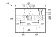
図1と図2は、ローカルインタコネクトを備えた半導体装置の実施例を表しており、図1は、平面図であり、図2は、図1に表されたライン2−2’に沿った断面図である。図1と図2を参照して、半導体装置200は、例えば、シリコン基板または他の半導体基板の基板100を含む。基板100は、当技術分野で周知のようにトランジスタ、レジスタと、他の半導体素子を含む各種の素子(図示されていない)を含むことができる。実施例では、基板は、互いに分離した少なくとも2つの活性領域100aと100bを有し、分離構造110、例えばシャロートレンチアイソレーション(STI)構造によって囲まれる。
1 and 2 show an embodiment of a semiconductor device having a local interconnect, FIG. 1 is a plan view, and FIG. 2 is taken along line 2-2 ′ shown in FIG. It is sectional drawing. Referring to FIGS. 1 and 2, a
誘電体層120は、基板上100に形成され、ILD層として用いられる。誘電体層120は、二酸化ケイ素、リンケイ酸ガラス(PSG)、ボロホスホシリケイトガラス(BPSG)、または例えばフッ化ケイ酸ガラス(FSG)または有機ケイ酸塩ガラス(OSG)などの低誘電率(k)材料であることができる。第1ゲート線構造116は、誘電体層120内と活性層100aの基板100上に配置される。第2ゲート線構造118は、誘電体層120内と活性層100bの基板100上に配置される。実施例では、第1ゲート線構造116と第2ゲート線構造118は、互いに分離され、同一線上に配列される。第1ゲート線構造116と第2ゲート線構造118のそれぞれは、対応する活性層の基板上のゲート誘電体層(絶縁膜)111を含むことができる。例えば、ポリシリコンのゲート電極113がゲート誘電体層111上に配置され、例えば窒化ケイ素層のキャップ層(図示されていない)によって覆われることができる。ゲートスペーサ115は、ゲート電極113の側壁に配置される。
The
第1対ソース/ドレイン領域101は、第1活性層100aの基板100上に形成され、第1ゲート線構造116の両側に設置される。第2対ソース/ドレイン領域103は、第2活性層100bの基板100上に形成され、第2ゲート線構造118の両側に設置される。結果、2つのトランジスタが第1と第2活性層100aと100b上にそれぞれ形成される。実施例では、第1対ソース/ドレイン領域101と第2対ソース/ドレイン領域103は、例えばN型、またはP型の同じ導電型、または異なる導電型を有することができる。例えば、第1対ソース/ドレイン領域101と第2対ソース/ドレイン領域103が同じ導電型を有する場合、第1ゲート線構造116と第2ゲート線構造118のゲート電極113は、図3に示されるように一体化して共通ゲート線構造を形成することができる。
The first pair of source /
一対の導電線112は、誘電体層(絶縁膜)120と第1ゲート線構造116と第2ゲート線構造118の両側の基板100上に位置される。よって一対の導電線112はゲート電極113と同じレベルにあり、各導電線112は、ローカルインタコネクトとして、第1ゲート線構造116と第2ゲート線構造118の同一側の第1対ソース/ドレイン領域101のうちの1つと第2対ソース/ドレイン領域103のうちの1つに電気的に接続する。実施例では、一対の導電線112はタングステン、銅、またはアルミニウムを含むことができる。また、各導電線112は、実質的に第1ゲート線構造116と第2ゲート線構造118に平行する。即ち導電線112と第1ゲート線構造116と第2ゲート線構造118は、同じ方向に沿って延伸される。
The pair of
誘電体層(絶縁膜)130は、誘電体層120と一対の導電線112の上方に形成され、IMD層として用いられる。誘電体層130は、単一層または多層構造であることができる。また、誘電体層130は、誘電体層120と同じまたは類似の材料を含むことができる。例えばタングステンまたは銅プラグの少なくとも1つの導電プラグ132は、それに接続されるように誘電体層130と一対の導電線112の1つの上に配置される。例えば銅層の金属層136は、誘電体層130と導電プラグ132の上方に配置され、その下方の導電線112によって2つのトランジスタに電気的接続される。
The dielectric layer (insulating film) 130 is formed above the
本発明に基づくと、第1と第2活性層100aと100b上に形成された2つのトランジスタが、従来の導電プラグに比べ、より大きな接触領域を提供する導電線112によって互いに電気的接続されることから、導電線112の接触抵抗は、従来の導電プラグより低い。即ち、半導体装置の装置密度は、従来の導電プラグを用いることと比較した時、ローカルインタコネクトとなる導電線112の低接触抵抗により、更に減少されることができる。また、2つのトランジスタのゲート電極線113が同一線上(即ちゲート電極113は、一直線に沿って延伸する)にあることから、ソース/ドレイン領域101と103の形成のプロセスは、比較的簡単である。また、同一線上のゲート電極113が一次元にだけ沿った単一導電層をパターニングすることで形成されることができるため、リソグラフィープロセスの間、よい線幅(CD)制御を得ることができる。また、ゲート電極113と導電線112が平行であることから、レイアウトも比較的簡単である。また、本発明に基づいたレイアウトは、比較的高密度のトランジスタレイアウトとなることができる。
In accordance with the present invention, two transistors formed on the first and second
以上、本発明の好適な実施例を例示したが、これは本発明を限定するものではなく、本発明の精神及び範囲を逸脱しない限りにおいては、当業者であれば行い得る少々の変更や修飾を付加することが可能である。従って、本発明が請求する保護範囲は、特許請求の範囲を基準とする。 The preferred embodiments of the present invention have been described above, but this does not limit the present invention, and a few changes and modifications that can be made by those skilled in the art without departing from the spirit and scope of the present invention. Can be added. Therefore, the protection scope claimed by the present invention is based on the claims.
100 基板
100a、100b 活性層
101 第1対ソース/ドレイン領域
103 第2対ソース/ドレイン領域
110 分離構造
111 ゲート誘電体層
112 導電線
113 ゲート電極
115 ゲートスペーサ
116 第1ゲート線構造
118 第2ゲート線構造
120、130 誘電体層
132 導電プラグ
136 金属層
200 半導体装置
100
Claims (10)
基板上に配置され、実質的に同一線上にある第1ゲート線構造と第2ゲート線構造、
前記第1ゲート線構造の両側の前記基板に形成された第1対ソース/ドレイン領域と前記第2ゲート線構造の両側の前記基板に形成された第2対ソース/ドレイン領域、及び
前記第1ゲート線構造と前記第2ゲート線構造の両側の前記基板上に配置され、それらが前記第1対ソース/ドレイン領域のうちの1つと前記第2対ソース/ドレイン領域のうちの1つに接続された一対の導電線を含む半導体装置。 A semiconductor device with a local interconnect,
A first gate line structure and a second gate line structure disposed on the substrate and substantially on the same line;
A first pair of source / drain regions formed on the substrate on both sides of the first gate line structure, a second pair of source / drain regions formed on the substrate on both sides of the second gate line structure, and the first A gate line structure and a second gate line structure are disposed on the substrate on opposite sides of the substrate and connected to one of the first pair of source / drain regions and one of the second pair of source / drain regions. A semiconductor device including a pair of conductive wires.
前記基板上に配置されたゲート誘電体層、
前記ゲート誘電体層上に配置されたゲート電極、及び
前記ゲート電極の側壁に配置されたゲートスペーサを含む請求項1に記載の半導体装置。 Each of the first gate line structure and the second gate line structure is:
A gate dielectric layer disposed on the substrate;
The semiconductor device according to claim 1, further comprising: a gate electrode disposed on the gate dielectric layer; and a gate spacer disposed on a sidewall of the gate electrode.
前記導電プラグに配置され、そこに接続される金属層を更に含む請求項1に記載の半導体装置。 The at least one conductive plug disposed on the pair of conductive lines and connected to one of the pair of conductive lines; and a metal layer disposed on the conductive plug and connected thereto. A semiconductor device according to 1.
Applications Claiming Priority (2)
| Application Number | Priority Date | Filing Date | Title |
|---|---|---|---|
| US12/212,034 US8138554B2 (en) | 2008-09-17 | 2008-09-17 | Semiconductor device with local interconnects |
| US12/212,034 | 2008-09-17 |
Publications (2)
| Publication Number | Publication Date |
|---|---|
| JP2010074158A true JP2010074158A (en) | 2010-04-02 |
| JP5388768B2 JP5388768B2 (en) | 2014-01-15 |
Family
ID=42006445
Family Applications (1)
| Application Number | Title | Priority Date | Filing Date |
|---|---|---|---|
| JP2009207011A Active JP5388768B2 (en) | 2008-09-17 | 2009-09-08 | Semiconductor device with local interconnect |
Country Status (5)
| Country | Link |
|---|---|
| US (1) | US8138554B2 (en) |
| JP (1) | JP5388768B2 (en) |
| KR (1) | KR101203936B1 (en) |
| CN (1) | CN101677102B (en) |
| TW (1) | TWI396254B (en) |
Cited By (4)
| Publication number | Priority date | Publication date | Assignee | Title |
|---|---|---|---|---|
| JP2014220501A (en) * | 2013-05-02 | 2014-11-20 | 台湾積體電路製造股▲ふん▼有限公司Taiwan Semiconductor Manufacturing Company,Ltd. | Standard cell metal structure directly above polysilicon structure |
| JP2016507909A (en) * | 2013-03-14 | 2016-03-10 | クアルコム,インコーポレイテッド | High density local interconnect structure |
| JP2017510069A (en) * | 2014-03-03 | 2017-04-06 | クアルコム,インコーポレイテッド | High performance standard cell |
| US10692808B2 (en) | 2017-09-18 | 2020-06-23 | Qualcomm Incorporated | High performance cell design in a technology with high density metal routing |
Families Citing this family (7)
| Publication number | Priority date | Publication date | Assignee | Title |
|---|---|---|---|---|
| DE102013110607B4 (en) * | 2013-05-02 | 2020-02-27 | Taiwan Semiconductor Manufacturing Company, Ltd. | Standard cell metal structure directly over polysilicon structure |
| US10177133B2 (en) | 2014-05-16 | 2019-01-08 | Taiwan Semiconductor Manufacturing Co., Ltd. | Semiconductor device including source/drain contact having height below gate stack |
| US9349859B1 (en) | 2015-01-29 | 2016-05-24 | Taiwan Semiconductor Manufacturing Company, Ltd. | Top metal pads as local interconnectors of vertical transistors |
| US10510688B2 (en) * | 2015-10-26 | 2019-12-17 | Taiwan Semiconductor Manufacturing Co., Ltd. | Via rail solution for high power electromigration |
| CN106653679A (en) * | 2015-11-03 | 2017-05-10 | 中芯国际集成电路制造(上海)有限公司 | Semiconductor device and forming method thereof |
| US10672708B2 (en) | 2015-11-30 | 2020-06-02 | Taiwan Semiconductor Manufacturing Co., Ltd. | Standard-cell layout structure with horn power and smart metal cut |
| DE102016114779A1 (en) * | 2016-05-19 | 2017-11-23 | Taiwan Semiconductor Manufacturing Company, Ltd. | Structure and method for a semiconductor device |
Citations (7)
| Publication number | Priority date | Publication date | Assignee | Title |
|---|---|---|---|---|
| JPH0395957A (en) * | 1989-09-08 | 1991-04-22 | Toshiba Corp | Semiconductor logic integrated circuit |
| JPH06204438A (en) * | 1992-12-28 | 1994-07-22 | Kawasaki Steel Corp | Semiconductor device |
| JPH07245396A (en) * | 1994-03-04 | 1995-09-19 | Sharp Corp | Semiconductor device and its manufacture |
| JP2000114262A (en) * | 1998-10-05 | 2000-04-21 | Toshiba Corp | Semiconductor device and its manufacture |
| JP2006157044A (en) * | 2001-01-30 | 2006-06-15 | Renesas Technology Corp | Production method for semiconductor integrated circuit device |
| JP2006202908A (en) * | 2005-01-19 | 2006-08-03 | Matsushita Electric Ind Co Ltd | Wiring structure of semiconductor device, manufacturing method thereof and circuit board |
| US20070181942A1 (en) * | 2006-01-16 | 2007-08-09 | Gerhard Knoblinger | Semiconductor circuit arrangement |
Family Cites Families (5)
| Publication number | Priority date | Publication date | Assignee | Title |
|---|---|---|---|---|
| JP2004111746A (en) | 2002-09-19 | 2004-04-08 | Fujitsu Ltd | Semiconductor device and manufacturing method therefor |
| US20050064629A1 (en) * | 2003-09-22 | 2005-03-24 | Chen-Hua Yu | Tungsten-copper interconnect and method for fabricating the same |
| US7701034B2 (en) * | 2005-01-21 | 2010-04-20 | Taiwan Semiconductor Manufacturing Company, Ltd. | Dummy patterns in integrated circuit fabrication |
| US7345344B2 (en) * | 2006-02-16 | 2008-03-18 | Freescale Semiconductor, Inc. | Embedded substrate interconnect for underside contact to source and drain regions |
| US7733698B2 (en) * | 2007-03-21 | 2010-06-08 | Qimonda Ag | Memory device, a non-volatile semiconductor memory device and a method of forming a memory device |
-
2008
- 2008-09-17 US US12/212,034 patent/US8138554B2/en active Active
-
2009
- 2009-09-08 JP JP2009207011A patent/JP5388768B2/en active Active
- 2009-09-16 CN CN2009101734177A patent/CN101677102B/en active Active
- 2009-09-16 KR KR1020090087579A patent/KR101203936B1/en active IP Right Grant
- 2009-09-17 TW TW098131332A patent/TWI396254B/en active
Patent Citations (7)
| Publication number | Priority date | Publication date | Assignee | Title |
|---|---|---|---|---|
| JPH0395957A (en) * | 1989-09-08 | 1991-04-22 | Toshiba Corp | Semiconductor logic integrated circuit |
| JPH06204438A (en) * | 1992-12-28 | 1994-07-22 | Kawasaki Steel Corp | Semiconductor device |
| JPH07245396A (en) * | 1994-03-04 | 1995-09-19 | Sharp Corp | Semiconductor device and its manufacture |
| JP2000114262A (en) * | 1998-10-05 | 2000-04-21 | Toshiba Corp | Semiconductor device and its manufacture |
| JP2006157044A (en) * | 2001-01-30 | 2006-06-15 | Renesas Technology Corp | Production method for semiconductor integrated circuit device |
| JP2006202908A (en) * | 2005-01-19 | 2006-08-03 | Matsushita Electric Ind Co Ltd | Wiring structure of semiconductor device, manufacturing method thereof and circuit board |
| US20070181942A1 (en) * | 2006-01-16 | 2007-08-09 | Gerhard Knoblinger | Semiconductor circuit arrangement |
Cited By (5)
| Publication number | Priority date | Publication date | Assignee | Title |
|---|---|---|---|---|
| JP2016507909A (en) * | 2013-03-14 | 2016-03-10 | クアルコム,インコーポレイテッド | High density local interconnect structure |
| JP2014220501A (en) * | 2013-05-02 | 2014-11-20 | 台湾積體電路製造股▲ふん▼有限公司Taiwan Semiconductor Manufacturing Company,Ltd. | Standard cell metal structure directly above polysilicon structure |
| US9158877B2 (en) | 2013-05-02 | 2015-10-13 | Taiwan Semiconductor Manufacturing Company, Ltd. | Standard cell metal structure directly over polysilicon structure |
| JP2017510069A (en) * | 2014-03-03 | 2017-04-06 | クアルコム,インコーポレイテッド | High performance standard cell |
| US10692808B2 (en) | 2017-09-18 | 2020-06-23 | Qualcomm Incorporated | High performance cell design in a technology with high density metal routing |
Also Published As
| Publication number | Publication date |
|---|---|
| TW201013842A (en) | 2010-04-01 |
| TWI396254B (en) | 2013-05-11 |
| US20100065921A1 (en) | 2010-03-18 |
| KR101203936B1 (en) | 2012-11-23 |
| CN101677102A (en) | 2010-03-24 |
| CN101677102B (en) | 2012-02-08 |
| KR20100032344A (en) | 2010-03-25 |
| JP5388768B2 (en) | 2014-01-15 |
| US8138554B2 (en) | 2012-03-20 |
Similar Documents
| Publication | Publication Date | Title |
|---|---|---|
| JP5388768B2 (en) | Semiconductor device with local interconnect | |
| KR100791339B1 (en) | An embeded semiconductor device including planarization resistant patterns and method for fabricating the same | |
| TW202115849A (en) | Semiconductor structure and method of fabricating the same | |
| KR20030047693A (en) | Semiconductor device | |
| JP3590034B2 (en) | Semiconductor capacitive element and manufacturing method thereof | |
| TWI755714B (en) | Sram device and manufacturing method thereof | |
| US6642604B2 (en) | Semiconductor device with resistor layer having heat radiation path to semiconductor substrate | |
| CN111463215B (en) | Memory structure and manufacturing method thereof | |
| US7768128B2 (en) | Semiconductor memory devices including a damascene wiring line | |
| TW201841331A (en) | Semiconductor device | |
| US20220359387A1 (en) | Structure and method of forming a semiconductor device with resistive elements | |
| TWI523172B (en) | Copper interconnect structure and methd for fabricating thereof | |
| KR100650192B1 (en) | Semiconductor device and method for forming the same | |
| US6776622B2 (en) | Conductive contact structure and process for producing the same | |
| TWI722546B (en) | Semiconductor device and method of fabricating the same | |
| JPWO2006061871A1 (en) | Semiconductor device | |
| KR102516407B1 (en) | Three-dimensional stacked semiconductor device and its manufacturing method | |
| JP2004104136A (en) | Method for manufacturing semiconductor integrated circuit device, and method for generating mask pattern | |
| TWI555122B (en) | Interconnection of semiconductor device and fabrication method thereof | |
| CN114944360A (en) | Semiconductor device and method for manufacturing the same | |
| JP2001068548A (en) | Semiconductor device and manufacture thereof | |
| KR0172725B1 (en) | Multi-layer metal wire forming method of semiconductor device | |
| KR20080055402A (en) | Wiring structure and method of forming the same | |
| KR20060083505A (en) | Method of forming a capacitor | |
| JP2005175252A (en) | Semiconductor device |
Legal Events
| Date | Code | Title | Description |
|---|---|---|---|
| A131 | Notification of reasons for refusal |
Free format text: JAPANESE INTERMEDIATE CODE: A131 Effective date: 20120522 |
|
| A977 | Report on retrieval |
Free format text: JAPANESE INTERMEDIATE CODE: A971007 Effective date: 20120524 |
|
| A601 | Written request for extension of time |
Free format text: JAPANESE INTERMEDIATE CODE: A601 Effective date: 20120820 |
|
| A602 | Written permission of extension of time |
Free format text: JAPANESE INTERMEDIATE CODE: A602 Effective date: 20120823 |
|
| A521 | Request for written amendment filed |
Free format text: JAPANESE INTERMEDIATE CODE: A523 Effective date: 20120924 |
|
| A131 | Notification of reasons for refusal |
Free format text: JAPANESE INTERMEDIATE CODE: A131 Effective date: 20130319 |
|
| A521 | Request for written amendment filed |
Free format text: JAPANESE INTERMEDIATE CODE: A523 Effective date: 20130617 |
|
| TRDD | Decision of grant or rejection written | ||
| A01 | Written decision to grant a patent or to grant a registration (utility model) |
Free format text: JAPANESE INTERMEDIATE CODE: A01 Effective date: 20130910 |
|
| A61 | First payment of annual fees (during grant procedure) |
Free format text: JAPANESE INTERMEDIATE CODE: A61 Effective date: 20131008 |
|
| R150 | Certificate of patent or registration of utility model |
Ref document number: 5388768 Country of ref document: JP Free format text: JAPANESE INTERMEDIATE CODE: R150 Free format text: JAPANESE INTERMEDIATE CODE: R150 |
|
| R250 | Receipt of annual fees |
Free format text: JAPANESE INTERMEDIATE CODE: R250 |
|
| R250 | Receipt of annual fees |
Free format text: JAPANESE INTERMEDIATE CODE: R250 |
|
| R250 | Receipt of annual fees |
Free format text: JAPANESE INTERMEDIATE CODE: R250 |
|
| R250 | Receipt of annual fees |
Free format text: JAPANESE INTERMEDIATE CODE: R250 |
|
| R250 | Receipt of annual fees |
Free format text: JAPANESE INTERMEDIATE CODE: R250 |
|
| R250 | Receipt of annual fees |
Free format text: JAPANESE INTERMEDIATE CODE: R250 |
|
| R250 | Receipt of annual fees |
Free format text: JAPANESE INTERMEDIATE CODE: R250 |
|
| R250 | Receipt of annual fees |
Free format text: JAPANESE INTERMEDIATE CODE: R250 |