JP2010073785A - 多層配線板およびその製造方法 - Google Patents
多層配線板およびその製造方法 Download PDFInfo
- Publication number
- JP2010073785A JP2010073785A JP2008237821A JP2008237821A JP2010073785A JP 2010073785 A JP2010073785 A JP 2010073785A JP 2008237821 A JP2008237821 A JP 2008237821A JP 2008237821 A JP2008237821 A JP 2008237821A JP 2010073785 A JP2010073785 A JP 2010073785A
- Authority
- JP
- Japan
- Prior art keywords
- sheet
- wiring board
- slurry
- multilayer wiring
- magnetic field
- Prior art date
- Legal status (The legal status is an assumption and is not a legal conclusion. Google has not performed a legal analysis and makes no representation as to the accuracy of the status listed.)
- Granted
Links
- 238000004519 manufacturing process Methods 0.000 title claims abstract description 57
- 239000002002 slurry Substances 0.000 claims abstract description 133
- 239000002184 metal Substances 0.000 claims abstract description 91
- 229910052751 metal Inorganic materials 0.000 claims abstract description 91
- 239000000843 powder Substances 0.000 claims abstract description 85
- 238000010030 laminating Methods 0.000 claims abstract description 36
- 238000003475 lamination Methods 0.000 claims abstract description 16
- 238000000034 method Methods 0.000 claims description 61
- 239000000758 substrate Substances 0.000 claims description 51
- 239000011230 binding agent Substances 0.000 claims description 17
- 239000003990 capacitor Substances 0.000 claims description 13
- 229920005989 resin Polymers 0.000 claims description 11
- 239000011347 resin Substances 0.000 claims description 11
- 230000000149 penetrating effect Effects 0.000 claims description 4
- 238000002156 mixing Methods 0.000 claims description 3
- 238000004804 winding Methods 0.000 claims description 2
- 230000001629 suppression Effects 0.000 abstract description 14
- 230000015572 biosynthetic process Effects 0.000 abstract description 3
- 230000008569 process Effects 0.000 description 31
- 230000000694 effects Effects 0.000 description 17
- 239000000956 alloy Substances 0.000 description 13
- 229910045601 alloy Inorganic materials 0.000 description 13
- 239000005300 metallic glass Substances 0.000 description 8
- 230000035699 permeability Effects 0.000 description 7
- 238000010586 diagram Methods 0.000 description 5
- 230000004907 flux Effects 0.000 description 5
- 238000003825 pressing Methods 0.000 description 5
- 238000001704 evaporation Methods 0.000 description 4
- 230000008020 evaporation Effects 0.000 description 4
- 239000011521 glass Substances 0.000 description 4
- 238000009413 insulation Methods 0.000 description 4
- 239000000203 mixture Substances 0.000 description 4
- KFZMGEQAYNKOFK-UHFFFAOYSA-N Isopropanol Chemical compound CC(C)O KFZMGEQAYNKOFK-UHFFFAOYSA-N 0.000 description 3
- YXFVVABEGXRONW-UHFFFAOYSA-N Toluene Chemical compound CC1=CC=CC=C1 YXFVVABEGXRONW-UHFFFAOYSA-N 0.000 description 3
- 230000008859 change Effects 0.000 description 3
- 239000010408 film Substances 0.000 description 3
- 230000009477 glass transition Effects 0.000 description 3
- 238000005096 rolling process Methods 0.000 description 3
- -1 for example Substances 0.000 description 2
- 239000000696 magnetic material Substances 0.000 description 2
- 238000010791 quenching Methods 0.000 description 2
- 230000000171 quenching effect Effects 0.000 description 2
- 229920005992 thermoplastic resin Polymers 0.000 description 2
- 229920001187 thermosetting polymer Polymers 0.000 description 2
- 239000010409 thin film Substances 0.000 description 2
- 229920002799 BoPET Polymers 0.000 description 1
- CTQNGGLPUBDAKN-UHFFFAOYSA-N O-Xylene Chemical compound CC1=CC=CC=C1C CTQNGGLPUBDAKN-UHFFFAOYSA-N 0.000 description 1
- 229910008423 Si—B Inorganic materials 0.000 description 1
- 230000009471 action Effects 0.000 description 1
- 238000013459 approach Methods 0.000 description 1
- 230000002238 attenuated effect Effects 0.000 description 1
- 230000005540 biological transmission Effects 0.000 description 1
- 238000006243 chemical reaction Methods 0.000 description 1
- 229910052804 chromium Inorganic materials 0.000 description 1
- 238000000576 coating method Methods 0.000 description 1
- 230000006835 compression Effects 0.000 description 1
- 238000007906 compression Methods 0.000 description 1
- 238000001816 cooling Methods 0.000 description 1
- 238000002425 crystallisation Methods 0.000 description 1
- 230000008025 crystallization Effects 0.000 description 1
- 230000002542 deteriorative effect Effects 0.000 description 1
- 239000002612 dispersion medium Substances 0.000 description 1
- 238000007606 doctor blade method Methods 0.000 description 1
- 230000005684 electric field Effects 0.000 description 1
- 230000005672 electromagnetic field Effects 0.000 description 1
- 238000005516 engineering process Methods 0.000 description 1
- 239000003822 epoxy resin Substances 0.000 description 1
- 230000001747 exhibiting effect Effects 0.000 description 1
- 238000009689 gas atomisation Methods 0.000 description 1
- 229910052737 gold Inorganic materials 0.000 description 1
- 229910052735 hafnium Inorganic materials 0.000 description 1
- LNEPOXFFQSENCJ-UHFFFAOYSA-N haloperidol Chemical compound C1CC(O)(C=2C=CC(Cl)=CC=2)CCN1CCCC(=O)C1=CC=C(F)C=C1 LNEPOXFFQSENCJ-UHFFFAOYSA-N 0.000 description 1
- 229920006015 heat resistant resin Polymers 0.000 description 1
- 238000010438 heat treatment Methods 0.000 description 1
- 238000007731 hot pressing Methods 0.000 description 1
- 229940089456 isopropyl stearate Drugs 0.000 description 1
- 239000007788 liquid Substances 0.000 description 1
- 239000000314 lubricant Substances 0.000 description 1
- 229910052750 molybdenum Inorganic materials 0.000 description 1
- 229910052758 niobium Inorganic materials 0.000 description 1
- QIQXTHQIDYTFRH-UHFFFAOYSA-N octadecanoic acid Chemical compound CCCCCCCCCCCCCCCCCC(O)=O QIQXTHQIDYTFRH-UHFFFAOYSA-N 0.000 description 1
- 229910052763 palladium Inorganic materials 0.000 description 1
- 229910052697 platinum Inorganic materials 0.000 description 1
- 229920000647 polyepoxide Polymers 0.000 description 1
- 239000004800 polyvinyl chloride Substances 0.000 description 1
- 229920000915 polyvinyl chloride Polymers 0.000 description 1
- 230000002040 relaxant effect Effects 0.000 description 1
- 229920002050 silicone resin Polymers 0.000 description 1
- 239000012798 spherical particle Substances 0.000 description 1
- 239000013526 supercooled liquid Substances 0.000 description 1
- 229910052715 tantalum Inorganic materials 0.000 description 1
- 229910052719 titanium Inorganic materials 0.000 description 1
- 229910052721 tungsten Inorganic materials 0.000 description 1
- 229910052720 vanadium Inorganic materials 0.000 description 1
- 238000009692 water atomization Methods 0.000 description 1
- 239000008096 xylene Substances 0.000 description 1
- 229910052726 zirconium Inorganic materials 0.000 description 1
Images


Landscapes
- Production Of Multi-Layered Print Wiring Board (AREA)
Abstract
【解決手段】本発明の多層配線板1は、軟磁性金属扁平粉末8の配向が局所的に異なる磁性シート4を2枚の配線板2、3の間に積層したものである。その製造方法は、スラリーシート形成工程、積層工程、局所磁場印加工程および硬化工程からなる。局所磁場印加工程においては、上下の配線板2、3の2枚の平板電極6、7に挟まれたスラリーシート4Sの軟磁性金属扁平粉末8に対して積層方向に磁場を局所印加し、所定の領域4A2の軟磁性金属扁平粉末8を縦方向に配向させる。
【選択図】図1
Description
2、3 配線板
4 磁性シート
4S スラリーシート(硬化前の磁性シート)
5 フレーム基板
6、7 平板電極
8 軟磁性金属扁平粉末
15 第1の空芯コイル
16 第2のコイル
16a、16b 2連コイル
Claims (15)
- コンデンサに用いられる1個または2個以上の平板電極を表面または裏面にそれぞれ有しており、各々の前記平板電極を対向させて積層されている2枚の配線板と、
軟磁性金属扁平粉末を混合した結着材を硬化させたシートであって前記2枚の配線板に挟まれている磁性シートと
を備えており、
前記2枚の配線板において積層方向に対向する2枚の平板電極に挟まれた前記磁性シートの軟磁性金属扁平粉末は、その法線方向が前記積層方向と直交するように配列されている
ことを特徴とする多層配線板。 - 前記2枚の配線板において積層方向に対向する2枚の平板電極に挟まれていない前記磁性シートの軟磁性金属扁平粉末は、その法線方向が前記積層方向と平行になるように配列されている
ことを特徴とする請求項1に記載の多層配線板。 - 前記磁性シートは、前記磁性シートの周縁を囲む枠形状または空洞形状であって硬化後における所望する前記磁性シートの厚さと同等の厚さまたは深さに設定されたフレーム基板の枠内または空洞内に挿入された状態において、前記2枚の配線板に挟まれている
ことを特徴とする請求項1または請求項2に記載の多層配線板。 - 前記フレーム基板は、樹脂製である
ことを特徴とする請求項3に記載の多層配線板。 - 各々の前記平板電極は、前記2枚の配線板における前記磁性シートとの接触面にそれぞれ形成されている
ことを特徴とする請求項1から請求項4のいずれか1項に記載の多層配線板。 - 前記2枚の配線板は、前記積層方向に貫通する1個または2個以上の硬化補助孔を有する配線板である
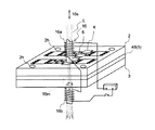
ことを特徴とする請求項1から請求項5のいずれか1項に記載の多層配線板。 - 軟磁性金属扁平粉末を結着材に混合して得たスラリーをシート状に加工することによりスラリーシートを形成するスラリーシート形成工程と、
表面または裏面にそれぞれ形成された1個または2個以上の平板電極を積層方向に対向させた2枚の配線板の間に前記スラリーシートを挟む積層工程と、
前記スラリーシート形成工程の後であって前記積層工程の前後いずれかにおいて、前記積層方向に対向する2枚の平板電極に挟まれる予定の又は挟まれた前記スラリーシートの軟磁性金属扁平粉末に対して前記スラリーシートの厚さ方向または前記積層方向に磁場を局所印加することにより、局所磁場印加された前記軟磁性金属扁平粉末をその法線方向が前記スラリーシートの厚さ方向または前記積層方向と直交するように配列させる局所磁場印加工程と、
前記積層工程および前記局所磁場印加工程の後において、前記2枚の配線板に挟まれた前記スラリーシートを積層状態において前記積層方向に熱加圧することにより、前記スラリーシートを硬化させた磁性シートを形成する硬化工程と
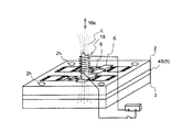
を備えることを特徴とする多層配線板の製造方法。 - 前記局所磁場印加工程においては、通電された第2のコイルの中心軸方向と前記スラリーシートの厚さ方向または前記積層方向とが平行になるように前記第2のコイルの端部周辺または内部に前記2枚の配線板に挟まれる予定の又は挟まれた前記スラリーシートを配置することにより、前記スラリーシートの厚さ方向または前記積層方向に磁場を印加する
ことを特徴とする請求項7に記載の多層配線板の製造方法。 - 前記第2のコイルは、同一軸上の2箇所において1本の金属線を同一方向に巻回することにより直列配置された2連コイルであり、
前記局所磁場印加工程においては、前記第2のコイルの内部であってその連結領域に前記2枚の配線板に挟まれる予定の又は挟まれた前記スラリーシートを配置する
ことを特徴とする請求項7に記載の多層配線板の製造方法。 - 前記スラリーシート形成工程の後であって前記局所磁場印加工程の前において、前記スラリーシートに混合されたすべての軟磁性金属扁平粉末に対して前記スラリーシートの厚さ方向または前記積層方向と直交方向に磁場を全体印加することにより、全体磁場印加された前記軟磁性金属扁平粉末をその法線方向が前記スラリーシートの厚さ方向または前記積層方向と平行になるように配列させる全体磁場印加工程を備える
ことを特徴とする請求項7から請求項9のいずれか1項に記載の多層配線板の製造方法。 - 前記全体磁場印加工程においては、通電された第1の空芯コイルの中心軸方向と前記スラリーシートの厚さ方向または前記積層方向とが直交するように前記第1の空芯コイルの内部に前記2枚の配線板に挟まれる予定の又は挟まれた前記スラリーシートを通過させることにより、前記スラリーシートの全域に対して前記スラリーシートの厚さ方向または前記積層方向と直交方向に磁場を印加する
ことを特徴とする請求項10に記載の多層配線板の製造方法。 - 前記スラリーシート形成工程の後であって前記積層工程の前において、枠形状または空洞形状であって前記磁性シートの厚さと同等の厚さまたは深さに設定されたフレーム基板の枠内または空洞内に前記スラリーシートを挿入するフレーム基板配置工程を備える
ことを特徴とする請求項7から請求項11のいずれか1項に記載の多層配線板の製造方法。 - 前記フレーム基板は、樹脂製である
ことを特徴とする請求項12に記載の多層配線板の製造方法。 - 各々の前記平板電極は、前記2枚の配線板における前記スラリーシートとの接触面にそれぞれ形成されている
ことを特徴とする請求項7から請求項13のいずれか1項に記載の多層配線板の製造方法。 - 前記2枚の配線板は、前記積層方向に貫通する1個または2個以上の硬化補助孔を有する配線板である
ことを特徴とする請求項7から請求項14のいずれか1項に記載の多層配線板の製造方法。
Priority Applications (1)
| Application Number | Priority Date | Filing Date | Title |
|---|---|---|---|
| JP2008237821A JP4980322B2 (ja) | 2008-09-17 | 2008-09-17 | 多層配線板およびその製造方法 |
Applications Claiming Priority (1)
| Application Number | Priority Date | Filing Date | Title |
|---|---|---|---|
| JP2008237821A JP4980322B2 (ja) | 2008-09-17 | 2008-09-17 | 多層配線板およびその製造方法 |
Publications (2)
| Publication Number | Publication Date |
|---|---|
| JP2010073785A true JP2010073785A (ja) | 2010-04-02 |
| JP4980322B2 JP4980322B2 (ja) | 2012-07-18 |
Family
ID=42205325
Family Applications (1)
| Application Number | Title | Priority Date | Filing Date |
|---|---|---|---|
| JP2008237821A Expired - Fee Related JP4980322B2 (ja) | 2008-09-17 | 2008-09-17 | 多層配線板およびその製造方法 |
Country Status (1)
| Country | Link |
|---|---|
| JP (1) | JP4980322B2 (ja) |
Cited By (2)
| Publication number | Priority date | Publication date | Assignee | Title |
|---|---|---|---|---|
| JP2012019036A (ja) * | 2010-07-07 | 2012-01-26 | Nec Corp | 電子部品の実装構造及び実装方法 |
| CN114208399A (zh) * | 2020-07-16 | 2022-03-18 | 友晏爱科技有限公司 | 减少电磁波吸收率的系统 |
Citations (8)
| Publication number | Priority date | Publication date | Assignee | Title |
|---|---|---|---|---|
| JPH03280497A (ja) * | 1990-03-29 | 1991-12-11 | Toshiba Ave Corp | 電子回路基板 |
| JPH1079593A (ja) * | 1996-09-05 | 1998-03-24 | Tokin Corp | 磁性プリプレグとその製造方法及びそれを用いたプリント配線基板 |
| JP2001308227A (ja) * | 2000-04-21 | 2001-11-02 | Mitsui Chemicals Inc | 電子回路基板用複合材料 |
| JP2003229694A (ja) * | 2002-02-05 | 2003-08-15 | Sony Corp | 電磁波吸収体およびその製造方法 |
| JP2005109174A (ja) * | 2003-09-30 | 2005-04-21 | Hitachi Cable Ltd | 電波吸収体及びその製造方法 |
| JP2005228908A (ja) * | 2004-02-13 | 2005-08-25 | Mitsubishi Materials Corp | 高周波磁芯材及びその製造方法並びに該磁芯材を備えたアンテナ |
| JP2008028165A (ja) * | 2006-07-21 | 2008-02-07 | Shin Etsu Polymer Co Ltd | ノイズ抑制構造体および多層プリント回路基板 |
| JP2010050254A (ja) * | 2008-08-21 | 2010-03-04 | Alps Electric Co Ltd | 磁性シートの製造方法、磁性シートおよび磁性シートの製造装置 |
-
2008
- 2008-09-17 JP JP2008237821A patent/JP4980322B2/ja not_active Expired - Fee Related
Patent Citations (8)
| Publication number | Priority date | Publication date | Assignee | Title |
|---|---|---|---|---|
| JPH03280497A (ja) * | 1990-03-29 | 1991-12-11 | Toshiba Ave Corp | 電子回路基板 |
| JPH1079593A (ja) * | 1996-09-05 | 1998-03-24 | Tokin Corp | 磁性プリプレグとその製造方法及びそれを用いたプリント配線基板 |
| JP2001308227A (ja) * | 2000-04-21 | 2001-11-02 | Mitsui Chemicals Inc | 電子回路基板用複合材料 |
| JP2003229694A (ja) * | 2002-02-05 | 2003-08-15 | Sony Corp | 電磁波吸収体およびその製造方法 |
| JP2005109174A (ja) * | 2003-09-30 | 2005-04-21 | Hitachi Cable Ltd | 電波吸収体及びその製造方法 |
| JP2005228908A (ja) * | 2004-02-13 | 2005-08-25 | Mitsubishi Materials Corp | 高周波磁芯材及びその製造方法並びに該磁芯材を備えたアンテナ |
| JP2008028165A (ja) * | 2006-07-21 | 2008-02-07 | Shin Etsu Polymer Co Ltd | ノイズ抑制構造体および多層プリント回路基板 |
| JP2010050254A (ja) * | 2008-08-21 | 2010-03-04 | Alps Electric Co Ltd | 磁性シートの製造方法、磁性シートおよび磁性シートの製造装置 |
Cited By (2)
| Publication number | Priority date | Publication date | Assignee | Title |
|---|---|---|---|---|
| JP2012019036A (ja) * | 2010-07-07 | 2012-01-26 | Nec Corp | 電子部品の実装構造及び実装方法 |
| CN114208399A (zh) * | 2020-07-16 | 2022-03-18 | 友晏爱科技有限公司 | 减少电磁波吸收率的系统 |
Also Published As
| Publication number | Publication date |
|---|---|
| JP4980322B2 (ja) | 2012-07-18 |
Similar Documents
| Publication | Publication Date | Title |
|---|---|---|
| US10943725B2 (en) | Sheet-shaped inductor, inductor within laminated substrate, and method for manufacturing said inductors | |
| KR101983136B1 (ko) | 파워 인덕터 및 그 제조방법 | |
| US9589716B2 (en) | Laminated magnetic component and manufacture with soft magnetic powder polymer composite sheets | |
| KR101686989B1 (ko) | 파워 인덕터 | |
| US8329087B2 (en) | Method of manufacturing magnetic sheet | |
| CN110828108B (zh) | 含金属磁性粒子的磁性基体和含该磁性基体的电子部件 | |
| JP7485505B2 (ja) | インダクタ | |
| KR101662206B1 (ko) | 파워 인덕터 | |
| CN103971892A (zh) | 磁芯、电感器和包括电感器的模块 | |
| JP2006286934A (ja) | コモンモードチョークコイル | |
| CN101040354B (zh) | 层叠型陶瓷电子部件的制造方法及复合层叠体 | |
| JP6456729B2 (ja) | インダクタ素子およびその製造方法 | |
| KR20140148110A (ko) | 금속 자성체 분말 및 그 형성 방법, 그리고 상기 금속 자성체 분말을 이용하여 제조된 인덕터 | |
| WO2022209565A1 (ja) | 積層体及びその製造方法 | |
| JP4843820B2 (ja) | 電波吸収多層基板 | |
| JP4980322B2 (ja) | 多層配線板およびその製造方法 | |
| JP2008072073A (ja) | コイル部品 | |
| JP2006060432A (ja) | 電波送受信アンテナ | |
| JP5177641B2 (ja) | 積層体、及びアンテナ | |
| JP6291789B2 (ja) | 積層コイル部品 | |
| US20190198237A1 (en) | Coil electronic component | |
| JP4851640B2 (ja) | 加速器用アモルファスコア及びそれを用いた加速器 | |
| Zhou et al. | Superior soft magnetic properties and mechanical strength in nanocomposites employing a double-percolating microstructure | |
| JP2001332411A (ja) | 複合磁性材料 | |
| CN222190443U (zh) | 电感器和电子设备 |
Legal Events
| Date | Code | Title | Description |
|---|---|---|---|
| A621 | Written request for application examination |
Free format text: JAPANESE INTERMEDIATE CODE: A621 Effective date: 20101119 |
|
| TRDD | Decision of grant or rejection written | ||
| A977 | Report on retrieval |
Free format text: JAPANESE INTERMEDIATE CODE: A971007 Effective date: 20120322 |
|
| A01 | Written decision to grant a patent or to grant a registration (utility model) |
Free format text: JAPANESE INTERMEDIATE CODE: A01 Effective date: 20120327 |
|
| A01 | Written decision to grant a patent or to grant a registration (utility model) |
Free format text: JAPANESE INTERMEDIATE CODE: A01 |
|
| A61 | First payment of annual fees (during grant procedure) |
Free format text: JAPANESE INTERMEDIATE CODE: A61 Effective date: 20120418 |
|
| FPAY | Renewal fee payment (event date is renewal date of database) |
Free format text: PAYMENT UNTIL: 20150427 Year of fee payment: 3 |
|
| R150 | Certificate of patent or registration of utility model |
Ref document number: 4980322 Country of ref document: JP Free format text: JAPANESE INTERMEDIATE CODE: R150 Free format text: JAPANESE INTERMEDIATE CODE: R150 |
|
| S533 | Written request for registration of change of name |
Free format text: JAPANESE INTERMEDIATE CODE: R313533 |
|
| R350 | Written notification of registration of transfer |
Free format text: JAPANESE INTERMEDIATE CODE: R350 |
|
| LAPS | Cancellation because of no payment of annual fees |